JP4215394B2 - Hierarchical caching method of configuration data in a data flow processor and a component having a programmable cell structure of two or more dimensions - Google Patents
Hierarchical caching method of configuration data in a data flow processor and a component having a programmable cell structure of two or more dimensions Download PDFInfo
- Publication number
- JP4215394B2 JP4215394B2 JP2000533829A JP2000533829A JP4215394B2 JP 4215394 B2 JP4215394 B2 JP 4215394B2 JP 2000533829 A JP2000533829 A JP 2000533829A JP 2000533829 A JP2000533829 A JP 2000533829A JP 4215394 B2 JP4215394 B2 JP 4215394B2
- Authority
- JP
- Japan
- Prior art keywords
- instruction
- instruction sequence
- configuration
- data
- trigger
- Prior art date
- Legal status (The legal status is an assumption and is not a legal conclusion. Google has not performed a legal analysis and makes no representation as to the accuracy of the status listed.)
- Expired - Fee Related
Links
Images


Classifications
-
- G—PHYSICS
- G06—COMPUTING; CALCULATING OR COUNTING
- G06F—ELECTRIC DIGITAL DATA PROCESSING
- G06F15/00—Digital computers in general; Data processing equipment in general
- G06F15/76—Architectures of general purpose stored program computers
- G06F15/78—Architectures of general purpose stored program computers comprising a single central processing unit
- G06F15/7867—Architectures of general purpose stored program computers comprising a single central processing unit with reconfigurable architecture
-
- G—PHYSICS
- G06—COMPUTING; CALCULATING OR COUNTING
- G06F—ELECTRIC DIGITAL DATA PROCESSING
- G06F12/00—Accessing, addressing or allocating within memory systems or architectures
- G06F12/02—Addressing or allocation; Relocation
- G06F12/08—Addressing or allocation; Relocation in hierarchically structured memory systems, e.g. virtual memory systems
- G06F12/0802—Addressing of a memory level in which the access to the desired data or data block requires associative addressing means, e.g. caches
- G06F12/0806—Multiuser, multiprocessor or multiprocessing cache systems
- G06F12/0811—Multiuser, multiprocessor or multiprocessing cache systems with multilevel cache hierarchies
-
- G—PHYSICS
- G06—COMPUTING; CALCULATING OR COUNTING
- G06F—ELECTRIC DIGITAL DATA PROCESSING
- G06F12/00—Accessing, addressing or allocating within memory systems or architectures
- G06F12/02—Addressing or allocation; Relocation
- G06F12/08—Addressing or allocation; Relocation in hierarchically structured memory systems, e.g. virtual memory systems
- G06F12/0802—Addressing of a memory level in which the access to the desired data or data block requires associative addressing means, e.g. caches
- G06F12/0806—Multiuser, multiprocessor or multiprocessing cache systems
- G06F12/0813—Multiuser, multiprocessor or multiprocessing cache systems with a network or matrix configuration
-
- G—PHYSICS
- G06—COMPUTING; CALCULATING OR COUNTING
- G06F—ELECTRIC DIGITAL DATA PROCESSING
- G06F12/00—Accessing, addressing or allocating within memory systems or architectures
- G06F12/02—Addressing or allocation; Relocation
- G06F12/08—Addressing or allocation; Relocation in hierarchically structured memory systems, e.g. virtual memory systems
- G06F12/0802—Addressing of a memory level in which the access to the desired data or data block requires associative addressing means, e.g. caches
- G06F12/0806—Multiuser, multiprocessor or multiprocessing cache systems
- G06F12/084—Multiuser, multiprocessor or multiprocessing cache systems with a shared cache
Abstract
Description
【0001】
発明の背景
従来の技術
この出願が基礎とする従来技術は、特許出願 196 54 846.2-53 (2次元またはそれ以上の次元のプログラミング可能なセルマトリックス(FPGA,DPGA等)を備えたデータフロープロセッサ(DFP)およびコンポーネントの自立的ダイナミックリロード方法)、ならびに特許出願 196 54 593.5-53 (ランタイムにプログラミング可能なコンポーネントの再コンフィグレーション方法)に記載されている。そこにはDFPならびにFPGA、DPGAおよび従来技術による類似のコンポーネントをコンフィグレーションおよび再コンフィグレーションする方法について記述されており、それによれば別個に形成され中央で上位に位置するマイクロコントローラに似たコンポーネントが、下位に位置するかなりパッシブな制御ユニットの配分の役割を担っている。
【0002】
問題点
1つまたは複数のコンポーネントの各部分(たとえばセル(CEL))の再コンフィグレーションを制御する中央のグローバルなユニットを使用すると、数多くの様々な再コンフィグレーション要求を一度に処理しなければならないときに隘路となってしまう。既述のコンポーネントの並列性の長所は、上記のような中央ユニットによって制約されてしまう。なぜならばそれらは典型的な「ボトルネック」を成しており、データ処理がこれにより著しく緩慢になってしまう。さらに、ロードすべきコンフィグレーションへのイベントソースの割り当てが問題となる。それというのも、コンフィグレーションメモリの絶対アドレスで動作が行われるからである。したがって再コンフィグレーションユニットには一種のメモリ管理システムが含まれていなければならず、これはオペレーティングシステムの場合のように、どのメモリ領域がどのコンフィグレーションによって使われるのかをいっしょに記録する。さらに付加的な問題として、リソース(たとえばCEL)の管理が挙げられる。この場合、各CEL(セル)が正確に1度だけしか、リコンフィグレーション要求により始められたアルゴリズムしかも残りの周辺のCELも使用するアルゴリズムへ与えられないようにしておかなければならない。さもないとデッドロックの生じる可能性がある。
【0003】
再コンフィグレーションの問題点をもう一度はっきりとさせるため、以下の実例を挙げる。複数のCELから成る1つのマトリックスはコンフィグレーションされておらず、RESET状態にある。各CELは、それらが再コンフィグレーションされた状態にあるか否かを表すことができる。マトリックスにおけるすべてのCELはコンフィグレーションに対しスタンバイ状態にあり、つまり再コンフィグレーション可能な状態にある。第1のコンフィグレーションルーチン(KR1)がロードされ、その際、マトリックスは完全には使用されない。コンフィグレーションされたCELは、それがコンフィグレーション可能な状態にあるという合図を消す。まだコンフィグレーションされていないCELのグループに、第1のコンフィグレーションルーチンとは独立した第2のコンフィグレーションルーチン(KR2)がロードされる。この場合、第3のコンフィグレーションルーチンはロードできない。なぜならばこれらのセルは第1および/または第2のコンフィグレーションルーチンに必要とされ、それらは使われるためコンフィグレーション可能な状態にはないからである。必要とされるCELが開放されるまで、すなわちKR1とKR2が終了してしまうまで、KR3は停止されなければならない。KR1およびKR2の実行中、第4のコンフィグレーションルーチン(KR4)および第5のコンフィグレーションルーチン(KR5)に対するロード要求がさらに生じるけれども、それらをすべてただちに実行することはできない。なぜならばそれらは、KR1およびKR2により使われるCELを利用するからである。KR3とKR4は部分的に同じCELを使用するが、KR5はKR3およびKR4によるCELのいずれも使用しない。
【0004】
KR3からKR5を順序どおりにリドードするための要求は以下の通りである:
1.KR3からKR5を、ロード要求に従い時間的な順序ができるかぎり保持されるようロードすること。
【0005】
2.最大限の並列性を維持するため、互いに依存せずつまり共通のCELをもたないできるかぎり数多くのKRをロードすること。
【0006】
3.各KRが互いにブロックし合ってはならない。つまりKR3は部分的にロードされるが、他のCELが部分的にロードされたKR4にブロックされているので、それ以上はロードできない。他方、KR4もそれ以上はロードできない。それというのも、同様に必要とされるCELがKR3によりブロックされているからである。このことにより典型的なデッドロック状態が引き起こされる。
【0007】
4.KRを生成したコンパイラにとって、時間的に重なるKRの実行を識別し、コンフリクト状態を解消するのは不可能である。
【0008】
この場合、実現すべき回路にかかるコストと最適な結果との間の関係を、できるかぎり良好なものにしなければならない。つまり本発明の目的は、できるかぎりわずかなコストでフレキシブル、パラレルかつデッドロックのないコンフィグレーションを行うことができるようにし、時間的にも計算上も僅かな手間しかかけずにそれを実行できるようにすることである。この場合、以下の基本的な問題を解決しなければならない:
−K3だけしかロードしないのであれば、そのやり方によってもデッドロックは発生しないが、KR5もロード可能であろうことから、それは最適ではない。
【0009】
−KR3をロードし、KR4をロードしなければ、KR5はKR4を、それが後続のロードプロセスにあたり最高優先度をもつようあらかじめ記録しておかねばならず、このことは管理の手間が著しくかかることを意味する。
【0010】
デッドロックのない状態は、以下で述べる方法によって得られる:
本発明による改善、課題
本発明の基本的な課題は、階層構造をもち各レベルに何度も現れることのできるユニット(以下ではコンフィグレーションテーブルCTと称する)を構成することであり、その際にCTの個数を、最上位レベルにおいてちょうど1つのCTが存在するよう、最下位の階層段から最上位の階層段に向かって低減させる。各CTは他のパラレルなCTとは無関係に、コンフィグレーション可能な複数のエレメント(CEL)のコンフィグレーションおよびコントロールを行う。高い方の階層段におけるCTは、低い階層におかれたCTのためのコンフィグレーションルーチンを一時記憶することができる。低い階層におかれた複数のCTが同一のコンフィグレーションルーチンを必要とする場合、そのルーチンが高い階層におかれたCTにおいて一時記憶され、個々のCTから呼び出される。この場合、高い階層におかれたCTは該当するコンフィグレーションルーチンをグローバルな共通のコンフィグレーションメモリから1度呼び出すだけであり、これによってキャッシュ効果が達成される。コンフィグレーション可能なコンポーネントから離れて、マイクロプロセッサ、DFPあるいは複数の計算機構をもつ同等のものにおいて、命令キャッシュおよびデータキャッシュ用のキャッシュ方法として本発明を使用することができる。この場合、用途に応じて、以下で説明するユニットのうちのいくつか(たとえばFILMO)を省略できるが、階層構造については基本的に変更されない。したがってこの使用法はサブセットとみなされ、これについてはこれ以上詳しくは立ち入らない。ここで述べる方法が慣用のキャッシュ方法よりも著しく有利な点は、データおよび/またはコードが選択的に、つまり精密にアルゴリズムに合わせてチューニングされた方法に基づきキャッシュされることである。さらに本発明によれば、完全にデッドロックのない大きいセル構造の再コンフィグレーションを行えるようにもなる。
【0011】
本発明の説明
従来のように中央のグローバルなユニットを、すべてのコンフィグレーション要求を処理する1つのコンポーネントに統合する代わりに、本発明によればその役割を担うことができ階層構造(ツリー構造)で配置された複数のアクティブなユニットが設けられている。その際、最下位レベル(階層構造におけるリーフ)からの要求は、その要求を処理できなかったときだけ、1つ上の階層レベルへ転送される。これらのステップは最上位レベルに到達するまで、存在するすべてのレベルに対して繰り返される。最上位のレベルはさらに上位に位置する内部または外部のコンフィグレーションメモリとつながっており、これにはこのプログラム実行にいつか必要とされるコンフィグレーションデータが含まれている。
【0012】
コンフィグレーションユニットにおけるツリー構造によって、コンフィグレーションデータに対する一種のキャッシングが達成される。コンフィグレーションに対するアクセスは、主としてローカルで行われる。最も不利な状況として、該当するデータが階層構造で配置されたCTのいずれにも存在しない場合、上位に位置するコンフィグレーションメモリからコンフィグレーションをロードする必要がある。その際、ロードすべきコンフィグレーションについて固定的な時間順序を取り入れ、コンフィグレーションを1つのリストにまとめることによって、デッドロックが回避される。CELのステータス情報はロード前に保護され、これによりコンフィグレーションのリスト全体が使われている間、変更されずに保持される。
【0013】
CTの基礎
コンフィグレーションテーブル(CT)は、同期信号いわゆるトリガに対して応答するアクティブなユニットである。このトリガは、慣用の算術ユニットまたは論理ユニット、アドレス発生器、演算ユニット等のための複数の電子コンポーネント(以下ではコンフィグレーション可能なエレメントCELと称する)から成る2次元またはそれ以上の次元のマトリックスにより生成される。発生するトリガに基づき、CT内で所定のアクションが引き起こされる。この場合、CTの役割は、複数のCELの制御を引き継ぎ、それらの算術演算および/または論理演算を求めることである。殊に、CELをコンフィグレーションおよび再コンフィグレーションする必要がある。この役割をCTが担うが、これはそれぞれ複数の個々のコンフィグレーションワード(KW)から成る可能な複数のコンフィグレーションルーチン(KR)を管理し、複数のCELをトリガ条件に基づきKRのうちの1つまたは複数によってコンフィグレーションすることによって行われる。その際、CELには、それぞれコンフィグレーションワードの1つまたは複数が含まれており、これにはコンフィグレーションすべきCELのアドレスが設けられている。この場合、KRは完全かつ適正に複数のCELにコピーされなければならず、ここで複数のCELを、それぞれ異なるが完全に実行されるKRによりコンフィグレーションされるグループにまとめておくことができる。その際、すべてのCELはグループ内で次のように結線されている。すなわち、必要とされる再コンフィグレーションの確認後、グループ分けされたすべてのCELに対し共通の信号(ReConfig)により、各CELがデータ処理を終了し再コンフィグレーション可能な状態へ移行しなければならないことが通知されるよう、グループ内で結線されている。
【0014】
デッドロックのない再コンフィグレーションの基礎
ランタイムに再コンフィグレーション可能なシステムにおいて生じる問題点は、そのつど2つの部分が互いに待機し、したがってデッドロック状況の生じた状態にシステムが陥ってしまう可能性のあることである。
【0015】
このような問題点は、新しいコンフィグレーションをシステムに必ずまるごとロードするかまったくロードしないかだけにし、あるいは一種のタイムアウト手法を適用すれば回避できよう。とはいえこれにより一連の欠点(所要スペース、伝播時間等)や問題点が生じてしまう。たとえば、
−コンフィグレーションをロードできない場合の措置
−コンフィグレーションをロードする順序の管理
−場合によってはCELにロードすることができるかもしれない他のコンフィグレーションが留意されないため、パフォーマンスの落ち込み
などである。
【0016】
以下で説明する方法によれば、これらの問題点を除去することができる。これは従来技術によるDFPシステムから出発するものである。
【0017】
あるCELからトリガ信号がCTへ送られる。このCTはトリガのソースを突き止め、ルックアップテーブルによりロードすべきコンフィグレーション(KR)を選択する。到来するトリガ信号は阻止され、目下のコンフィグレーションが完全に処理されてしまうまで、他のいかなるトリガも受けつけない。1つのコンフィグレーションは複数の命令から成り、これは複数のCELの集合へ伝送される。しかし伝播時間にコンフィグレーション可能なシステムでは、いかなるコンフィグレーション命令(KW)も実行できるという保証がない。これはたとえば、アドレッシングされたコンフィグレーション可能なエレメント(CEL)がそのタスクを依然として終了せず、したがって新たなコンフィグレーションデータを受け取ることができないようなことになって失敗してしまうおそれがある。パフォーマンスの劣化を避ける目的で、(対応するCELが再コンフィグレーション可能な状態になくコンフィグレーションを拒否(REJECT)したため)実行できなかったすべてのコンフィグレーション命令が、FIFOに従い(以下で詳しく説明する)専用メモリ(FILMO)内に最後に存在するコンフィグレーション命令の後ろに書き込まれる。その後、次のコンフィグレーション命令が同じやり方で処理される。これは1つのコンフィグレーションの最後に到達するまで繰り返される。
【0018】
ついでCTは再び、場合によっては別のコンフィグレーションをロードできるようにするためトリガ信号を受けつける状態へ移行する。この状態でCTはFILMOをタイマ制御により規則的なインターバルで処理する。
【0019】
ロードすべきコンフィグレーションの優先順位づけは、本来ロードすべきコンフィグレーションが処理される前にCTがメモリFILMOを通過することにより行われる。FIFOに似たFILMOの構造により、先行のトリガ要求中に完全には処理できなかったKWが新たに処理すべきWKよりも高い優先順位を自動的にもつようにされる。メモリ(FILMO)の処理にあたり、コンフィグレーション命令によりアドレッシングされるコンフィグレーション可能な各エレメント(CEL)は、KWの送信前または送信中、状態「コンフィグレーション可能」にあるか否かについてテストされる。この状態「コンフィグレーション可能」(ACCEPT)にあれば、データが伝送され、メモリFILMOから消去される。状態「コンフィグレーション不可能」(REJECT)にあれば、データはFILMO内に残され、次のスキャン時に新たに処理される。CTはFILMO内の次のエントリを処理する。これはFILMOの最後に到達するまで繰り返される。その後、トリガ信号の発生によりアクティブにされた本来のコンフィグレーションが処理される。この場合、FILMOの構造はFIFO方式に対応し、つまり最も古いエントリが一番最初に処理される。新たなKRがロードされなくてもFILMOを処理する目的で、FILMOはタイマ制御により規則的なインターバルでスキャンされる。
【0020】
関与していないそれ以外のコンフィグレーション可能なエレメント(CEL)はこのフェーズ中、パラレルに処理され続け、それらの機能に作用が及ぼされない。これによりCTがFILMOを処理している間、1つまたは複数のコンフィグレーション可能なエレメント(CEL)が状態「コンフィグレーション可能」へ移行するような状況が起こり得る。CTはFILMO内における任意の個所で処理状態になる可能性があるため、以下のような状況の発生する可能性がある:
CTは、アドレッシングされたコンフィグレーションすべきエレメント(CEL)が状態「コンフィグレーション可能」におかれていないような最初の命令の処理するよう試みる。これによりCTは次の命令(KW)を続行する。同じ時点で、1つまたは複数のコンフィグレーション可能なエレメントが状態「コンフィグレーション可能」に移行し、それには第1のコンフィグレーション命令により書き込まれたかもしれないコンフィグレーション可能なエレメントも含まれる。CTは第2のコンフィグレーション命令(KW)を処理し、これは第1のコンフィグレーション命令と同じであるが他のコンフィグレーションからのものであるコンフィグレーション可能なエレメント(CEL)を使用する。この時点で、コンフィグレーション可能なエレメント(CEL)は状態「コンフィグレーション可能」にあり、命令をうまく処理することができる。
【0021】
これにより、最初にロードすべきコンフィグレーションが実際にやはり最初に仕上げられる、という保証がもはやなくなる。この場合、部分的に完成した2つのコンフィグレーションの存在する可能性があり、それらは完全にロードできるようにするためにそれぞれ他方のコンフィグレーションのコンフィグレーション可能なエレメントを必要とする。ここでデッドロック状態が発生し、これは図18に示されている。この場合、コンフィグレーションAとコンフィグレーションBをコンフィグレーションしようとしている。CTは、コンフィグレーションAとコンフィグレーションBにおけるハッチングされた部分をすでにロードしている。コンフィグレーションAは完成のために、コンフィグレーションBのうち明るく二重にハッチングされた領域をさらに必要とし、コンフィグレーションBは完成のために、コンフィグレーションAのうち暗く二重にハッチングされた領域を必要とする。これら両方のコンフィグレーションはともにまだ完全には終わっておらず、したがって機能を果たす能力もないので、双方のコンフィグレーションのいずれについてもこれら2つのコンフィグレーションの一方が取り除かれるであろう終了状態には入らない。これらのコンフィグレーションは両方とも、まだ必要としているコンフィグレーション可能なエレメントが開放されるのを待っている。
【0022】
本発明による方法の場合、デッドロックは次のようにして回避される。すなわち、CTがFILMOの処理前にコンフィグレーション可能なすべてのエレメントの状態を捕捉し、それに従って事象が終了するまでいかなる変化ももはや許可せず、つまり発生する変化を無視するようにしている。換言すれば、コンフィグレーション可能なすべてのエレメントの状態がFILMOの処理前に保護され、あるいはFILMOの処理中、状態の変化が阻止される。1つの実現可能な技術的形態は、コンフィグレーション可能な各エレメントにおいて1つのレジスタを使用し、そのレジスタへFILMO処理前の状態を入れて保護することである。CTは捕捉された状態だけに基づき動作し、コンフィグレーション可能なエレメントの目下の状態によっては動作しない。これにより、処理すべき命令(KW)がコンフィグレーション可能なエレメント(CEL)の等しい状態を確実に見出せるようになる。このステップは、1つまたは複数のコンフィグレーション可能なエレメントがFILMOの処理中に状態「コンフィグレーション可能」へ移行することを排除していない。この変化はCTには処理中にすぐさまは見えず、次の実行開始になってようやく気がつくことになる。
【0023】
コンフィグレーションの順序
所定のアルゴリズムのコンフィグレーションのためにどうしても必要であるのは、KWをCELに書き込む順序を正確に守ることである。たとえば有用であるのは、CELをバスシステムへつなぐ前、まずはじめにバスシステムのコンフィグレーションを行うことであり、それによってCELが他のルーチンによって使われているバスと接続されることがなくなる。換言すれば、対応するバスコネクションのコンフィグレーションを事前に行うことができたときにだけ、CELのコンフィグレーションが行われる。
【0024】
本発明による方法の場合、固定的な順序の遵守は以下のようにして達成される:
後続のKWのコンフィグレーションにとって重要な構成をもつコンフィグレーションワード(KW)は、特別に表される(以下ではKWRと称する)。このようなKWRのコンフィグレーションが失敗すると、該当するコンフィグレーションルーチン(KR)内における後続のすべてのKWがFILMOに書き込まれ、この過程では実行されない。FILMOのスキャン時にも、順序がKWRの後方にありコンフィグレーションの失敗したすべてのKWは、目下の過程では実行されない。
【0025】
キャッシュ方法
CT構造は階層構造であって、つまり1つのコンポーネント内に複数のCTレベルが存在する。この配置構成は、有利には木構造(CTツリー)に対応する。この場合、ルートCT(Root−CT)は外部のコンフィグレーションメモリ(ECR)であり、これにはすべてのKRが対応づけられて格納されている一方、リーフにはコンフィグレーション可能なエレメント(CEL)が対応づけられており、これによって個々のKRが呼び出される。中間レベルのCTにはそれぞれコンフィグレーション可能なエレメントが対応づけられており、これらは同じ階層段階におかれている。各CTにはローカルな内部メモリが対応づけられている。このメモリは、新たに格納すべきKRのためにもはやスペースがないとき、あるいはそのことが特別なCT命令(REMOVE)によって明示的に要求されたとき、部分的に消去される。この場合、消去は、せいぜいのところもはや要求されないKRだけが、あるいはREMOVE命令によって明示的に表されたKRだけが消去されるよう、消去判定基準に従いKRごとに行われる。同様にKRは、新たにロードすべきKRをメモリに書き込むのにちょうど必要な数だけ、つまりそれにちょうど必要な個数のメモリが空きになるよう、1つ1つ消去される。これにより、キャッシュ効果の最適化のためできるかぎり多くのKRをメモリ内に残しておくことができる。
【0026】
このことの利点は、任意のCTxの下に配置された各CTつまりCTツリー内でずっと上に存在するCTは、CTx内には格納されていないKRを、外部のコンフィグレーションメモリECRから要求するのではなく、CTxからダイレクトに受け取ることである。これにより、複数のレベルにわたってキャッシュ構造が生じる。CTツリーにおけるデータ伝送の煩雑性殊にECRにおける所要メモリ帯域幅が著しく低減される。
【0027】
換言すれば各CTは、下に位置するCTのKRをバッファリングする。つまり、下の方に位置するCTは必要とするKRを上に位置するCTからダイレクトに受け取るのであって、外部のECRに対するメモリアクセスは不要である。必要とするKRが高い方に位置するCTのいずれにも存在していないときにだけ、ECRへのアクセスを介してKRをロードすればよい。これにより、KRのための格別効率的な階層キャッシュ構造が得られる。この構造に基づき実現可能な消去判定基準も得られるが、これは用途に応じて経験的に決められることになる。いくつかの可能性を挙げておく:
−最も古いエントリーの消去
−最も小さいエントリーの消去
−最も大きいエントリーの消去
−最も稀にしか呼び出されないエントリーの消去
CT階層構造の基礎
キャッシュ効果を達成するため、CTはツリー構造における1つの階層にまとめられる。個々のノード(CT)の間にバスシステム(Inter−CT−Bus)が存在し、これはそれぞれ上方のノード(CT)を複数の下位のノード(CT)と接続する。その際、下位のノード(CT)は上位のノード(CT)に対しデータを要求し、それに応じて上位のノードは下位のノードへデータを送る。下位のノードはステータス情報を互いに交換し、そのためにいっそう上位のノード間のネットワークが利用され、それらのネットワークはそれに応じてアドレスを分解する必要がある。
【0028】
CT階層構造およびアドレッシング
CT階層構造は、個々のCTのアドレッシングのためにバイナリツリーを利用できるように配置されている。つまり、最下位のアドレスビットはツリーの個々のリーフを表し、他の各アドレスビットはそれぞれ1つの階層レベルだけ上を選択するのである。したがって各CTは一義的なアドレスを有している。
【0029】
下記の表には、個々のアドレスビットが個々のレベルにどのように割り当てられているかが示されている。
【0030】
【表1】

* = 使用されるアドレスビット
- = 使用されないアドレスビット
複数のCTから成るグループに上位のCTを割り当てる場合、そのグループにおける複数のアドレスビットがそれに応じてまとめられる。
【0032】
次の表には、個々のアドレスビットが個々のレベルにどのように割り当てられているのかが示されており、その際、レベル0には8個のCTをもつグループが存在している(アドレスビット 2..0)
【0033】
【表2】
* = 使用されるアドレスビット
- = 使用されないアドレスビット
バイナリツリーの構造は1次元または多次元で行うことができ、これは各次元ごとに1つのバイナリツリーを形成することによって行われる。
【0035】
特定のCT(TARGET)がアドレッシングされ、これは開始させるCT(INITIATOT)が正確なターゲットアドレスを指示するか、あるいはTAGETが相対的にアドレッシングされる。
【0036】
次に、相対アドレスの評価について詳しく説明する:
2次元のアドレッシングのための相対アドレスフィールドの実例:
【0037】
【表3】
ビット15は、次に高い階層段のCTを選択すべきときにセットされる。また、ビット14はブロードキャストを表し、したがってすべてのCTを選択する。X/Yアドレスは、INITIATORのアドレスを出発点としたTARGETのアドレスを表している。
【0039】
アドレスは符号付きの "signed" 整数である。アドレスフィールドのY/Xアドレスを目下のアドレスポジションに加えることで、TARGETが求められる。各レベルは特定のアドレス幅(Addresswidth)をもっている。加算器はこの幅に対応している。
【0040】
加算においてオーバーフローやアンダーフローが生じたということは、アドレッシングされたCTが目下のノードよりも下には位置しておらず、アドレス要求がその上に位置するCT(次に高いノード)へ転送されることを意味する。オーバーフローやアンダーフローが発生しなければ、TARGETは目下のノードよりも下に位置している。目下のレベルで計算されたアドレスビット(表を参照)により、目下のノードのすぐ下に位置するCTが選択される。そこからそれぞれ相応に計算されたアドレスビットに基づき、次に低いCT(ノード)が選択される。
【0041】
CH階層構造におけるアクセスの優先順位づけ
内部CTバスへのアクセスはアービタによって管理される。この場合、下位のすべてのノードに対し等しい優先順位が与えられる。上位のノードはそれよりも高い優先順位をもっている。これにより、上位のノードから下位へ向かって伝送されるアクセス、あるいはINITIATORからすでにかなり進んだアクセスが、他のアクセスよりも優先される。
【0042】
CTの基本構造
CTについての以下の概要から、個々のコンポーネントに関する概観を得ることにする。以下では、各コンポーネントについて詳細に説明する。
【0043】
CTのコアはコントロールステートマシン(CTS)であって、これはコンフィグレーションルーチン(KR)のすべての処理を制御する。各CTにはガーベージコレクタ(GC)が配分されており、これはCTのメモリ(CTR)からのKRの除去を制御する。なお、FILMOはまだ処理すべきKWの管理を担い、LOADステートマシンはKRのロードを制御する。
【0044】
メモリ(CTR)は慣用の書き込み読み出しメモリとして構成されていて、その際、技術的に可能なすべてのインプリメンテーションを適用することができ、個々のCTおよびその下位におかれたCTに対するKRのローカルな記憶のために用いられる。特別な事例として、ASICやPLD(従来技術参照)に似た機能をコンポーネントに設ける目的で、メモリ(CTR)をROM、EPROM、EEPROM、フラッシュROM等として構成することができる。
【0045】
CTRアドレスを生成するため、ロード可能なカウンタとして構成された多数のポインタが使用される:
1.フリーポインタ(FP)。これはCTR内における最後のKRの後ろにある最初の空きメモリロケーションを指す。
【0046】
2.ガーベージポインタ(GP)。これはガーベージコレクタ(GC)によりCTRから除去すべきエントリを指す。
【0047】
3.ムーブポインタ(MP)。これが指すCTR内のメモリロケーションとは、除去すべきでない最終的なコンフィグレーションワード(KW)つまりKRのエントリが、その位置からGPによって規定されたエントリーへコピー/移動されるようなロケーションである。
【0048】
4.プログラムポイン(PP)。これは目下CTSにより実行されているKWを指す。
【0049】
KWは、出力インタフェース(OUT)を介して属するCELへ転送される。CELは、それがコンフィグレーション可能な状態にあるかぎり、KWの受領確認をする(ACCEPT)。KWが拒否された場合(REJECT)、あとになってプログラムポインタを利用することなく再度、アドレッシングされたCELへ書き込むため、FIFOに類似したメモリ(FILMO)内にそれが一時的にバッファリングされる。
【0050】
CTSは、KRを処理するための要求をトリガ信号により受け取る。このトリガ信号は、望ましくないトリガをフィルタリング除去(マスキング除去)するフィルタであるマスクを通過する。従来技術に従って、マスクをANDゲート(AND)におり構成することができ、このゲートによればトリガとイネーブル信号とがAND結合される。トリガは、優先順位の付けられたラウンドロビン・アービタ(Round-Robin-Arbiter, SCRR-ARB)を介してバイナリ信号に変換される。優先順位の付けられたラウンドロビン・アービタにより、ラウンドロビン・アービタの平等性の利点と、1つのクロック内における次のイネーブルの検出つまり優先順位アービタの利点とが合わせられる。
【0051】
マスキングされたトリガは、アドレスとして第1のルックアップテーブル(LUT1)へ供給され、このルックアップテーブルは、アドレスとして到来するトリガに対し該当するKRのIDを割り当てて、データラインへ送出する。第2のルックアップテーブル(LUT2)において、KRのIDがCTR内におけるKRのメモリロケーションのアドレスに割り当てられる。第2のルックアップテーブルはトリガ信号の割り当てに利用されるだけでなく、IDをパラメータとして用いる使われる命令のアドレス割り当てのためにも利用される。トリガ信号と該当するIDとの対応づけは、あとで説明する命令”REFERENCE”によりLUT1にエントリされる。LUT2の管理つまりIDとCTRにおけるアドレスとの対応づけは、CTSとGCにより自動的に行われる。
【0052】
CTの理解を深めるため、実現可能な基本命令セットについて以下に示す:
1.BEGIN<ID>
BEGIN<ID>により、コンフィグレーションルーチンの開始が表される。<ID>は、コンフィグレーションルーチンにおける一義的な識別番号を表す。
【0053】
2.STOP
STOPにより、コンフィグレーションルーチンの最後が表される。この位置において、コンフィグレーションテーブル(CT)はコンフィグレーションルーチンの処理を終了する。ガーベージコレクタ(GC)は、そのコンフィグレーションルーチンにおけるエントリの除去を終了する。
【0054】
3.EXECUTE<ID>
コンフィグレーションルーチンの最初(BEGIN<ID>)にジャンプする。このルーチンがCTのメモリ内に存在していなければ、その上に位置するCTに対しそれが要求され、ないしはメモリからロードされる。
【0055】
4.LOAD<ID>
KR<ID>をその上に位置するCTに対して要求する。
【0056】
5.REMOVE<ID>
GCを呼び出す。その目的は、コンフィグレーションルーチン<ID>をBEGIN<ID>からSTOPまでCTのメモリから除去し、除去されたコンフィグレーションルーチンによってもメモリの隙間が生じないようになるまで、後続のコンフィグレーションルーチンを前へ押し出すことである。
【0057】
6.PUSH<FORCED><ADDRESS><DATA><EXIT>
コンフィグレーションデータ<DATA>をレジスタ<ADDRESS>へ書き込む。<FORCED>がセットされていると、該当するターゲットレジスタのRECONFIGフラグがセットされていなくても、データが書き込まれる。<EXIT>は、REJECTのときに後続のKWRが引き続き実行されるのを中止するKWRであるこを表すために用いられる。
【0058】
7.MASK<SR><TRIGGER>
<SR>(Set/Reset)に依存して、トリガマスクを<TRIGGER>によりセットするか、あるいはそれを<TRIGGER>によりリセットする。
【0059】
8.WAIT<UNMASKED><TRIGGER>
コンフィグレーションルーチンの処理を停止し、トリガ<TRIGGER>を待つ。<UNMASKED>がセットされていれば、待っているトリガに対しトリガマスクの状態とは無関係に応答する。
【0060】
9.トリガ<TRIGGER><CT#>
トリガのバイナリ値を、CT#によりアドレッシングされた上位のCTへ送る。
【0061】
10.GETBUS/GETCTS
内部CTバスへのコネクションを確立する。
【0062】
11.LOOSEBUS/LOOSECTS
内部CTバスへのコネクションを解除する。
【0063】
12.REFERENCE<TRIGGER><ID>
アドレス<TRIGGER>においてLUT1へ値<ID>を書き込み、これによりトリガ信号に対し特定のKRが割り当てられる。
【0064】
命令 EXECUTE,LOAD,REMOVE,PUSH,MASK,WAIT,TRIGGER,REFERENCEは、BEGINと...STOPで括られた中でのみ有効である。この括りの外では命令は実行されない。
【0065】
コンフィグレーションルーチン(KR)の構造は以下のようになる:
BEGIN<ID>;
...
有効な命令
...
STOP;
間接アドレッシング(参照)
CTのキャッシュ原理によりCT内におけるKRのバッファリングが可能となり、ここでKRは下位に位置する異なる複数のCTまたはCELによって利用される。下位のユニットからコンポーネント(たとえばRAM、周辺装置)の外部インタフェースへのアクセスが行われる場合、外部インタフェースの種々のアドレスまたは一部分を記憶する必要がある。これにより基本的には、必要とされる個々のKRの内容が区別されることになろう。キャッシングはもはや不可能である。この場合、間接参照により対策が講じられる。この目的で専用のKR(以下ではIKRと称する)が用いられ、これは必要な外部パラメータをもっており、それをセットする。必要に応じトリガを介して、異なる階層レベルにおける他の異なるKRが呼び出される。IKRの最後から本来のKRが呼び出される。IKRだけはキャッシングできないが他方、呼び出されたKRはまったく一義的であり、そのためキャッシュ可能である。ここで有用であるのは、IKRのサイズを絶対的な最小値まで低減することであり、つまりもっぱら外部の異なるパラメータと本来のKRの呼び出しだけにすることである。
【0066】
間接的なコンフィグレーションルーチン(IKR)は以下のように構成されている:
BEGIN<ID>;
...
xxx; 有効な命令、この場合、外部の周辺装置だけを制御する
TRIGGER<ID>; 周辺プロセスに対するスタート、ストップまたはロード要求
...
GOTO<ID>; 本来のKRへのジャンプ
STOP;
特別な事例:
1.WAIT_FOR_BOOT
この命令は、CTRの最初のアドレスだけに有効である。ブートプロセス中、まずはじめに完全なブートKRがCTRに書き込まれるが、Boot−KR BEGIN<0>の開始シーケンスではない。その個所(アドレス1)にはWAIT_FOR_BOOTがあり、これはRESET時に自動的にセットされる。Boot−KR全体がCTRに書き込まれてからはじめて、WAIT_FOR_BOOTがBEGIN<0>によって上書きされ、CTSがBoot−KRの処理を始める。WAIT_FOR_BOOTはプログラム内に現れてはならない。
【0067】
2.BOOT<CT−ID>
BOOT<CT−ID>は、どのCTに後続のBoot−KRを書き込むべきであるかを表す。BOOT<CT−ID>後にはBEGINは続かず、Boot−KRはSTOPによってではなく、あとにくるBOOT<CT−ID>によって終了する。そしてSTOPによってブートプロセスが終了する。BOOT<CT−ID>はプログラム内に現れてはならない。
【0068】
ブートプロセス
RESET後、最上位の階層レベル(ROOT−CT)のCTはBoot−KRを下位の階層のCTにロードする。この目的で、ROOT−CTに対応づけられた外部のコンフィグレーションメモリ(ECR)内の定められたアドレス(BOOT−ADR)へのジャンプが存在する。ROOT−CTはこのジャンプを実行し、ブートシーケンスに到達する。これは以下のように構成されている:
BOOT<CT−ID0>; COMMAND; COMMAND; ...
BOOT<CT−ID1>; COMMAND; COMMAND; ...
...
BOOT<CT−IDn>; COMMAND; COMMAND; ...
STOP;
ブートプロセス中、まずはじめにBoot−KR全体が、<CT−ID>により表されたCTのアドレス2からCTR内に書き込まれる。Boot−KR(BEGIN<0>)の開始シーケンスは、アドレス1には書き込まれない。その個所にはWAIT_FOR_BOOTがあり、これはRESET時に自動的にセットされる。Boot−KR全体がCTRに書き込まれ、ROOT−CTが次のBOOT<CT−ID>に到達してはじめて、STOPがBoot−KRの終わりでCTRに書き込まれ、WAIT_FOR_BOOTがBEGIN<0>によって上書きされる。CTSはBoot−KRの処理を始める。
【0069】
コンフィグレーションルーチンのロード
Boot−KR外でコンフィグレーションルーチンを要求するために、3つの基本メカニズムが存在する。
【0070】
1.CTSによるLOAD<ID>の実行
2.CTSによるEXECUTE<ID>の実行、ここで該当するIDをもつKRはCTR内には存在していない。
【0071】
3.トリガの発生、これはLUT1を介して<ID>に変換され、それに属するKRはCTR内には存在していない。
【0072】
すべて3つの事例における進行は同じである:
要求されるKRのIDはLUT2へアドレスとして供給される。LUT2は、CTR内に有効なアドレスが存在するか否かについてチェックする。これが存在しなければ、つまりLUT2において<ID>が値0を指していれば、LOAD<ID>がCTSへ送られる。
【0073】
それに応じてCTSが、階層的に上位にあるCTにおいて<ID>に該当するKRを要求する。この要求はトリガ形式で上位のCTに到達し、それによって相応に評価される。上位のCTは要求されたKRを要求されたCTへ送信する。データは、FREE−POINTER(FP)の指すアドレスからCTRへ書き込まれ、その際、FPは書き込みアクセスごとに1だけ高められる。FPがCTRの上限に到達すると、ガーベージコレクタ(GC)が呼び出され、CTR内で最下位のKRが除去されてCTRが圧縮されるようになる。そのときFPが新たにセットされる。この過程は、ロードすべきKRが完全にCTRに納まるまで行われる。
【0074】
コンフィグレーションメモリにおけるジャンプテーブル
ROOT−CTに割り当てられたコンフィグレーションメモリには、アプリケーションのためにロードしなければならないKR全体が含まれている。外部のコンフィグレーションメモリ(ECR)には、定められたアドレス(ARD−BOOT)のところにブートコンフィグレーションルーチンへのジャンプがおかれている。任意であるがアプリケーション内部で固定的に定められた長さをもつ別の所定のメモリ領域(LUT−ECR)には、個々のKRへのジャンプがおかれている。この場合、個々のKRの<ID>はECR内のアドレスとして用いられ、そこには個々のKRの開始アドレスが存在する。これによりKRが間接的にアドレッシングされるのである:
ID −> LUT−ECT −> KR
コンフィグレーションメモリ内におけるKRの変更
ID<A>をもつKRは変更されることになる。まずはじめにHOSTはID<A>のための新たなKRを、ECR内の空きメモリロケーションへ書き込む。ID<A>は、上位のユニット(HOST)におけるコンフィグレーションメモリ内のKRの新たなアドレスといっしょに、そのために設けられたROOT−CTのレジスタに書き込まれる。ROOT−CTは、その下に位置するすべてのCTへ命令REMOVE<A>を送信する。それに応じてすべてのCTは、STOPに到達したときまたはIDLEサイクルの間すなわちKRが実行されなければただちに、そのIDに関連するKRをCTRから除去し、LUT2はアドレス<A>に”NoAdr”をセットする。つまりこのことは、LUT2内にID<A>に対する有効なアドレスエントリが存在しないことを意味する。ID<A>が再度要求されれば、欠けているエントリ(”NoAdr”)は強制的にLUT2への<A>ではなく、各CTはECRに対しKR<A>を新たに要求する。
【0075】
FILMO
KRは主として命令PUSHから成り、これは新たなコンフィグレーションワードを所定のアドレスに書き込む。アドレッシングされたコンフィグレーション可能なエレメント(CEL)が新たなコンフィグレーションを受け入れる準備が整っていないため(REJECT)、タイプKWのコンフィグレーションワードの書き込みが不可能であれば、コンフィグレーションワードはアドレッシングされたコンフィグレーション可能なエレメント(CEL)ではなく、以下ではFILMOと称するメモリへ書き込まれる。後続の命令は、再度コンフィグレーションワードを書き込むことができなくなるまで通常どおり処理され、できなくなればそのワードはFILMOへ書き込まれる。
【0076】
アドレッシングされたコンフィグレーション可能なエレメント(CEL)が新たなコンフィグレーションを受け入れる準備が整っていないため(REJECT)、タイプKWRのコンフィグレーションワードの書き込みが不可能であれば、コンフィグレーションワードはアドレッシングされたコンフィグレーション可能なエレメント(CEL)の代わりに、以下ではFILMOと称するメモリへ書き込まれる。KRが終了するまでの後続のすべての命令は、CELではなくFILMOへダイレクトに書き込まれる。
【0077】
FILMOは、IDLEサイクル中であって新たなKRがそのつど実行される前にスキャンされる。この場合、最も古いデータワードのところで始まり、従来技術によるFIFOに従い、読み出されたFIFOの各ワードがアドレッシングされたエレメントへ送られる。ここでアドレッシングされたエレメントはすでに、コンフィグレーションワードを受け取る準備ができていなければならない。データワードを最初から書き込むことができるかぎり(つまりアドレッシングされたコンフィグレーション可能なエレメント(CEL)がスタンバイ状態にあれば)、FIFOの形式でFILMOからエントリが除去される。コンフィグレーションワードを書き込むことができなければ、それはとばされてFILMOからは除去されない。FIFOとは異なり、とびこされたコンフィグレーション後のデータがさらに読み出される。とびこされたコンフィグレーションワードの後に書き込むことのできるコンフィグレーションワードは、FILMOの実装に従って以下のとおりとなる。すなわち、
1.書き込み済とマーキングされ、FILMOからは消去されない。ここで書き込み済とマーキングされたコンフィグレーションワードは、後続のスキャンにおいてはもはや読み出されず、あるいはとばされたコンフィグレーションワードがもはやその前に存在しなければ、ただちに消去される。
【0078】
あるいは、
2.FILMOから消去される。この場合、コンフィグレーションワードは消去されたコンフィグレーションワードの前と後ではそのまま得られ、ここで消去のため後続のワードが前方(上方)へ、あるいは先行のワードが後方(下方)へシフトされ、その際、コンフィグレーションワードの順序は強制的に維持される。
【0079】
新たなKRが実行されると、アドレッシングされたエレメント(CEL)へCTSにより書き込むことのできなかったコンフィグレーションワード(KW)が、新たにFILMOに付加され、つまりKWはFILMOの(読み出し方向で)最後に書き込まれる。FILMOがいっぱいになると、すなわちコンフィグレーション値のための空きエントリが存在しないと、KRの実行が停止される。FILMOは、十分にコンフィグレーションワードを書き込むことができ、それに応じて多数の空きエントリが発生するまでスキャンされ、その後、KRが引き続き処理される。FILMOはFIFOに似たメモリを成しており、これは常に最も古いエントリから直線的にスキャンされる。しかしFIFOとは異なり、エントリがとばされる(First In Linear Multiple Out)。
【0080】
コンフィグレーションテーブル−ステートマシン(CTS)の機能
コンフィグレーションテーブル・ステートマシン(CTS)はCTの制御の役割を担う。これはKRの命令を実行し、到来するトリガに対し応答する。そしてこれはFILMOの管理の役割を担い、殊にアイドルサイクル中、KRの実行前にそれを読み出す。これはLUT構造により生成された信号illegal<TRG>(Illegalトリガ、図1の0102参照)とload<ID>に対して応答する。load<ID>は、LUT2においてキャッシュミスが生じたとき(0105)、あるいはIDにより参照されるKR/IKRが消去済とマーキングされていたとき(0107)に生成される。これは上位のCTの制御信号に対して応答する。図2〜図7には、命令処理のためのインプリメンテーションの実例が描かれている。
【0081】
上位のCTへの制御信号
−illegal<TRG>(0102)
上位のCTは、未知のトリガ<TRG>が発生していることを指示する。
【0082】
−load<ID>(0105/0107)
上位のCTに対し<ID>のロードを要求
−trigger<TRG><CT#>(0108)
トリガ<TRG>を上位のCTまたはアドレッシングされたCT<CT#>に送信
上位のCTの制御信号
−remove<ID>(図15,1513参照)
CTに対し<ID>の消去を要求
−write_to_FP<data>(図2,0205参照)
データをCTへ送信。データは占有されているメモリの最後に付加される。
【0083】
ガーベージコレクタ(GC)の機能
CTRには2つの問題点がある:
1.LOAD命令またはEXECUTE命令またはトリガが、CTR内に存在していないKRのIDを指している場合、KRをリロードしなければならない。しかし状況によっては、要求されたKRをロードするのに十分なスペースがCTR内にない。
【0084】
2.REMOVE<ID>が発生したとき、対応するKRをCTRから除去しなければならない。この場合、KRがCTRの最後にはなければ、隙間が生じてしまう。新たなKRをロードしても、この隙間は場合によっては完全には埋められず、あるいはこの隙間が新たなKRに対し小さすぎるかもしれない。その結果、CTRのフラグメンテーションが発生する。ガーベージコレクタの役割は、KRをCTRを除去し、新たなエントリのためのスペースを確保することであり、かつエントリ除去後のCTRを、残ったすべてのKRが閉じたブロックとして相前後してメモリ内に位置するようにし、しかも空いたメモリブロックが閉じたブロックとしてCTRの最後に位置させることである。このことにより最適に、しかもメモリロケーションの損失なく新たなKRをロードすることができる。
【0085】
トリガパルスの評価
各CTは、それらの個々の階層平面に属する複数のトリガ信号に対するコンタクトを有しており、これらのトリガ信号は1つのバスへ送られてまとめられる。到来するトリガはマスクを介して評価され、つまりイネーブルにされたトリガ信号が転送される。イネーブルにされたトリガ信号は、クロック同期してサンプルレジスタ内にバッファリングされる(サンプリングされる)。アービタは格納されているトリガ信号のうちの1つを選択し、信号をバイナリベクトルへ変換する。選択されたトリガ信号はサンプルレジスタから消去される。そしてバイナリベクトルは第1のルックアップテーブル(LUT1)へ転送され、このテーブルによってバイナリベクトルが呼び出すべきコンフィグレーションルーチン(KR)の識別番号(ID)へ変換される。IDは、第2のルックアップテーブル(LUT2)においてCTメモリ(CTR)内のKRのアドレスに変換される。CTステートマシン(CTS)はそのプログラムポインタ(PP)を上記のアドレスにセットし、KRの実行を開始する。ここで前提とするのは、マスクを介してイネーブルにされた各トリガがLUT1内に対応するエントリをもっていることである。これが欠けていると、エラー状態がCTSへ伝送され(Illegaltrigger)、その際、各ID=”NoAdr”は存在しないエントリとして評価される。”NoAdr”は、インプリメンテーションに依存して選定されるトークンである。LUT2内にエントリがなければ、つまりIDに該当するKRがCTR内に存在しなければ、ロード要求がCTSへ送られる(load<ID>)。
【0086】
上位のCTへのトリガパルスの送信
KRをロードするための上位のCTへの既述のインタフェースのほかに、任意に定義できる命令とはいえ殊にトリガベクトルを交換するための別のインタフェースも存在する。その際にCTは、
−他のすべてのCTへ命令を送るか(BROADCAST)
−またはアドレッシングされた任意のCTへ命令を送る(ADDRESSED)
命令”Triggervektor”はバイナリ値を表しており、これは受け取ったCTにおけるLUT2内のエントリを参照している。トリガベクトルの送信はたとえば、IKR内でKRをさらに別のCTにおいてスタートさせ、これによりたとえば周辺装置やメモリを制御するために必要される。
【0087】
上位のCTへトリガベクトルを転送するために2つのメカニズムが存在する。
【0088】
1.LUT1に1つのビットを付け加え、このビットによって、メモリの内容がKR IDとみなされるのか、あるいはトリガパルスのバイナリ値とみなされるのかを表すようにする。トリガパルスが生じているのであれば、LUT1のデータ内容がそのままトリガとして上位のCTへ送られる。
【0089】
2.命令TRIGGERによってトリガのバイナリ値を表すことができ、それがそのまま上位のCTへ送られる(代案としてトリガ値の代わりにそのままIDを伝送してもよい)。
【0090】
トリガベクトルを介して未知のCTにおいてKRをスタートさせるためには、デッドロック状況を生じさせないよう同期方式を作る必要がある。この方式によって、複数のCTから成る特定のグループ内のKRだけしかこのグループ内の他のCTにおいて別のKRをスタートさせないよう、注意を払わなければならない。複数のKRを同時にスタートさせると、CEL平面における既述のデッドロックと同じように、各CT間でデッドロックの生じてしまう可能性がある。
【0091】
このような方式の基本原理は以下のようにして進行する:
KRは以下のように構成されている:
...
GETCTS/GETBUS
TRIGGER<ID>,<CT#>
TRIGGER<ID>,<CT#>
...
LOOSECTS/LOOSEBUS
...
CT(INITIATOR)におけるKR内の命令”GETCTS”によって、後続の信号で他のCT(TAGET)が送られることを表す。トリガ<ID>,<CT#>によって、スタートさせるべきKRのIDが一義的なID CT#をもつCTへ送られる。この場合、トリガの送信はまず最初にすぐ上位のCTに対して行われ、これはCT#に応じてトリガをそのCT空間内の今度は下位のCTへ送るか、またはそれにとって上位のCTへ送る(CT階層を参照)。命令が到達すれば、それが受領確認を行う。
【0092】
CTにより命令が実行されると、命令の優先順位識別子がそのつど1つだけ高められる。命令の転送要求がCT内における別の要求にぶつかれば、最も低い優先順位をもつ命令が取り下げられる。
【0093】
このことにより以下のことが保証される。
【0094】
a)オーバラップしたシステム内においてある時点で1つの命令だけしか伝播されず、このためただ1つのKRだけしかスタートせず、このことで必要とされるデッドロックのない状況が得られるようになる。
【0095】
b)それまでで最も遠くへは伝播されなかった命令が取り下げられ、このことでパフォーマンスを高めることができる。命令の取り下げ後、GETCTS/LOOSECTS内の先行するすべての命令も同様に取り下げられ、つまりINITIATORがすべてのTARGETへ信号DISMISSを送り、GETCTSの待機時間後にKRの実行が開始される。命令区間GETCTS...LOOSECTS内におけるすべてのトリガの受領確認がINITIATORへ送られる。受領確認が到来するたびに次の命令の処理が続けられる。命令LOOSECTSに到達すると、INITIATORはすべてのTARGETへ信号GOを送る。これによりTARGET−CTが、トリガにより伝送されたIDをもつKRの実行をスタートさせる。TARGETはトリガの発生後に状態を変化させ、その状態においてTARGETはGOまたはDISMISSの発生を待つ。
【0096】
インプリメンテーションが改善されたことで、さらに容易に変更される手法が得られる:
1つの階層平面における1つのグループ内の各CT間にバスシステムが存在する(Inter−CT−Bus)。このバスシステムは、グループにおけるすべてのCTとそのグループのすぐ上に位置するCTとをつないでいる。機能的にGETCTSに似た命令GETBUSにより、バスシステムがCTにより調停される。この命令は、バスシステムを介して同じグループのCTへ転送される。アドレッシングされたCT#がグループ内に存在していなければ、上位に位置するCTによって自動的にその上位に位置するバスが調停され、命令が転送される。調停されたバスはINITIATORに対応づけられたままになり、したがって拒否されるまで、または命令LOOSEBUSがバスに発せられるまで、他のすべてのCTに対しは阻止される。LOOSEBUSはLOOSECTSと対比できる。命令LOOSEBUSの実行前、GO信号が関与するすべてのCTへ送られる。これは命令LOOSEBUSまたは前につなげられた特別な命令によって行われる。命令殊にトリガは、やはり既述の基本的手法に従って処理される。バスシステムを調停できなかったとき、拒否が生じる。調停の際、1つの平面におけるCTがそれぞれ等しく優先順位づけされ、上位のCTはそれよりも高い優先順位をもつ。Inter−CT−Busを介して命令を送信する場合、アドレッシングされたCTが命令を受け入れるまで(ACCEPT)または拒否するまで(REJECT)、命令はアクティブなまま保持される。
【0097】
優先順位づけられたラウンドロビン・アービタ
優先順位づけられたラウンドロビン・アービタ(Single-Cycle-Round-Robin-Arbiter SCRR-ARB)はクロック同期するよう構成されていて、つまりこれによって(インプリメンテーションに応じて正または負の)クロック側縁(TF1)ごとに結果が供給される。到来する信号(ARB−IN)はマスク(ARB−MASK)を通り、このマスクは後述の方法に従いアービタ自体によって管理される。マスクの出力信号は、従来技術に従い優先順位アービタ(ARB−PRIO)へ送られる。アービタはクロック同期してクロック側縁(TF1)ごとに結果(ARB−OUT)を送出し、つまりマスク(ARB−MASK)に従って最高優先順位の付けられた信号のバイナリ値を供給する。この結果には、バイナリ値が有効か無効かを表す信号(VALID)が割り当てられている。優先順位アービタのインプリメンテーションに応じて、信号0が印加されたときおよび信号が印加されないときに同じバイナリ値が生成されるようにすることができる:この場合、VALIDによって、信号が加わらないかぎり結果が無効であることが表される。この信号は、
1.アービタの結果として送出され、
2.デコーダに供給され、これは(以下のテーブルではたとえば3bit値として表される)バイナリ値をデコーディングする(コーディング方式をこの原理に従って任意のバイナリ値に整合可能である)。
【0098】
【表4】
このデコーダには1つのレジスタ(ARB−REG)が割り当てられており、これはデコーダのデコーディング値(ARB−DEC)を、TF1に対し逆のクロック側縁(TF2)のときに受け取る。ARB−DECはマスク(ARB−MASKにフィードバックされ、個々の入力信号(ARB−IN)をイネーブルにする。
【0100】
アービタの動作シーケンスは以下の通りである:
1.RESET後、すべてのARB−INがARB−MASKを介してイネーブルにされる。その理由はARB−DECがすべての信号を「イネーブル」にするからである。
【0101】
2.最高優先順位の付けられたARB−IN(たとえば上記のテーブルでは信号7(バイナリ111)が最高優先順位であり信号0(バイナリ000)が最低優先順位である)がバイナリ値として送出される。
【0102】
3.ARB−DECによって信号が阻止され、すべての他のエントリが場合によってはさらに高く優先順位づけられているかもしれないが、セットされていない。
【0103】
4.以下のステップ5および6は、信号0(バイナリ000)に到達するまで繰り返されるかまたは、信号はARB−MASKの後ろには現れない。この場合、ARB−DEC(デコーディングテーブル)は再びすべての信号をARB−DECによるARB−MASKによってイネーブルにし、このシーケンスはステップ2から始まる。
【0104】
5.いまや最高優先順位のセットされたARB−INは、バイナリ値として送出される。
【0105】
6.ARB−DECを介して信号が阻止され、他のすべての入力が場合によってはいっそう高く優先順位付けられているかもしれないが、セットされていない(ステップからさらに)。
【0106】
これによりすべての入力信号が平等に処理され、各クロックサイクルごとに入力信号のうちの1つ(ARB−IN)がバイナリでデコーディングされて出力(ARB−OUT)されるようになる。ARB−REGにイネーブル入力側(EN)を設けることができ、これは対応する信号が生じたとき、TF2の場合だけレジスタ内容の変更を許可する。このためクロックごとにバイナリベクトルが送出されるのではなく、ENとTF2のイネーブルに依存して送出される。なお、入力側の同期が必要であるのは、後置接続された回路が処理を1つのクロックサイクルごとには実行できず、複数のサイクルを必要とし、その後はじめて次のバイナリベクトルを受け入れるときである。
【0107】
場合によって有用であるのは、複数の信号に同じ優先順位が付けられている間、一連の信号をアービタによって高い優先順位が付けられているとみなすことである。これはたとえば、各CT間で信号を転送するための既述の方法において必要である。信号にいっそう高い優先順位を付ける目的で、ARB−PRIOにおいて最高優先順位の付けられたコンタクトがマスキングされず、つまりマスク(ARB−MASK)の前を通過する。これにより信号が優先的に扱われる。
【0108】
マイクロコントローラベースのCTの構造
これまでの説明とは異なり、CTをマイクロコントローラアーキテクチャでインプリメントすることもできる。ここで容易に理解できるように、トリガコントロール、ルックアップテーブルLUT1およびLUT2、ならびにInter−CT通信とCELへのKWの書き込みなどの基本機能を、そのままマイクロコントローラによって実現することができる。この場合、効率的なFILMOの構造だけが問題となるが、それはとりわけ実現可能なパフォーマンスいおいて顕著になる。したがってFILMOの構造については特別に言及する。
【0109】
FILMOの構造
FILMOは別個のメモリとしては構成されていない。そうではなく、慣用のプログラムメモリがFILMOの機能性について拡張されている。この目的で、付加的なビット(FILMO−BIT)が各KWに対応づけられ、これによって対応するKWがCELに書き込まれた否かが表される。FILMOーBITがセットされていれば、対応するKWは実行されない。メモリへのKWの書き込みにあたりFILMO−BITがリセットされる。CT内におけるすべてのKRは、それらがトリガまたはLOAD<ID>によって呼び出されるよう、チェーンリスト(FILMO−LIST)を介して順番に互いに結合されている。KRは、それらが完全に実行されてしまうまでFILMO−LIST内に保持され、その後、それらがリストから除去される。FILMO−LISTはFILMO方式に従って実行され、このためFILMOメモリに対する直接的な代替となっている。(完全性を期すために付言しておくと、本来のFILMO方式とは異なりKRが2度リスト内に現れることはない。まだFILMO−LIST内に存在しているKRが呼び出された場合、その実行はそれがFILMO−LISTから取り除かれるまで遅らさなくてはならない。)
FILMOメモリロケーションの構造は以下の通りである:
【0110】
【表5】
命令
マイクロコントローラは、FILMOに対し直接的に作用する以下の命令をサポートする:
PUSH CELへKWを書き込む。
【0112】
PUSHSF CELへKWを書き込み、KWが受け入れられたとき(ACCEPT)のFILMO−BITをセット。
【0113】
PUSHRET CELへKWを書き込み、KWがCELによって受け入れられなかったとき(REJECT)、サブルーチンからリターン(RETURN)。この命令が使用されるのは、KR内における後続のKWがこのKWのコンフィグレーション(ACCEPT)に依存しているときである;KRからのリターンにより、PUSHRETが成功するまで(ACCEPT)、そのコンフィグレーションが阻止される。
【0114】
PUSHNR 事前にKR内でREJECTが生じなかったときのみ、CELへKWを書き込む。PUSHRETと同様、KWのコンフィグレーション順序における依存性を扱うために用いる。
【0115】
ガーベージコレクタ
これまでの説明のように、もはや必要のないKRを消去するためにガーベージコレクタ(GC)が使われる。メモリ内に新たなKRをロードするスペースがもはや十分になくIDを消去しなければならないとき、あるいはKRが命令REMOVEにより明示的に(消去すべきKRのIDの情報を伴って)消去されるとき、GCが起動する。GCの実行をできるかぎり簡単に構成できるようにする目的で、KR全体がチェーンリストを介して結合される。GCはリストをスキャンし、もはや必要とされないKRを消去するが、これはそれらのKRが別のKRによって上書きされ、リストエントリが相応に整合されるようにして行われる。その際、消去すべきKRによって生じるメモリの隙間が埋められ、つながったいっそう大きいなフリースペースがメモリの最後に生じるよう、メモリ内に残されるすべてのKRがシフトされる。
【0116】
KRの構造
以下のテーブルには、KRの実現可能な基本構造が描かれている。
【0117】
【表6】
KRの最初において、命令シーケンスをスタートさせるため後続のヘッダを越えてジャンプが行われる。これにはガーベージコレクタのための二重にチェーン結合されたリストが続き、そこではすべてのKRが互いに結合されている。”length”はKRの長さを表す。この情報は、従来技術によるBlock−Move命令のために用いることができ、これはメモリ内のKRを移動させる必要があるときに用いられる(Garbage,Load等)。続く二重にチェーン結合されたリスト内にFILMOが形成されており、これによればCELに書き込まれていないKWを含むKRだけが互いに結合されている。
【0119】
これに続いてキャッシュ動作に関する統計がおかれ、これにはたとえばKRの呼び出し回数(呼び出しごとに値が1だけ高められる)、エイジ(KRに関するGC実行回数に基づき測定可能:GC実行ごとに値が1だけ高められる)などが含まれている。メモリスペース上の理由でKRを消去しなければならないとき、CGはこの統計を評価することができる。キャッシュに関して、この種の統計により格別な利点が得られる。たとえば用いられるキャッシュアルゴリズムに依存しアプリケーションの要求に従い、マイクロコントローラを次のようにプログラミングすることができる。すなわち空きメモリが必要なとき、
1.最も古い/最も新しいKR
2.最も小い/最も大きいKR(エントリ”length”参照)
3.最も稀に/最も頻繁に呼び出されるKR
がキャッシュから消去される。その際、自明の別の有用なステータス情報を格納することができる。このような選択的なキャッシュは、現在知られているキャッシュ構造では不可能である。殊に、キャッシュにおいて自由にプログラミング可能なキャッシュアルゴリズムは従来技術ではサポートされていない。ついでKR統計が設けられており、これにはたとえばまだコンフィグレーションされていない(REJECT)またはコンフィグレーションされている(ACCEPT)KWの個数が含まれている。同時に、これからコンフィグレーションすべき最初のKWのアドレスを格納することができる。このことの利点は、FILMOスキャン時にすぐにKWへジャンプでき、KR全体をスキャンしなくて済むことであって、その結果、めざましいパフォーマンス向上が得られる。
【0120】
最後にKRについて言及しておくと、チェーンリストは有利には先行ID/後続IDのエントリにより構成される。それというのも、このことで絶対メモリアドレスを問題なくGCによってシフトできるからである。また、KRロード時とGC実行時に問題が発生するのを回避する目的で、KR内では絶対ジャンプの代わりに相対ジャンプだけしか用いられない。なぜかといえば、絶対アドレスは変化しないからである。
【0121】
完全を期すためにここでさらに言及しておくと、既述の方式によればマイクロコントローラを使用したときでも(他のCTからのものであってもトリガまたは命令に基づき)新たなKRが実行される前にFILMOがスキャンされ、FILMOのスキャン前にはCELのステータス(コンフィグレーション可能またはコンフィグレーション不可能)が保護される。
【0122】
図面
以下の図面には、1つの実装例に基づき本発明による方法のコンフィグレーションデータ管理について示されている。
【0123】
図1は、ルックアップテーブル内におけるアドレッシング方法を示す図である。図2〜図7は、ステートマシンの命令処理と機能を示す図である。図8は、SCRR−ARBの構造を示す図である。図9は、LUT1&LUT2の構造を示す図である。図10は、ポインタ演算装置とCTRの構造を示す図である。図11は、FILMOの構造を示す図である。図12aは、CTの階層構造を示す図である。図12bは、各CT間におけるトリガの送信を示す図である。図12c,dは、送信方法を示す図である。図13は、複数のIKRによるKRの呼び出しを示す図である。図14は、ROOT−CTにおけるLUT1の構造を示す図である。図15は、ROOT−CTにおけるHOSTコントロールの構造を示す図である。図16は、LUTとECRのコンセプトを示す図である。図17は、中間階層平面ないしはROOT−CTにおけるCTのシーケンスコントロールを示す図である。図18は、2次元アレイのコンフィグレーションにおけるデッドロックの問題点を示す図である(明細書参照)。図19は、FILMOコンセプトを示す図である。図20は、Inter−CTコミュニケーションの基本原理を示す図である。図21は、GETCTS方式によるInter−CTコミュニケーションの実装例を示す図である。図22は、GETBUS方式によるInter−CTコミュニケーションの実装例を示す図である。図23は、Iter−CTバスのバス構造を示す図である。図24は、CT階層内におけるアドレッシングを示す図である。図25は、ガーベージリストである。図26は、FILMOリストである。図27は、KR内のFILMO機能を示す図である。図28は、KRまたはFILMOを実行する前の状態の格納について示す図である。
【0124】
図面の説明
図1には、1つのCT内におけるCTRアドレス生成のシーケンスが示されている。この場合、到来するバイナリのトリガベクトル(0101)が、LUT1内で有効なKRまたはIKR IDに変換される。有効なIDが存在していなければ信号”Illegal Trigger”が生成され(0102)、これによってそのトリガがLUT1内では未知のものであるとが指示される。さらにこの信号をエラーメッセージとして上位のCTへ転送してもよいし、あるいは無視してもよい。「トリガ」から「ID」への変換は、命令”REFERENCE”によりLUT1へエントリされる。有効なID(0103)がLUT2へ転送される。命令内でつまりオペランドにより与えられるID(0104)は、LUT2にダイレクトにあたる。LUT2は到来するIDを、CTR内のKR/IKRのアドレスへ変換する。KR/IKRがCTR内に格納されていなければ(キャッシュ内に存在しなければ)、信号”Miss”が生成される(0105)。KR/IKRの変換されたアドレスがトークン”NoAdr”でマーキングされていれば、”NoEntry”(0107)によって、アドレスの消去されていることが示される。”Miss”および”NoEntry”は、CTR内部アドレスへの変換が不可能であることを表す。これらの信号に基づきLOADステートマシンは、その上に位置するCTの対応するIDをもつKR/IKRをリロードする。有効なアドレスが存在しているかぎり、これはアドレス発生器のポインタ演算装置へ転送される(0106)。LUT1において、到来するバイナリのトリガベクトルがIDまたは別のトリガベクトルへ変換され、その場合、トリガベクトルが出力される(0108)。
【0125】
図2には、KR/IKRをロードする際のシーケンスが描かれている。まずはじめに、ロードすべきKR/IKRのID(0201)がその上に位置するCTへ送信される。それに応じてLUT2内で、要求されたIDのためのエントリのロケーションにフリーポインタ(FreePointer)の値がエントリされる。FPは、CTR内でKR/IKRのために利用された最後のエントリの後ろのエントリを指す。これは、ロードすべきKR/IKRの格納される最初のエントリである。ステートマシンは、上に位置するCTのデータワードを待つ。そのワードを利用可能であれば、FPによって参照されているロケーションに書き込まれる。そしてFPがインクリメントされる。FPがCTRの終端の後ろのエントリを指しているならば、スペース確保のためCTR内の最初のエントリが消去される。その際、FPが更新される。上に位置するCTから送信されたデータワードが”STOP”であればロードプロセスが中止され(0203)、そうでなえれば新しいデータワードを待ちながらプロセスが続けられる(0204)。
【0126】
図3aには、”MASK”命令が描かれている。この命令のオペランドはMASKレジスタへ書き込まれる。MASKレジスタはLUT1の前のトリガ信号入力側に設けられていて、無効なトリガをマスク除去する。
【0127】
図3bの場合には命令”トリガ”により、この命令のオペランドがトリガベクトルとして他のCTへ送信される。
【0128】
図3cの場合には命令”REFERENCE”により、トリガから対応するKR/IKR IDへの変換がLUT1へ書き込まれる。
【0129】
図4aには、命令”WAIT”が描かれている。この命令のオペランドは、WAITMASKレジスタへ書き込まれる。待っているトリガ以外したがってWAITMASKにおいてイネーブルにされるトリガ以外、すべてのトリガは無視される。そのトリガが到来してはじめて、プログラムの流れが戻る。
【0130】
図4bには”PUSH”命令が描かれている。この場合、アドレッシングされたコンフィグレーション可能なエレメント(CEL)へフィグレーションワードが送られる。CELがたとえば状態「コンフィグレーション不可能」におかれていてコンフィグレーションワードを受け入れなければ、そのコンフィグレーションワードはFILMOへ書き込まれる(0401)。
【0131】
図5には、”REMOVE”命令のシーケンスが示されている。この場合、2種類の呼び出し方がある:
1.CTR内に位置する最初のKR/IKRがCTRから消去される。ガーベージポインタ(GarbagePointer,GP)へCTRのアドレス0が割り当てられる(0501)。
【0132】
2.特別にIDにより表されるKR/IKRがCTRから消去される。ガーベージポインタ(GP)に、CTR内の消去すべきKR/IKRの最初のアドレスが割り当てられる(0502)。
【0133】
その際、ムーブポインタ MovePointer にGPの値がロードされる。GPとMPは、最初のKR/IKRをCTRから消去すべきときであっても、CTR内の”BEGIN<ID>”命令を参照する。該当するIDがLUT2内で無効であるとマーキングされる。MPは、メモリ内で次に位置するKR/IKRの”BEGIN<ID>に達するまで(0503)、あるいはMPがフリーポインタ FreePointer(FP)と等しくなるまで、つまり消去すべきKR/IKRがCTR内の最後のものになるまで(0504)、インクリメントされる。
【0134】
−この場合、FPにGPの値がロードされ、このことで消去すべきKR/IKRによって占有されているメモリロケーションが空きとマーキングされ、ファンクション”REMOVE”が終了する(0505)。
【0135】
−そうでない場合(”BEGIN<ID>”に達した場合(0506))、MPにより参照されたデータがGPにより参照されるメモリロケーションへコピーされる。その際、MPとGPがインクリメントされる。このシーケンスは、MPがCTRの最後に達するまで、あるいはFPの位置に達するまで(0507)行われる。このシーケンス中、MPにより、”BEGIN<ID>”の存在するメモリロケーションが参照されると、LUT2における対応するIDのためのエントリがMPによって上書きされ(0508)、これによってルックアップにあたり適正なメモリロケーションが送出されるようになる。
【0136】
図6には、FILMOのフローチャートが示されている。FILMOには3つのポインタが含まれている:
1.WriteP:FILMO−RAMの書き込みポインタ
2.ReadP:FILMO−RAMの読み出しポインタ
3.FullP:FILMO−RAMの「充填状態」を表し、アンダーフローまたはオーバーフローを阻止する。
【0137】
1bitのレジスタ”BeginF”により、目下の読み出しアクセスがFILMO−RAMの最初にある(TRUE)か、つまり読み出しポインタとFILMO−RAMの最初との間に消去されていないエントリが存在していないか、あるいは読み出しポインタがFILMO−RAMの中程に位置している(FALSE)か、つまり使われるエントリが読み出しポインタとFILMO−RAMの最初との間に位置しているかが表される。さらに、ReadPとFullPの状態を格納する2つのレジスタが存在する。これは消去されていない最初のエントリが現れたときに両方のレジスタを保護するために必要である。なぜならば、あとで行われる読み出しアクセスにあたり、そのエントリのロケーションで読み出しを開始しなければならないからである。しかし他方、ReadPとFullPは目下の読み出しプロセスの間、次の読み出しアドレスを得る目的で、またはFILMO−RAMの終わりを確認する目的で、さらに変えられなければならない。FILMOをFIFOに似た構造(いわゆるリングメモリ)として構成することにより、メモリの最初と最後をアドレス0や最大アドレスに基づき確認することはできない。
【0138】
基本状態から2つのシーケンス経路が生じる。
【0139】
1.読み出し経路(0601)
FullPとReadPがレジスタ中に保護される。処理ループが始まる:
BeginFはTRUE。FullPがゼロであれば、ReadPとFullPはそれらのレジスタから読み戻され(0602)、ステートマシンは基本状態にジャンプして戻る。そうでなければ(0603)、ReadPの指しているFILMO内のエントリが”NOP”と等しいか否かが調べられ、つまり消去されたとマーキングされたFILMO中程のエントリであるか否かが調べられる。これが該当しなければ(0604)、コンフィグレーション可能なエレメント(CEL)へのエントリの書き込みが試みられる。CELが再コンフィグレーション可能ではないため、これがうまくいかなければ(REJECT,0605)、BeginFがFALSEにセットされ、FullPがデクリメントされ、ReadPがインクリメントされる。ステートマシンは処理ループの最初にジャンプする(0606)。CELへのエントリの書き込みがうまくいくか(0607)、またはエントリがNOPであれば、BeginFが調べられる。
【0140】
BeginF==TRUE(0608):その前に消去されていないエントリは存在しない。FullPはインクリメントされ、FILMOの新たな開始を記録しておくため、ReadPは所属のレジスタにおいて保護される。また、目下のデータ量を記録するためFullPは保護され、ReadPはインクリメントされる。
【0141】
Begin==FALSE(0609):FullPはインクリメントされ、FILMO−RAM内の目下のエントリはNOPによって上書きされ、つまりそのエントリは消去される。ReadPはインクリメントされる。
【0142】
これら両方の事例とも、ステートマシンは処理ループの最初にジャンプする。
【0143】
2.書き込み経路(0601)
FullPが最大値であるかをチェックすることで、FILMO−RAMがいっぱいであるかが調べられる。いっぱいであれば(0611)、スペースを確保するため読み出し経路にジャンプする。そうでなければデータワードがFILMO−RAMへ書き込まれ、WritePとFullPがインクリメントされる。
【0144】
図7には、メインステートマシンのシーケンスが示されている。これは以下のときにただちに基本状態(IDLE)を離れる。すなわち、
1.REMOVE−Kommandoがその上に位置するCTから現れたとき(0701):REMOVE命令が実行され、ステートマシンはIDLEへ戻る。
【0145】
2.各CT間でトリガを生成するトリガ信号が現れたとき(0702):トリガが出力される。ステートマシンは”STOP”命令へジャンプし、その後、IDLEへ戻る。
【0146】
3.KR/IKR<ID>を実行するトリガ信号が現れたとき(0703):プログラムポインタ(PP)には、LUT2により生成されたアドレスがロードされる。アドレスが無効であれば、つまりロードすべきKR/IKRのためにいかなるエントリも存在しなければ、それがロードされ(0704)、PPが新たにセットされる。
【0147】
実行ループが始まる:
PPがインクリメントされ(最初のループ実行時にはこれによりBEGIN<ID>命令が飛び越される)、別のトリガの発生が阻止され、RECONFIGが阻止される。命令が実行され、実行ループの最初にジャンプする(0707)。命令”STOP”が別個に実行される(0705)。トリガとRECONFIGが再びイネーブルにされ、ステートマシンはIDLEにジャンプする。命令”EXECUTE”も別個に実行される(0706)。EXECUTE<ID>で表されたIDがID−REGに書き込まれる。PPは新たにロードされ、IDにより表されたKR/IKRが実行される(0708)。
【0148】
CTのリセット後、基本コンフィグレーションがCTRにロードされ、そのまま基本コンフィグレーションの実行にジャンプする(0709)。
【0149】
図8にはSCRR−ARBの構造が示されている。調停されるべき信号はデータINを介してマスク(0801)に到達し、これは既知のテーブルに従い信号の関連部分を通したり阻止したりする。従来技術による慣用の優先順位アービタ(0802)は通された信号の集合から1つの信号を調停し、そのバイナリベクトル(BinaryOut)を有効/無効識別子(ValidOut)とともに(やはり従来技術に従い)SCRR−ARBの出力として供給する。この信号は既知のテーブルに従いデコーディングされ(0803)、クロック同期のためのレジスタ(0804)へ導かれる。このレジスタを介して、データINマスクがスイッチングされる。その際、レジスタはクロックにより制御されるかまたは、次の有効なバイナリベクトルを問い合わせるネクスト信号(イネーブルEN)によって制御される。リセット時または識別子(ValidOut)が無効であると示されたとき、データINマスクがすべての信号を通すようレジスタがスイッチングされる。
【0150】
マスクの構造が0805に描かれている。0806にもマスクが再度描かれており、この場合には信号であるデータIN 0..データIn 1に対しSCRR方式に従い同じ優先順位が与えられているのに対し、データIn m..データIn nには高い優先順位が与えられている。
【0151】
図9にはLUTの構造が示されている。調停されたトリガのバイナリベクトル(BinaryIn)は、LUT1のアドレス入力側(0901)へ導かれる。LUT1はバイナリベクトルを、別のCTへ転送するために有効なトリガに変換するか、あるいは有効なIDに変換する。これらはともに0901を経て送出される。0911において、それがトリガであるかIDであるかが指示される。命令”REFERENCE”によって、LUT1へ到来するバイナリベクトルの変換がエントリされていなければ、(ビットエントリまたは特定のトークンたとえば”VOID”に対する比較器によって)信号”Illegal Trigger”が生成される(0914)。
【0152】
トリガは0912を介して外部のIDへ導かれ、IDはマルチプレクサ(0902)を介してさらに処理される。0902は、有効なIDを表すLUT1のデータ出力またはCTのIDレジスタ(0903)を、LUT2のアドレス入力側(0904)へスイッチングする。0904はキャッシュに似た構造を有しており、つまり0902からのデータ出力側における下位の部分(0906)は0904のアドレス入力側へ供給されるのに対し、上位の部分(0907)は0904のデータ入力側へ供給される。0904に属するデータ出力側は、比較器(0905)によって0907と比較される。この方式の利点は、0904がすべてのIDを変換するために深さをもっている必要がなく、かなり小さくすることができる。慣用のキャッシュと同様にIDの一部分だけが変換され、その際、LUT2内で0907に基づき、選択されたIDがLUT1により与えられたものと一致するか否かを判定することができる。これは従来技術によるキャッシュ/TAG方式に相応する。
【0153】
0904における第2のデータ入力側にはマルチプレクサ0908が対応づけられて設けられており、これはオペレーションに従いフリーポインタ(FP、オペレーションLOAD)、ガーベージポインタ(GP、オペレーションREMOVE)または無効識別子/トークン(NoAdr、オペレーションREMOVE)をLUT2へ格納するために供給する。両方のポインタはCTR内のメモリロケーションを参照しており、”NoAdr”は、適合するIDに対するエントリが存在せずそのエントリは消去されていることを表す。このことはデータ出力側において、比較器0909によってデータをトークン”NoAdr”と比較することによって判定される。この場合、ステートマシンへ以下のことが転送される。すなわち、
−”ValidIn”によるバイナリベクトルの発生(図8参照)。
【0154】
−LUT1における変換がトリガであるかIDであるかの指示(0911,”Trigger/ID Out)。トリガは0912を介して別のCTへ転送され、IDは固有のCTにおいて処理され、LUT2へ転送される。
【0155】
−対応するIDが0904に格納されているか否かを表す0905の結果(”Hit/Miss Out)。
【0156】
−対応するIDがCTR内の有効なアドレスを指示しているか否かを表す0909の結果(”NoENtry Out”)。
【0157】
0904により生成されたアドレスはCTRへ転送される(”CTR Address Out)。
【0158】
LUT1へ命令”REFERENCE”を介して、到来したバイナリベクトルからトリガまたはIDへの変換がロードされる。命令のオペランドはバス0913を介してLUT1へ導かれる。同じバスを介してIDレジスタ(0909)がロードされる。
【0159】
図10には、ガーベージポインタ(GP)、プログラムポインタ(PP)、ムーブポインタ(MP)およびフリーポインタ(FP)が示されている。各ポインタは、別個に制御できるロード可能なアップダウンカウンタによって構成されている。各ポインタには(必要であるかぎり)、他のカウンタの値をロードすることができ、さらにLUT2の出力(0107)もロードすることができる。
【0160】
比較器によって
1.PPがMPと等しいか
2.MPがFPと等しいか
3.FPがCTR内の最大ポジションと等しいか
が判定される。その結果はステートマシンの制御に用いられる。マルチプレクサ(1001)を介して、ポインタのうちの1つがCTRのアドレス入力側へ案内される。データはマルチプレクサ(1002)を介して上位のステートマシンから、またはレジスタ(1003)から、CTRへ到達する。さらにステートマシンおよびFILMO(1006)へ、マルチプレクサ(1004)を介して上位のCTまたはCTRのデータが転送される。この場合、上位のCTからREMOVE命令が発生したときにはそれがそのまま1004を介してステートマシンへ導かれるのに対し、そうでなければ命令はCTRからステートマシンへ案内される。レジスタ1003は、命令を格納しCTR入力側へフィードバックするために用いられ、それらはガーベージコレクタ実行中にあるアドレスから別のアドレスへシフトされる。
【0161】
図11にはFILMOの構造が描かれている。データはCTR(1101)からFILMOへ到達し、マルチプレクサ(1102)を介してFILMO−RAM(1103)へ書き込まれるかまたは、マルチプレクサ(1104)を介してコンフィグレーション可能なエレメント(1116)へ送られる。データが1103において消去されると、1102を介して”NOP”トークンが1103へ書き込まれる。比較器(1105)によってデータ出力側で”NOP”トークンが識別され、コンフィグレーション可能なエレメントへの書き込みが阻止される。マルチプレクサ1106を介して、書き込みポインタWriteP(1107)または読み出しポインタ(1108)が1103のアドレス入力側へ導かれる。リセット(図6参照)を行えるようにするため、レジスタ1109で読み出しポインタが保護される。1103における充填状態カウンタ(1110)は、図6に示したようにレジスタ1111でリセットに対し保護される。1103が空であるか(1112)またはいっぱいであるか(1113)が、2つの比較器によって調べられる。さらにマルチプレクサ1115を介して、1116へ(1101からの)ステートマシンの制御信号を送るのか、FILMOの制御信号を送るのかが選択される。
【0162】
図12aにはCTSの階層構造が示されている。すべてのCTSはそれらのデータを、ROOT−CT(1201)およびそれに割り当てられたECR(1204)から受け取る。コンポーネント内における各実装平面ごとに、1つまたは複数のCTが存在している。各CTは、それらの平面およびその下に位置するCTの管理を担当する。なお、ツリーのすべての枝が同じ深さにある必要はない。たとえば、1つのコンポーネントの周辺装置(1202)を制御するためには、動作ユニット(1203)を制御するよりも僅かな平面しかないかもしれない。この場合、データ伝送はツリー状に行われる。各CTは、その下に位置するすべてのCTのためのキャッシュとして動作する。
【0163】
図12bには、各CT間におけるトリガの流れが示されている。データの流れはツリー状に進行するのに対し、トリガの流れは固定されていない。各CTは、他のいかなるCTへもトリガを送ることができる。トリガ交換は通常、リーフ(1203)からROOT−CTの方向でのみ行われる。しかし場合によっては、逆方向で伝送が進行する可能性もある。
【0164】
図12cにはトリガベクトルのブロードキャストが描かれており、ここでは1205がトリガベクトルをすべてのCTへ送る。
【0165】
図12dにはHIGHERトリガベクトルが示されており、1206はこれをその上に位置するCTへ送る。また、1207はLOWERトリガベクトルを、その下に位置するすべてのCTへ送る。さらに1208は、ダイレクトにアドレッシングされた(ADDRESSED)トリガベクトルを、1207とダイレクトにはつながっていない特定のCTへ伝送する。
【0166】
図13の場合、独立した2つのIKR nとmが、その上位のCTにキャッシュされている共通のKRxを要求している。そこに示されているように、このKRは共通の枝によりキャッシュされ、隣りの枝(1301)においても共通のCTを利用可能である。
【0167】
図14には、図9に対し変形されたLUTシステムが示されており、これは中間の階層平面におけるROOT−CTとCTにおいて用いられる。これまで述べてきたCTとの基本的な相違点は、個々のトリガ信号の代わりにIDおよび/またはトリガベクトルをCTにより管理しなければならないことである。ここでは各ベクトルに、ベクトルの有効性を指示するためのハンドシェーク信号(RDY)が割り当てられており、これはアービタ(1401)へ伝送される。マルチプレクサ(1402,1403)を介して、複数のトリガベクトル(1404)のうちの1つまたは複数のIDベクトルのうちの1つ(1405)が選択される。トリガベクトルはLUT1(1406)のアドレス入力側へそのまま到達し、LUT1はその他の点では図9に示されているように結線されている。IDレジスタ(1407)も、やはり図9に示されているように結線されている。図9とは異なり、マルチプレクサ1408は3つの入力側を有している(0902を参照)。ここではこのマルチプレクサはステートマシンのほか、付加的にアービタ1401によっても制御される。付加的な入力側を介して、1403を経たIDベクトルはLUT2へそのまま伝送される。この目的でバス1409が用いられる。(基本的に、図9に示したCTの場合でもIDをマルチプレクサ(1408)によってLUT2へダイレクトに供給することができる。この場合にはIDを、変換せずにそのままCELからLUT2へ送ることができる。)”Trigger/ID Out”は、図9に示されているようにして生成される。図9によれば”Valid Out”へ転送される”ValidIn”信号は、ここでは存在しない。その代わりに1401によるアービテーションに応じて、トリガベクトルのためには”Valid Trigger Out”が生成され、IDベクトルのためには”Valid ID Out”が生成され、これによって処理をどのように行うべきかがステートマシンに指示される。
【0168】
バス1409は1410を介して、ROOT−CT内だけに存在し図15には示されていない別のユニットへ案内される。ROOT−CTは通常のCT機能に加えて、外部のコンフィグレーションメモリ(ECR)へのインタフェースおよびなければならないアドレス発生器とECRへのアクセスを管理するユニットを必要とする。
【0169】
慣用のCTは、LUT1へ到来するトリガベクトルをIDに変換し、LUT2においてそのIDをCTR内のメモリロケーションに変換する(図16a参照)。ROOT−CTはECRへのアクセス時、ECR内部におけるIDをECR内のアドレスへ変換し、そのアドレスにおいてIDにより参照されたKR/IKRが始まる。この目的でECR内に、可能なIDの個数に対応する大きさをもつメモリ領域が設定されている(たとえばIDが10bit幅であれば210=1024個の可能なIDが得られ、したがってECR内で1024個のエントリが予約される)。以下の実例ではこのメモリ領域はECRの下端にあり、LUT2との類似性を区別するため、LUT−ECRと称する。その際、トリガからIDへの変換は、既知のCTに従いLUT1(1601)において行われる。理解を深めるため、図16bによりECRへのアクセスについて示す。
【0170】
IDは図15において、図14中のバス1410を介してマルチプレクサ1501に到達する。さらに1501を介して、IDはロード可能なカウンタ1502へ書き込まれる。1502の出力側は、マルチプレクサ1503を介してECRのアドレスバス(1504)へ導かれる。データバス1505を介して、IDからメモリアドレスへの変換はマルチプレクサ/デマルチプレクサ(1506)を経て1501へ到達し、これは1502に対しメモリアドレスをロードする。その後、ステートマシンLOAD−ECR(図17参照)によって対応するKR/IKRのデータワードがECRから読み出され、CTRに書き込まれ、その際、1502は読み出しプロセス後にそのつど高められ、これは命令”STOP”が読み出されるまで行われる。
【0171】
インタフェース1507を介して、上位に位置するHOSTが1503/1506を介してKR/IKRをECRへ書き込む。その際にステートマシン(CTS)によって、ECRへHOSTがアクセスするのかROOT−CTがアクセスするのかについてて調停される。
【0172】
コンポーネントのリセット後、基本コンフィグレーション(BOOT−KR)をロードする必要がある。このため固定的なメモリアドレス(BOOT−ADR)が取り入られ、これはBOOT−KRにおける最初のメモリテーブルを示す。BOOT−ADRとしては、IDが1で始まるかぎりメモリロケーション0hが推奨され、そうでなければ2IDまたは他の何らかのメモリロケーションを使用することができる。この実施例では2IDを使う。
【0173】
ROOT−CTはBOOT−KRをBOOT−ADRのロケーションにロードするため、BOOT−KRがロードされているかぎりルックアップを実行する。ROOT−CTは1502の後でデータを書き換え、そこからは”STOP”命令が発生するまでBOOT−KRをロードできるようにする。
【0174】
ROOT−CT内の監視ユニットは、HOSTとコンポーネントとの同期合わせの役割を担っている。これは以下のようにして行われる:
アドレス 小さい2IDは1508により監視され、つまりHOSTによってこのアドレスへのアクセスが行われると、信号(ACC−ID)がステートマシン(CTS)へ送られる。同様に、BOOT−ADRが1509を介して監視され、信号ACC−BOOTがステートマシン(CTS)へ送られる。
【0175】
ステートマシン(CTS)は以下のように応答する:
−HOSTがBOOT−ADRへ書き込みを行うと、これはBOOT−KRのロードに作用する。
【0176】
−HOSTがデータワード0(152)をBOOT−ADRへ書き込むと、このことは比較器1510を介して確認され、コンポーネントの停止に作用する。小さい2IDのアドレスへHOSTが書き込みを行うと、アドレスがREMOVEレジスタ(1511)へロードされる。そのアドレスはIDに対応しているので(ECR−LUT参照)、変更されたKR/IKRのIDは1511内におかれる。すべてのCTへ、即座に実行するための命令REMOVE<ID>が送られる(1513)。それに応じてCTは、対応するIDのKR/IKRをそれらのCTRないしはLUT2から消去する。KR/IKRの後続の呼び出しにあたり、CTは強制的に新たなKR/IKRをECRからロードしなければならない。
【0177】
図17には、ECRをIR/IKRからロードする際のROOT−CTにおけるシーケンスが示されている。IDが内部のCTR内に存在しなければ(図1の1701参照)、IDはカウンタ1502へ書き込まれる(1703)。1502におけるアドレスを用いたECRのアクセスによって、KR/IKRのベースアドレスが供給される。これは1502へ書き込まれる(1704)。図2によるLOADが行われる(1702)。この場合、データは上位のCTからではなくECRから読み出され(1705)、本来のCTRへ書き込まれるだけでなく、下位のCTへも送られる(1706)。中間の階層平面におけるCTにおいて、図1の場合と同じようにしてトリガの変換が行われるが、ただし例外としてトリガベクトルとIDベクトルは図14に従って処理しなければならない。また、KR/IKRは図2に従ってロードされるが、例外として、データワードは本来のCTRに書き込まれるだけでなく(0210)、同時に下位のCTへも送られる。
【0178】
図19にはFILMOの基本原理が示されている。FILMO(1901)は、読み出しアクセスおよび書き込みアクセスにあたり必ず始めから終わりへ向かってスキャンされる(1902)。FILMOの最初のエントリが書き込まれ消去されると(1903)、読み出しポインタは消去されていない最初のエントリまでシフトされる(1904)。FILMOの中間からエントリが書き込まれたとき(1905)、読み出しポインタは変わらずに保持され(1906)、それらのエントリに”NOP”がマーキングされる(1907)。データがFILMOに書き込まれると(1908)、それが終端において最後のエントリの後ろに付けられる(1909)。読み出しポインタ(1910)は変えられずに保持される。
【0179】
当然ながら、LUT1、LUT2およびCTRを有するメモリだけしか備えていないCTを形成することもできる。とはいえ、その制御は比較的煩雑である。その際にCTは、すでにLUT2とCTRがECR内に統合されているROOT−CTと同じように構成されている。このやり方を理解するために、このCTの説明は不要である。
【0180】
CTをデータ用のキャッシュシステムとして適用する場合、データをCTR内へ書き込むためのトリガが挿入される。この場合、データはCELからCTRへ書き込まれる。このために必要な変更は一般的なものであり、FILMOは完全に省略できる。データのキャッシュにあたり、データの一貫性という問題点が生じる。このことは、DE 42 21 278 A1 による方法を適用して、データおよびそれらのデータの有効性を個々の階層平面において識別できるようにすることで回避することができる。リード・モディファイ・ライト・サイクル(Read-Modify-Write-Cycle, RMWサイクル)を実行するためにデータが要求される場合、すべての階層平面におけるデータが付加的なエントリに基づきCTR/ECR内で無効である(INVALID)と識別される。このためエントリに、データを利用するKR/IKRの一義的なIDをエントリすることができる。データは、それらのデータを利用するKR/IKRがデータを書き戻し(従来技術によるライト・バック方式を参照)それらのIDを消去してしまうまで、他のIDをもつKR/IKRによって利用することができない。
【0181】
図20には1つの実施例が示されている:
この場合、図20aにおいてCT2007がその上に位置するCTに対しデータを要求し、上位のCTはROOT−CT2004にデータを要求する。データ要求とともに、要求を行うKR/IKR(2001)のIDが伝送される。データ(2002)は2007へ送られる。それ以降の他のすべてのアクセスは拒絶される(2003)。
【0182】
図20bにおいてデータが書き戻され(2005)、それ以降の他のアクセスが再び受け入れられる(2006)。
【0183】
図20cにおいて中間の階層のCTによりデータが要求され、データを所有し、それが2007へ送られる。データを阻止するためのIDは、階層内のすべてのCTへ送られる(2001)。図20dにおけるデータの書き戻し(ライトバック)において、データは階層内のすべてのCTへ書き込まれ、IDが消去される。
【0184】
図21には、複数の介在CT(2104,2105,2106)を経由したINITIATOR CT(2101)とTARGET CT(2102)との通信、ならびにGETCTS/LOOSECTS方式による介在平面を経由しないTARGET CT(2103)とのダイレクトな通信について描かれている。
【0185】
2101は2103へのコネクションを確立する。確立成功後、2101は2103から、確立の確認としてGRANTを受け取る。その後、2101は2104,2105,2106を介して、2102へのコネクションを確立する。2102へのコネクションは、2102に達したときにはじめて承認される(GRANT)。
【0186】
バスの1つが占有されていてコネクションを確立できなければ、REJECTが2101へ送られ、2101はそのプロセスを中止する。つまり、2103へのコネクションも中止され、REJECTが2103へ送られる。しかし2102がGRANTによってコネクションを承認すると、2101は2103と2102へGO命令を送り、これによって同時に2103と2102へコネクション確立の成功と同期が確認される。このプロトコルによって、データまたは命令をデッドロックを生じさせずに同期させて伝送することができる。なぜならばGOによって、すべてのTARGETが命令を正しく受け取るようになるからである。
【0187】
図22には、GETBUS/LOOSEBUS方式によるInter−CT通信の経過が示されている。図21によるやり方ではそのつど上位におかれたCTが制御および優先順位づけの役割を担っているのに対し、ここでは制御はInter−CTバス(2201)によって引き継がれる。
【0188】
2103へのコネクションは、INITIATOR−CT(2101)がそのローカルなInter−CTバスを要求する(2202)ことによって確立される。バスが空いていれば(ACCEPT)要求が承認され、バスが占有されていれば(REJECT)要求が拒否される。その後、これは2102のアドレスをバスへ送る。アドレッシング方式に従いバスコントローラは、そのアドレスがローカルなバスアドレス外にあることを識別し、上位のCT2104を介してそのCTのローカルなバスへのコネクションを確立する(2203)。
【0189】
2102のアドレスはそのアドレス範囲内にあるので、2106を介して2102のローカルバスへのコネクションが確立される(2204)。2101はこのとき、データ通信に必要とされるすべてのバスにおけるただ1つのバスマスタとなっているので、デッドロックの生じないスムーズな通信を確実に進行させることができる。それというのも、他のすべてのCTに対して通信チャネルが阻止されているからである。2102と2103もバスを利用することができない。その理由は、それらはTARGET役として命令だけしか受け取ることができず、INITIATOR(2101)自体による要求に応答してデータを送ることしかできないからである。
【0190】
通信が終了するとただちに、2101からの信号によってバスの確立状態が解除される。2101がバス確立動作中に使用されているバスに当たれば、REJECTが2101へ送られ、2101はそのバスシステムを再び解除し、あとの時点で新たに確立を試みる。複数のCTが同時に同じバスを要求したときには、上に位置するCTに対し高い優先順位が付けられる(2205)。このことにより、すでに多数の平面を経由して延びた長く進行しているバス確立動作が、まだ非常にローカルなバス確立動作によって打ち切られてしまうことが回避される。拡張されたプロトコルによればREJECTが発生したとき、高い優先順位の付けられたバス確立動作により必要とされるバスだけを解除することができる。これによりパフォーマンスを格段に高めることができる。なぜならば、バスすべてをあとの時点で新たに確立しなくてもよいからである。
【0191】
図23には、図22によるやり方のためのInter−CTバスの確立について描かれている。CT2301〜2304は、それらのインタフェース(2308〜2311)を介して上位のCT2305(インタフェース2307)といっしょにInter−CTバス2312と接続されている。Iter−CTバスの接続はラウンドロビン・アービタによって行われ、これは2308〜2311に対し同じ優先順位を与えるが、2307に対してはそれよりも高い優先順位を与え、これは各バスをまとめるためのマルチプレクサを制御する。アービタには、制御信号(たとえば確立/解除、ACCEPT,REJECT...)を評価するステートマシンが対応づけられている。
【0192】
図24には、1次元のCTツリーをもつアドレス方式の構造が示されている。ここでは正方形によってCTがシンボリックに表されており、その際、CTのアドレスが書き込まれている。この場合、−は重要でないアドレスビットを表し、それらは評価されない。重要なアドレスビットには2進数の0か1が与えられており、何らかの任意のアドレスビットについては*がおかれている。なお、この図式を多次元のツリーに投影して同様に適用できることも容易に理解することができる。その際、与えられたアドレスはそれぞれ軸の1つを表していて、換言すれば、軸ごとに相応の別個のアドレス系が存在するのである。
【0193】
図24aには、CT0001からのアドレッシングについて描かれている。この場合、相対アドレス−1が示されている。計算 −1+1=00(「相対移動」+「目下の平面上でのINITIATOR−CTのアドレス」)により、同じローカルバスに接続されているCT 0000を計算することができる。
【0194】
図24bによれば、CT 0010は相対アドレス+10を有している。計算10+0=10(「相対移動」+「目下の平面上でのINITIATOR−CTのアドレス」)により、桁上げ1が生じる。なぜならば、最下位のローカルバスのアドレス領域はちょうど1bit幅だからである。これにより、次に高いバスが選択される。そのバスのアドレス計算にあたり10+10=100(「相対移動」+「目下の平面でのINITIATOR−CTのアドレス」)によって新たに桁上げが発生する。なぜならば、そのアドレス領域は最下位バスのアドレス領域よりもちょうど1つだけ大きい2bitだからである。次に高い平面では、計算10+010=0100によっても桁上げは発生せず、したがって(左から)3番目のビットにより次に低い平面との経路1**がアドレッシングされ、(左から)2番目のビットによりさらに次の最下位平面の経路10*がアドレッシングされ、ついで最後のビットによりTARGET−CTが選択される。
【0195】
図24cには、2つの平面を介した正の方向でのやり方が示されており、図24dには、負のオーバーフローをもつ負の方向での3つの平面を介したやり方が示されている。
【0196】
図25には、2次元のCTツリーの構造が示されている。最下位平面(2502)には、CT(2501)が2次元で配置されて設けられている。次元のアドレスは、個々のCTにおいてx/yで与えられている。2502の上位には、次に高い平面(2504)がおかれている。それらのCT(2503)はそれぞれ、平面2502における4つのCTのグループを制御する。2504におけるCTのアドレス空間は1bitだけ幅が広く、ここでは*によって平面2502のアドレスビットが表されているが、それらは2504におけるCTの選択にとって重要なものではない。さらに2504の上位には、ROOT−CT2505が設けられている。それらのアドレスもやはり1bitだけ幅が広く、*の意味も同じである。
【0197】
図26には、マイクロコントローラによるインプリメンテーションの場合のガーベージコレクタのチェーンについて描かれている。この場合、すべてのKRはヘッダエントリ(garbage−previous/garbage−next)を介して互いにチェーン結合されている。リストによりガーベージコレクタを実行する際、エントリが(+1)だけ上昇することによりKRのエージがキャッシュ統計(2602)のために記録される。ガーベージコレクタは、KRがFILMOリストにまだ連なっているか否かを表すエントリKR統計(2601)を留意する。その場合にはGCによってKRを消去してはならず、その理由はそれがまだコンフィグレーションされていないKWを有しているからである。択一的にこのテストを、FILMO−nextおよびFILMO−previousについて実行してもよい。
【0198】
図27には、FILMOリストのチェーンについて描かれている。この場合、チェーンをガーベージリスト(図26)とは完全に異なるものとすることができる。各KRは、FILMO−previousとFILMO−nextを介してチェーン結合されている。KR統計(2701)のエントリは、個々のKR内においてまだコンフィグレーションされていないそのつど最初のKWを指している。FILMOの実行は、最初のIDにおいてKRがスタートするように構成されている。実行後、実行されていないKWの位置が2701に従って書き込まれる。KRが完全に実行されてしまっているならば、チェーン結合されたFILMOリストからそのKRが除去されるが、メモリ内には残される。その後、FILMOリストを介して次のKRへのジャンプが行われ、これも同様に処理される。
【0199】
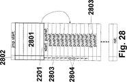
図28には、マイクロコントローラ制御におけるKRの構造が描かれている。まず最初にジャンプ命令がおかれており、これによってKRのヘッダ(2801)の後ろへのジャンプが行われる。各KWにはFILMOビット(2802)が割り当てられている。この場合、値1(2803)によって、KWがCELにより受け入れられ(ACCEPT)、次のスキャン時にはもはや実行されないことが表されている。値0(2804)はREJECTを表し、そのKWは次のスキャン時に新たに実行されなければならない。オプションとしてのKR統計(2701)は、0の付された最初のKWを指している。PUSHRET(2805)がREJECTを受け取ると、KRの処理はそこで中止され、次のスキャン時に最初のKWにおいてあるいは2701の指すロケーションにおいて新たに行われる。そうでなければ、KRはその終端で2806において規定どおりに終了する。
【0200】
図29には、FILMOスキャン前またはKRスタート前のCELのステータス情報を保護するための回路が示されている。このステータス情報は、CEL(2901)からレジスタ(2902)へ到達する。FILMOのスキャン前またはKRのスタート前、CTはイネーブル信号(2903)を2902へ送る。それに応じてステータス情報が引き継がれ、CTへ転送される(2904)。2904は、2903からの次の発信までそのまま一定に維持される。
【0201】
用語の定義
ACCEPT
アドレッシングされたCELがコンフィグレーション可能な状態にあり送られたKWを受け入れることを表す
ブロック命令(たとえばBLOCK−MOVE)
複数のデータ(ブロック)をメモリ内またはメモリと周辺装置の間でシフトさせる命令。この場合、シフトすべきデータの出所アドレス、そのデータの宛先アドレス、ならびにデータブロックの長さが表される。
【0202】
ブロードキャスト
多数の受信側への情報の送信
データ受信側
CELの結果を後続処理するユニット
データ送信側
CELのためのデータをオペランドとして利用できるユニット
データワード
1つのデータワードは任意の長さのビット列から成る。このビット列は、装置のための1つの処理単位を成している。1つのデータワードにおいて、プロセッサ等のコンポーネントのための命令も純粋なデータもコーディングすることができる。
【0203】
デッドロック
対向するブロックに起因していかなるデータ処理も不可能な状態
DFP
DE 44 16 881 によるデータフロープロセッサ
DPGA
ダイナミックにコンフィグレーション可能なFPGA。従来の技術。
【0204】
エレメント
あらゆる種類の完結したユニットに対する総称であって、部品として電子コンポーネント内で使用できるもの。つまりエレメントとは:
−あらゆる種類のコンフィグレーション可能なセル
−クラスタ
−RAMブロック
−ロジック
−算術ユニット
−レジスタ
−マルチプレクサ
−チップのI/Oピン
結果
ある結果は、使用に適した何らかのやり方でハードウェアにより評価することができ、その評価に対する反応として条件付けられたアクションをトリガさせることができる。
【0205】
したがって結果とはたとえば:
−計算装置のクロックサイクル
−内部または外部の割り込み信号
−コンポーネント内部における他のエレメントからのトリガ信号
−データストリームおよび/または命令ストリームとある値との比較
−インプット/アウトプットの結果
−カウンタのシーケンス、オーバーフロー、新たなセット等
−比較の評価
FIFO
従来技術によるファーストイン・ファーストアウト・メモリ
FILMO
リニアにデータの読み出される変形FIFO。メモリ始端への読み出しポインタの制限はない。
【0206】
FPGA
プログラミング可能なロジックコンポーネント。従来技術。
【0207】
F−PLUREG
CELの機能のセットされるレジスタ。ワン・ショットモード(OneShot-Mode)、スリープ・モード(Sleeo-Mode)もセットされる。
【0208】
フラグメンテーション
メモリが細分化され、たいていは小さくしたがって役に立たない多数のメモリ領域になること
ガーベージコレクタ
メモリ管理ユニット。フラグメンテーションを回避する。
【0209】
Hレベル
利用される技術に応じて論理値1のレベル
HOST
上位のコンピュータのコンポーネントまたはアセンブリ
IDLEサイクル
ステートマシンが処理を実行しないサイクル。ステートマシンの基本状態。
【0210】
Inter−CTバス
1つの平面における複数のCTと上位におかれたCT(CTグループ)間のバスシステム
INITIATOR
Inter−CTバスへのアクセスをスタートさせるCT
ポインタ
アドレスまたはデータワードへのポインタ
コンフィグレーション可能なエレメント(KE)
コンフィグレーション可能なエレメントは、専用の機能のためのコンフィグレーションワードにより形成可能なロジックコンポーネントのユニットを成している。したがってコンフィグレーション可能なエレメントは、あらゆる種類のRAMセル、マルチプレクサ、算術論理ユニット、レジスタ、ならびにあらゆる種類の内部および外部のネットワーク仕様等である。
【0211】
コンフィグレーション可能なセル(CEL)
ロジックセルを参照
コンフィグレーション
ロジックユニット、(FPGA)セルまたはCELの機能およびネットワークの形成(再コンフィグレーションを参照)。
【0212】
コンフィグレーションデータ
任意の量のコンフィグレーションワード
コンフィグレーションルーチン
複数のコンフィグレーションワードが1つのアルゴリズムにまとめられたもの コンフィグレーションメモリ
コンフィグレーションメモリには1つまたは複数のコンフィグレーションワードが含まれている。
【0213】
コンフィグレーションワード(KW)は任意の長さのビット列から成る。このビット列は、コンフィグレーションすべきエレメントに対する有効なセッティングを成しており、したがって機能を果たす1つの単位が生じる。
【0214】
ロードロジック
CELをコンフィグレーションおよび再コンフィグレーションsるためのユニット。特別にその役割に整合されたマイクロコントローラによって構成されている。
【0215】
ロジックセル
DFP、FPGA、DPGAにおいて用いられるコンフィグレーション可能なセルであって、コンフィグレーションに従い簡単な論理的または算術的役割で満たされる。
【0216】
ルックアップテーブル
従来技術。データの変換方法。
【0217】
LUT1
トリガをIDに変換するルックアップテーブルであって、トリガが有効なIDに割り当てられているか否かが判定される。
【0218】
LUT2
IDをローカルメモリ内の対応するKRのアドレスに変換するルックアップテーブルであって、KRがローカルメモリ内に存在しているか否かが判定される。
【0219】
Lレベル
利用される技術に応じて論理値0レベル
マスク
複数の信号のうち有効な信号を与えるビットの組み合わせ
RECONFIGトリガ
再コンフィグレーション可能な状態へのCELのセット
REJECT
アドレッシングされたCELがコンフィグレーション可能でない状態にあり、送られたKWを受け入れられないことを表す信号
REMOVE<ID>
1.IDにより参照されたKRを除去するためのKR内の命令
2.IDにより参照されたKRを消去するため、上位のCTから別個のインタフェースまたはハンドシェーキングを介して下位のCTへ送られる命令
RESET
コンポーネントまたはコンピュータシステム全体を規定された基本状態へリセットすること
ROOT−CT
外部のコンフィグレーションメモリへのダイレクトなアクセスを行う最高階層平面のCT
ラウンドロビン・アービタ
環状に進行し、最後に調停された信号に常に最下位優先順位を割り当てるアービタ。
【0220】
同期信号
コンフィグレーション可能なエレメントまたは算術ユニットにより生成され、データ処理の制御および同期合わせのため別のコンフィグレーション可能なエレメントまたは算術ユニットへ転送されるステータス信号。この同期信号を時間的に遅らせて(記憶して)、同じコンフィグレーション可能なエレメントまたは算術ユニットへ戻すこともできる。
【0221】
TARGET
Inter−CTバスへのアクセスの目標となるCT。
【0222】
トリガ
同期信号と同義語
再コンフィグレーション
任意の残量のCELが本来の機能を継続している間に任意の量のCELを新たにコンフィグレーションすること(コンフィグレーション参照)。
【0223】
チェーンリスト
ポインタによってつなぎ合わせられた従来技術によるデータ構造
セル
コンフィグレーション可能なエレメントと同義語。
【0224】
ステートマシン
様々な状態をとり得るロジック。各状態間の移行は、種々の入力パラメータに依存する。このマシンは複雑な機能を制御するために用いられ、従来技術に相応する。
【図面の簡単な説明】
【図1】 ルックアップテーブル内におけるアドレッシング方法を示す図である。
【図2】 ステートマシンの命令処理と機能を示す図である。
【図3】 ステートマシンの命令処理と機能を示す図である。
【図4】 ステートマシンの命令処理と機能を示す図である。
【図5】 ステートマシンの命令処理と機能を示す図である。
【図6】 ステートマシンの命令処理と機能を示す図である。
【図7】 ステートマシンの命令処理と機能を示す図である。
【図8】 SCRR−ARBの構造を示す図である。
【図9】 LUT1&LUT2の構造を示す図である。
【図10】 ポインタ演算装置とCTRの構造を示す図である。
【図11】 FILMOの構造を示す図である。
【図12】 図12のaはCTの階層構造を示す図であり、図12のbは各CT間におけるトリガの送信を示す図であり、図12c,dは送信方法を示す図である。
【図13】 複数のIKRによるKRの呼び出しを示す図である。
【図14】 ROOT−CTにおけるLUT1の構造を示す図である。
【図15】 ROOT−CTにおけるHOSTコントロールの構造を示す図である。
【図16】 LUTとECRのコンセプトを示す図である。
【図17】 中間階層平面ないしはROOT−CTにおけるCTのシーケンスコントロールを示す図である。
【図18】 2次元アレイのコンフィグレーションにおけるデッドロックの問題点を示す図である。
【図19】 FILMOコンセプトを示す図である。
【図20】 Inter−CTコミュニケーションの基本原理を示す図である。
【図21】 GETCTS方式によるInter−CTコミュニケーションの実装例を示す図である。
【図22】 GETBUS方式によるInter−CTコミュニケーションの実装例を示す図である。
【図23】 Iter−CTバスのバス構造を示す図である。
【図24】 CT階層内におけるアドレッシングを示す図である。
【図25】 ガーベージリストである。
【図26】 KR内のFILMO機能を示す図である。
【図27】 FILMOリストである。
【図28】 KRまたはFILMOを実行する前の状態の格納について示す図である。
【図29】 FILMOスキャン前またはKRスタート前のCELのステータス情報を保護するための回路を示す図である。[0001]
Background of the Invention
Conventional technology
The prior art on which this application is based is based on patent application 196 54 846.2-53 (Data Flow Processor (DFP) with two or more dimensional programmable cell matrices (FPGA, DPGA, etc.) and component self-supporting) Dynamic Reloading Method), as well as patent application 196 54 593.5-53 (Method for Reconfiguring Components Programmable at Runtime). It describes how to configure and reconfigure DFP and similar components according to FPGA, DPGA and prior art, according to which a component similar to a microcontroller formed separately and centrally located at the top It is responsible for the distribution of fairly passive control units located in the subordinates.
[0002]
problem
Using a central global unit that controls the reconfiguration of each part of one or more components (eg cells (CEL)), when many different reconfiguration requests must be processed at once It becomes a Kushiro. The advantages of the parallelism of the aforementioned components are limited by the central unit as described above. Because they constitute a typical “bottleneck”, this greatly slows down data processing. Furthermore, the assignment of event sources to the configuration to be loaded becomes a problem. This is because the operation is performed with the absolute address of the configuration memory. The reconfiguration unit must therefore include a kind of memory management system, which records which memory areas are used by which configuration, as in the case of the operating system. An additional problem is the management of resources (eg CEL). In this case, it must be ensured that each CEL (cell) is only given exactly once to the algorithm that was started by the reconfiguration request and also uses the remaining peripheral CEL. Otherwise, deadlock may occur.
[0003]
To clarify the problem of reconfiguration once again, the following example is given. One matrix of multiple CELs is not configured and is in the RESET state. Each CEL can represent whether they are in a reconfigured state. All CELs in the matrix are in a standby state for configuration, i.e., in a reconfigurable state. The first configuration routine (KR1) is loaded, in which case the matrix is not fully used. The configured CEL turns off the cue that it is in a configurable state. A second configuration routine (KR2) independent of the first configuration routine is loaded into a group of CELs that have not yet been configured. In this case, the third configuration routine cannot be loaded. Because these cells are required for the first and / or second configuration routines, they are used and not in a configurable state. KR3 must be stopped until the required CEL is released, that is, until KR1 and KR2 have ended. During the execution of KR1 and KR2, further load requests for the fourth configuration routine (KR4) and the fifth configuration routine (KR5) occur, but they cannot all be executed immediately. Because they utilize the CEL used by KR1 and KR2. KR3 and KR4 partially use the same CEL, but KR5 uses neither KR3 nor KR4 CEL.
[0004]
The request to redo KR3 to KR5 in order is as follows:
1. Load KR3 to KR5 so that the temporal order is maintained as much as possible according to the load request.
[0005]
2. To maintain maximum parallelism, load as many KRs as possible without depending on each other, ie without having a common CEL.
[0006]
3. Each KR must not block each other. In other words, KR3 is partially loaded, but cannot be loaded any further because other CEL is blocked by partially loaded KR4. On the other hand, KR4 cannot load any more. This is because the similarly required CEL is blocked by KR3. This causes a typical deadlock condition.
[0007]
4). It is impossible for the compiler that generated the KR to identify the execution of the KR that overlaps in time and resolve the conflict state.
[0008]
In this case, the relationship between the cost of the circuit to be realized and the optimum result must be as good as possible. In other words, the object of the present invention is to enable a flexible, parallel and deadlock-free configuration at the lowest possible cost, and to execute it with little time and computational effort. Is to do. In this case, you must solve the following basic problems:
If only -K3 is loaded, deadlock does not occur in that way, but it is not optimal because KR5 could also be loaded.
[0009]
-If KR3 is loaded and KR4 is not loaded, KR5 must pre-record KR4 so that it has the highest priority for the subsequent loading process, which can be very administratively intensive Means.
[0010]
A deadlock free state is obtained by the method described below:
Improvements and problems of the present invention
The basic problem of the present invention is to construct a unit (hereinafter referred to as a configuration table CT) that has a hierarchical structure and can appear many times at each level. The level is reduced from the lowest hierarchical level to the highest hierarchical level so that exactly one CT exists at the upper level. Each CT configures and controls a plurality of configurable elements (CEL) independently of other parallel CTs. The CT in the higher hierarchy can temporarily store the configuration routine for the CT placed in the lower hierarchy. If multiple CTs located in a lower hierarchy require the same configuration routine, the routine is temporarily stored in the CT located in the higher hierarchy and is called from an individual CT. In this case, the CT placed in a higher hierarchy only calls the corresponding configuration routine once from the global common configuration memory, thereby achieving a cache effect. Apart from configurable components, the present invention can be used as a cache method for instruction and data caches in a microprocessor, DFP or equivalent with multiple computing mechanisms. In this case, some of the units described below (for example, FILMO) can be omitted depending on the application, but the hierarchical structure is basically not changed. This usage is therefore considered a subset and will not go into further detail. A significant advantage of the method described here over conventional caching methods is that data and / or code is cached selectively, that is, based on a method that is precisely tuned to the algorithm. Furthermore, according to the present invention, it becomes possible to reconfigure a large cell structure completely without deadlock.
[0011]
Description of the invention
Instead of consolidating a central global unit into a single component that handles all configuration requests as in the past, according to the present invention, it can play its role and is arranged in a hierarchical structure (tree structure) A plurality of active units are provided. At that time, the request from the lowest level (leaf in the hierarchical structure) is transferred to the next higher hierarchical level only when the request cannot be processed. These steps are repeated for all existing levels until the highest level is reached. The highest level is connected to an internal or external configuration memory located at a higher level, and includes configuration data that is required for execution of the program at some time.
[0012]
A kind of caching for the configuration data is achieved by the tree structure in the configuration unit. Access to the configuration is mainly local. As the most disadvantageous situation, when the corresponding data does not exist in any of the CTs arranged in a hierarchical structure, it is necessary to load the configuration from the configuration memory located at the upper level. In doing so, deadlocks are avoided by incorporating a fixed time sequence for the configuration to be loaded and consolidating the configuration into one list. The CEL status information is protected before loading, so that it remains unchanged while the entire list of configurations is used.
[0013]
CT basics
The configuration table (CT) is an active unit that responds to a synchronization signal, the so-called trigger. This trigger is a two-dimensional or higher dimensional matrix consisting of a plurality of electronic components (hereinafter referred to as configurable elements CEL) for conventional arithmetic or logic units, address generators, arithmetic units, etc. Generated. Based on the trigger that occurs, a predetermined action is triggered in the CT. In this case, the role of the CT is to take over control of the plurality of CELs and obtain their arithmetic and / or logical operations. In particular, the CEL needs to be configured and reconfigured. CT plays this role, which manages a plurality of possible configuration routines (KR), each consisting of a plurality of individual configuration words (KW), and a plurality of CELs based on the trigger condition as one of the KRs. This is done by configuring one or more. At that time, each CEL includes one or more configuration words, and this is provided with the address of the CEL to be configured. In this case, the KR must be copied completely and properly to a plurality of CELs, where the plurality of CELs can be grouped into groups configured by different but completely executed KRs. At that time, all the CELs are connected as follows within the group. That is, after confirming the required reconfiguration, each CEL must finish data processing and shift to a state where reconfiguration is possible by a common signal (ReConfig) for all grouped CELs. It is connected in the group so that it is notified.
[0014]
Basics of reconfiguration without deadlock
A problem that arises in a system that is reconfigurable at runtime is that each time two parts wait on each other, so the system can fall into a deadlock situation.
[0015]
These problems can be avoided by making sure that the new configuration is always loaded into the system or not at all, or by applying a kind of timeout method. However, this causes a series of drawbacks (required space, propagation time, etc.) and problems. For example,
-What to do if the configuration cannot be loaded
-Managing the order in which configurations are loaded
-In some cases, there is a drop in performance because other configurations that might be able to be loaded into the CEL are not noted.
Etc.
[0016]
According to the method described below, these problems can be eliminated. This starts from a DFP system according to the prior art.
[0017]
A trigger signal is sent from a certain CEL to the CT. This CT locates the trigger source and selects the configuration (KR) to be loaded by a lookup table. Incoming trigger signals are blocked and no other triggers are accepted until the current configuration has been completely processed. One configuration consists of a plurality of instructions, which are transmitted to a set of CELs. However, in a system that can be configured at propagation time, there is no guarantee that any configuration command (KW) can be executed. This may fail, for example, because the addressable configurable element (CEL) still does not finish its task and therefore cannot receive new configuration data. All configuration instructions that failed to execute (because the corresponding CEL was not in a reconfigurable state and rejected the configuration (REJECT)) to avoid performance degradation, according to the FIFO (detailed below) It is written after the last configuration instruction existing in the dedicated memory (FILMO). The next configuration instruction is then processed in the same way. This is repeated until the end of one configuration is reached.
[0018]
The CT then goes back to accepting the trigger signal to allow another configuration to be loaded in some cases. In this state, CT processes FILMO at regular intervals by timer control.
[0019]
Prioritization of the configuration to be loaded is performed by the CT passing through the memory FILMO before the configuration to be originally loaded is processed. A FIFO-like FILMO structure automatically ensures that KWs that could not be completely processed during the previous trigger request have a higher priority than WKs to be newly processed. In processing the memory (FILMO), each configurable element (CEL) addressed by a configuration command is tested for whether it is in the state “configurable” before or during transmission of the KW. In this state “configurable” (ACCEPT), data is transmitted and erased from the memory FILMO. If it is in the state “non-configurable” (REJECT), the data is left in FILMO and is newly processed at the next scan. CT processes the next entry in FILMO. This is repeated until the end of FILMO is reached. Thereafter, the original configuration activated by the generation of the trigger signal is processed. In this case, the FILMO structure corresponds to the FIFO method, that is, the oldest entry is processed first. For the purpose of processing FILMO even if no new KR is loaded, FILMO is scanned at regular intervals by timer control.
[0020]
Other configurable elements (CEL) that are not involved continue to be processed in parallel during this phase and their function is not affected. This can lead to a situation where one or more configurable elements (CEL) transition to the state “configurable” while the CT is processing the FILMO. Since CT can be in a processing state at any point in FILMO, the following situations can occur:
The CT attempts to process the first instruction whose addressed configurable element (CEL) is not in the state “configurable”. This causes the CT to continue with the next command (KW). At the same time, one or more configurable elements transition to the state “configurable”, including configurable elements that may have been written by the first configuration instruction. The CT processes a second configuration instruction (KW), which uses a configurable element (CEL) that is the same as the first configuration instruction, but from another configuration. At this point, the configurable element (CEL) is in the state “configurable” and can successfully process the instruction.
[0021]
This no longer guarantees that the configuration to be loaded first is actually finished first. In this case, there may be two partially completed configurations, each of which requires a configurable element of the other configuration in order to be fully loaded. Here a deadlock condition occurs, which is illustrated in FIG. In this case, configuration A and configuration B are to be configured. The CT has already loaded the hatched parts in Configuration A and Configuration B. Configuration A further requires a bright and double hatched area of Configuration B for completion, and Configuration B requires a dark and double hatched area of Configuration A for completion. I need. Both of these configurations are not yet completely complete, and therefore have no ability to perform a function, so for both configurations one of these two configurations will be removed in the final state. not enter. Both of these configurations are waiting for configurable elements that are still needed to be released.
[0022]
In the case of the method according to the invention, deadlock is avoided as follows. That is, the CT captures the state of all configurable elements prior to processing the FILMO and accordingly no longer allows any changes until the event ends, i.e. ignores the changes that occur. In other words, the state of all configurable elements is protected before FILMO processing, or state changes are prevented during FILMO processing. One feasible technical form is to use one register in each configurable element and protect that register with the state prior to FILMO processing. CT operates based only on the captured state and does not operate depending on the current state of the configurable element. This ensures that the instruction (KW) to be processed can find the same state of the configurable element (CEL). This step does not preclude the transition of one or more configurable elements to the state “configurable” during FILMO processing. This change is not immediately visible to the CT during processing, but will be noticed only at the start of the next execution.
[0023]
Configuration order
What is absolutely necessary for the configuration of a given algorithm is to keep exactly the order in which the KWs are written to the CEL. For example, it is useful to configure the bus system first before connecting the CEL to the bus system, thereby preventing the CEL from being connected to the bus used by other routines. In other words, the CEL is configured only when the corresponding bus connection can be configured in advance.
[0024]
In the case of the method according to the invention, a fixed order adherence is achieved as follows:
A configuration word (KW) having an important structure for the subsequent KW configuration is specially represented (hereinafter referred to as KWR). If such KWR configuration fails, all subsequent KWs in the corresponding configuration routine (KR) are written to FILMO and are not executed in this process. Even during a FILMO scan, all KWs that are behind the KWR and failed to be configured are not executed in the current process.
[0025]
Caching method
The CT structure is a hierarchical structure, that is, a plurality of CT levels exist in one component. This arrangement advantageously corresponds to a tree structure (CT tree). In this case, the root CT (Root-CT) is an external configuration memory (ECR), in which all KRs are stored in association with each other, while a configurable element (CEL) is stored in the leaf. Are associated with each other, thereby calling individual KRs. Each intermediate level CT is associated with a configurable element, which is placed in the same hierarchical level. Each CT is associated with a local internal memory. This memory is partially erased when there is no more space for a KR to be newly stored, or when it is explicitly requested by a special CT instruction (REMOVE). In this case, erasure is performed for each KR according to the erasure criteria so that, at best, only those KRs that are no longer required or only those KRs explicitly expressed by the REMOVE instruction are erased. Similarly, KRs are erased one by one so that only the number of memories necessary to write a new KR to be loaded into the memory, that is, the necessary number of memories is freed. As a result, as many KRs as possible can be left in the memory to optimize the cache effect.
[0026]
The advantage of this is that each CT placed under any CTx, that is, a CT that is far above in the CT tree, requests a KR that is not stored in CTx from the external configuration memory ECR. Instead of receiving directly from CTx. This creates a cache structure across multiple levels. The complexity of data transmission in the CT tree, especially the required memory bandwidth in the ECR, is significantly reduced.
[0027]
In other words, each CT buffers the KR of the underlying CT. That is, the CT located at the lower side receives the necessary KR directly from the CT located at the upper side, and memory access to the external ECR is not required. The KR need only be loaded via access to the ECR only when the required KR is not present in any of the higher CTs. This provides a particularly efficient hierarchical cache structure for KR. An erasure criterion that can be realized based on this structure is also obtained, but this is determined empirically depending on the application. Here are some possibilities:
-Erase the oldest entry
-Erase the smallest entry
-Delete the largest entry
-Erase the rarely called entry
Basics of CT hierarchy
To achieve the cache effect, CTs are organized into a hierarchy in the tree structure. There is a bus system (Inter-CT-Bus) between the individual nodes (CT), which connects an upper node (CT) with a plurality of lower nodes (CT). At that time, the lower node (CT) requests data from the upper node (CT), and the upper node sends data to the lower node accordingly. Lower nodes exchange status information with each other, so that networks between higher nodes are used, and those networks need to resolve addresses accordingly.
[0028]
CT hierarchy and addressing
The CT hierarchy is arranged so that a binary tree can be used for addressing individual CTs. That is, the least significant address bits represent individual leaves of the tree, and each other address bit selects one hierarchical level above. Therefore, each CT has a unique address.
[0029]
The table below shows how the individual address bits are assigned to the individual levels.
[0030]
[Table 1]
* = Address bits used
-= Unused address bits
When an upper CT is assigned to a group consisting of a plurality of CTs, the plurality of address bits in that group are grouped accordingly.
[0032]
The following table shows how individual address bits are assigned to individual levels, where there is a group with 8 CTs at level 0 (address (Bit 2.0)
[0033]
[Table 2]
* = Address bits used
-= Unused address bits
The structure of the binary tree can be done in one dimension or in multiple dimensions, which is done by forming one binary tree for each dimension.
[0035]
A specific CT (TARGET) is addressed, which is either the starting CT (INITIATOT) points to the correct target address, or the TAGET is relatively addressed.
[0036]
Next, the relative address evaluation is explained in detail:
An example of a relative address field for two-dimensional addressing:
[0037]
[Table 3]
Bit 15 is set when the next higher level CT is to be selected. Bit 14 also represents a broadcast, thus selecting all CTs. The X / Y address represents a TARGET address starting from the INITIATOR address.
[0039]
The address is a signed "signed" integer. TARGET is obtained by adding the Y / X address of the address field to the current address position. Each level has a specific address width. The adder corresponds to this width.
[0040]
An overflow or underflow in the addition means that the addressed CT is not located below the current node, and the address request is transferred to the CT above it (the next highest node). Means that. If no overflow or underflow occurs, TARGET is positioned below the current node. The address bits calculated at the current level (see table) select the CT located immediately below the current node. The next lower CT (node) is then selected based on the correspondingly calculated address bits.
[0041]
Prioritizing access in CH hierarchy
Access to the internal CT bus is managed by the arbiter. In this case, equal priority is given to all lower nodes. The upper node has a higher priority. Thereby, an access transmitted from an upper node to a lower layer, or an access that has already advanced considerably from INITIATOR is given priority over other accesses.
[0042]
Basic structure of CT
We will get an overview of the individual components from the following overview of CT. Below, each component is demonstrated in detail.
[0043]
The core of the CT is the control state machine (CTS), which controls all processing of the configuration routine (KR). Each CT is assigned a garbage collector (GC), which controls the removal of KR from the CT's memory (CTR). Note that FILMO is still responsible for managing KW to be processed, and the LOAD state machine controls the loading of KR.
[0044]
The memory (CTR) is configured as a conventional write / read memory, in which all technically possible implementations can be applied, with the KR for the individual CT and the subordinate CTs being applied. Used for local storage. As a special case, the memory (CTR) can be configured as a ROM, EPROM, EEPROM, flash ROM or the like for the purpose of providing a component with a function similar to ASIC or PLD (refer to the prior art).
[0045]
A number of pointers configured as loadable counters are used to generate CTR addresses:
1. Free pointer (FP). This points to the first free memory location after the last KR in the CTR.
[0046]
2. Garbage pointer (GP). This refers to the entry to be removed from the CTR by the garbage collector (GC).
[0047]
3. Move pointer (MP). The memory location in the CTR that this points to is the location where the final configuration word (KW) or KR entry that should not be removed is copied / moved from that position to the entry defined by the GP.
[0048]
4). Program point (PP). This refers to the KW currently being executed by the CTS.
[0049]
KW is transferred to the CEL to which it belongs via the output interface (OUT). CEL acknowledges receipt of KW as long as it is in a configurable state (ACCEPT). If the KW is rejected (REJECT), it is temporarily buffered in a memory similar to a FIFO (FILMO) for later writing to the addressed CEL again without using the program pointer .
[0050]
The CTS receives a request for processing the KR by a trigger signal. This trigger signal passes through a mask, which is a filter that filters out unwanted masks. In accordance with the prior art, the mask can be configured with an AND gate (AND), which causes the trigger and the enable signal to be ANDed. The trigger is converted to a binary signal via a prioritized round-robin arbiter (SCRR-ARB). The prioritized round-robin arbiter combines the benefits of round-robin arbiter equality with the detection of the next enable within a clock or priority-arbiter.
[0051]
The masked trigger is supplied as an address to the first lookup table (LUT1), which assigns the ID of the corresponding KR to the incoming trigger as an address and sends it to the data line. In the second lookup table (LUT2), the KR ID is assigned to the address of the KR memory location in the CTR. The second look-up table is used not only for assigning trigger signals, but also for assigning addresses for instructions that use ID as a parameter. The correspondence between the trigger signal and the corresponding ID is entered in the
[0052]
The following are the basic instruction sets that can be implemented to better understand CT:
1. BEGIN <ID>
BEGIN <ID> represents the start of the configuration routine. <ID> represents a unique identification number in the configuration routine.
[0053]
2. STOP
STOP represents the end of the configuration routine. At this position, the configuration table (CT) ends the processing of the configuration routine. The garbage collector (GC) finishes removing the entry in its configuration routine.
[0054]
3. EXECUTE <ID>
Jump to the beginning of the configuration routine (BEGIN <ID>). If this routine does not exist in the CT's memory, it is requested or loaded from memory for the CT located above it.
[0055]
4). LOAD <ID>
KR <ID> is requested for the CT located above it.
[0056]
5. REMOVE <ID>
Call GC. The purpose is to remove the configuration routine <ID> from the CT memory from BEGIN <ID> to STOP until the configuration routine removed no longer creates a memory gap. To push forward.
[0057]
6). PUSH <FORCED><ADDRESS><DATA><EXIT>
Write configuration data <DATA> to register <ADDRESS>. If <FORCED> is set, data is written even if the RECONFIG flag of the corresponding target register is not set. <EXIT> is used to indicate that it is a KWR that stops the subsequent execution of the subsequent KWR during REJECT.
[0058]
7). MASK <SR><TRIGGER>
Depending on <SR> (Set / Reset), the trigger mask is set by <TRIGGER> or reset by <TRIGGER>.
[0059]
8). WAIT <UNMASKED><TRIGGER>
The processing of the configuration routine is stopped and a trigger <TRIGGER> is waited for. If <UNMASKED> is set, it responds to the waiting trigger regardless of the state of the trigger mask.
[0060]
9. Trigger <TRIGGER><CT#>
The binary value of the trigger is sent to the upper CT addressed by CT #.
[0061]
Ten. GETBUS / GETCTS
Establish a connection to the internal CT bus.
[0062]
11. LOOSEBUS / LOOSECTTS
Release the connection to the internal CT bus.
[0063]
12. REFERENCE <TRIGGER><ID>
The value <ID> is written to LUT1 at the address <TRIGGER>, thereby assigning a specific KR to the trigger signal.
[0064]
Instructions EXECUTE, LOAD, REMOVE, PUSH, MASK, WAIT, TRIGGER, REFERENCE are BEGIN and. . . It is valid only within the STOP. Outside this group, no instruction is executed.
[0065]
The structure of the configuration routine (KR) is as follows:
BEGIN <ID>;
. . .
Valid instructions
. . .
STOP;
Indirect addressing (reference)
The CT cache principle allows KR buffering within the CT, where KR is used by different CTs or CELs located below. When accessing the external interface of a component (eg, RAM, peripheral device) from a lower unit, it is necessary to store various addresses or portions of the external interface. This will basically distinguish the contents of the individual KRs that are required. Caching is no longer possible. In this case, measures are taken by indirect reference. A dedicated KR (hereinafter referred to as IKR) is used for this purpose, which has the necessary external parameters and sets it. Other different KRs at different hierarchy levels are invoked via triggers as needed. The original KR is called from the end of the IKR. Only the IKR cannot be cached, while the called KR is completely unique and is therefore cacheable. It is useful here to reduce the size of the IKR to an absolute minimum, i.e. exclusively to different external parameters and the original KR call.
[0066]
The indirect configuration routine (IKR) is structured as follows:
BEGIN <ID>;
. . .
xxx; valid instructions, in this case only controlling external peripherals
TRIGGER <ID>; Start, stop or load request to peripheral process
. . .
GOTO <ID>; Jump to the original KR
STOP;
Special case:
1. WAIT_FOR_BOOT
This instruction is valid only for the first address of the CTR. During the boot process, the complete boot KR is first written to the CTR, but it is not the boot-KR BEGIN <0> start sequence. There is WAIT_FOR_BOOT at that location (address 1), which is automatically set at RESET. Only after the entire Boot-KR is written to the CTR, WAIT_FOR_BOOT is overwritten by BEGIN <0>, and the CTS starts the Boot-KR process. WAIT_FOR_BOOT must not appear in the program.
[0067]
2. BOOT <CT-ID>
BOOT <CT-ID> represents in which CT the subsequent Boot-KR should be written. BOOT <CT-ID> is not followed by BEGIN, and Boot-KR ends with BOOT <CT-ID> that follows, not with STOP. Then, the boot process is terminated by STOP. BOOT <CT-ID> must not appear in the program.
[0068]
Boot process
After RESET, the CT of the highest hierarchy level (ROOT-CT) loads Boot-KR into the CT of the lower hierarchy. For this purpose, there is a jump to a defined address (BOOT-ADR) in an external configuration memory (ECR) associated with the ROOT-CT. The ROOT-CT performs this jump and reaches the boot sequence. This is structured as follows:
BOOT <CT-ID0>;COMMAND;COMMAND; . .
BOOT <CT-ID1>;COMMAND;COMMAND; . .
. . .
BOOT <CT-IDn>;COMMAND;COMMAND; . .
STOP;
During the boot process, the entire Boot-KR is first written into the CTR from address 2 of the CT represented by <CT-ID>. The start sequence of Boot-KR (BEGIN <0>) is not written to address 1. At that location is WAIT_FOR_BOOT, which is automatically set at RESET. Only when the entire Boot-KR is written to the CTR, the ROOT-CT reaches the next BOOT <CT-ID>, the STOP is written to the CTR at the end of the Boot-KR, and the WAIT_FOR_BOOT is overwritten by the BEGIN <0> The The CTS starts the Boot-KR process.
[0069]
Load configuration routines
There are three basic mechanisms for requesting configuration routines outside the Boot-KR.
[0070]
1. Execution of LOAD <ID> by CTS
2. Execution of EXECUTE <ID> by CTS, KR having the corresponding ID does not exist in the CTR.
[0071]
3. Generation of a trigger, which is converted to <ID> via LUT1, and the KR belonging to it does not exist in the CTR.
[0072]
The progress in all three cases is the same:
The requested KR ID is supplied to LUT 2 as an address. LUT2 checks whether a valid address exists in the CTR. If this does not exist, that is, if <ID> points to the
[0073]
In response, the CTS requests a KR corresponding to <ID> in the CT that is hierarchically higher. This request reaches the upper CT in the form of a trigger and is evaluated accordingly. The upper CT sends the requested KR to the requested CT. Data is written into the CTR from the address pointed to by FREE-POINTER (FP), where FP is incremented by 1 for each write access. When the FP reaches the upper limit of the CTR, the garbage collector (GC) is called, and the lowest KR in the CTR is removed and the CTR is compressed. At that time, FP is newly set. This process is performed until the KR to be loaded is completely in the CTR.
[0074]
Jump table in configuration memory
The configuration memory assigned to the ROOT-CT contains the entire KR that must be loaded for the application. In the external configuration memory (ECR), a jump to the boot configuration routine is placed at a predetermined address (ARD-BOOT). Jumps to individual KRs are placed in another predetermined memory area (LUT-ECR), which is optional but has a fixed length within the application. In this case, the <ID> of the individual KR is used as an address in the ECR, where there is the start address of the individual KR. This indirectly addresses the KR:
ID->LUT-ECT-> KR
KR change in configuration memory
The KR with ID <A> will be changed. First, HOST writes a new KR for ID <A> to an empty memory location in the ECR. ID <A> is written in the ROOT-CT register provided for this purpose together with the new address of KR in the configuration memory in the host unit (HOST). ROOT-CT sends the command REMOVE <A> to all CTs below it. In response, all CTs remove the KR associated with that ID from the CTR when STOP is reached or during the IDLE cycle, ie, if KR is not executed, and LUT2 sets "NoAdr" to address <A>. set. That is, this means that there is no valid address entry for ID <A> in LUT2. If ID <A> is requested again, the missing entry ("NoAdr") is not forced to <A> to LUT2, and each CT requests a new KR <A> from the ECR.
[0075]
FILMO
KR mainly consists of the instruction PUSH, which writes a new configuration word at a given address. If the addressable configurable element (CEL) is not ready to accept a new configuration (REJECT), and if it is not possible to write a type KW configuration word, the configuration word is addressed Instead of a configurable element (CEL), it is written into a memory called FILMO below. Subsequent instructions are processed normally until the configuration word cannot be written again, otherwise the word is written to FILMO.
[0076]
If the addressable configurable element (CEL) is not ready to accept a new configuration (REJECT), and it is not possible to write a configuration word of type KWR, the configuration word is addressed Instead of a configurable element (CEL), it is written in a memory called FILMO in the following. All subsequent instructions until KR ends are written directly to FILMO, not CEL.
[0077]
FILMO is scanned during the IDLE cycle and before each new KR is executed. In this case, starting with the oldest data word, each word of the read FIFO is sent to the addressed element according to the FIFO according to the prior art. The element addressed here must already be ready to receive a configuration word. As long as the data word can be written from the beginning (ie, if the addressable configurable element (CEL) is in standby), the entry is removed from the FILMO in the form of a FIFO. If the configuration word cannot be written, it is skipped and not removed from FILMO. Unlike the FIFO, the post-configuration data that has been skipped is further read. The configuration word that can be written after the skipped configuration word is as follows according to the implementation of FILMO. That is,
1. Marked as written and not erased from FILMO. The configuration word marked here as written is no longer read in subsequent scans or is immediately erased if the skipped configuration word no longer exists before it.
[0078]
Or
2. Erased from FILMO. In this case, the configuration word is obtained as it is before and after the erased configuration word, where the subsequent word is shifted forward (upward) or the previous word backward (downward) for erasure, At that time, the order of the configuration words is compulsorily maintained.
[0079]
When a new KR is executed, a configuration word (KW) that could not be written to the addressed element (CEL) by the CTS is newly added to the FILMO, that is, KW is the FILMO (in the read direction). Finally written. When FILMO is full, i.e. there is no free entry for the configuration value, KR execution is stopped. FILMO can write enough configuration words and is scanned accordingly until a number of free entries occur, after which KR continues to be processed. FILMO has a FIFO-like memory that is always scanned linearly from the oldest entry. However, unlike the FIFO, the entry is skipped (First In Linear Multiple Out).
[0080]
Configuration table-State machine (CTS) functions
The configuration table state machine (CTS) plays a role of CT control. This executes the KR command and responds to incoming triggers. This then plays the role of managing FILMO, especially during the idle cycle, reading it before executing KR. This responds to signals illegal <TRG> (Illegal trigger, see 0102 in FIG. 1) and load <ID> generated by the LUT structure. The load <ID> is generated when a cache miss occurs in the LUT 2 (0105) or when the KR / IKR referred to by the ID is marked as deleted (0107). This responds to the upper CT control signal. 2-7 depict examples of implementations for instruction processing.
[0081]
Control signal to upper CT
-Illegal <TRG> (0102)
The upper CT indicates that an unknown trigger <TRG> has occurred.
[0082]
-Load <ID> (0105/0107)
Request to load <ID> from higher-level CT
-Trigger <TRG><CT#> (0108)
Send trigger <TRG> to higher CT or addressed CT <CT #>
Upper CT control signal
-Remove <ID> (see FIGS. 15 and 1513)
Request deletion of <ID> from CT
-Write_to_FP <data> (see FIG. 2, 0205)
Send data to CT. Data is appended to the end of the occupied memory.
[0083]
Garbage collector (GC) functions
There are two problems with CTR:
1. If the LOAD or EXECUTE instruction or trigger points to the ID of a KR that does not exist in the CTR, the KR must be reloaded. However, in some situations, there is not enough space in the CTR to load the requested KR.
[0084]
2. When REMOVE <ID> occurs, the corresponding KR must be removed from the CTR. In this case, if KR is not at the end of the CTR, a gap is generated. Even if a new KR is loaded, this gap may not be completely filled in some cases, or this gap may be too small for the new KR. As a result, CTR fragmentation occurs. The role of the garbage collector is to remove the KR from the CTR and to secure a space for a new entry, and to store the CTR after the entry removal as a block closed by all remaining KRs. The empty memory block is positioned at the end of the CTR as a closed block. This allows a new KR to be loaded optimally and without loss of memory location.
[0085]
Trigger pulse evaluation
Each CT has contacts for a plurality of trigger signals belonging to their individual hierarchical planes, and these trigger signals are sent to one bus to be collected. Incoming triggers are evaluated through a mask, ie an enabled trigger signal is transferred. The enabled trigger signal is buffered (sampled) in the sample register in synchronization with the clock. The arbiter selects one of the stored trigger signals and converts the signal to a binary vector. The selected trigger signal is erased from the sample register. The binary vector is transferred to the first look-up table (LUT1), and the binary vector is converted into the identification number (ID) of the configuration routine (KR) to be called by this table. The ID is converted into the address of the KR in the CT memory (CTR) in the second lookup table (LUT2). The CT state machine (CTS) sets its program pointer (PP) to the above address and starts executing KR. The assumption here is that each trigger enabled via the mask has a corresponding entry in LUT1. If this is missing, an error condition is transmitted to the CTS (Illegal trigger), where each ID = "NoAdr" is evaluated as a nonexistent entry. “NoAdr” is a token selected depending on the implementation. If there is no entry in the LUT 2, that is, if no KR corresponding to the ID exists in the CTR, a load request is sent to the CTS (load <ID>).
[0086]
Transmission of trigger pulse to upper CT
In addition to the previously described interface to the higher-level CT for loading the KR, there is another interface for exchanging trigger vectors, although it can be arbitrarily defined. At that time, CT
-Send command to all other CTs (BROADCAST)
-Or send an instruction to any addressed CT (ADDRESSED)
The instruction “Triggervektor” represents a binary value, which refers to an entry in LUT2 in the received CT. The transmission of the trigger vector is required, for example, to start the KR in a further CT within the IKR, thereby controlling eg peripheral devices and memory.
[0087]
There are two mechanisms for transferring the trigger vector to the upper CT.
[0088]
1. One bit is added to LUT1, which indicates whether the contents of the memory are considered a KR ID or a binary value of the trigger pulse. If a trigger pulse has occurred, the data contents of LUT1 are sent as they are to the host CT as a trigger.
[0089]
2. The trigger TRIGGER can represent the binary value of the trigger, which is sent as it is to the higher-level CT (alternatively, the ID may be transmitted as it is instead of the trigger value).
[0090]
In order to start KR in an unknown CT via a trigger vector, it is necessary to create a synchronization scheme so as not to cause a deadlock situation. With this scheme, care must be taken that only KRs in a particular group of CTs start another KR in other CTs in this group. If a plurality of KRs are started at the same time, deadlock may occur between the CTs as in the deadlock described above in the CEL plane.
[0091]
The basic principle of such a scheme proceeds as follows:
The KR is structured as follows:
. . .
GETCTS / GETBUS
TRIGGER <ID>, <CT #>
TRIGGER <ID>, <CT #>
. . .
LOOSECTTS / LOOSEBUS
. . .
This indicates that another CT (TAGET) is sent in the subsequent signal by the instruction “GETCTS” in the KR in CT (INITIATOR). With the triggers <ID> and <CT #>, the ID of the KR to be started is sent to a CT having a unique ID CT #. In this case, the transmission of the trigger is first made immediately to the upper CT, which in turn sends the trigger to the lower CT in the CT space, or to the upper CT for that CT space. Send (see CT hierarchy). If the order arrives, it confirms receipt.
[0092]
As instructions are executed by CT, the priority identifier of the instruction is increased by one each time. If an instruction transfer request hits another request in the CT, the instruction with the lowest priority is withdrawn.
[0093]
This guarantees the following:
[0094]
a) Only one instruction is propagated at some point in the overlapped system, so only one KR is started, which gives the situation without the required deadlock. .
[0095]
b) Instructions that have not been propagated to the farthest are dropped, which can improve performance. After the withdrawal of the instruction, all preceding instructions in GETCTS / LOOSSECTS are similarly dropped, that is, INITIATOR sends the signal DISMISS to all TARGETs and KR execution begins after the GETCTS wait time. Instruction section GETCTS. . . Acknowledgments of all triggers in LOOSECS are sent to INITIATOR. The processing of the next command is continued each time an acknowledgment is received. When the instruction LOOSECTTS is reached, INITIATOR sends the signal GO to all TARGETs. As a result, the TARGET-CT starts execution of the KR having the ID transmitted by the trigger. TARGET changes state after the trigger occurs, in which state TARGET waits for the occurrence of GO or DISMISS.
[0096]
Improved implementation gives you a more easily modified approach:
A bus system exists between each CT in one group in one hierarchical plane (Inter-CT-Bus). This bus system connects all CTs in a group with the CT located immediately above the group. The bus system is arbitrated by CT with a command GETBUS that is functionally similar to GETCTS. This command is transferred to the same group of CTs via the bus system. If the addressed CT # does not exist in the group, the higher-order CT automatically arbitrates the higher-order bus and transfers the instruction. The arbitrated bus remains associated with INITIATOR and is therefore blocked for all other CTs until it is rejected or the instruction LOOSEBUS is issued to the bus. LOOSEBUS can be compared to LOOSETS. Prior to execution of the instruction LOOSEBUS, the GO signal is sent to all involved CTs. This is done by the instruction LOOSEBUS or a special instruction connected before. Instructions, especially triggers, are again processed according to the basic technique already described. A rejection occurs when the bus system cannot be arbitrated. During arbitration, CTs in one plane are each prioritized equally, and the higher CTs have a higher priority. When sending an instruction via Inter-CT-Bus, the instruction remains active until the addressed CT accepts the instruction (ACCEPT) or rejects (REJECT).
[0097]
Prioritized round robin arbiter
The prioritized round-robin arbiter (Single-Cycle-Round-Robin-Arbiter SCRR-ARB) is configured to be clock-synchronized, that is, the clock side (positive or negative depending on the implementation) Results are supplied for each edge (TF1). The incoming signal (ARB-IN) passes through a mask (ARB-MASK), which is managed by the arbiter itself according to the method described below. The mask output signal is sent to a priority arbiter (ARB-PRIO) according to the prior art. The arbiter sends out a result (ARB-OUT) for each clock side edge (TF1) in synchronism with the clock, that is, supplies the binary value of the signal with the highest priority according to the mask (ARB-MASK). This result is assigned a signal (VALID) indicating whether the binary value is valid or invalid. Depending on the implementation of the priority arbiter, the same binary value can be generated when
1. Sent as a result of the arbiter,
2. Supplied to the decoder, which decodes binary values (represented as 3 bit values in the table below, for example) (the coding scheme can be matched to any binary value according to this principle).
[0098]
[Table 4]
The decoder is assigned one register (ARB-REG), which receives the decoder decoding value (ARB-DEC) at the opposite clock side edge (TF2) to TF1. The ARB-DEC is masked (feedback to the ARB-MASK and enables individual input signals (ARB-IN).
[0100]
The operation sequence of the arbiter is as follows:
1. After RESET, all ARB-INs are enabled via ARB-MASK. The reason is that ARB-DEC "enables" all signals.
[0101]
2. ARB-IN with the highest priority (for example, in the above table, signal 7 (binary 111) has the highest priority and signal 0 (binary 000) has the lowest priority) is sent as a binary value.
[0102]
3. The signal is blocked by ARB-DEC and all other entries may possibly be prioritized higher but are not set.
[0103]
4). The following steps 5 and 6 are repeated until signal 0 (binary 000) is reached, or the signal does not appear behind ARB-MASK. In this case, the ARB-DEC (decoding table) again enables all signals by ARB-MASK with ARB-DEC, and the sequence starts at step 2.
[0104]
5. The ARB-IN with the highest priority set is now sent as a binary value.
[0105]
6). The signal is blocked via ARB-DEC and all other inputs may be even higher priority in some cases, but are not set (further from step).
[0106]
As a result, all input signals are processed equally, and one of the input signals (ARB-IN) is binary-decoded and output (ARB-OUT) every clock cycle. The ARB-REG can be provided with an enable input (EN), which allows a change in register contents only in the case of TF2 when the corresponding signal occurs. For this reason, a binary vector is not sent every clock, but is sent depending on EN and TF2 enable. The synchronization on the input side is necessary when the post-connected circuit cannot execute the processing every clock cycle, requires a plurality of cycles, and then accepts the next binary vector for the first time. is there.
[0107]
It is sometimes useful to consider a series of signals as being prioritized by an arbiter while multiple signals are prioritized the same. This is necessary, for example, in the described method for transferring signals between CTs. In order to give the signal a higher priority, the contact with the highest priority in ARB-PRIO is not masked, i.e. it passes in front of the mask (ARB-MASK). As a result, the signal is preferentially handled.
[0108]
Microcontroller-based CT structure
Unlike the previous description, CT can also be implemented in a microcontroller architecture. As can be easily understood, basic functions such as trigger control, lookup tables LUT1 and LUT2, and Inter-CT communication and writing KW to CEL can be realized by the microcontroller as they are. In this case, only the efficient FILMO structure is a problem, which is particularly noticeable in achievable performance. Therefore, special mention is made of the structure of FILMO.
[0109]
FILMO structure
FILMO is not configured as a separate memory. Instead, conventional program memory has been extended for FILMO functionality. For this purpose, an additional bit (FILMO-BIT) is associated with each KW, which indicates whether the corresponding KW has been written to the CEL. If FILMO-BIT is set, the corresponding KW is not executed. FILMO-BIT is reset when writing KW to the memory. All KRs in the CT are linked together in order via a chain list (FILMO-LIST) so that they are called by a trigger or LOAD <ID>. KRs are kept in the FILMO-LIST until they have been fully executed, after which they are removed from the list. FILMO-LIST is performed according to the FILMO scheme and is thus a direct alternative to FILMO memory. (For the sake of completeness, unlike the original FILMO method, the KR never appears twice in the list. If a KR that still exists in the FILMO-LIST is called, Execution must be delayed until it is removed from the FILMO-LIST.)
The structure of the FILMO memory location is as follows:
[0110]
[Table 5]
order
The microcontroller supports the following instructions that act directly on FILMO:
Write KW to PUSH CEL.
[0112]
Write KW to PUSHSF CEL and set FILMO-BIT when KW is accepted (ACCEPT).
[0113]
When KW is written to PUSHRET CEL and KW is not accepted by CEL (REJECT), return from subroutine (RETURN). This instruction is used when the subsequent KW in the KR depends on the configuration of this KW (ACCEPT); until the PUSHRET is successful due to a return from the KR (ACCEPT) Is blocked.
[0114]
PUSHNR Writes KW to CEL only when no REJECT has occurred in KR beforehand. Similar to PUSHRET, it is used to handle dependencies in the configuration order of KW.
[0115]
Garbage collector
As explained so far, a garbage collector (GC) is used to erase KRs that are no longer needed. When there is no more space in the memory to load the new KR and the ID must be erased, or when the KR is explicitly erased (with information on the ID of the KR to be erased) by the instruction REMOVE GC starts up. In order to make the execution of the GC as simple as possible, the entire KR is linked through a chain list. The GC scans the list and erases KRs that are no longer needed, so that they are overwritten by another KR and the list entries are matched accordingly. In doing so, all the KR left in the memory is shifted so that the memory gap caused by the KR to be erased is filled and a larger connected free space is created at the end of the memory.
[0116]
Structure of KR
In the following table, the basic structure where KR can be realized is depicted.
[0117]
[Table 6]
At the beginning of the KR, a jump is made past the following header to start the instruction sequence. This is followed by a doubly chained list for the garbage collector, where all KRs are linked together. “Length” represents the length of KR. This information can be used for prior art Block-Move instructions, which are used when a KR in memory needs to be moved (Garbage, Load, etc.). A FILMO is formed in the following doubly chained list, whereby only KRs including KWs not written to the CEL are linked together.
[0119]
This is followed by statistics on cache behavior, such as the number of KR calls (value is increased by 1 for each call), age (measurable based on the number of GC executions for KR: a value for each GC execution) 1) is included. The CG can evaluate this statistic when KR must be erased for memory space reasons. With regard to caching, this kind of statistics provides a special advantage. For example, depending on the cache algorithm used and according to the requirements of the application, the microcontroller can be programmed as follows: That is, when you need free memory
1. Oldest / newest KR
2. The smallest / largest KR (see entry “length”)
3. Most rarely / most frequently called KR
Is cleared from the cache. At that time, it is possible to store other useful and useful status information. Such selective caching is not possible with currently known cache structures. In particular, cache algorithms that are freely programmable in the cache are not supported in the prior art. A KR statistic is then provided, which includes, for example, the number of KWs that are not yet configured (REJECT) or configured (ACCEPT). At the same time, the address of the first KW to be configured can be stored. The advantage of this is that you can jump to KW immediately during a FILMO scan, and you don't have to scan the entire KR, resulting in a significant performance improvement.
[0120]
Finally, referring to KR, the chain list is preferably composed of entries of preceding ID / subsequent ID. This is because the absolute memory address can be shifted by GC without any problem. Also, only relative jumps are used instead of absolute jumps in KR for the purpose of avoiding problems during KR loading and GC execution. This is because the absolute address does not change.
[0121]
For the sake of completeness, further mention is made here that a new KR is executed even when using a microcontroller (based on a trigger or command, even from another CT) according to the described scheme. The FILMO is scanned before being scanned, and the CEL status (configurable or non-configurable) is protected before the FILMO is scanned.
[0122]
Drawing
In the following drawings, the configuration data management of the method according to the invention is illustrated on the basis of one implementation.
[0123]
FIG. 1 is a diagram illustrating an addressing method in a lookup table. 2 to 7 are diagrams showing instruction processing and functions of the state machine. FIG. 8 is a diagram showing the structure of SCRR-ARB. FIG. 9 is a diagram illustrating the structure of LUT1 & LUT2. FIG. 10 is a diagram showing the structure of the pointer arithmetic unit and the CTR. FIG. 11 is a diagram illustrating the structure of FILMO. FIG. 12 a is a diagram illustrating a hierarchical structure of CT. FIG. 12 b is a diagram illustrating transmission of triggers between CTs. 12c and 12d are diagrams illustrating a transmission method. FIG. 13 is a diagram illustrating KR calling by a plurality of IKRs. FIG. 14 is a diagram showing the structure of LUT1 in ROOT-CT. FIG. 15 is a diagram showing the structure of the HOST control in ROOT-CT. FIG. 16 shows the concept of LUT and ECR. FIG. 17 is a diagram showing CT sequence control in an intermediate layer plane or ROOT-CT. FIG. 18 is a diagram illustrating a problem of deadlock in the configuration of a two-dimensional array (see the specification). FIG. 19 is a diagram showing the FILMO concept. FIG. 20 is a diagram illustrating the basic principle of Inter-CT communication. FIG. 21 is a diagram illustrating an implementation example of Inter-CT communication based on the GETCTS method. FIG. 22 is a diagram illustrating an implementation example of Inter-CT communication based on the GETBUS method. FIG. 23 is a diagram illustrating a bus structure of an Iter-CT bus. FIG. 24 is a diagram showing addressing in the CT hierarchy. FIG. 25 is a garbage list. FIG. 26 shows a FILMO list. FIG. 27 is a diagram illustrating the FILMO function in the KR. FIG. 28 is a diagram showing storage of a state before executing KR or FILMO.
[0124]
Description of drawings
FIG. 1 shows a sequence of CTR address generation within one CT. In this case, the incoming binary trigger vector (0101) is converted to a valid KR or IKR ID in LUT1. If there is no valid ID, a signal “Illegal Trigger” is generated (0102), which indicates that the trigger is unknown in LUT1. Further, this signal may be transferred as an error message to the higher-level CT, or may be ignored. The conversion from “trigger” to “ID” is entered in
[0125]
FIG. 2 shows a sequence when loading KR / IKR. First, the ID (0201) of the KR / IKR to be loaded is transmitted to the CT located above it. In response, the value of the free pointer (FreePointer) is entered in the entry location for the requested ID in the LUT 2. The FP points to the entry after the last entry used for KR / IKR in the CTR. This is the first stored KR / IKR entry to be loaded. The state machine waits for the upper CT data word. If the word is available, it is written to the location referenced by the FP. Then, FP is incremented. If the FP points to an entry behind the end of the CTR, the first entry in the CTR is erased to reserve space. At that time, the FP is updated. If the data word transmitted from the CT located above is “STOP”, the load process is stopped (0203). Otherwise, the process is continued while waiting for a new data word (0204).
[0126]
In FIG. 3a, the “MASK” instruction is depicted. The operand of this instruction is written to the MASK register. The MASK register is provided on the trigger signal input side before LUT1, and masks invalid triggers.
[0127]
In the case of FIG. 3b, the instruction “trigger” causes the operand of this instruction to be sent as a trigger vector to another CT.
[0128]
In the case of FIG. 3c, the conversion from the trigger to the corresponding KR / IKR ID is written to the
[0129]
In FIG. 4a, the instruction “WAIT” is depicted. The operand of this instruction is written to the WAITMASK register. All triggers are ignored except triggers that are not waiting and therefore enabled in WAITMASK. Only when the trigger arrives, the program flow returns.
[0130]
In FIG. 4b, the “PUSH” instruction is depicted. In this case, the configuration word is sent to the addressable configurable element (CEL). If the CEL is, for example, in the state “unconfigurable” and does not accept the configuration word, the configuration word is written to FILMO (0401).
[0131]
FIG. 5 shows the sequence of the “REMOVE” instruction. In this case, there are two ways of calling:
1. The first KR / IKR located in the CTR is erased from the CTR. The
[0132]
2. The KR / IKR specially represented by the ID is deleted from the CTR. The garbage pointer (GP) is assigned the first address of the KR / IKR to be erased in the CTR (0502).
[0133]
At this time, the GP value is loaded into the move pointer MovePointer. GP and MP refer to the “BEGIN <ID>” instruction in the CTR even when the first KR / IKR is to be erased from the CTR. The corresponding ID is marked invalid in LUT2. MP is until “BEGIN <ID>” of the next KR / IKR in the memory is reached (0503) or until MP is equal to the free pointer FreePointer (FP), that is, the KR / IKR to be erased is in the CTR. It is incremented until it becomes the last one (0504).
[0134]
In this case, the value of GP is loaded into the FP, so that the memory location occupied by the KR / IKR to be erased is marked as empty and the function “REMOVE” ends (0505).
[0135]
Otherwise (if “BEGIN <ID>” is reached (0506)), the data referenced by the MP is copied to the memory location referenced by the GP. At that time, MP and GP are incremented. This sequence is performed until the MP reaches the end of the CTR or until it reaches the position of the FP (0507). During this sequence, when the MP refers to the memory location where “BEGIN <ID>” exists, the entry for the corresponding ID in LUT2 is overwritten by the MP (0508), which ensures that the appropriate memory is available for the lookup. The location will be sent out.
[0136]
FIG. 6 shows a flowchart of FILMO. FILMO contains three pointers:
1. WriteP: FILMO-RAM write pointer
2. ReadP: FILMO-RAM read pointer
3. FullP: represents a “filling state” of FILMO-RAM and prevents underflow or overflow.
[0137]
The 1-bit register “BeginF” indicates that the current read access is at the beginning of FILMO-RAM (TRUE), that is, there is no unerased entry between the read pointer and the beginning of FILMO-RAM, Alternatively, it indicates whether the read pointer is located in the middle of the FILMO-RAM (FALSE), that is, whether the entry to be used is located between the read pointer and the beginning of the FILMO-RAM. In addition, there are two registers that store the ReadP and FullP states. This is necessary to protect both registers when the first unerased entry appears. This is because, for the read access to be performed later, the read must be started at the location of the entry. On the other hand, however, ReadP and FullP must be further changed during the current read process to obtain the next read address or to confirm the end of the FILMO-RAM. By configuring the FILMO as a FIFO-like structure (so-called ring memory), it is not possible to confirm the beginning and end of the memory based on the
[0138]
Two sequence paths result from the basic state.
[0139]
1. Read path (0601)
FullP and ReadP are protected in the register. The processing loop begins:
BeginF is TRUE. If FullP is zero, ReadP and FullP are read back from their registers (0602), and the state machine jumps back to the base state. Otherwise (0603), it is checked whether the entry in FILMO pointed to by ReadP is equal to “NOP”, that is, whether it is an entry in the middle of FILMO marked as erased. . If this is not the case (0604), an attempt is made to write an entry to the configurable element (CEL). If this is not successful because CEL is not reconfigurable (REJECT, 0605), BeginF is set to FALSE, FullP is decremented, and ReadP is incremented. The state machine jumps to the beginning of the processing loop (0606). If the entry is successfully written to the CEL (0607) or the entry is a NOP, BeginF is examined.
[0140]
BeginF == TRUE (0608): There is no previous entry that has not been deleted. Since FullP is incremented and a new start of FILMO is recorded, ReadP is protected in the register to which it belongs. Also, FullP is protected and ReadP is incremented to record the current amount of data.
[0141]
Begin == FALSE (0609): FullP is incremented and the current entry in FILMO-RAM is overwritten by NOP, that is, the entry is erased. ReadP is incremented.
[0142]
In both cases, the state machine jumps to the beginning of the processing loop.
[0143]
2. Write path (0601)
By checking whether FullP is the maximum value, it is checked whether the FILMO-RAM is full. If it is full (0611), it jumps to the read path to secure space. Otherwise, the data word is written to the FILMO-RAM and WriteP and FullP are incremented.
[0144]
FIG. 7 shows the sequence of the main state machine. This leaves the basic state (IDLE) immediately when: That is,
1. When REMOVE-Komando appears from the CT located above (0701): The REMOVE instruction is executed and the state machine returns to IDLE.
[0145]
2. When a trigger signal for generating a trigger appears between the CTs (0702): A trigger is output. The state machine jumps to the “STOP” instruction and then returns to IDLE.
[0146]
3. When a trigger signal for executing KR / IKR <ID> appears (0703): The program pointer (PP) is loaded with the address generated by LUT2. If the address is invalid, ie if there is no entry for the KR / IKR to be loaded, it is loaded (0704) and the PP is newly set.
[0147]
The run loop begins:
PP is incremented (this causes the BEGIN <ID> instruction to be skipped during the first loop execution), preventing another trigger from occurring and RECONFIG. The instruction is executed and jumps to the beginning of the execution loop (0707). The instruction “STOP” is executed separately (0705). Trigger and RECONFIG are re-enabled and the state machine jumps to IDLE. The command “EXECUTE” is also executed separately (0706). The ID represented by EXECUTE <ID> is written in ID-REG. The PP is newly loaded and the KR / IKR represented by the ID is executed (0708).
[0148]
After the CT is reset, the basic configuration is loaded into the CTR and jumps to the execution of the basic configuration as it is (0709).
[0149]
FIG. 8 shows the structure of SCRR-ARB. The signal to be arbitrated reaches the mask (0801) via data IN, which passes and blocks the relevant part of the signal according to a known table. A conventional priority arbiter (0802) according to the prior art arbitrates one signal from the set of passed signals, and its binary vector (BinaryOut) along with a valid / invalid identifier (ValidOut) (again according to the prior art). Supply as output. This signal is decoded according to a known table (0803) and directed to a register for clock synchronization (0804). The data IN mask is switched through this register. In this case, the register is controlled by a clock or by a next signal (enable EN) that queries the next valid binary vector. At reset or when the identifier (ValidOut) indicates invalid, the register is switched so that the data IN mask passes all signals.
[0150]
The structure of the mask is depicted at 0805. The mask is again drawn in 0806, and in this case, the data IN 0. . The same priority is given to the data In 1 according to the SCRR method, whereas the data In m. . High priority is given to the data Inn.
[0151]
FIG. 9 shows the structure of the LUT. The binary vector (BinaryIn) of the arbitrated trigger is guided to the address input side (0901) of LUT1. LUT1 converts the binary vector into a valid trigger for transfer to another CT or into a valid ID. Both of these are sent via 0901. At 0911, it is indicated whether it is a trigger or an ID. If the instruction “REFERENCE” has not entered the conversion of the binary vector coming into LUT1, the signal “Illegal Trigger” is generated (by a comparator for a bit entry or a specific token, eg “VOID”) (0914).
[0152]
The trigger is routed to an external ID via 0912, which is further processed via a multiplexer (0902). 0902 switches the data output of LUT1 representing a valid ID or the CT ID register (0903) to the address input side (0904) of LUT2. 0904 has a structure similar to a cache, that is, the lower part (0906) on the data output side from 0902 is supplied to the address input side of 0904, while the upper part (0907) is 0904. Supplied to the data input side. The data output side belonging to 0904 is compared with 0907 by the comparator (0905). The advantage of this scheme is that the 0904 need not have depth to convert all IDs and can be made quite small. Similar to the conventional cache, only a part of the ID is converted, and based on 0907 in the LUT2, it can be determined whether or not the selected ID matches that given by the LUT1. This corresponds to the cache / TAG system according to the prior art.
[0153]
On the second data input side in 0904, a
-Generation of binary vectors by "ValidIn" (see Fig. 8).
[0154]
-Indicates whether the conversion in LUT1 is a trigger or an ID (0911, "Trigger / ID Out). The trigger is transferred to another CT via 0912, the ID is processed in its own CT and transferred to LUT2 Is done.
[0155]
A result of 0905 (“Hit / Miss Out) indicating whether the corresponding ID is stored in 0904.
[0156]
A result of 0909 indicating whether the corresponding ID indicates a valid address in the CTR (“NoEntry Out”).
[0157]
The address generated by 0904 is transferred to the CTR (“CTR Address Out).
[0158]
The conversion from the incoming binary vector to the trigger or ID is loaded into the
[0159]
FIG. 10 shows a garbage pointer (GP), a program pointer (PP), a move pointer (MP), and a free pointer (FP). Each pointer consists of a loadable up / down counter that can be controlled separately. Each pointer can be loaded with other counter values (as long as necessary), and the LUT2 output (0107) can also be loaded.
[0160]
By comparator
1. Whether PP is equal to MP
2. Whether MP is equal to FP
3. Is FP equal to the maximum position in the CTR?
Is determined. The result is used to control the state machine. One of the pointers is guided to the address input side of the CTR via the multiplexer (1001). Data arrives at the CTR from the higher-level state machine or from the register (1003) via the multiplexer (1002). Further, the upper CT or CTR data is transferred to the state machine and FILMO (1006) via the multiplexer (1004). In this case, when a REMOVE instruction is generated from the higher-level CT, it is directly guided to the state machine via 1004, but otherwise, the instruction is guided from the CTR to the state machine.
[0161]
FIG. 11 shows the structure of FILMO. Data arrives at the FILMO from the CTR (1101) and is written to the FILMO-RAM (1103) via the multiplexer (1102) or sent to the configurable element (1116) via the multiplexer (1104). When data is erased at 1103, a “NOP” token is written to 1103 via 1102. The comparator (1105) identifies the “NOP” token on the data output side and prevents writing to configurable elements. The write pointer WriteP (1107) or the read pointer (1108) is guided to the address input side of 1103 through the
[0162]
FIG. 12a shows the hierarchical structure of the CTS. All CTSs receive their data from ROOT-CT (1201) and its assigned ECR (1204). There is one or more CTs for each mounting plane in the component. Each CT is responsible for managing their planes and the CTs below it. Note that not all branches of the tree need to be at the same depth. For example, controlling a single component peripheral device (1202) may have a slightly smaller plane than controlling the motion unit (1203). In this case, data transmission is performed in a tree form. Each CT acts as a cache for all CTs below it.
[0163]
FIG. 12b shows the trigger flow between each CT. While the data flow proceeds in a tree, the trigger flow is not fixed. Each CT can send a trigger to any other CT. Trigger exchange is usually done only in the direction from leaf (1203) to ROOT-CT. However, in some cases, transmission may proceed in the reverse direction.
[0164]
FIG. 12c depicts the trigger vector broadcast, where 1205 sends the trigger vector to all CTs.
[0165]
FIG. 12d shows a HIGHER trigger vector, which 1206 sends to the CT located above it. 1207 also sends a LOWER trigger vector to all CTs below it. Further, 1208 transmits the directly addressed (ADDRESSED) trigger vector to a specific CT not directly connected to 1207.
[0166]
In the case of FIG. 13, two independent IKRs n and m request a common KRx cached in the upper CT. As shown therein, this KR is cached by a common branch, and a common CT is also available in the adjacent branch (1301).
[0167]
FIG. 14 shows a modified LUT system relative to FIG. 9, which is used in ROOT-CT and CT in the middle hierarchical plane. The fundamental difference from the CT described so far is that the ID and / or trigger vector must be managed by CT instead of individual trigger signals. Here, a handshake signal (RDY) for indicating the validity of the vector is assigned to each vector, and this is transmitted to the arbiter (1401). One of the plurality of trigger vectors (1404) or one of the plurality of ID vectors (1405) is selected via the multiplexers (1402, 1403). The trigger vector reaches the address input side of LUT1 (1406) as it is, and LUT1 is otherwise connected as shown in FIG. The ID register (1407) is also connected as shown in FIG. Unlike FIG. 9, the
[0168]
[0169]
Conventional CT converts the trigger vector arriving at LUT1 into an ID and converts that ID into a memory location in the CTR in LUT2 (see FIG. 16a). When accessing the ECR, the ROOT-CT converts an ID in the ECR into an address in the ECR, and the KR / IKR referred to by the ID starts at that address. For this purpose, a memory area having a size corresponding to the number of possible IDs is set in the ECR (for example, if the ID is 10 bits wide, 2). Ten = 1024 possible IDs are obtained, so 1024 entries are reserved in the ECR). In the following example, this memory area is at the lower end of the ECR, and is referred to as LUT-ECR in order to distinguish similarity with LUT2. At that time, the conversion from the trigger to the ID is performed in the LUT 1 (1601) according to the known CT. For better understanding, FIG. 16b shows access to the ECR.
[0170]
In FIG. 15, the ID reaches the
[0171]
The HOST located at the higher level writes the KR / IKR to the ECR via the
[0172]
After resetting the component, it is necessary to load the basic configuration (BOOT-KR). For this purpose, a fixed memory address (BOOT-ADR) is taken, which indicates the first memory table in BOOT-KR. For BOOT-ADR, memory location 0h is recommended as long as the ID starts with 1, otherwise 2 ID Or some other memory location can be used. In this example, 2 ID use.
[0173]
Since ROOT-CT loads BOOT-KR into the location of BOOT-ADR, it performs a lookup as long as BOOT-KR is loaded. The ROOT-CT rewrites the data after 1502, from which the BOOT-KR can be loaded until a "STOP" instruction is generated.
[0174]
The monitoring unit in the ROOT-CT plays a role of synchronizing the HOST with the component. This is done as follows:
Address small 2 ID 1508 is monitored, that is, when this address is accessed by HOST, a signal (ACC-ID) is sent to the state machine (CTS). Similarly, BOOT-ADR is monitored via 1509 and a signal ACC-BOOT is sent to the state machine (CTS).
[0175]
The state machine (CTS) responds as follows:
When HOST writes to BOOT-ADR, this affects the loading of BOOT-KR.
[0176]
When HOST writes data word 0 (152) to BOOT-ADR, this is confirmed via
[0177]
FIG. 17 shows a sequence in ROOT-CT when ECR is loaded from IR / IKR. If the ID does not exist in the internal CTR (see 1701 in FIG. 1), the ID is written to the counter 1502 (1703). The ECR access using the address at 1502 provides the KR / IKR base address. This is written to 1502 (1704). LOAD according to FIG. 2 is performed (1702). In this case, the data is read from the ECR rather than from the upper CT (1705) and not only written to the original CTR but also sent to the lower CT (1706). In CT on the middle hierarchical plane, trigger conversion is performed in the same manner as in FIG. 1, except that the trigger vector and ID vector must be processed according to FIG. Also, KR / IKR is loaded according to FIG. 2, with the exception that the data word is not only written to the original CTR (0210), but is also sent to the lower CT at the same time.
[0178]
FIG. 19 shows the basic principle of FILMO. FILMO (1901) is always scanned from start to end for read and write accesses (1902). When the first entry of FILMO is written and erased (1903), the read pointer is shifted to the first entry that has not been erased (1904). When entries are written from the middle of FILMO (1905), the read pointer is held unchanged (1906), and "NOP" is marked on these entries (1907). When data is written to FILMO (1908), it is appended at the end after the last entry (1909). The read pointer (1910) is held unchanged.
[0179]
Of course, a CT having only a memory with LUT1, LUT2 and CTR can also be formed. Nevertheless, the control is relatively complicated. At that time, the CT is configured in the same manner as the ROOT-CT in which the LUT 2 and the CTR are already integrated in the ECR. In order to understand this approach, this description of CT is not necessary.
[0180]
When CT is applied as a cache system for data, a trigger for writing data into the CTR is inserted. In this case, data is written from CEL to CTR. The changes required for this are common and FILMO can be omitted entirely. When caching data, the problem of data consistency arises. This can be avoided by applying the method according to DE 42 21 278 A1 so that the data and the validity of those data can be identified in the individual hierarchical planes. When data is required to execute a read-modify-write cycle (Read-Modify-Write-Cycle, RMW cycle), data in all hierarchical planes is invalid in the CTR / ECR based on additional entries (INVALID). Therefore, a unique ID of KR / IKR that uses data can be entered in the entry. Data is used by KR / IKR with other IDs until the KR / IKR that uses those data writes back the data (see prior art write-back method) and erases their IDs I can't.
[0181]
FIG. 20 shows one embodiment:
In this case, in FIG. 20a,
[0182]
In FIG. 20b, the data is written back (2005), and other subsequent accesses are accepted again (2006).
[0183]
In FIG. 20 c, the data is requested by the CT of the middle tier, owns the data, and is sent to 2007. The ID to block the data is sent to all CTs in the hierarchy (2001). In the data write-back (write back) in FIG. 20d, the data is written to all CTs in the hierarchy, and the ID is erased.
[0184]
FIG. 21 shows communication between INITIATOR CT (2101) and TARGET CT (2102) via a plurality of intervening CTs (2104, 2105, 2106), and TARGET CT (2103) not via an intervening plane according to the GETCTS / LOOSECTTS system. It is drawn about direct communication with.
[0185]
2101 establishes a connection to 2103. After successful establishment, 2101 receives GRANT from 2103 as confirmation of establishment. Thereafter, 2101 establishes a connection to 2102 via 2104, 2105, 2106. A connection to 2102 is approved only when 2102 is reached (GRANT).
[0186]
If one of the buses is occupied and a connection cannot be established, REJECT is sent to 2101 and 2101 aborts the process. That is, the connection to 2103 is also canceled and REJECT is sent to 2103. However, if 2102 approves the connection by GRANT, 2101 sends a GO command to 2103 and 2102, thereby simultaneously confirming the success and synchronization of connection establishment to 2103 and 2102. This protocol allows data or instructions to be transmitted synchronously without causing a deadlock. This is because GO ensures that all TARGETs receive the command correctly.
[0187]
FIG. 22 shows the progress of Inter-CT communication by the GETBUS / LOOSEBUS system. In the method according to FIG. 21, the CT placed at the higher level plays a role of control and prioritization, whereas control is taken over by the Inter-CT bus (2201) here.
[0188]
The connection to 2103 is established by INITIATOR-CT (2101) requesting (2202) its local Inter-CT bus. If the bus is free (ACCEPT), the request is approved, and if the bus is occupied (REJECT), the request is rejected. It then sends 2102 addresses to the bus. According to the addressing method, the bus controller identifies that the address is outside the local bus address, and establishes a connection to the local bus of the CT via the higher-level CT 2104 (2203).
[0189]
Since the
[0190]
As soon as the communication is completed, the established state of the bus is canceled by a signal from 2101. If 2101 hits the bus being used during the bus establishment operation, REJECT is sent to 2101, 2101 releases the bus system again, and attempts to establish again at a later time. When multiple CTs request the same bus at the same time, a higher priority is assigned to the CT located above (2205). This avoids that the long-established bus establishment operation that has already extended through a number of planes is still aborted by the very local bus establishment operation. According to the extended protocol, when REJECT occurs, only the buses required by the high priority bus establishment operation can be released. This can greatly improve performance. This is because all the buses need not be newly established at a later time.
[0191]
FIG. 23 depicts the establishment of an Inter-CT bus for the approach according to FIG. The
[0192]
FIG. 24 shows an address scheme structure having a one-dimensional CT tree. Here, CT is symbolically represented by a square, and the address of the CT is written at that time. In this case,-represents an unimportant address bit and they are not evaluated. Significant address bits are given binary 0 or 1, and * for any arbitrary address bits. It can be easily understood that this scheme can be similarly applied by projecting it onto a multidimensional tree. In this case, each given address represents one of the axes, in other words, there is a corresponding separate address system for each axis.
[0193]
FIG. 24a depicts addressing from CT0001. In this case, relative address-1 is shown. By calculating −1 + 1 = 00 (“relative movement” + “INITIATOR-CT address on the current plane”), CT 0000 connected to the same local bus can be calculated.
[0194]
According to FIG. 24b, CT 0010 has a relative address +10.
[0195]
FIG. 24c shows the way in the positive direction through two planes, and FIG. 24d shows the way through the three planes in the negative direction with negative overflow. .
[0196]
FIG. 25 shows the structure of a two-dimensional CT tree. The lowest plane (2502) is provided with CT (2501) arranged in two dimensions. The dimension address is given by x / y in each CT. On the top of 2502, the next highest plane (2504) is placed. Each of those CTs (2503) controls a group of four CTs in the
[0197]
FIG. 26 depicts the garbage collector chain for a microcontroller implementation. In this case, all KRs are chain-coupled to each other via a header entry (garbage-previous / garbage-next). When running the garbage collector with a list, the age of KR is recorded for cache statistics (2602) by raising the entry by (+1). The garbage collector notes an entry KR statistic (2601) that indicates whether KR is still linked to the FILMO list. In that case, the KR must not be erased by the GC because it has a KW that has not yet been configured. Alternatively, this test may be performed for FILMO-next and FILMO-previous.
[0198]
FIG. 27 depicts a chain of FILMO lists. In this case, the chain can be completely different from the garbage list (FIG. 26). Each KR is chain-coupled via FILMO-previous and FILMO-next. The entry in the KR statistics (2701) points to the first KW that has not yet been configured in the individual KR. The execution of FILMO is configured such that KR starts at the first ID. After execution, the position of KW that has not been executed is written in accordance with 2701. If a KR has been completely executed, it is removed from the chained FILMO list, but remains in memory. Thereafter, a jump to the next KR is performed via the FILMO list, and this is similarly processed.
[0199]
FIG. 28 shows the structure of the KR in the microcontroller control. First, a jump instruction is issued, and a jump to the rear of the KR header (2801) is performed. Each KW is assigned a FILMO bit (2802). In this case, the value 1 (2803) indicates that the KW is accepted by the CEL (ACCEPT) and is no longer executed during the next scan. The value 0 (2804) represents REJECT, and the KW must be newly executed at the next scan. The optional KR statistic (2701) points to the first KW with 0. When PUSHRET (2805) receives the REJECT, KR processing is stopped there, and is performed again at the first KW or at the location indicated by 2701 at the next scan. Otherwise, KR terminates as specified at 2806 at its end.
[0200]
FIG. 29 shows a circuit for protecting CEL status information before a FILMO scan or before a KR start. The status information reaches the register (2902) from the CEL (2901). Before the FILMO scan or KR start, the CT sends an enable signal (2903) to 2902. Accordingly, the status information is taken over and transferred to the CT (2904). 2904 is kept constant until the next transmission from 2903.
[0201]
Definition of terms
ACCEPT
Indicates that the addressed CEL is in a configurable state and accepts sent KW
Block instruction (eg BLOCK-MOVE)
An instruction that shifts multiple data (blocks) within a memory or between a memory and a peripheral device. In this case, the source address of the data to be shifted, the destination address of the data, and the length of the data block are represented.
[0202]
broadcast
Send information to many recipients
Data receiver
Unit for subsequent processing of CEL results
Data transmission side
Unit that can use data for CEL as operand
Data word
One data word is composed of a bit string having an arbitrary length. This bit string forms one processing unit for the device. In one data word, both instructions for components such as processors and pure data can be coded.
[0203]
Deadlock
A state where no data processing is possible due to the opposing block
DFP
Data flow processor according to DE 44 16 881
DPGA
A dynamically configurable FPGA. Conventional technology.
[0204]
element
A generic term for all types of complete units that can be used in electronic components as parts. So elements are:
-All kinds of configurable cells
-Cluster
-RAM block
-Logic
-Arithmetic unit
-Register
-Multiplexer
-Chip I / O pins
result
A result can be evaluated by hardware in any way suitable for use, and a conditioned action can be triggered in response to that evaluation.
[0205]
So the result is for example:
-The clock cycle of the computing device
-Internal or external interrupt signal
-Trigger signals from other elements inside the component
A comparison of a data stream and / or instruction stream with a value
-Input / output results
-Counter sequence, overflow, new set, etc.
-Comparative evaluation
FIFO
Conventional first-in first-out memory
FILMO
A modified FIFO in which data is read linearly. There is no restriction on the read pointer to the beginning of the memory.
[0206]
FPGA
Programmable logic component. Conventional technology.
[0207]
F-PLUREG
A register in which the CEL function is set. One shot mode (OneShot-Mode) and sleep mode (Sleeo-Mode) are also set.
[0208]
fragmentation
The memory is fragmented, often small and therefore a lot of useless memory areas
Garbage collector
Memory management unit. Avoid fragmentation.
[0209]
H level
A logical 1 level depending on the technology used
HOST
Top computer component or assembly
IDLE cycle
A cycle in which the state machine does not perform processing. Basic state machine state.
[0210]
Inter-CT bus
Bus system between multiple CTs on one plane and CT (CT group) placed above
INITIATOR
CT that starts access to the Inter-CT bus
Pointer
Pointer to address or data word
Configurable element (KE)
Configurable elements form a unit of logic components that can be formed by configuration words for dedicated functions. The configurable elements are therefore all kinds of RAM cells, multiplexers, arithmetic logic units, registers, and all kinds of internal and external network specifications, etc.
[0211]
Configurable cell (CEL)
Browse logic cells
configuration
Formation of logic unit, (FPGA) cell or CEL functions and networks (see reconfiguration).
[0212]
Configuration data
Arbitrary amount of configuration word
Configuration routine
Multiple configuration words combined into one algorithm Configuration memory
The configuration memory includes one or more configuration words.
[0213]
The configuration word (KW) is composed of a bit string having an arbitrary length. This bit string constitutes a valid setting for the element to be configured, thus producing one unit that performs the function.
[0214]
Load logic
Unit for configuring and reconfiguring CEL. It consists of a microcontroller that is specially matched to its role.
[0215]
Logic cell
A configurable cell used in DFP, FPGA, DPGA, filled with simple logical or arithmetic roles according to the configuration.
[0216]
Look-up table
Conventional technology. How to convert the data.
[0217]
LUT1
It is a lookup table for converting a trigger into an ID, and it is determined whether or not the trigger is assigned to a valid ID.
[0218]
LUT2
It is a lookup table that converts an ID into the address of the corresponding KR in the local memory, and it is determined whether or not the KR exists in the local memory.
[0219]
L level
mask
Bit combination that gives a valid signal among multiple signals
RECONFIG trigger
Set CEL to reconfigurable state
REJECT
Signal indicating that the addressed CEL is not configurable and cannot accept the sent KW
REMOVE <ID>
1. Instruction in KR to remove KR referenced by ID
2. Instructions sent from the upper CT to the lower CT via a separate interface or handshaking to erase the KR referenced by the ID
RESET
Reset a component or the entire computer system to a specified base state
ROOT-CT
CT of the highest hierarchy plane that provides direct access to external configuration memory
Round Robin Arbiter
Arbiter that progresses in a ring and always assigns the lowest priority to the last arbitrated signal.
[0220]
Sync signal
A status signal generated by a configurable element or arithmetic unit and transferred to another configurable element or arithmetic unit for control and synchronization of data processing. This synchronization signal can also be delayed (stored) in time and returned to the same configurable element or arithmetic unit.
[0221]
TARGET
CT that is the target of access to the Inter-CT bus.
[0222]
Trigger
Synonym for sync signal
Reconfiguration
An arbitrary amount of CEL is newly configured while an arbitrary remaining amount of CEL continues its original function (see configuration).
[0223]
Chain list
Prior art data structures joined together by pointers
cell
Synonymous with configurable element.
[0224]
State machine
Logic that can take various states. The transition between states depends on various input parameters. This machine is used to control complex functions and corresponds to the prior art.
[Brief description of the drawings]
FIG. 1 is a diagram showing an addressing method in a lookup table.
FIG. 2 is a diagram showing instruction processing and functions of a state machine.
FIG. 3 is a diagram illustrating instruction processing and functions of a state machine.
FIG. 4 is a diagram illustrating instruction processing and functions of a state machine.
FIG. 5 is a diagram showing instruction processing and functions of a state machine.
FIG. 6 is a diagram showing instruction processing and functions of a state machine.
FIG. 7 is a diagram showing instruction processing and functions of a state machine.
FIG. 8 is a diagram showing a structure of SCRR-ARB.
FIG. 9 is a diagram illustrating a structure of LUT1 & LUT2.
FIG. 10 is a diagram showing the structure of a pointer arithmetic unit and CTR.
FIG. 11 is a diagram showing a structure of FILMO.
12A is a diagram showing a hierarchical structure of CT, FIG. 12B is a diagram showing transmission of a trigger between CTs, and FIGS. 12C and 12D are diagrams showing a transmission method.
FIG. 13 is a diagram illustrating KR calling by a plurality of IKRs.
FIG. 14 is a diagram showing a structure of LUT1 in ROOT-CT.
FIG. 15 is a diagram showing a structure of a HOST control in ROOT-CT.
FIG. 16 is a diagram showing a concept of LUT and ECR.
FIG. 17 is a diagram showing CT sequence control in an intermediate layer plane or ROOT-CT.
FIG. 18 is a diagram showing a problem of deadlock in the configuration of a two-dimensional array.
FIG. 19 is a diagram showing a FILMO concept.
FIG. 20 is a diagram illustrating a basic principle of Inter-CT communication.
FIG. 21 is a diagram illustrating an implementation example of Inter-CT communication based on the GETCTS method.
FIG. 22 is a diagram illustrating an implementation example of Inter-CT communication based on the GETBUS method.
FIG. 23 is a diagram illustrating a bus structure of an Iter-CT bus.
FIG. 24 is a diagram showing addressing in the CT hierarchy.
FIG. 25 is a garbage list.
FIG. 26 is a diagram illustrating a FILMO function in the KR.
FIG. 27 is a FILMO list.
FIG. 28 is a diagram illustrating storage of a state before executing KR or FILMO.
FIG. 29 is a diagram showing a circuit for protecting CEL status information before a FILMO scan or before a KR start.
Claims (12)
1.11.1 複数のセルおよび演算ユニット(CEL)が複数のグループにまとめられ、各サブグループに1つのキャッシュユニット(CT)が割り当てられ、A plurality of cells and arithmetic units (CEL) are grouped into a plurality of groups, and one cache unit (CT) is allocated to each subgroup,
1.21.2 個々のサブグループのキャッシュユニットがツリー構造を介して、命令の格納された命令メモリ(ECR)へのアクセスを行う上位のキャッシュユニット(ROOT−CT)と接続され、Cache units of individual subgroups are connected to a higher-level cache unit (ROOT-CT) that accesses an instruction memory (ECR) in which instructions are stored through a tree structure,
1.31.3 命令が命令シーケンス(KR)にまとめられ、該命令シーケンスが常にそのまま全体的にキャッシュされ、各キャッシュ間で伝送され、Instructions are grouped into an instruction sequence (KR), which is always cached as is, and transmitted between each cache,
1.41.4 前記ツリーにおける最下位または中間の平面上における各キャッシュユニットは、必要とされる命令をそれぞれ上位のキャッシュユニットに要求し、Each cache unit on the lowest or middle plane in the tree requests the higher order cache unit for the required instruction,
1.51.5 上位のキャッシュユニットは要求された命令シーケンスを、該ユニットが命令シーケンスをそのローカルメモリに保持しているならば下位のユニットへ送り、The upper cache unit sends the requested instruction sequence to the lower unit if the unit holds the instruction sequence in its local memory,
1.61.6 上位のキャッシュユニットは要求された命令シーケンスを、該ユニットが命令シーケンスをそのローカルなメモリに保持していないならば、その上位のキャッシュユニットに要求する、The upper cache unit requests the requested instruction sequence from the upper cache unit if the unit does not hold the instruction sequence in its local memory.
ことを特徴とする、It is characterized by
複数の演算ユニットから成るマイクロプロセッサおよび2次元またはそれ以上の次元のセルアレイを備えたコンポーネントにおける命令のキャッシュ方法。A method for caching instructions in a component comprising a microprocessor comprising a plurality of arithmetic units and a two-dimensional or higher-dimensional cell array.
Applications Claiming Priority (3)
| Application Number | Priority Date | Filing Date | Title |
|---|---|---|---|
| DE19807872.2 | 1998-02-25 | ||
| DE19807872A DE19807872A1 (en) | 1998-02-25 | 1998-02-25 | Method of managing configuration data in data flow processors |
| PCT/DE1999/000504 WO1999044147A2 (en) | 1998-02-25 | 1999-02-25 | METHOD FOR CACHEING CONFIGURATION DATA OF DATA FLOW PROCESSORS AND MODULES WITH A TWO- OR MULTIDIMENSIONAL PROGRAMMABLE CELL STRUCTURE (FPGAs, DPGAs OR SIMILAR) ACCORDING TO A HIERARCHY |
Publications (3)
| Publication Number | Publication Date |
|---|---|
| JP2002505480A JP2002505480A (en) | 2002-02-19 |
| JP2002505480A5 JP2002505480A5 (en) | 2006-04-13 |
| JP4215394B2 true JP4215394B2 (en) | 2009-01-28 |
Family
ID=7858839
Family Applications (2)
| Application Number | Title | Priority Date | Filing Date |
|---|---|---|---|
| JP2000533804A Expired - Fee Related JP4338308B2 (en) | 1998-02-25 | 1999-02-25 | Data flow processor with programmable cell structure of two or more dimensions and method of configuring components without deadlock |
| JP2000533829A Expired - Fee Related JP4215394B2 (en) | 1998-02-25 | 1999-02-25 | Hierarchical caching method of configuration data in a data flow processor and a component having a programmable cell structure of two or more dimensions |
Family Applications Before (1)
| Application Number | Title | Priority Date | Filing Date |
|---|---|---|---|
| JP2000533804A Expired - Fee Related JP4338308B2 (en) | 1998-02-25 | 1999-02-25 | Data flow processor with programmable cell structure of two or more dimensions and method of configuring components without deadlock |
Country Status (10)
| Country | Link |
|---|---|
| US (3) | US6571381B1 (en) |
| EP (4) | EP2293193A1 (en) |
| JP (2) | JP4338308B2 (en) |
| CN (2) | CN1298520A (en) |
| AT (2) | ATE217713T1 (en) |
| AU (2) | AU3326299A (en) |
| CA (2) | CA2321874A1 (en) |
| DE (5) | DE19807872A1 (en) |
| EA (2) | EA003406B1 (en) |
| WO (2) | WO1999044120A2 (en) |
Families Citing this family (106)
| Publication number | Priority date | Publication date | Assignee | Title |
|---|---|---|---|---|
| WO2003025781A2 (en) * | 2001-09-19 | 2003-03-27 | Pact Xpp Technologies Ag | Router |
| US7266725B2 (en) | 2001-09-03 | 2007-09-04 | Pact Xpp Technologies Ag | Method for debugging reconfigurable architectures |
| US7664263B2 (en) | 1998-03-24 | 2010-02-16 | Moskowitz Scott A | Method for combining transfer functions with predetermined key creation |
| US6205249B1 (en) | 1998-04-02 | 2001-03-20 | Scott A. Moskowitz | Multiple transform utilization and applications for secure digital watermarking |
| US7177429B2 (en) | 2000-12-07 | 2007-02-13 | Blue Spike, Inc. | System and methods for permitting open access to data objects and for securing data within the data objects |
| US7457962B2 (en) | 1996-07-02 | 2008-11-25 | Wistaria Trading, Inc | Optimization methods for the insertion, protection, and detection of digital watermarks in digitized data |
| US7346472B1 (en) | 2000-09-07 | 2008-03-18 | Blue Spike, Inc. | Method and device for monitoring and analyzing signals |
| US7159116B2 (en) | 1999-12-07 | 2007-01-02 | Blue Spike, Inc. | Systems, methods and devices for trusted transactions |
| US7095874B2 (en) | 1996-07-02 | 2006-08-22 | Wistaria Trading, Inc. | Optimization methods for the insertion, protection, and detection of digital watermarks in digitized data |
| DE19651075A1 (en) | 1996-12-09 | 1998-06-10 | Pact Inf Tech Gmbh | Unit for processing numerical and logical operations, for use in processors (CPU's), multi-computer systems, data flow processors (DFP's), digital signal processors (DSP's) or the like |
| DE19654595A1 (en) | 1996-12-20 | 1998-07-02 | Pact Inf Tech Gmbh | I0 and memory bus system for DFPs as well as building blocks with two- or multi-dimensional programmable cell structures |
| DE19654846A1 (en) * | 1996-12-27 | 1998-07-09 | Pact Inf Tech Gmbh | Process for the independent dynamic reloading of data flow processors (DFPs) as well as modules with two- or multi-dimensional programmable cell structures (FPGAs, DPGAs, etc.) |
| ATE243390T1 (en) | 1996-12-27 | 2003-07-15 | Pact Inf Tech Gmbh | METHOD FOR INDEPENDENT DYNAMIC LOADING OF DATA FLOW PROCESSORS (DFPS) AND COMPONENTS WITH TWO- OR MULTI-DIMENSIONAL PROGRAMMABLE CELL STRUCTURES (FPGAS, DPGAS, O.L.) |
| US6542998B1 (en) | 1997-02-08 | 2003-04-01 | Pact Gmbh | Method of self-synchronization of configurable elements of a programmable module |
| DE19704728A1 (en) * | 1997-02-08 | 1998-08-13 | Pact Inf Tech Gmbh | Method for self-synchronization of configurable elements of a programmable module |
| DE19704742A1 (en) * | 1997-02-11 | 1998-09-24 | Pact Inf Tech Gmbh | Internal bus system for DFPs, as well as modules with two- or multi-dimensional programmable cell structures, for coping with large amounts of data with high networking effort |
| US8686549B2 (en) | 2001-09-03 | 2014-04-01 | Martin Vorbach | Reconfigurable elements |
| DE19861088A1 (en) | 1997-12-22 | 2000-02-10 | Pact Inf Tech Gmbh | Repairing integrated circuits by replacing subassemblies with substitutes |
| US7003660B2 (en) * | 2000-06-13 | 2006-02-21 | Pact Xpp Technologies Ag | Pipeline configuration unit protocols and communication |
| US7664264B2 (en) | 1999-03-24 | 2010-02-16 | Blue Spike, Inc. | Utilizing data reduction in steganographic and cryptographic systems |
| AU5805300A (en) | 1999-06-10 | 2001-01-02 | Pact Informationstechnologie Gmbh | Sequence partitioning in cell structures |
| US7475246B1 (en) * | 1999-08-04 | 2009-01-06 | Blue Spike, Inc. | Secure personal content server |
| DE19946752A1 (en) | 1999-09-29 | 2001-04-12 | Infineon Technologies Ag | Reconfigurable gate array |
| US7127615B2 (en) | 2000-09-20 | 2006-10-24 | Blue Spike, Inc. | Security based on subliminal and supraliminal channels for data objects |
| US7502920B2 (en) * | 2000-10-03 | 2009-03-10 | Intel Corporation | Hierarchical storage architecture for reconfigurable logic configurations |
| US20040015899A1 (en) * | 2000-10-06 | 2004-01-22 | Frank May | Method for processing data |
| US8058899B2 (en) | 2000-10-06 | 2011-11-15 | Martin Vorbach | Logic cell array and bus system |
| GB2368669B (en) * | 2000-10-31 | 2005-06-22 | Advanced Risc Mach Ltd | Integrated circuit configuration |
| US7844796B2 (en) | 2001-03-05 | 2010-11-30 | Martin Vorbach | Data processing device and method |
| EP1540507B1 (en) | 2001-03-05 | 2012-05-23 | Richter, Thomas | Device for processing data with an array of reconfigurable elements |
| US20090210653A1 (en) * | 2001-03-05 | 2009-08-20 | Pact Xpp Technologies Ag | Method and device for treating and processing data |
| US20090300262A1 (en) * | 2001-03-05 | 2009-12-03 | Martin Vorbach | Methods and devices for treating and/or processing data |
| US7210129B2 (en) * | 2001-08-16 | 2007-04-24 | Pact Xpp Technologies Ag | Method for translating programs for reconfigurable architectures |
| US7444531B2 (en) * | 2001-03-05 | 2008-10-28 | Pact Xpp Technologies Ag | Methods and devices for treating and processing data |
| US9037807B2 (en) | 2001-03-05 | 2015-05-19 | Pact Xpp Technologies Ag | Processor arrangement on a chip including data processing, memory, and interface elements |
| US7624204B2 (en) * | 2001-03-22 | 2009-11-24 | Nvidia Corporation | Input/output controller node in an adaptable computing environment |
| WO2002103532A2 (en) * | 2001-06-20 | 2002-12-27 | Pact Xpp Technologies Ag | Data processing method |
| US7996827B2 (en) | 2001-08-16 | 2011-08-09 | Martin Vorbach | Method for the translation of programs for reconfigurable architectures |
| US7434191B2 (en) * | 2001-09-03 | 2008-10-07 | Pact Xpp Technologies Ag | Router |
| CN100397331C (en) * | 2001-09-07 | 2008-06-25 | Ip菲力股份有限公司 | Data processing system and control method thereof |
| US8686475B2 (en) | 2001-09-19 | 2014-04-01 | Pact Xpp Technologies Ag | Reconfigurable elements |
| DE10147772C1 (en) * | 2001-09-27 | 2003-09-11 | Siemens Ag | Method for operating a transmission system and transmission system in a power supply network |
| US7594229B2 (en) * | 2001-10-09 | 2009-09-22 | Nvidia Corp. | Predictive resource allocation in computing systems |
| US7644279B2 (en) * | 2001-12-05 | 2010-01-05 | Nvidia Corporation | Consumer product distribution in the embedded system market |
| US7577822B2 (en) * | 2001-12-14 | 2009-08-18 | Pact Xpp Technologies Ag | Parallel task operation in processor and reconfigurable coprocessor configured based on information in link list including termination information for synchronization |
| WO2003071418A2 (en) * | 2002-01-18 | 2003-08-28 | Pact Xpp Technologies Ag | Method and device for partitioning large computer programs |
| EP1483682A2 (en) | 2002-01-19 | 2004-12-08 | PACT XPP Technologies AG | Reconfigurable processor |
| US8127061B2 (en) | 2002-02-18 | 2012-02-28 | Martin Vorbach | Bus systems and reconfiguration methods |
| AU2003223892A1 (en) * | 2002-03-21 | 2003-10-08 | Pact Xpp Technologies Ag | Method and device for data processing |
| US8914590B2 (en) | 2002-08-07 | 2014-12-16 | Pact Xpp Technologies Ag | Data processing method and device |
| US20070011433A1 (en) * | 2003-04-04 | 2007-01-11 | Martin Vorbach | Method and device for data processing |
| JP4501914B2 (en) * | 2002-04-03 | 2010-07-14 | ソニー株式会社 | Integrated circuit and integrated circuit device |
| US7287275B2 (en) | 2002-04-17 | 2007-10-23 | Moskowitz Scott A | Methods, systems and devices for packet watermarking and efficient provisioning of bandwidth |
| US7093255B1 (en) * | 2002-05-31 | 2006-08-15 | Quicksilver Technology, Inc. | Method for estimating cost when placing operations within a modulo scheduler when scheduling for processors with a large number of function units or reconfigurable data paths |
| US7620678B1 (en) | 2002-06-12 | 2009-11-17 | Nvidia Corporation | Method and system for reducing the time-to-market concerns for embedded system design |
| US7802108B1 (en) | 2002-07-18 | 2010-09-21 | Nvidia Corporation | Secure storage of program code for an embedded system |
| US7657861B2 (en) | 2002-08-07 | 2010-02-02 | Pact Xpp Technologies Ag | Method and device for processing data |
| US20110238948A1 (en) * | 2002-08-07 | 2011-09-29 | Martin Vorbach | Method and device for coupling a data processing unit and a data processing array |
| AU2003286131A1 (en) | 2002-08-07 | 2004-03-19 | Pact Xpp Technologies Ag | Method and device for processing data |
| US7249352B2 (en) * | 2002-08-22 | 2007-07-24 | International Business Machines Corporation | Apparatus and method for removing elements from a linked list |
| AU2003289844A1 (en) * | 2002-09-06 | 2004-05-13 | Pact Xpp Technologies Ag | Reconfigurable sequencer structure |
| US7502915B2 (en) * | 2002-09-30 | 2009-03-10 | Nvidia Corporation | System and method using embedded microprocessor as a node in an adaptable computing machine |
| US8949576B2 (en) * | 2002-11-01 | 2015-02-03 | Nvidia Corporation | Arithmetic node including general digital signal processing functions for an adaptive computing machine |
| US7617100B1 (en) | 2003-01-10 | 2009-11-10 | Nvidia Corporation | Method and system for providing an excitation-pattern based audio coding scheme |
| US9330060B1 (en) * | 2003-04-15 | 2016-05-03 | Nvidia Corporation | Method and device for encoding and decoding video image data |
| US7450600B2 (en) * | 2003-04-21 | 2008-11-11 | Microsoft Corporation | Method and apparatus for managing a data carousel |
| US7565677B1 (en) | 2003-04-21 | 2009-07-21 | Microsoft Corporation | Method and apparatus for managing a data carousel |
| US8660182B2 (en) * | 2003-06-09 | 2014-02-25 | Nvidia Corporation | MPEG motion estimation based on dual start points |
| WO2005001689A1 (en) * | 2003-06-25 | 2005-01-06 | Nec Corporation | Electronic computer, semiconductor integrated circuit, control method, program generation method, and program |
| WO2006082091A2 (en) * | 2005-02-07 | 2006-08-10 | Pact Xpp Technologies Ag | Low latency massive parallel data processing device |
| US8296764B2 (en) * | 2003-08-14 | 2012-10-23 | Nvidia Corporation | Internal synchronization control for adaptive integrated circuitry |
| EP1676208A2 (en) * | 2003-08-28 | 2006-07-05 | PACT XPP Technologies AG | Data processing device and method |
| US7484045B2 (en) * | 2004-03-30 | 2009-01-27 | Intel Corporation | Store performance in strongly-ordered microprocessor architecture |
| US8018463B2 (en) | 2004-05-10 | 2011-09-13 | Nvidia Corporation | Processor for video data |
| US8130825B2 (en) * | 2004-05-10 | 2012-03-06 | Nvidia Corporation | Processor for video data encoding/decoding |
| US7278122B2 (en) * | 2004-06-24 | 2007-10-02 | Ftl Systems, Inc. | Hardware/software design tool and language specification mechanism enabling efficient technology retargeting and optimization |
| TWI256013B (en) * | 2004-10-12 | 2006-06-01 | Uli Electronics Inc | Sound-effect processing circuit |
| CN100476795C (en) * | 2005-02-21 | 2009-04-08 | 徐建 | Event processor |
| CN101194472B (en) * | 2005-06-01 | 2012-07-18 | 西门子公司 | Measuring or protecting device with independent software module |
| US7281942B2 (en) * | 2005-11-18 | 2007-10-16 | Ideal Industries, Inc. | Releasable wire connector |
| US8731071B1 (en) | 2005-12-15 | 2014-05-20 | Nvidia Corporation | System for performing finite input response (FIR) filtering in motion estimation |
| US8250503B2 (en) | 2006-01-18 | 2012-08-21 | Martin Vorbach | Hardware definition method including determining whether to implement a function as hardware or software |
| US8724702B1 (en) | 2006-03-29 | 2014-05-13 | Nvidia Corporation | Methods and systems for motion estimation used in video coding |
| US7827451B2 (en) * | 2006-05-24 | 2010-11-02 | International Business Machines Corporation | Method, system and program product for establishing decimal floating point operands for facilitating testing of decimal floating point instructions |
| US8660380B2 (en) * | 2006-08-25 | 2014-02-25 | Nvidia Corporation | Method and system for performing two-dimensional transform on data value array with reduced power consumption |
| JP5045036B2 (en) * | 2006-09-05 | 2012-10-10 | 富士ゼロックス株式会社 | Data processing device |
| US7999820B1 (en) | 2006-10-23 | 2011-08-16 | Nvidia Corporation | Methods and systems for reusing memory addresses in a graphics system |
| US20080111923A1 (en) * | 2006-11-09 | 2008-05-15 | Scheuermann W James | Processor for video data |
| WO2008061161A2 (en) * | 2006-11-14 | 2008-05-22 | Star Bridge Systems, Inc. | Execution of legacy code on hybrid computing platform |
| US8169789B1 (en) | 2007-04-10 | 2012-05-01 | Nvidia Corporation | Graphics processing unit stiffening frame |
| US7987065B1 (en) | 2007-04-17 | 2011-07-26 | Nvidia Corporation | Automatic quality testing of multimedia rendering by software drivers |
| US8572598B1 (en) | 2007-04-18 | 2013-10-29 | Nvidia Corporation | Method and system for upgrading software in a computing device |
| US8756482B2 (en) * | 2007-05-25 | 2014-06-17 | Nvidia Corporation | Efficient encoding/decoding of a sequence of data frames |
| US20080291209A1 (en) * | 2007-05-25 | 2008-11-27 | Nvidia Corporation | Encoding Multi-media Signals |
| US8726283B1 (en) | 2007-06-04 | 2014-05-13 | Nvidia Corporation | Deadlock avoidance skid buffer |
| US7948500B2 (en) * | 2007-06-07 | 2011-05-24 | Nvidia Corporation | Extrapolation of nonresident mipmap data using resident mipmap data |
| US7944453B1 (en) | 2007-06-07 | 2011-05-17 | Nvidia Corporation | Extrapolation texture filtering for nonresident mipmaps |
| US9118927B2 (en) * | 2007-06-13 | 2015-08-25 | Nvidia Corporation | Sub-pixel interpolation and its application in motion compensated encoding of a video signal |
| US8873625B2 (en) | 2007-07-18 | 2014-10-28 | Nvidia Corporation | Enhanced compression in representing non-frame-edge blocks of image frames |
| JP5294304B2 (en) * | 2008-06-18 | 2013-09-18 | 日本電気株式会社 | Reconfigurable electronic circuit device |
| US8598990B2 (en) * | 2008-06-30 | 2013-12-03 | Symbol Technologies, Inc. | Delimited read command for efficient data access from radio frequency identification (RFID) tags |
| US8666181B2 (en) * | 2008-12-10 | 2014-03-04 | Nvidia Corporation | Adaptive multiple engine image motion detection system and method |
| US9086973B2 (en) | 2009-06-09 | 2015-07-21 | Hyperion Core, Inc. | System and method for a cache in a multi-core processor |
| JP2016178229A (en) | 2015-03-20 | 2016-10-06 | 株式会社東芝 | Reconfigurable circuit |
| JP6672190B2 (en) * | 2017-01-16 | 2020-03-25 | 株式会社東芝 | Database system and data processing method |
| US11803507B2 (en) | 2018-10-29 | 2023-10-31 | Secturion Systems, Inc. | Data stream protocol field decoding by a systolic array |
Family Cites Families (152)
| Publication number | Priority date | Publication date | Assignee | Title |
|---|---|---|---|---|
| JPS5936857A (en) | 1982-08-25 | 1984-02-29 | Nec Corp | Processor unit |
| US4739474A (en) | 1983-03-10 | 1988-04-19 | Martin Marietta Corporation | Geometric-arithmetic parallel processor |
| US5123109A (en) | 1983-05-31 | 1992-06-16 | Thinking Machines Corporation | Parallel processor including a processor array with plural data transfer arrangements including (1) a global router and (2) a proximate-neighbor transfer system |
| USRE34363E (en) | 1984-03-12 | 1993-08-31 | Xilinx, Inc. | Configurable electrical circuit having configurable logic elements and configurable interconnects |
| US4870302A (en) | 1984-03-12 | 1989-09-26 | Xilinx, Inc. | Configurable electrical circuit having configurable logic elements and configurable interconnects |
| US4761755A (en) | 1984-07-11 | 1988-08-02 | Prime Computer, Inc. | Data processing system and method having an improved arithmetic unit |
| US5023775A (en) | 1985-02-14 | 1991-06-11 | Intel Corporation | Software programmable logic array utilizing "and" and "or" gates |
| US5247689A (en) | 1985-02-25 | 1993-09-21 | Ewert Alfred P | Parallel digital processor including lateral transfer buses with interrupt switches to form bus interconnection segments |
| US4706216A (en) | 1985-02-27 | 1987-11-10 | Xilinx, Inc. | Configurable logic element |
| US5225719A (en) | 1985-03-29 | 1993-07-06 | Advanced Micro Devices, Inc. | Family of multiple segmented programmable logic blocks interconnected by a high speed centralized switch matrix |
| US5015884A (en) | 1985-03-29 | 1991-05-14 | Advanced Micro Devices, Inc. | Multiple array high performance programmable logic device family |
| US4967340A (en) | 1985-06-12 | 1990-10-30 | E-Systems, Inc. | Adaptive processing system having an array of individually configurable processing components |
| EP0221360B1 (en) | 1985-11-04 | 1992-12-30 | International Business Machines Corporation | Digital data message transmission networks and the establishing of communication paths therein |
| US4852048A (en) | 1985-12-12 | 1989-07-25 | Itt Corporation | Single instruction multiple data (SIMD) cellular array processing apparatus employing a common bus where a first number of bits manifest a first bus portion and a second number of bits manifest a second bus portion |
| US5021947A (en) | 1986-03-31 | 1991-06-04 | Hughes Aircraft Company | Data-flow multiprocessor architecture with three dimensional multistage interconnection network for efficient signal and data processing |
| US4860201A (en) * | 1986-09-02 | 1989-08-22 | The Trustees Of Columbia University In The City Of New York | Binary tree parallel processor |
| US5367208A (en) | 1986-09-19 | 1994-11-22 | Actel Corporation | Reconfigurable programmable interconnect architecture |
| US4811214A (en) | 1986-11-14 | 1989-03-07 | Princeton University | Multinode reconfigurable pipeline computer |
| US5226122A (en) | 1987-08-21 | 1993-07-06 | Compaq Computer Corp. | Programmable logic system for filtering commands to a microprocessor |
| US5115510A (en) | 1987-10-20 | 1992-05-19 | Sharp Kabushiki Kaisha | Multistage data flow processor with instruction packet, fetch, storage transmission and address generation controlled by destination information |
| US5113498A (en) | 1987-11-10 | 1992-05-12 | Echelon Corporation | Input/output section for an intelligent cell which provides sensing, bidirectional communications and control |
| US4918690A (en) | 1987-11-10 | 1990-04-17 | Echelon Systems Corp. | Network and intelligent cell for providing sensing, bidirectional communications and control |
| US5303172A (en) | 1988-02-16 | 1994-04-12 | Array Microsystems | Pipelined combination and vector signal processor |
| US5204935A (en) | 1988-08-19 | 1993-04-20 | Fuji Xerox Co., Ltd. | Programmable fuzzy logic circuits |
| US4901268A (en) | 1988-08-19 | 1990-02-13 | General Electric Company | Multiple function data processor |
| US5353432A (en) * | 1988-09-09 | 1994-10-04 | Compaq Computer Corporation | Interactive method for configuration of computer system and circuit boards with user specification of system resources and computer resolution of resource conflicts |
| ATE98833T1 (en) | 1988-09-22 | 1994-01-15 | Siemens Ag | CIRCUIT ARRANGEMENT FOR TELECOMMUNICATION SWITCHING SYSTEMS, IN PARTICULAR PCM TIME MULTIPLEX TELEPHONE SWITCHING SYSTEMS WITH CENTRAL SWITCHING SYSTEM AND ATTACHED SUB-COUPLING SECTIONS. |
| EP0390907B1 (en) | 1988-10-07 | 1996-07-03 | Martin Marietta Corporation | Parallel data processor |
| US5014193A (en) | 1988-10-14 | 1991-05-07 | Compaq Computer Corporation | Dynamically configurable portable computer system |
| US5136717A (en) | 1988-11-23 | 1992-08-04 | Flavors Technology Inc. | Realtime systolic, multiple-instruction, single-data parallel computer system |
| US5081375A (en) | 1989-01-19 | 1992-01-14 | National Semiconductor Corp. | Method for operating a multiple page programmable logic device |
| GB8906145D0 (en) | 1989-03-17 | 1989-05-04 | Algotronix Ltd | Configurable cellular array |
| US5203005A (en) | 1989-05-02 | 1993-04-13 | Horst Robert W | Cell structure for linear array wafer scale integration architecture with capability to open boundary i/o bus without neighbor acknowledgement |
| US5109503A (en) | 1989-05-22 | 1992-04-28 | Ge Fanuc Automation North America, Inc. | Apparatus with reconfigurable counter includes memory for storing plurality of counter configuration files which respectively define plurality of predetermined counters |
| US5489857A (en) | 1992-08-03 | 1996-02-06 | Advanced Micro Devices, Inc. | Flexible synchronous/asynchronous cell structure for a high density programmable logic device |
| US5233539A (en) | 1989-08-15 | 1993-08-03 | Advanced Micro Devices, Inc. | Programmable gate array with improved interconnect structure, input/output structure and configurable logic block |
| US5212652A (en) | 1989-08-15 | 1993-05-18 | Advanced Micro Devices, Inc. | Programmable gate array with improved interconnect structure |
| US5128559A (en) | 1989-09-29 | 1992-07-07 | Sgs-Thomson Microelectronics, Inc. | Logic block for programmable logic devices |
| JP2968289B2 (en) | 1989-11-08 | 1999-10-25 | 株式会社リコー | Central processing unit |
| GB8925721D0 (en) | 1989-11-14 | 1990-01-04 | Amt Holdings | Processor array system |
| US5522083A (en) | 1989-11-17 | 1996-05-28 | Texas Instruments Incorporated | Reconfigurable multi-processor operating in SIMD mode with one processor fetching instructions for use by remaining processors |
| US5125801A (en) | 1990-02-02 | 1992-06-30 | Isco, Inc. | Pumping system |
| US5142469A (en) | 1990-03-29 | 1992-08-25 | Ge Fanuc Automation North America, Inc. | Method for converting a programmable logic controller hardware configuration and corresponding control program for use on a first programmable logic controller to use on a second programmable logic controller |
| US5198705A (en) | 1990-05-11 | 1993-03-30 | Actel Corporation | Logic module with configurable combinational and sequential blocks |
| US5483620A (en) | 1990-05-22 | 1996-01-09 | International Business Machines Corp. | Learning machine synapse processor system apparatus |
| US5111079A (en) | 1990-06-29 | 1992-05-05 | Sgs-Thomson Microelectronics, Inc. | Power reduction circuit for programmable logic device |
| SE9002558D0 (en) | 1990-08-02 | 1990-08-02 | Carlstedt Elektronik Ab | PROCESSOR |
| US5590345A (en) | 1990-11-13 | 1996-12-31 | International Business Machines Corporation | Advanced parallel array processor(APAP) |
| US5752067A (en) | 1990-11-13 | 1998-05-12 | International Business Machines Corporation | Fully scalable parallel processing system having asynchronous SIMD processing |
| US5765011A (en) | 1990-11-13 | 1998-06-09 | International Business Machines Corporation | Parallel processing system having a synchronous SIMD processing with processing elements emulating SIMD operation using individual instruction streams |
| US5588152A (en) | 1990-11-13 | 1996-12-24 | International Business Machines Corporation | Advanced parallel processor including advanced support hardware |
| US5734921A (en) | 1990-11-13 | 1998-03-31 | International Business Machines Corporation | Advanced parallel array processor computer package |
| CA2051222C (en) * | 1990-11-30 | 1998-05-05 | Pradeep S. Sindhu | Consistent packet switched memory bus for shared memory multiprocessors |
| US5301344A (en) | 1991-01-29 | 1994-04-05 | Analogic Corporation | Multibus sequential processor to perform in parallel a plurality of reconfigurable logic operations on a plurality of data sets |
| DE59107764D1 (en) | 1991-02-22 | 1996-06-05 | Siemens Ag | Programmable logic controller |
| JPH04290155A (en) | 1991-03-19 | 1992-10-14 | Fujitsu Ltd | Parallel data processing system |
| JPH04293151A (en) | 1991-03-20 | 1992-10-16 | Fujitsu Ltd | Parallel data processing system |
| US5617547A (en) | 1991-03-29 | 1997-04-01 | International Business Machines Corporation | Switch network extension of bus architecture |
| JPH04328657A (en) * | 1991-04-30 | 1992-11-17 | Toshiba Corp | Cache memory |
| WO1992020850A1 (en) | 1991-05-14 | 1992-11-26 | Idemitsu Kosan Co., Ltd. | Nonwoven fabric and method of manufacturing said fabric |
| US5551033A (en) * | 1991-05-17 | 1996-08-27 | Zenith Data Systems Corporation | Apparatus for maintaining one interrupt mask register in conformity with another in a manner invisible to an executing program |
| WO1992022029A1 (en) | 1991-05-24 | 1992-12-10 | British Technology Group Usa, Inc. | Optimizing compiler for computers |
| US5659797A (en) | 1991-06-24 | 1997-08-19 | U.S. Philips Corporation | Sparc RISC based computer system including a single chip processor with memory management and DMA units coupled to a DRAM interface |
| US5317209A (en) | 1991-08-29 | 1994-05-31 | National Semiconductor Corporation | Dynamic three-state bussing capability in a configurable logic array |
| US5260610A (en) | 1991-09-03 | 1993-11-09 | Altera Corporation | Programmable logic element interconnections for programmable logic array integrated circuits |
| AU2939892A (en) | 1991-12-06 | 1993-06-28 | Richard S. Norman | Massively-parallel direct output processor array |
| US5208491A (en) | 1992-01-07 | 1993-05-04 | Washington Research Foundation | Field programmable gate array |
| JP2791243B2 (en) | 1992-03-13 | 1998-08-27 | 株式会社東芝 | Hierarchical synchronization system and large scale integrated circuit using the same |
| US5452401A (en) | 1992-03-31 | 1995-09-19 | Seiko Epson Corporation | Selective power-down for high performance CPU/system |
| US5611049A (en) * | 1992-06-03 | 1997-03-11 | Pitts; William M. | System for accessing distributed data cache channel at each network node to pass requests and data |
| EP0643855A1 (en) | 1992-06-04 | 1995-03-22 | Xilinx, Inc. | Timing driven method for laying out a user's circuit onto a programmable integrated circuit device |
| DE4221278C2 (en) | 1992-06-29 | 1996-02-29 | Martin Vorbach | Bus-linked multi-computer system |
| US5475803A (en) | 1992-07-10 | 1995-12-12 | Lsi Logic Corporation | Method for 2-D affine transformation of images |
| US5590348A (en) | 1992-07-28 | 1996-12-31 | International Business Machines Corporation | Status predictor for combined shifter-rotate/merge unit |
| US5684980A (en) * | 1992-07-29 | 1997-11-04 | Virtual Computer Corporation | FPGA virtual computer for executing a sequence of program instructions by successively reconfiguring a group of FPGA in response to those instructions |
| US5497498A (en) | 1992-11-05 | 1996-03-05 | Giga Operations Corporation | Video processing module using a second programmable logic device which reconfigures a first programmable logic device for data transformation |
| US5392437A (en) | 1992-11-06 | 1995-02-21 | Intel Corporation | Method and apparatus for independently stopping and restarting functional units |
| US5361373A (en) | 1992-12-11 | 1994-11-01 | Gilson Kent L | Integrated circuit computing device comprising a dynamically configurable gate array having a microprocessor and reconfigurable instruction execution means and method therefor |
| GB9303084D0 (en) | 1993-02-16 | 1993-03-31 | Inmos Ltd | Programmable logic circuit |
| JPH06276086A (en) | 1993-03-18 | 1994-09-30 | Fuji Xerox Co Ltd | Field programmable gate array |
| US5548773A (en) | 1993-03-30 | 1996-08-20 | The United States Of America As Represented By The Administrator Of The National Aeronautics And Space Administration | Digital parallel processor array for optimum path planning |
| US5596742A (en) | 1993-04-02 | 1997-01-21 | Massachusetts Institute Of Technology | Virtual interconnections for reconfigurable logic systems |
| US5473266A (en) | 1993-04-19 | 1995-12-05 | Altera Corporation | Programmable logic device having fast programmable logic array blocks and a central global interconnect array |
| DE4416881C2 (en) | 1993-05-13 | 1998-03-19 | Pact Inf Tech Gmbh | Method for operating a data processing device |
| IL109921A (en) * | 1993-06-24 | 1997-09-30 | Quickturn Design Systems | Method and apparatus for configuring memory circuits |
| US5444394A (en) | 1993-07-08 | 1995-08-22 | Altera Corporation | PLD with selective inputs from local and global conductors |
| JPH0736858A (en) | 1993-07-21 | 1995-02-07 | Hitachi Ltd | Signal processor |
| US5457644A (en) | 1993-08-20 | 1995-10-10 | Actel Corporation | Field programmable digital signal processing array integrated circuit |
| US5440538A (en) | 1993-09-23 | 1995-08-08 | Massachusetts Institute Of Technology | Communication system with redundant links and data bit time multiplexing |
| US5455525A (en) | 1993-12-06 | 1995-10-03 | Intelligent Logic Systems, Inc. | Hierarchically-structured programmable logic array and system for interconnecting logic elements in the logic array |
| US5535406A (en) | 1993-12-29 | 1996-07-09 | Kolchinsky; Alexander | Virtual processor module including a reconfigurable programmable matrix |
| WO1995026001A1 (en) | 1994-03-22 | 1995-09-28 | Norman Richard S | Efficient direct cell replacement fault tolerant architecture supporting completely integrated systems with means for direct communication with system operator |
| US5561738A (en) | 1994-03-25 | 1996-10-01 | Motorola, Inc. | Data processor for executing a fuzzy logic operation and method therefor |
| US5761484A (en) | 1994-04-01 | 1998-06-02 | Massachusetts Institute Of Technology | Virtual interconnections for reconfigurable logic systems |
| US5430687A (en) | 1994-04-01 | 1995-07-04 | Xilinx, Inc. | Programmable logic device including a parallel input device for loading memory cells |
| US5896551A (en) * | 1994-04-15 | 1999-04-20 | Micron Technology, Inc. | Initializing and reprogramming circuitry for state independent memory array burst operations control |
| US5426378A (en) | 1994-04-20 | 1995-06-20 | Xilinx, Inc. | Programmable logic device which stores more than one configuration and means for switching configurations |
| JP2671804B2 (en) * | 1994-05-27 | 1997-11-05 | 日本電気株式会社 | Hierarchical resource management method |
| US5532693A (en) | 1994-06-13 | 1996-07-02 | Advanced Hardware Architectures | Adaptive data compression system with systolic string matching logic |
| US5513366A (en) | 1994-09-28 | 1996-04-30 | International Business Machines Corporation | Method and system for dynamically reconfiguring a register file in a vector processor |
| EP0707269A1 (en) | 1994-10-11 | 1996-04-17 | International Business Machines Corporation | Cache coherence network for a multiprocessor data processing system |
| US5493239A (en) | 1995-01-31 | 1996-02-20 | Motorola, Inc. | Circuit and method of configuring a field programmable gate array |
| US5532957A (en) | 1995-01-31 | 1996-07-02 | Texas Instruments Incorporated | Field reconfigurable logic/memory array |
| US6052773A (en) | 1995-02-10 | 2000-04-18 | Massachusetts Institute Of Technology | DPGA-coupled microprocessors |
| US5659785A (en) | 1995-02-10 | 1997-08-19 | International Business Machines Corporation | Array processor communication architecture with broadcast processor instructions |
| US5742180A (en) | 1995-02-10 | 1998-04-21 | Massachusetts Institute Of Technology | Dynamically programmable gate array with multiple contexts |
| US5537057A (en) | 1995-02-14 | 1996-07-16 | Altera Corporation | Programmable logic array device with grouped logic regions and three types of conductors |
| US5892961A (en) | 1995-02-17 | 1999-04-06 | Xilinx, Inc. | Field programmable gate array having programming instructions in the configuration bitstream |
| US5570040A (en) | 1995-03-22 | 1996-10-29 | Altera Corporation | Programmable logic array integrated circuit incorporating a first-in first-out memory |
| US5541530A (en) | 1995-05-17 | 1996-07-30 | Altera Corporation | Programmable logic array integrated circuits with blocks of logic regions grouped into super-blocks |
| US5646544A (en) | 1995-06-05 | 1997-07-08 | International Business Machines Corporation | System and method for dynamically reconfiguring a programmable gate array |
| US5559450A (en) | 1995-07-27 | 1996-09-24 | Lucent Technologies Inc. | Field programmable gate array with multi-port RAM |
| US5784313A (en) * | 1995-08-18 | 1998-07-21 | Xilinx, Inc. | Programmable logic device including configuration data or user data memory slices |
| US5583450A (en) | 1995-08-18 | 1996-12-10 | Xilinx, Inc. | Sequencer for a time multiplexed programmable logic device |
| US5778439A (en) | 1995-08-18 | 1998-07-07 | Xilinx, Inc. | Programmable logic device with hierarchical confiquration and state storage |
| US5652894A (en) | 1995-09-29 | 1997-07-29 | Intel Corporation | Method and apparatus for providing power saving modes to a pipelined processor |
| US5943242A (en) * | 1995-11-17 | 1999-08-24 | Pact Gmbh | Dynamically reconfigurable data processing system |
| US5936424A (en) | 1996-02-02 | 1999-08-10 | Xilinx, Inc. | High speed bus with tree structure for selecting bus driver |
| US5956518A (en) | 1996-04-11 | 1999-09-21 | Massachusetts Institute Of Technology | Intermediate-grain reconfigurable processing device |
| US5894565A (en) | 1996-05-20 | 1999-04-13 | Atmel Corporation | Field programmable gate array with distributed RAM and increased cell utilization |
| US6023564A (en) * | 1996-07-19 | 2000-02-08 | Xilinx, Inc. | Data processing system using a flash reconfigurable logic device as a dynamic execution unit for a sequence of instructions |
| US5838165A (en) | 1996-08-21 | 1998-11-17 | Chatter; Mukesh | High performance self modifying on-the-fly alterable logic FPGA, architecture and method |
| US5828858A (en) | 1996-09-16 | 1998-10-27 | Virginia Tech Intellectual Properties, Inc. | Worm-hole run-time reconfigurable processor field programmable gate array (FPGA) |
| US6005410A (en) | 1996-12-05 | 1999-12-21 | International Business Machines Corporation | Interconnect structure between heterogeneous core regions in a programmable array |
| DE19651075A1 (en) | 1996-12-09 | 1998-06-10 | Pact Inf Tech Gmbh | Unit for processing numerical and logical operations, for use in processors (CPU's), multi-computer systems, data flow processors (DFP's), digital signal processors (DSP's) or the like |
| DE19654593A1 (en) * | 1996-12-20 | 1998-07-02 | Pact Inf Tech Gmbh | Reconfiguration procedure for programmable blocks at runtime |
| DE19654595A1 (en) | 1996-12-20 | 1998-07-02 | Pact Inf Tech Gmbh | I0 and memory bus system for DFPs as well as building blocks with two- or multi-dimensional programmable cell structures |
| DE19654846A1 (en) * | 1996-12-27 | 1998-07-09 | Pact Inf Tech Gmbh | Process for the independent dynamic reloading of data flow processors (DFPs) as well as modules with two- or multi-dimensional programmable cell structures (FPGAs, DPGAs, etc.) |
| DE19704044A1 (en) * | 1997-02-04 | 1998-08-13 | Pact Inf Tech Gmbh | Address generation with systems having programmable modules |
| DE19704728A1 (en) | 1997-02-08 | 1998-08-13 | Pact Inf Tech Gmbh | Method for self-synchronization of configurable elements of a programmable module |
| US5927423A (en) | 1997-03-05 | 1999-07-27 | Massachusetts Institute Of Technology | Reconfigurable footprint mechanism for omnidirectional vehicles |
| US6125408A (en) * | 1997-03-10 | 2000-09-26 | Compaq Computer Corporation | Resource type prioritization in generating a device configuration |
| US5884075A (en) * | 1997-03-10 | 1999-03-16 | Compaq Computer Corporation | Conflict resolution using self-contained virtual devices |
| US6085317A (en) * | 1997-08-15 | 2000-07-04 | Altera Corporation | Reconfigurable computer architecture using programmable logic devices |
| US6321366B1 (en) * | 1997-05-02 | 2001-11-20 | Axis Systems, Inc. | Timing-insensitive glitch-free logic system and method |
| US6389379B1 (en) * | 1997-05-02 | 2002-05-14 | Axis Systems, Inc. | Converification system and method |
| US6047115A (en) * | 1997-05-29 | 2000-04-04 | Xilinx, Inc. | Method for configuring FPGA memory planes for virtual hardware computation |
| US6421817B1 (en) * | 1997-05-29 | 2002-07-16 | Xilinx, Inc. | System and method of computation in a programmable logic device using virtual instructions |
| US6108760A (en) | 1997-10-31 | 2000-08-22 | Silicon Spice | Method and apparatus for position independent reconfiguration in a network of multiple context processing elements |
| US5915123A (en) * | 1997-10-31 | 1999-06-22 | Silicon Spice | Method and apparatus for controlling configuration memory contexts of processing elements in a network of multiple context processing elements |
| US6122719A (en) | 1997-10-31 | 2000-09-19 | Silicon Spice | Method and apparatus for retiming in a network of multiple context processing elements |
| US6127908A (en) | 1997-11-17 | 2000-10-03 | Massachusetts Institute Of Technology | Microelectro-mechanical system actuator device and reconfigurable circuits utilizing same |
| US6389579B1 (en) | 1998-01-26 | 2002-05-14 | Chameleon Systems | Reconfigurable logic for table lookup |
| US6282627B1 (en) | 1998-06-29 | 2001-08-28 | Chameleon Systems, Inc. | Integrated processor and programmable data path chip for reconfigurable computing |
| US6243808B1 (en) | 1999-03-08 | 2001-06-05 | Chameleon Systems, Inc. | Digital data bit order conversion using universal switch matrix comprising rows of bit swapping selector groups |
| US6347346B1 (en) | 1999-06-30 | 2002-02-12 | Chameleon Systems, Inc. | Local memory unit system with global access for use on reconfigurable chips |
| US6370596B1 (en) | 1999-08-03 | 2002-04-09 | Chameleon Systems, Inc. | Logic flag registers for monitoring processing system events |
| US6341318B1 (en) | 1999-08-10 | 2002-01-22 | Chameleon Systems, Inc. | DMA data streaming |
| US6288566B1 (en) | 1999-09-23 | 2001-09-11 | Chameleon Systems, Inc. | Configuration state memory for functional blocks on a reconfigurable chip |
| US6349346B1 (en) | 1999-09-23 | 2002-02-19 | Chameleon Systems, Inc. | Control fabric unit including associated configuration memory and PSOP state machine adapted to provide configuration address to reconfigurable functional unit |
| US6311200B1 (en) | 1999-09-23 | 2001-10-30 | Chameleon Systems, Inc. | Reconfigurable program sum of products generator |
| US6392912B1 (en) | 2001-01-10 | 2002-05-21 | Chameleon Systems, Inc. | Loading data plane on reconfigurable chip |
-
1998
- 1998-02-25 DE DE19807872A patent/DE19807872A1/en not_active Withdrawn
-
1999
- 1999-02-25 WO PCT/DE1999/000505 patent/WO1999044120A2/en active IP Right Grant
- 1999-02-25 US US09/623,113 patent/US6571381B1/en not_active Expired - Lifetime
- 1999-02-25 EP EP10012017A patent/EP2293193A1/en not_active Withdrawn
- 1999-02-25 DE DE59901446T patent/DE59901446D1/en not_active Expired - Lifetime
- 1999-02-25 AT AT99914430T patent/ATE217713T1/en not_active IP Right Cessation
- 1999-02-25 WO PCT/DE1999/000504 patent/WO1999044147A2/en active IP Right Grant
- 1999-02-25 US US09/623,052 patent/US6480937B1/en not_active Expired - Lifetime
- 1999-02-25 CA CA002321874A patent/CA2321874A1/en not_active Abandoned
- 1999-02-25 EA EA200000879A patent/EA003406B1/en not_active IP Right Cessation
- 1999-02-25 DE DE19980312T patent/DE19980312D2/en not_active Expired - Fee Related
- 1999-02-25 EP EP99914430A patent/EP1057102B1/en not_active Expired - Lifetime
- 1999-02-25 JP JP2000533804A patent/JP4338308B2/en not_active Expired - Fee Related
- 1999-02-25 JP JP2000533829A patent/JP4215394B2/en not_active Expired - Fee Related
- 1999-02-25 EP EP01120095A patent/EP1164474A3/en not_active Withdrawn
- 1999-02-25 DE DE19980309T patent/DE19980309D2/en not_active Expired - Lifetime
- 1999-02-25 CN CN99805452A patent/CN1298520A/en active Pending
- 1999-02-25 AU AU33262/99A patent/AU3326299A/en not_active Abandoned
- 1999-02-25 AU AU31371/99A patent/AU3137199A/en not_active Abandoned
- 1999-02-25 DE DE59901447T patent/DE59901447D1/en not_active Expired - Lifetime
- 1999-02-25 CN CN99805453A patent/CN1298521A/en active Pending
- 1999-02-25 CA CA002321877A patent/CA2321877A1/en not_active Abandoned
- 1999-02-25 EP EP99913087A patent/EP1057117B1/en not_active Expired - Lifetime
- 1999-02-25 AT AT99913087T patent/ATE217715T1/en not_active IP Right Cessation
- 1999-02-25 EA EA200000880A patent/EA003407B1/en not_active IP Right Cessation
-
2002
- 2002-07-09 US US10/191,926 patent/US6687788B2/en not_active Expired - Lifetime
Also Published As
Similar Documents
| Publication | Publication Date | Title |
|---|---|---|
| JP4215394B2 (en) | Hierarchical caching method of configuration data in a data flow processor and a component having a programmable cell structure of two or more dimensions | |
| US9218290B2 (en) | Data caching in a network communications processor architecture | |
| US6990555B2 (en) | Method of hierarchical caching of configuration data having dataflow processors and modules having two- or multidimensional programmable cell structure (FPGAs, DPGAs, etc.) | |
| US8468329B2 (en) | Pipeline configuration protocol and configuration unit communication | |
| US9183145B2 (en) | Data caching in a network communications processor architecture | |
| US6055605A (en) | Technique for reducing latency of inter-reference ordering using commit signals in a multiprocessor system having shared caches | |
| US9690747B2 (en) | Configurable logic integrated circuit having a multidimensional structure of configurable elements | |
| US20060206635A1 (en) | DMA engine for protocol processing | |
| US6822959B2 (en) | Enhancing performance by pre-fetching and caching data directly in a communication processor's register set | |
| US6286090B1 (en) | Mechanism for selectively imposing interference order between page-table fetches and corresponding data fetches | |
| US8321385B2 (en) | Hash processing in a network communications processor architecture | |
| US8677075B2 (en) | Memory manager for a network communications processor architecture | |
| US9086920B2 (en) | Device for managing data buffers in a memory space divided into a plurality of memory elements | |
| US20080133841A1 (en) | Asynchronous symmetric multiprocessing | |
| JP3889879B2 (en) | How to control virtual memory translation | |
| JPH0786861B2 (en) | Shared memory multiprocessor system | |
| JPH0652519B2 (en) | Memory subsystem input queue | |
| US20150033000A1 (en) | Parallel Processing Array of Arithmetic Unit having a Barrier Instruction | |
| JP2003271448A (en) | Stack management method and information processing device | |
| CN109739670A (en) | Intra-node process communication method and device, computer equipment and storage medium | |
| US20060090062A1 (en) | Reconfigurable processor | |
| CN108920192B (en) | Cache data consistency implementation method and device based on distributed limited directory | |
| WO2002011368A2 (en) | Pre-fetching and caching data in a communication processor's register set | |
| Yin et al. | In-Network Memory Access Ordering for Heterogeneous Multicore Systems | |
| Bianchini et al. | Designing and evaluating a cost-effective optical network for multiprocessors |
Legal Events
| Date | Code | Title | Description |
|---|---|---|---|
| A521 | Request for written amendment filed |
Free format text: JAPANESE INTERMEDIATE CODE: A523 Effective date: 20060209 |
|
| A621 | Written request for application examination |
Free format text: JAPANESE INTERMEDIATE CODE: A621 Effective date: 20060209 |
|
| A977 | Report on retrieval |
Free format text: JAPANESE INTERMEDIATE CODE: A971007 Effective date: 20071119 |
|
| A131 | Notification of reasons for refusal |
Free format text: JAPANESE INTERMEDIATE CODE: A131 Effective date: 20071122 |
|
| A601 | Written request for extension of time |
Free format text: JAPANESE INTERMEDIATE CODE: A601 Effective date: 20080221 |
|
| A602 | Written permission of extension of time |
Free format text: JAPANESE INTERMEDIATE CODE: A602 Effective date: 20080228 |
|
| A521 | Request for written amendment filed |
Free format text: JAPANESE INTERMEDIATE CODE: A523 Effective date: 20080520 |
|
| TRDD | Decision of grant or rejection written | ||
| A01 | Written decision to grant a patent or to grant a registration (utility model) |
Free format text: JAPANESE INTERMEDIATE CODE: A01 Effective date: 20081017 |
|
| A01 | Written decision to grant a patent or to grant a registration (utility model) |
Free format text: JAPANESE INTERMEDIATE CODE: A01 |
|
| A61 | First payment of annual fees (during grant procedure) |
Free format text: JAPANESE INTERMEDIATE CODE: A61 Effective date: 20081104 |
|
| R150 | Certificate of patent or registration of utility model |
Free format text: JAPANESE INTERMEDIATE CODE: R150 |
|
| FPAY | Renewal fee payment (event date is renewal date of database) |
Free format text: PAYMENT UNTIL: 20111114 Year of fee payment: 3 |
|
| FPAY | Renewal fee payment (event date is renewal date of database) |
Free format text: PAYMENT UNTIL: 20121114 Year of fee payment: 4 |
|
| FPAY | Renewal fee payment (event date is renewal date of database) |
Free format text: PAYMENT UNTIL: 20131114 Year of fee payment: 5 |
|
| LAPS | Cancellation because of no payment of annual fees |