CN1286078C - Display and portable terminal using same - Google Patents
Display and portable terminal using same Download PDFInfo
- Publication number
- CN1286078C CN1286078C CNB018022901A CN01802290A CN1286078C CN 1286078 C CN1286078 C CN 1286078C CN B018022901 A CNB018022901 A CN B018022901A CN 01802290 A CN01802290 A CN 01802290A CN 1286078 C CN1286078 C CN 1286078C
- Authority
- CN
- China
- Prior art keywords
- mentioned
- substrate
- record
- display device
- mobile terminal
- Prior art date
- Legal status (The legal status is an assumption and is not a legal conclusion. Google has not performed a legal analysis and makes no representation as to the accuracy of the status listed.)
- Expired - Fee Related
Links
Images


Classifications
-
- G—PHYSICS
- G02—OPTICS
- G02F—OPTICAL DEVICES OR ARRANGEMENTS FOR THE CONTROL OF LIGHT BY MODIFICATION OF THE OPTICAL PROPERTIES OF THE MEDIA OF THE ELEMENTS INVOLVED THEREIN; NON-LINEAR OPTICS; FREQUENCY-CHANGING OF LIGHT; OPTICAL LOGIC ELEMENTS; OPTICAL ANALOGUE/DIGITAL CONVERTERS
- G02F1/00—Devices or arrangements for the control of the intensity, colour, phase, polarisation or direction of light arriving from an independent light source, e.g. switching, gating or modulating; Non-linear optics
- G02F1/01—Devices or arrangements for the control of the intensity, colour, phase, polarisation or direction of light arriving from an independent light source, e.g. switching, gating or modulating; Non-linear optics for the control of the intensity, phase, polarisation or colour
- G02F1/13—Devices or arrangements for the control of the intensity, colour, phase, polarisation or direction of light arriving from an independent light source, e.g. switching, gating or modulating; Non-linear optics for the control of the intensity, phase, polarisation or colour based on liquid crystals, e.g. single liquid crystal display cells
- G02F1/133—Constructional arrangements; Operation of liquid crystal cells; Circuit arrangements
- G02F1/1333—Constructional arrangements; Manufacturing methods
- G02F1/1345—Conductors connecting electrodes to cell terminals
- G02F1/13452—Conductors connecting driver circuitry and terminals of panels
-
- G—PHYSICS
- G02—OPTICS
- G02F—OPTICAL DEVICES OR ARRANGEMENTS FOR THE CONTROL OF LIGHT BY MODIFICATION OF THE OPTICAL PROPERTIES OF THE MEDIA OF THE ELEMENTS INVOLVED THEREIN; NON-LINEAR OPTICS; FREQUENCY-CHANGING OF LIGHT; OPTICAL LOGIC ELEMENTS; OPTICAL ANALOGUE/DIGITAL CONVERTERS
- G02F1/00—Devices or arrangements for the control of the intensity, colour, phase, polarisation or direction of light arriving from an independent light source, e.g. switching, gating or modulating; Non-linear optics
- G02F1/01—Devices or arrangements for the control of the intensity, colour, phase, polarisation or direction of light arriving from an independent light source, e.g. switching, gating or modulating; Non-linear optics for the control of the intensity, phase, polarisation or colour
- G02F1/13—Devices or arrangements for the control of the intensity, colour, phase, polarisation or direction of light arriving from an independent light source, e.g. switching, gating or modulating; Non-linear optics for the control of the intensity, phase, polarisation or colour based on liquid crystals, e.g. single liquid crystal display cells
- G02F1/133—Constructional arrangements; Operation of liquid crystal cells; Circuit arrangements
- G02F1/1333—Constructional arrangements; Manufacturing methods
- G02F1/1345—Conductors connecting electrodes to cell terminals
- G02F1/13454—Drivers integrated on the active matrix substrate
-
- G—PHYSICS
- G02—OPTICS
- G02F—OPTICAL DEVICES OR ARRANGEMENTS FOR THE CONTROL OF LIGHT BY MODIFICATION OF THE OPTICAL PROPERTIES OF THE MEDIA OF THE ELEMENTS INVOLVED THEREIN; NON-LINEAR OPTICS; FREQUENCY-CHANGING OF LIGHT; OPTICAL LOGIC ELEMENTS; OPTICAL ANALOGUE/DIGITAL CONVERTERS
- G02F2202/00—Materials and properties
- G02F2202/10—Materials and properties semiconductor
- G02F2202/104—Materials and properties semiconductor poly-Si
-
- G—PHYSICS
- G09—EDUCATION; CRYPTOGRAPHY; DISPLAY; ADVERTISING; SEALS
- G09G—ARRANGEMENTS OR CIRCUITS FOR CONTROL OF INDICATING DEVICES USING STATIC MEANS TO PRESENT VARIABLE INFORMATION
- G09G2310/00—Command of the display device
- G09G2310/02—Addressing, scanning or driving the display screen or processing steps related thereto
- G09G2310/0264—Details of driving circuits
- G09G2310/0289—Details of voltage level shifters arranged for use in a driving circuit
Abstract
The present invention provides a display device. The display device comprises a first substrate having formed thereon a pixel section (12) in which a plurality of pixels (11) are arranged in a matrix form and driving systems (13, 14) for driving to write pixel signals to the pixel section (12), a second substrate arranged to face the first substrate, and a liquid crystal layer held between these substrates. As control systems (23, 24, 25) for controlling the driving systems (13, 14) are mounted as semiconductor chips on the first substrate in a COG method, reducing the thickness of the whole device is realized.
Description
Technical field
The present invention relates to display device and use the mobile terminal device of this device, what be particularly related to is display device such as LCD (LCD:liquid crystal display) or electroluminescence (EL:electroluminescence) display, and with this mobile terminal device that uses as display part.
Background technology
As the display device of television receiver, computing machine and portable terminal etc., slim and flat pannel display low power consumption is widely used.What be widely known by the people as this flat pannel display is, on transparent insulation substrates (panel) such as glass substrate, as on-off element, to use thin film transistor (TFT) (thin film transistor, TFT) a plurality of pixels are arranged in rectangular, will have active pixel (active matrix) the type display device that the material of electric optical effect makes up with liquid crystal or electroluminescence etc.
As this active matrix type display, what be widely known by the people is the liquid crystal indicator with following formation: with existing for drive the part in the external circuit that pixel portions forms on substrate, form with the auxiliary type TFT identical with (pixel is connected) active component, remaining external circuit constitutes (opening flat 4-242724 communique with reference to the spy) with semi-conductor chip.
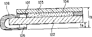
The liquid crystal indicator of recording and narrating in above-mentioned communique as shown in figure 12, is keeping liquid crystal layer 104 between the transparent insulation substrate 102 of portion of external circuit 101 formation and the transparent insulation substrate that disposes relatively therewith (substrate relatively) 103.What this device adopted is to constitute external circuit by semi-conductor chip, be about to IC chip 105 be installed in 101 opposed of transparent insulation substrate 102 external circuits on, and use flexible cable 106 and external circuit 101 to carry out electric being connected.
From Figure 12 obviously as can be known, have the integral thickness tb of the liquid crystal indicator of this composition, have more the thickness t a (for example, 1 millimeter) of IC chip 105 and flexible cable 106 sums.Therefore, liquid crystal indicator is used for the thickness of device of display part also with regard to thickening.Mobile terminal device particularly, pocket telephone for example, the slimming of claimed apparatus own if it is blocked up to be used for the thickness t b of liquid crystal indicator of pocket telephone display part, will hinder the slimming of telephone set itself.
Summary of the invention
The present invention proposes according to above-mentioned technical background and demand, and its objective is provides the slimming that makes whole device to become possible display device, and utilizes the portable terminal of this display device.
Display device of the present invention possesses: formed that a plurality of pixels are the pixel portions of rectangular arrangement and be the 1st substrate that writes the drive system that picture element signal drives to this pixel portions; The 2nd substrate that the 1st substrate is kept predetermined distance and relative configuration; Remain on the material layer with electric optical effect between the 1st and the 2nd substrate, it has the control system of control-driven system, and this control system is a semi-conductor chip, forms on the 1st substrate.This display device is used for the display part of portable terminals such as pocket telephone.
Display device of the present invention and use the mobile terminal device of this display device, because on the substrate that forms drive system, form the control system of controlling this drive system with semi-conductor chip, so the integral thickness of display device does not rely on the thickness of semi-conductor chip.Therefore, can realize the slimming of display device integral body, and then realize using of the slimming of this device as the portable terminal of display part.
The present invention also comprises:
A kind of display device possesses and has formed that a plurality of pixels are the pixel portions of rectangular arrangement and be the 1st substrate that writes the drive system that picture element signal drives to this pixel portions; The 2nd substrate that above-mentioned the 1st substrate is kept predetermined distance and relative configuration; Remain on the material layer between above-mentioned the 1st substrate and above-mentioned the 2nd substrate, it is characterized in that with electric optical effect:
Have the control system of the above-mentioned drive system of control, this control system is a semi-conductor chip, on above-mentioned the 1st substrate, form,
Above-mentioned semi-conductor chip and above-mentioned drive system form at grade,
As the thickness of the above-mentioned semi-conductor chip of above-mentioned control system, be lower than the parts between above-mentioned the 1st substrate of sealing and above-mentioned the 2nd substrate and the thickness sum of above-mentioned the 2nd substrate.
A kind of mobile terminal device is characterized in that:
Utilize a kind of display device as display part, this display device possesses and has formed that a plurality of pixels are the pixel portions of rectangular arrangement and be the 1st substrate that writes the drive system that picture element signal drives to this pixel portions; The 2nd substrate that above-mentioned the 1st substrate is kept predetermined distance and relative configuration; Remain on the material layer between above-mentioned the 1st substrate and above-mentioned the 2nd substrate, wherein with electric optical effect
The control system of controlling above-mentioned drive system is a semi-conductor chip, on above-mentioned the 1st substrate, forms,
Above-mentioned semi-conductor chip and above-mentioned drive system are formed on the same plane,
As the thickness of the above-mentioned semi-conductor chip of above-mentioned control system, be lower than the parts between above-mentioned the 1st substrate of sealing and above-mentioned the 2nd substrate and the thickness sum of above-mentioned the 2nd substrate.
Other purposes of the present invention, by the resulting concrete benefit of the present invention, can be further clear and definite from the embodiment that the following describes explanation.
Description of drawings
Fig. 1 is the frame circuit diagram of expression liquid crystal indicator example of the present invention.
Fig. 2 is the frame circuit diagram of the vertical driver example in the active array type LCD of expression simulation points order type of drive.
Fig. 3 is the frame circuit diagram of the horizontal driver configuration example in the active array type LCD of expression simulation points order type of drive.
Fig. 4 A, Fig. 4 B are the sectional drawings of expression multi-crystal TFT cross-section structure, and Fig. 4 A represents the situation of bottom grid structure, and Fig. 4 B represents the situation of top-gate structure.
Fig. 5 is the cross-sectional view of expression liquid crystal indicator of the present invention.
Fig. 6 is the sectional drawing of the electrical connections structure of expression on-chip circuit part of transparent insulation and IC chip.
Fig. 7 is the block scheme that the active array type LCD of time-division type of drive of the present invention has been used in expression.
Fig. 8 is the frame circuit diagram of horizontal driver example in the active array type LCD of expression time-division type of drive.
Fig. 9 is the circuit diagram of expression time-division switching portion example.
Figure 10 is the frame circuit diagram that other example of the present invention has been used in expression.
Figure 11 is the side view of expression pocket telephone outward appearance of the present invention.
Figure 12 is the cross-sectional view of the existing liquid crystal indicator of expression.
Embodiment
Explain liquid crystal indicator of the present invention and the mobile terminal device that uses this device below with reference to figure.
At first enumerating the example that the present invention is used for the active array type LCD of simulation points order type of drive describes.As shown in Figure 1, the structure that this liquid crystal indicator has is: a plurality of pixels 11 are arranged in the pixel portions (effective pixel area) 12 that matrix form forms, select the vertical driver 13 of each pixel 11 of pixel portions 12 with the behavior unit sequence, the control system 15 that picture element signal is write the horizontal driver 14 of each pixel 11 of selecting with behavior unit and control these drivers 13,14 is installed on the LCD panel 16.
The structure that LCD panel 16 has is: two transparent insulation substrates are arranged (for example, glass substrate) with the relative liquid crystal layer between the substrate of configuration of predetermined distance, in the pixel portions 12, the capable gate line of m (vertical selection wire) 17-1~17-m and n column signal line (source line) 18-1~18-n are routed to matrix form on substrate therein.Pixel 11 is configured in each cross section of gate line 17-1~17-m and signal wire 18-1~18-n.
Each pixel 11 is made up of following part: as the multi-crystal TFT 19 of pixel transistor, its gate electrode is connected with gate line 17-1~17-m, and the source electrode is connected with signal wire 18-1~18-n; Liquid crystal cell (liquid crystal capacitance) 20, its pixel electrode is connected with the drain electrode of this TFT 19; Auxiliary capacitor 21, one of its electrode is connected with the drain electrode of TFT 19.
In this dot structure, liquid crystal cell 20 plays electric capacity.This electric capacity results between pixel electrode and the comparative electrode to this formation that TFT19 forms.Another electrode of the comparative electrode of this liquid crystal cell 20 and auxiliary capacitor 21 is connected in bridging line 22 jointly.As common voltage VCOM, bridging line 22 is supplied with the DC voltage of regulation.
Here, as the method that drives liquid crystal cell 20, used the so-called common reverse that common voltage VCOM is reversed by 1 horizontal period (1H) to drive method.By using this common reverse to drive method, because the polarity of every 1H counter-rotating common voltage VCOM, think can reduce the power supply voltage that picture element signal writes the horizontal driver 14 of each pixel 11, thereby helps to reduce the power consumption of whole device.
As shown in Figure 2, vertical driver 13 is by shift register 31, and level shifter 32 and grid impact damper 33 are formed.When vertical enabling pulse VST input, shift register 31 with the synchronous mode of vertical clock (clock) VCK, sequential delivery this vertical enabling pulse VST, thus export from respectively passing on the level order as shift pulse.
As shown in Figure 3, horizontal driver 14 is by shift register 34, level shifter 35, and data latches circuit 36, D/A converter 37 and impact damper 38 are formed.When horizontal enabling pulse HST input, shift register 34 with the synchronous mode of horizontal clock HCK, the horizontal enabling pulse HST of sequential delivery as exporting in proper order from respectively passing on the shift pulse of level, and carries out horizontal scanning.
In addition, as shown in Figure 1, the control system 15 of control vertical driver 13 and horizontal driver 14, by timing controller (timing controller, TC) 23, reference voltage generates compositions such as source 24 and DC-DC converter 25.These circuit and pixel portions 12 are installed on the same substrate, and vertical driver 13 and horizontal driver 14 promptly are installed on LCD panel 16.
In this control system 15, for example, supply voltage VDD from external power source portion (not having diagram), Digital Image Data data from outer CPU (not having diagram), clock CLK from external clock generator (not having diagram) is input in the timing controller 23 by not shown TCP (tape carrierpackage) respectively.
In addition, in this example, though the storer of CPU, storing image data or clock generator are arranged on the outside of LCD panel 16,, wherein have a part at least as control system 15, can be installed on the LCD panel 16.
Timing controller 23 is carrying out the time-controlled while, respectively vertical enabling pulse VST, vertical clock VCK isochronon signal and various control signal are supplied with vertical driver 13, with horizontal enabling pulse HST, horizontal clock HCK isochronon signal, various control signal and Digital Image Data data supply level driver 14.
Reference voltage generates source 24, produces a plurality of reference voltages with different magnitude of voltage, and with the reference voltage selection type D/A converter 37 of these reference voltage supply level drivers 14 as its reference voltage.DC-DC converter 25 converts the DC voltage (low-voltage) of low-voltage to two or more High Level DC Voltage (high voltage), and it is supplied with vertical driver 13, and horizontal driver 14 and reference voltage generate source 24 and wait each loop.
In the active array type LCD of above-mentioned simulation points order type of drive, the transistor that constitutes vertical driver 13 and horizontal driver 14 is TFT, especially, is the multi-crystal TFT identical with the pixel transistor of pixel portions 12.It is formed on the transparent insulation substrate identical with pixel portions 12, and in the zone of liquid crystal layer with the encapsulant sealing.In this situation, because the polysilicon mobility, the actuating range of the driving frequency of vertical driver 13 and horizontal driver 14 (movement range) is limited at below the 10MHz.
As the pixel transistor of pixel portions 12 and form the transistor of drive system and in the multi-crystal TFT that uses, following two kinds of structures are arranged: gate electrode is configured in bottom grid (bottom gate) structure under the oxide film and gate electrode and is configured in top-gate (topgate) structure on the oxide film.The cross-sectional configuration of these multi-crystal TFTs is shown in Fig. 4 A and Fig. 4 B.
In the bottom grid structure TFT shown in Fig. 4 A, gate electrode 42 is formed on the glass substrate 41, and grid oxidation film 43 is arranged on gate electrode 42, is polysilicon layer 44 then, up is interlayer dielectric 45 again.In addition, on the gate insulating film 43 of gate electrode 42 sides, formed by N
+Source region 46 and drain region 47 that diffusion layer constitutes.Source region 46 is connected with drain electrode 49 with source electrode 48 respectively with drain region 47.
In the top-gate structure TFT shown in Fig. 4 B, polysilicon layer 52 is formed on the glass substrate 51, and grid oxidation film 53 is arranged on polysilicon layer 52, is gate electrode 54 then, up is interlayer dielectric 55 again.In addition, on the glass substrate 51 of polysilicon layer 52 sides, formed by N
+Source region 56 and drain region 57 that diffusion layer constitutes.Source region 56 is connected with drain electrode 59 with source electrode 58 respectively with drain region 57.
On the other hand, the timing controller 23 of control system 15, reference voltage generation source 24 and DC-DC converter 25 are integrated by monocrystalline silicon.Use COG (chip on glass) method that this silicon IC is installed on the plane identical with vertical driver 13 and horizontal driver 14, promptly on the substrate (transparent insulation substrate) that vertical driver 13 and horizontal driver 14 form.The silicon IC that is formed by monocrystalline silicon can turn round at 100MHz.
As mentioned above, because multi-crystal TFT is used for constituting the driven at low speed and the significant circuit part of dispersing characteristic of vertical driver 13 and horizontal driver 14, and use the circuit part of multi-crystal TFT to be sealed in the enclosure space of pixel portions 12.Therefore, can prevent because Na
+Ion is sneaked into and the displacement of the TFT threshold voltage that causes, thereby improves reliability.At this moment, aspect the thickness of liquid crystal indicator, because TFT and liquid crystal cell (liquid crystal layer) thin in comparison get and can ignore, therefore, TFT can not become the reason that liquid crystal indicator self thickness is increased.
On the other hand, the circuit part that the circuit part of high-speed driving or dispersing characteristic are little, promptly timing controller 23, the reference voltage for control system 15 generates source 24 and DC-DC converter 25, it is integrated to carry out monocrystalline silicon, and is installed on the substrate identical with vertical driver 13 and horizontal driver 14.At this moment, the transversal section of liquid crystal indicator as shown in Figure 5.
In Fig. 5, as mentioned above, liquid crystal indicator comprises as the lower part: form the transparent insulation substrate 61 of vertical driver 13 grades, the transparent insulation substrate of relative configuration with it (substrate relatively) 62, and the liquid crystal layer 63 that remains between 61 and 62 and use encapsulant 64 to seal.In this liquid crystal indicator, use the COG method to be installed on the transparent insulation substrate 61 that has formed vertical driver 13 grades the control system 15 integrated IC chips that form 65.
Fig. 6 represents, the structure of electrical connections between circuit part on the transparent insulation substrate 61 and the IC chip 65.In Fig. 6, the circuit part 652 of IC chip 65 is formed on the silicon chip 651, and circuit part 652 is electrically connected with external cabling gangster (padded coaming) 653.This external cabling gangster son 653 is by the circuit layout on anisotropic conductive film 66 and the transparent insulation substrate 61, and for example, aluminum wiring 611 is electrically connected.And, between transparent insulation substrate 61 and IC chip 65, there is interlayer dielectric 67.
Like this, when being installed in IC chip 65 on the transparent insulation substrate 61, with regard to the IC chip itself, during owing to making, formed protective seam on silicon IC, its reliability is out of question.In addition, owing to be the COG structure, metal material partly is necessary to improve reliability to being connected with transparent insulation substrate 61.For this reason, after forming the IC chip on the transparent insulation substrate 61, make a silicones protective seam that covers IC chip 65 and transparent insulation substrate 61.
In above-mentioned mounting structure, the thickness t 1 of IC chip 65 (about 0.7 millimeter) is less than the transparent insulation substrate 62 on opposite and the thickness t 2 of encapsulant 64 sums.Therefore, because the thickness t 3 of liquid crystal indicator integral body does not rely on the thickness t 1 of IC chip 65, so might make the liquid crystal indicator slimming.The thickness sum t3 that is transparent insulation substrate 61, transparent insulation substrate 62 and encapsulant 64 is the thickness of liquid crystal indicator itself.
In addition, because external circuit is integrated, and the IC chip is installed on the transparent insulation substrate 61, so the part that is electrically connected with the external circuit of LCD panel 16 can reduce.Therefore, might improve the reliability of 16 pairs of mechanical vibration of LCD panel etc., and reduce the loose contact that in manufacture process, produces.
In installation component, the physical strength of the IC chip of installing with the COG method 65 is lower than the bond strength of the liquid crystal cell part that forms pixel portions 12 easily.In order to address this problem, the thickness t that the thickness t 1 of IC chip 65 is set in transparent insulation substrate 62 and encapsulant 64 sums preferably is set in the scope thinner than t2 below 2, and such structure makes and is difficult to 65 reinforcings of IC chip from the outside.
In addition, in liquid crystal indicator of the present invention, except making the slimming of device own, in order to make the lightweight of device own, as the substrate material of transparent insulation substrate 61 and 62, PET (polyethylene telephtalete) or PES organic materials such as (polyethersulfone) have been used.
Combination as the substrate material of transparent insulation substrate 61 and 62 has following 4 kinds of situations.Situation 1 is with the substrate material of Si oxide as transparent insulation substrate 61 and 62.Situation 2 is with the substrate material of Si oxide as transparent insulation substrate 61, with the substrate material of organic materials such as PET or PES as transparent insulation substrate 62.Situation 3 is with the substrate material of organic materials such as PET or PES as transparent insulation substrate 61 and 62.Situation 4 is with the substrate material of organic materials such as PET or PES as transparent insulation substrate 61, with the substrate material of Si oxide as transparent insulation substrate 62.
In the substrate material combination of situation 1~situation 4, the combination of situation 3, be about to the substrate material of organic materials such as PET or PES as transparent insulation substrate 61 and 62, because it is corresponding material weight is very light, the most effective for the slimming and the lightweight of liquid crystal indicator itself.
Although above-mentioned example is that the active array type LCD that the present invention is used for simulation points order type of drive is described,, the present invention not only is confined to this.As described below, the present invention is equally applicable to the active array type LCD of so-called time-division type of drive (selective switchgear system).
Fig. 7 is the synoptic diagram that the active array type LCD formation example of time-division type of drive of the present invention has been used in expression.
As shown in Figure 7, being constructed as follows of the active array type LCD of time-division type of drive: be arranged in the pixel portions 72 that matrix form forms by a plurality of pixels 71, select the vertical driver 73 of each pixel 71 of pixel portions 72 with the behavior unit sequence, picture element signal is write the horizontal driver 74 of each pixel 71 of selecting with behavior unit, the time-division switching portion 75 that is used for the time-division, control vertical driver 73, the control system 76 of horizontal driver 74 or time-division switching portion 75, and pixel portions 72 is installed, vertical driver 73, horizontal driver 74, the LCD panel 77 of time-division switching portion 75 and control system 76.
Each pixel 71 is made up of following each several part: gate electrode is connected with each bar gate line 78-1~78-m, and the multi-crystal TFT 80 that source current is connected with each signal line 79-1~79-n, the auxiliary capacitor 82 that 81, one electrodes of the liquid crystal cell that pixel electrode is connected with the drain electrode of TFT80 are connected with the drain electrode of TFT80.In each pixel 71, another electrode of the comparative electrode of liquid crystal cell 81 and auxiliary capacitor 82 is connected in bridging line 83 jointly.As common voltage VCOM, bridging line 83 is supplied with the DC voltage of regulation.
Explained later time-division driving method.So-called time-division driving method is, many signal line that pixel portions 72 is contiguous mutually are divided into 1 unit (piece, block), the signal voltage of many signal line in 1 block will be supplied with, export from the terminal of respectively exporting of horizontal driver 74 in chronological order, be provided with simultaneously the time-division switching portion 75 of many signal line as 1 unit, time-division switching portion 75 will sample by the time-division from the time series signal voltage of horizontal driver 74 outputs, and order offers the driving method of many signal line.
In order to realize the time-division driving, horizontal driver 74 is 1 unit with many signal line, and signal voltage is exported to these signal wires in chronological order.Fig. 8 represents a configuration example of horizontal driver 74.
As shown in Figure 8, horizontal driver 74 is made up of following each several part: shift register 84, one groups of sampling switches 85, level shifter 86, data latches circuit 87 and D/A converter 88.In this example, horizontal driver 74 adopts 5 bit digital view data data, 1~data 5, and supply voltage Vdd and Vss are from the both sides of the sense of displacement of shift register 84.
In horizontal driver shown in Figure 8 74, when horizontal enabling pulse HST input, shift register 84 with the synchronous mode of horizontal clock HCK, the horizontal enabling pulse HST of sequential delivery, as exporting in proper order, and carry out horizontal scanning from respectively passing on the shift pulse of level.Each sampling switch in the sampling switch group 85, response is from the shift pulse (sampling pulse) of shift register 84 order outputs, Digital Image Data data 1~data 5 that sequence checking is imported.
For example, level shifter 86 boosts the 5V numerical data of sampling switch group 85 checks and is the numerical data of liquid crystal drive voltage.Data latches circuit 87 is storeies, and it is stored in the numerical data of the 1H that level shifter 86 boosts.D/A converter 88 adopts reference voltage selection type structures, and it will be exported after will converting analog picture signal to from the Digital Image Data of the 1H of data latches circuit 87 outputs.
As horizontal driver 74, use so-called stringer inversion driving mode.In order to realize the stringer inversion driving, horizontal driver 74 output dependences are odd number or even number and the signal voltage that carries out the current potential counter-rotating in each output terminal, and at each section the polarity of signal voltage are reversed.The stringer inversion driving mode is a kind of, has identical polarity in vertical direction between neighbor, and the type of drive that the polarization state of pixel is reversed on each section.Notice that horizontal driver 74 also can corresponding 1H shared (VCOM) inversion driving.
On the other hand, time-division switching portion 75 is made of analog switch (transmitting switch), and it will be sampled by the time-division from the time series signal voltage of horizontal driver 74 outputs.The concrete configuration example of time-division switching portion 75, as shown in Figure 9.Notice that time-division switching portion 75 is that each output to horizontal driver 74 is provided with.In this example, carry out the driving of 3 time-divisions corresponding to R (red), G (green), B (indigo plant).
Analog switch 75-1, the 75-2 of the CMOS structure that time-division switching portion 75 is formed in parallel by PchMOS transistor and NchNOS transistor and 75-3 form.In this example, as analog switch 75-1,75-2 and 75-3,, also can use the switch of PMOS or NMOS structure though used the switch of CMOS structure.
In time-division switching portion 75, the terminal of respectively importing of 3 analog switch 75-1,75-2 and 75-3 is connected jointly, and each is exported terminal and is connected with each end of 3 signal line 79-1,79-2 and 79-3 respectively.And, to analog switch 75-1,75-2 and 75-3 respectively import terminal, supply with the signal potential of time series mode from horizontal driver 74 outputs.
In addition, disposing and amounting to 6 control line 89-1~89-6, on average each analog switch is 2.And, 2 control input ends of analog switch 75-1, be that transistorized each grid of CMOS is connected in control line 89-1 and 89-2, two control input ends of analog switch 75-2 are connected in control line 89-3 and 89-4, and two control input ends of analog switch 75-3 are connected in control line 89-5 and 89-6.
For 6 control line 89-1~89-6, be 3 analog switch 75-1 of select progressively, 75-2, the grid of 75-3 is selected signal S1~S3, and XS1~XS3 is provided by following timing controller 90 (referring to Fig. 7).Wherein, grid selection signal XS1-XS3 is the reverse signal that grid is selected signal S1~S3.
Grid selects signal S1~S3 and XS1~XS3 to connect in turn 3 analog switch 75-1,75-2 and 75-3, makes with the time series signal voltage of horizontal driver 74 outputs synchronous.Therefore, analog switch 75-1,75-2 and 75-3 sample the time series signal voltage of horizontal driver 74 outputs by the mode of 3 time-divisions during the 1H, supply with corresponding signal lines 79-1,79-2 and 79-3 respectively.
In addition, in Fig. 7, the control system 76 of control vertical driver 73, horizontal driver 74 and time-division switching portion 75, comprise that timing controller 90, reference voltage generate source 91 and DC-DC converter 92 etc., these circuit and pixel portions 72 are installed on the same substrate, and vertical driver 73, horizontal driver 74 and time-division switching portion 75 promptly are installed on LCD panel 77.
In this control system 76, for example, from the supply voltage VDD of external power source portion (not having diagram), from the Digital Image Data data of outer CPU (not having diagram), from the clock CLK of external clock generator (not having diagram), be input in the timing controller 90 by TCP (not having diagram) respectively.
In addition, in this example, though the storer of CPU, storing image data or clock generator are arranged on the outside of LCD panel 77, but, can be with at least one part wherein as control system 76, by control system 76 being integrated into monocrystalline silicon IC (COG), be installed on the LCD panel 77.
And, except that CPU, storer or clock generator, at least one in the various control circuits, such as, the control circuit for light source that is used for LCD, LCD (or EL) show uses graphics controller, further, radio communication line, battery control circuit etc., when using display device of the present invention as the display part of aftermentioned pocket telephone, can be with its part as control system 76, be integrated into monocrystalline silicon IC, and be installed on the LCD panel 77.
Here, the control circuit for light source that is used for LCD is the circuit of backlight or the anterior illumination of control LCD, and the light source (light emitting diode, phosphor-coated light emitting diode) when not giving the pocket telephone standby provides power supply.But, have the function that power supply is provided for the input operation of pocket telephone.Be used for graphics controller that LCD (or EL) shows and be the view data that radio communication line provides is converted to the circuit of the image format that can show, for example, convert the display format of level 160 pixels * vertical 160 pixels at LCD or EL image-region.
Radio communication line is the circuit that is used to communicate by letter, and its receives digital signal or the simulating signal that transmits with the electromagnetic wave form, and converts them to as electric signal digital signal or simulating signal output.When not using, battery control circuit automatically makes the clock low-speed running of CPU, LCD (or EL) panel and graphics controller to reduce power consumption through the regular hour.Simultaneously, when this display device during as the display part of pocket telephone, CPU also has the function that input information when pocket telephone carried out push-botton operation converts numerical data to.
Timing controller 90 is carrying out the time-controlled while, respectively vertical enabling pulse VST, vertical clock VCK isochronon signal and various control signal are supplied with vertical driver 73, with horizontal enabling pulse HST, horizontal clock HCK isochronon signal, various control signal and Digital Image Data data supply level driver 74, and with aforementioned grid selection signal S1~S3, XS1~XS3 supplies with time-division switching portion 75.
Reference voltage generates source 91, produces a plurality of reference voltages with different magnitude of voltage, and with the reference voltage selection type D/A converter 87 of these reference voltage supply level drivers 74 as its reference voltage.DC-DC converter 92 converts the DC voltage (low-voltage) of low-voltage to two or more High Level DC Voltage (high voltage), and it is supplied with each loop such as vertical driver 73, horizontal driver 74 and reference voltage generation source 91.
In the active array type LCD of the time-division of said structure type of drive, constitute the transistor of vertical driver 73 and horizontal driver 74, and each analog switch of forming time-division switching portion 75 is TFT, especially, is the multi-crystal TFT identical with the pixel transistor of pixel portions 72.It is formed on the transparent insulation substrate identical with pixel portions 72, and in the zone of liquid crystal layer with the encapsulant sealing.
On the other hand, the timing controller 90 of control system 76, reference voltage generation source 91 and DC-DC converter 92 usefulness monocrystalline silicon are integrated.Silicon IC is installed on the plane identical with vertical driver 73 and horizontal driver 74 with the COG method, promptly forms on the substrate of vertical driver 73 and horizontal driver 74.
As mentioned above, multi-crystal TFT is used for constituting vertical driver 73, the significant circuit part of the driven at low speed of horizontal driver 74 and time-division switching portion 75 and dispersing characteristic, and the little circuit part of the circuit part of high-speed driving or dispersing characteristic, promptly for the timing controller 90 of control system 76, reference voltage generates source 91 and DC-DC converter 92, because it is integrated to have carried out monocrystalline silicon, and be installed on the substrate identical with vertical driver 73 and horizontal driver 74, therefore, can obtain the identical action effect of active array type LCD with aforementioned simulation points order type of drive.
In this example, though timing controller 90, reference voltage generate source 91 and DC-DC converter 92 is installed in vertical driver 72 1 sides, but, as shown in figure 10, also timing controller 90, reference voltage can be generated source 91 and DC-DC converter 92 and carry out monocrystalline silicon IC (COG) for one, and IC98 is installed on the LCD panel 77 with horizontal driver 73 collection.
Like this, vertical driver 72 1 sides, generate surface area that source 91 and DC-DC converter 92 occupy by timing controller 90, reference voltage and become and do not needed, therefore, LCD panel 77 frame width in the horizontal direction can reduce corresponding footprint area.When therefore, this configuration being used to wish to reduce the display device of horizontal direction frame width also is useful.
In this situation, except that timing controller 90, reference voltage generate source 91 and the DC-DC converter 92, as mentioned above, clearly, also CPU, storer or clock generator further, will be able to be used for the control circuit for light source of LCD, be used for the graphics controller that LCD (or EL) shows, at least one that is used for various control circuits such as the radio communication line of phone and battery control circuit and horizontal driver 73 collect for one and carry out monocrystalline silicon ICization.
In addition, though above-mentioned each object lesson is the material that applies the present invention to have electric optical effect a---liquid crystal, and describe as example with the active array type LCD that uses liquid crystal.But the present invention is equally applicable to use other active matrix type display such as electroluminescent EL display device.
In addition, display device of the present invention, except the display that is used for OA equipment such as PC, word processor and television receiver etc., can also be applicable to pocket telephone or palm PC (personal digital assistants, PAD) display part of mobile terminal device such as grade of carrying out the slimming of device own.
Figure 11 is that mobile terminal device of the present invention has been used in expression, as the side view of pocket telephone outward appearance.
As shown in figure 11, used pocket telephone of the present invention and be made up of following each several part: arranged in order microphone portion 94, display part 95, operating portion 96 and loudspeaker portion 97 from top to bottom in the front of crust of the device 93.In the pocket telephone that constitutes like this, for example, display part 95 has used liquid crystal indicator, and this liquid crystal indicator has used above-mentioned according to liquid crystal indicator of the present invention.
Like this, owing in mobile terminal devices such as pocket telephone, used according to liquid crystal indicator of the present invention as display part 95, this liquid crystal indicator can make the slimming of device own.Therefore, the advantage that has the own slimming of device that makes portable terminal.
As mentioned above, display device of the present invention, because by on the substrate that forms drive system, form the control system of this drive system of control with semi-conductor chip, thereby the thickness of display device integral body does not rely on the thickness of semi-conductor chip, therefore, can make the whole slimming of display device, and can make and utilize this device as the mobile terminal device slimming of display part.
Claims (16)
1. display device possesses and has formed that a plurality of pixels are the pixel portions of rectangular arrangement and be the 1st substrate that writes the drive system that picture element signal drives to this pixel portions; The 2nd substrate that above-mentioned the 1st substrate is kept predetermined distance and relative configuration; Remain on the material layer between above-mentioned the 1st substrate and above-mentioned the 2nd substrate, it is characterized in that with electric optical effect:
Have the control system of the above-mentioned drive system of control, this control system is a semi-conductor chip, on above-mentioned the 1st substrate, form,
Above-mentioned semi-conductor chip and above-mentioned drive system are formed on the plane of same above-mentioned the 1st substrate,
As the thickness of the above-mentioned semi-conductor chip of above-mentioned control system, be lower than the parts between above-mentioned the 1st substrate of sealing and above-mentioned the 2nd substrate and the thickness sum of above-mentioned the 2nd substrate.
2. the display device of claim 1 record is characterized in that:
The pixel transistor of above-mentioned pixel portions and the transistor that constitutes above-mentioned drive system are thin film transistor (TFT)s.
3. the display device of claim 2 record is characterized in that:
Above-mentioned thin film transistor (TFT) is made by polysilicon.
4. the display device of claim 2 record is characterized in that:
Above-mentioned thin film transistor (TFT) is sealed between above-mentioned the 1st substrate and above-mentioned the 2nd substrate with the above-mentioned substance layer.
5. the display device of claim 1 record is characterized in that:
Above-mentioned semi-conductor chip is installed with the COG method.
6. the display device of claim 1 record is characterized in that:
At least one side of above-mentioned the 1st substrate and above-mentioned the 2nd substrate is made by silicon oxide layer or organic material.
7. the display device of claim 1 record is characterized in that:
The above-mentioned substance layer is a liquid crystal layer.
8. the display device of claim 1 record is characterized in that:
The above-mentioned substance layer is an electroluminescence layer.
9. mobile terminal device is characterized in that:
Utilize a kind of display device as display part, this display device possesses and has formed that a plurality of pixels are the pixel portions of rectangular arrangement and be the 1st substrate that writes the drive system that picture element signal drives to this pixel portions; The 2nd substrate that above-mentioned the 1st substrate is kept predetermined distance and relative configuration; Remain on the material layer between above-mentioned the 1st substrate and above-mentioned the 2nd substrate, wherein with electric optical effect
The control system of controlling above-mentioned drive system is a semi-conductor chip, on above-mentioned the 1st substrate, forms,
Above-mentioned semi-conductor chip and above-mentioned drive system are formed on the same plane,
As the thickness of the above-mentioned semi-conductor chip of above-mentioned control system, be lower than the parts between above-mentioned the 1st substrate of sealing and above-mentioned the 2nd substrate and the thickness sum of above-mentioned the 2nd substrate.
10. the mobile terminal device of claim 9 record is characterized in that:
The pixel transistor of above-mentioned pixel portions and the transistor that constitutes above-mentioned drive system are thin film transistor (TFT)s.
11. the mobile terminal device of claim 10 record is characterized in that:
Above-mentioned thin film transistor (TFT) is made by polysilicon.
12. the mobile terminal device of claim 9 record is characterized in that:
Above-mentioned thin film transistor (TFT) is sealed between above-mentioned the 1st substrate and above-mentioned the 2nd substrate with the above-mentioned substance layer.
13. the mobile terminal device of claim 9 record is characterized in that:
Above-mentioned semi-conductor chip is installed with the COG method.
14. the mobile terminal device of claim 9 record is characterized in that:
At least one side of above-mentioned the 1st substrate and above-mentioned the 2nd substrate is made by silicon oxide layer or organic material.
15. the mobile terminal device of claim 9 record is characterized in that:
The above-mentioned substance layer is a liquid crystal layer.
16. the mobile terminal device of claim 9 record is characterized in that:
The above-mentioned substance layer is an electroluminescence layer.
Applications Claiming Priority (2)
| Application Number | Priority Date | Filing Date | Title |
|---|---|---|---|
| JP2000171700A JP4649706B2 (en) | 2000-06-08 | 2000-06-08 | Display device and portable terminal using the same |
| JP171700/00 | 2000-06-08 |
Publications (2)
| Publication Number | Publication Date |
|---|---|
| CN1386255A CN1386255A (en) | 2002-12-18 |
| CN1286078C true CN1286078C (en) | 2006-11-22 |
Family
ID=18674218
Family Applications (1)
| Application Number | Title | Priority Date | Filing Date |
|---|---|---|---|
| CNB018022901A Expired - Fee Related CN1286078C (en) | 2000-06-08 | 2001-06-07 | Display and portable terminal using same |
Country Status (8)
| Country | Link |
|---|---|
| US (1) | US7193677B2 (en) |
| EP (1) | EP1248249B1 (en) |
| JP (1) | JP4649706B2 (en) |
| KR (2) | KR100886885B1 (en) |
| CN (1) | CN1286078C (en) |
| NO (1) | NO326236B1 (en) |
| TW (1) | TWI288288B (en) |
| WO (1) | WO2001095298A1 (en) |
Families Citing this family (21)
| Publication number | Priority date | Publication date | Assignee | Title |
|---|---|---|---|---|
| KR20030068415A (en) * | 2002-02-14 | 2003-08-21 | 샤프 가부시키가이샤 | Display device, electronic appliance and camera |
| TW200407834A (en) * | 2002-09-17 | 2004-05-16 | Seiko Epson Corp | Optoelectronic device, manufacturing method of optoelectronic device, and electronic machine |
| US20040125272A1 (en) * | 2002-12-30 | 2004-07-01 | Chung David B. | Flat panel display with polymer memory provided thereon |
| JP2005031661A (en) * | 2003-06-20 | 2005-02-03 | Toshiba Matsushita Display Technology Co Ltd | Display device |
| JP4651926B2 (en) * | 2003-10-03 | 2011-03-16 | 株式会社 日立ディスプレイズ | Image display device |
| US20050083455A1 (en) * | 2003-10-16 | 2005-04-21 | Chung David B. | Spatially integrated display and memory system |
| US7427985B2 (en) * | 2003-10-31 | 2008-09-23 | Au Optronics Corp. | Integrated circuit for driving liquid crystal display device |
| US7830348B2 (en) * | 2003-12-11 | 2010-11-09 | Au Optronics Corporation | Integrated circuit for liquid crystal display device |
| JPWO2006038253A1 (en) * | 2004-09-30 | 2008-05-15 | 富士通株式会社 | Liquid crystal display |
| TWI288850B (en) * | 2005-02-04 | 2007-10-21 | Chi Mei Optoelectronics Corp | Display module and flat panel display device having the same |
| US20060232579A1 (en) * | 2005-04-14 | 2006-10-19 | Himax Technologies, Inc. | WOA panel architecture |
| TWI319553B (en) | 2005-05-13 | 2010-01-11 | Au Optronics Corp | Organic electro-luminescence display |
| EP1770788A3 (en) * | 2005-09-29 | 2011-09-21 | Semiconductor Energy Laboratory Co., Ltd. | Semiconductor device having oxide semiconductor layer and manufacturing method thereof |
| DE102006005677B4 (en) * | 2006-01-30 | 2015-12-31 | E.G.O. Elektro-Gerätebau GmbH | hob |
| JP5057321B2 (en) | 2006-03-14 | 2012-10-24 | 株式会社ジャパンディスプレイウェスト | Manufacturing method of display device |
| JP2009139774A (en) * | 2007-12-10 | 2009-06-25 | Hitachi Displays Ltd | Display device |
| TWI420480B (en) * | 2009-05-19 | 2013-12-21 | Au Optronics Corp | Electro-optical apparatus and display thereof |
| JP5370189B2 (en) * | 2010-02-04 | 2013-12-18 | セイコーエプソン株式会社 | Electro-optical device substrate, electro-optical device, and electronic apparatus |
| JP5664146B2 (en) * | 2010-11-10 | 2015-02-04 | セイコーエプソン株式会社 | Information display terminal |
| KR102197826B1 (en) * | 2014-09-03 | 2021-01-05 | 삼성디스플레이 주식회사 | Display device |
| CN106412379B (en) | 2016-09-20 | 2019-02-15 | 青岛海信电器股份有限公司 | Realize control method, device and the LCD TV of Frequency Synchronization |
Family Cites Families (25)
| Publication number | Priority date | Publication date | Assignee | Title |
|---|---|---|---|---|
| NL7906695A (en) * | 1979-09-07 | 1981-03-10 | Philips Nv | DISPLAY DEVICE. |
| JPS60238817A (en) * | 1984-05-12 | 1985-11-27 | Citizen Watch Co Ltd | Liquid crystal display device |
| US5849601A (en) * | 1990-12-25 | 1998-12-15 | Semiconductor Energy Laboratory Co., Ltd. | Electro-optical device and method for manufacturing the same |
| JP2791422B2 (en) * | 1990-12-25 | 1998-08-27 | 株式会社 半導体エネルギー研究所 | Electro-optical device and manufacturing method thereof |
| JPH07134279A (en) * | 1993-11-12 | 1995-05-23 | Sharp Corp | Active-matrix type liquid crystal display device |
| JPH07209672A (en) * | 1993-12-03 | 1995-08-11 | Semiconductor Energy Lab Co Ltd | Electronic device with light nonemission type display |
| JP3402400B2 (en) * | 1994-04-22 | 2003-05-06 | 株式会社半導体エネルギー研究所 | Manufacturing method of semiconductor integrated circuit |
| JPH0836190A (en) * | 1994-07-21 | 1996-02-06 | Hitachi Ltd | Liquid crystal display device |
| JP3715996B2 (en) * | 1994-07-29 | 2005-11-16 | 株式会社日立製作所 | Liquid crystal display device |
| JP3889066B2 (en) * | 1994-11-05 | 2007-03-07 | 株式会社半導体エネルギー研究所 | Method for manufacturing semiconductor device |
| JP3593198B2 (en) * | 1995-12-20 | 2004-11-24 | 株式会社半導体エネルギー研究所 | Flat panel display device and liquid crystal panel |
| KR100195501B1 (en) * | 1995-11-30 | 1999-06-15 | 김영남 | Data driving device of flat panel display system using latch type transmitter |
| US6040827A (en) * | 1996-07-11 | 2000-03-21 | Hitachi, Ltd. | Driver circuit, driver integrated circuit, and display device and electronic device using the driver circuit and driver integrated circuit |
| JPH10186393A (en) * | 1996-12-19 | 1998-07-14 | Shin Etsu Polymer Co Ltd | Connector for display inspection of liquid crystal display panel, and production therefor |
| JPH1184425A (en) * | 1997-09-05 | 1999-03-26 | Semiconductor Energy Lab Co Ltd | Electro-optic device |
| US6388652B1 (en) * | 1997-08-20 | 2002-05-14 | Semiconductor Energy Laboratory Co., Ltd. | Electrooptical device |
| JPH1185111A (en) * | 1997-09-10 | 1999-03-30 | Sony Corp | Liquid crystal display element |
| US5994174A (en) * | 1997-09-29 | 1999-11-30 | The Regents Of The University Of California | Method of fabrication of display pixels driven by silicon thin film transistors |
| JPH11265155A (en) * | 1998-03-18 | 1999-09-28 | Toshiba Corp | Substrate for plane type display device |
| JPH11281994A (en) * | 1998-03-31 | 1999-10-15 | Advanced Display Inc | Liquid crystal display |
| JPH11326932A (en) * | 1998-05-19 | 1999-11-26 | Fujitsu Ltd | Liquid crystal display device |
| JPH11338432A (en) * | 1998-05-28 | 1999-12-10 | Advanced Display Inc | Liquid crystal driving ic |
| JPH11352516A (en) * | 1998-06-09 | 1999-12-24 | Matsushita Electric Ind Co Ltd | Active matrix type liquid crystal display panel |
| JP3258284B2 (en) * | 1998-11-10 | 2002-02-18 | セイコーインスツルメンツ株式会社 | Semiconductor circuit |
| EP1031873A3 (en) * | 1999-02-23 | 2005-02-23 | Sel Semiconductor Energy Laboratory Co., Ltd. | Semiconductor device and fabrication method thereof |
-
2000
- 2000-06-08 JP JP2000171700A patent/JP4649706B2/en not_active Expired - Fee Related
-
2001
- 2001-06-07 US US10/049,052 patent/US7193677B2/en not_active Expired - Lifetime
- 2001-06-07 CN CNB018022901A patent/CN1286078C/en not_active Expired - Fee Related
- 2001-06-07 TW TW090113833A patent/TWI288288B/en not_active IP Right Cessation
- 2001-06-07 KR KR1020087006567A patent/KR100886885B1/en not_active IP Right Cessation
- 2001-06-07 KR KR1020027001378A patent/KR100882248B1/en not_active IP Right Cessation
- 2001-06-07 WO PCT/JP2001/004815 patent/WO2001095298A1/en active Application Filing
- 2001-06-07 EP EP01936896A patent/EP1248249B1/en not_active Expired - Lifetime
-
2002
- 2002-02-07 NO NO20020608A patent/NO326236B1/en not_active IP Right Cessation
Also Published As
| Publication number | Publication date |
|---|---|
| KR20080037724A (en) | 2008-04-30 |
| NO20020608D0 (en) | 2002-02-07 |
| EP1248249A4 (en) | 2005-06-22 |
| WO2001095298A1 (en) | 2001-12-13 |
| KR100882248B1 (en) | 2009-02-06 |
| EP1248249B1 (en) | 2012-08-15 |
| NO326236B1 (en) | 2008-10-20 |
| JP2001350421A (en) | 2001-12-21 |
| TWI288288B (en) | 2007-10-11 |
| US7193677B2 (en) | 2007-03-20 |
| US20030112403A1 (en) | 2003-06-19 |
| NO20020608L (en) | 2002-02-07 |
| KR20020020802A (en) | 2002-03-15 |
| KR100886885B1 (en) | 2009-03-05 |
| EP1248249A1 (en) | 2002-10-09 |
| JP4649706B2 (en) | 2011-03-16 |
| CN1386255A (en) | 2002-12-18 |
Similar Documents
| Publication | Publication Date | Title |
|---|---|---|
| CN1286078C (en) | Display and portable terminal using same | |
| US20230252945A1 (en) | Display substrate | |
| CN1174280C (en) | Liquid crystal display device and electronic apparatus comprising it | |
| CN1308906C (en) | Liquid crystal display device | |
| CN1284131C (en) | Driving circuit, photoelectric device and driving method | |
| CN1253843C (en) | Electrooptical plate, its driving method and electronic device | |
| CN1664682A (en) | Active matrix display device | |
| CN1345024A (en) | Display and control method thereof | |
| CN1776801A (en) | Driver chip for a display device and display device having the same | |
| CN1559065A (en) | Display drive control system | |
| CN1622183A (en) | Display system and electronic device employing same | |
| CN101055706A (en) | Display apparatus | |
| CN1783702A (en) | Clock generating circuit and a display device having the same | |
| KR20060112969A (en) | Intagrated chips and liquid crystal display device including the same | |
| CN1741119A (en) | Shift resistor circuit and method of operating the same | |
| CN1591103A (en) | Method of driving liquid crystal display device, liquid crystal display device, and portable electronic apparatus | |
| CN1240034C (en) | Active matrix type display device | |
| US9111483B2 (en) | Display device | |
| CN1904704A (en) | Display device | |
| CN1786802A (en) | Electro-optical device and electronic apparatus | |
| CN1855311A (en) | Shift register, display device, and electronic device | |
| CN101042480A (en) | Scanning signal line driving device, liquid crystal display device, and liquid crystal display method | |
| CN1445595A (en) | Liquid crystal display and electronic device using it | |
| CN1369917A (en) | Semiconductor element, circuit lining, photoelectric device and electronic equipment | |
| JP4877413B2 (en) | Display device and portable terminal using the same |
Legal Events
| Date | Code | Title | Description |
|---|---|---|---|
| C06 | Publication | ||
| PB01 | Publication | ||
| C10 | Entry into substantive examination | ||
| SE01 | Entry into force of request for substantive examination | ||
| C14 | Grant of patent or utility model | ||
| GR01 | Patent grant | ||
| ASS | Succession or assignment of patent right |
Owner name: NIPPON DISPLAY CO., LTD. Free format text: FORMER OWNER: SONY CORPORATION Effective date: 20121123 |
|
| C41 | Transfer of patent application or patent right or utility model | ||
| TR01 | Transfer of patent right |
Effective date of registration: 20121123 Address after: Aichi Patentee after: Japan display West Co.,Ltd. Address before: Tokyo, Japan Patentee before: Sony Corp. |
|
| CF01 | Termination of patent right due to non-payment of annual fee | ||
| CF01 | Termination of patent right due to non-payment of annual fee |
Granted publication date: 20061122 Termination date: 20190607 |