CN1262009C - Semiconductor device - Google Patents

Semiconductor device Download PDF

Info

Publication number
CN1262009C
CN1262009C CNB031462588A CN03146258A CN1262009C CN 1262009 C CN1262009 C CN 1262009C CN B031462588 A CNB031462588 A CN B031462588A CN 03146258 A CN03146258 A CN 03146258A CN 1262009 C CN1262009 C CN 1262009C
Authority
CN
China
Prior art keywords
semiconductor chip
high resistance
inductor element
resistance area
semiconductor
Prior art date
Legal status (The legal status is an assumption and is not a legal conclusion. Google has not performed a legal analysis and makes no representation as to the accuracy of the status listed.)
Expired - Fee Related
Application number
CNB031462588A
Other languages
Chinese (zh)
Other versions
CN1485919A (en
Inventor
吉村鉄夫
Current Assignee (The listed assignees may be inaccurate. Google has not performed a legal analysis and makes no representation or warranty as to the accuracy of the list.)
Fujitsu Semiconductor Ltd
Original Assignee
Fujitsu Ltd
Priority date (The priority date is an assumption and is not a legal conclusion. Google has not performed a legal analysis and makes no representation as to the accuracy of the date listed.)
Filing date
Publication date
Application filed by Fujitsu Ltd filed Critical Fujitsu Ltd
Publication of CN1485919A publication Critical patent/CN1485919A/en
Application granted granted Critical
Publication of CN1262009C publication Critical patent/CN1262009C/en
Anticipated expiration legal-status Critical
Expired - Fee Related legal-status Critical Current

Links

Images

Classifications

    • HELECTRICITY
    • H01ELECTRIC ELEMENTS
    • H01LSEMICONDUCTOR DEVICES NOT COVERED BY CLASS H10
    • H01L27/00Devices consisting of a plurality of semiconductor or other solid-state components formed in or on a common substrate
    • H01L27/02Devices consisting of a plurality of semiconductor or other solid-state components formed in or on a common substrate including semiconductor components specially adapted for rectifying, oscillating, amplifying or switching and having potential barriers; including integrated passive circuit elements having potential barriers
    • H01L27/04Devices consisting of a plurality of semiconductor or other solid-state components formed in or on a common substrate including semiconductor components specially adapted for rectifying, oscillating, amplifying or switching and having potential barriers; including integrated passive circuit elements having potential barriers the substrate being a semiconductor body
    • H01L27/10Devices consisting of a plurality of semiconductor or other solid-state components formed in or on a common substrate including semiconductor components specially adapted for rectifying, oscillating, amplifying or switching and having potential barriers; including integrated passive circuit elements having potential barriers the substrate being a semiconductor body including a plurality of individual components in a repetitive configuration
    • HELECTRICITY
    • H01ELECTRIC ELEMENTS
    • H01LSEMICONDUCTOR DEVICES NOT COVERED BY CLASS H10
    • H01L28/00Passive two-terminal components without a potential-jump or surface barrier for integrated circuits; Details thereof; Multistep manufacturing processes therefor
    • H01L28/10Inductors
    • HELECTRICITY
    • H01ELECTRIC ELEMENTS
    • H01LSEMICONDUCTOR DEVICES NOT COVERED BY CLASS H10
    • H01L27/00Devices consisting of a plurality of semiconductor or other solid-state components formed in or on a common substrate
    • H01L27/02Devices consisting of a plurality of semiconductor or other solid-state components formed in or on a common substrate including semiconductor components specially adapted for rectifying, oscillating, amplifying or switching and having potential barriers; including integrated passive circuit elements having potential barriers
    • H01L27/04Devices consisting of a plurality of semiconductor or other solid-state components formed in or on a common substrate including semiconductor components specially adapted for rectifying, oscillating, amplifying or switching and having potential barriers; including integrated passive circuit elements having potential barriers the substrate being a semiconductor body
    • H01L27/06Devices consisting of a plurality of semiconductor or other solid-state components formed in or on a common substrate including semiconductor components specially adapted for rectifying, oscillating, amplifying or switching and having potential barriers; including integrated passive circuit elements having potential barriers the substrate being a semiconductor body including a plurality of individual components in a non-repetitive configuration
    • H01L27/0611Devices consisting of a plurality of semiconductor or other solid-state components formed in or on a common substrate including semiconductor components specially adapted for rectifying, oscillating, amplifying or switching and having potential barriers; including integrated passive circuit elements having potential barriers the substrate being a semiconductor body including a plurality of individual components in a non-repetitive configuration integrated circuits having a two-dimensional layout of components without a common active region
    • H01L27/0617Devices consisting of a plurality of semiconductor or other solid-state components formed in or on a common substrate including semiconductor components specially adapted for rectifying, oscillating, amplifying or switching and having potential barriers; including integrated passive circuit elements having potential barriers the substrate being a semiconductor body including a plurality of individual components in a non-repetitive configuration integrated circuits having a two-dimensional layout of components without a common active region comprising components of the field-effect type
    • HELECTRICITY
    • H01ELECTRIC ELEMENTS
    • H01LSEMICONDUCTOR DEVICES NOT COVERED BY CLASS H10
    • H01L27/00Devices consisting of a plurality of semiconductor or other solid-state components formed in or on a common substrate
    • H01L27/02Devices consisting of a plurality of semiconductor or other solid-state components formed in or on a common substrate including semiconductor components specially adapted for rectifying, oscillating, amplifying or switching and having potential barriers; including integrated passive circuit elements having potential barriers
    • H01L27/04Devices consisting of a plurality of semiconductor or other solid-state components formed in or on a common substrate including semiconductor components specially adapted for rectifying, oscillating, amplifying or switching and having potential barriers; including integrated passive circuit elements having potential barriers the substrate being a semiconductor body
    • H01L27/08Devices consisting of a plurality of semiconductor or other solid-state components formed in or on a common substrate including semiconductor components specially adapted for rectifying, oscillating, amplifying or switching and having potential barriers; including integrated passive circuit elements having potential barriers the substrate being a semiconductor body including only semiconductor components of a single kind

Landscapes

  • Engineering & Computer Science (AREA)
  • Power Engineering (AREA)
  • Computer Hardware Design (AREA)
  • Microelectronics & Electronic Packaging (AREA)
  • Physics & Mathematics (AREA)
  • Condensed Matter Physics & Semiconductors (AREA)
  • General Physics & Mathematics (AREA)
  • Semiconductor Integrated Circuits (AREA)
  • Metal-Oxide And Bipolar Metal-Oxide Semiconductor Integrated Circuits (AREA)
  • Element Separation (AREA)

Abstract

There is provided a semiconductor device able to prevent performance degradation of an inductor element provided thereon. A high resistance region is provided below the inductor element formed on the semiconductor substrate. The high resistance region is formed deeper than the well regions of the p-channel and n-channel MOS transistors, thus preventing induction of an eddy current by the magnetic flux generated from the inductor element.

Description

Semiconductor device
Cross reference to related application
Present patent application is based on the Japanese patent application No.2002-196118 that submits July 4 in 2002, and its full content is contained in this for your guidance.
Technical field
The present invention relates to a kind of semiconductor device, for example be used for cellular phone, PDA (personal digital assistant) from several MHz to the frequency band of several GHz or the like, and the method that is used for producing the semiconductor devices, be particularly related to and comprise that bipolar device, MOS device and other have the semiconductor device of other active members of the such passive device of inductor element, and manufacture method.
Background technology
Usually, by together being installed in, inductor, capacitor or other passive devices and active member form an electronic-circuit device on the electronic circuit board.But, be starved of the size, thickness or the weight that reduce electronic-circuit device, especially true for mobile phone and PDA especially.In order to address that need, people research and develop for the compactedness and the integrated level of further increase electronic-circuit device.As a kind of method that increases packaging density, developed MMIC (monolithic integrated microwave circuit).This MMIC be one by formation integrated in the semiconductor technology high-frequency integrated circuit that obtains of the such active member of transistor and for example resistor and the such passive device of inductor for example.
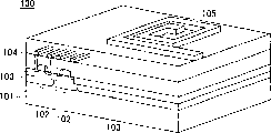
Fig. 1 is the perspective view of cmos device that is formed with the prior art of inductor element.Referring to Fig. 1, cmos device 100 comprise be formed on a semiconductor chip 101 on MOS transistor 102 and element Disengagement zone 103, be formed on this semiconductor chip 101 and be connected to the interconnection structure 104 of MOS transistor 102 and be formed on inductor element 105 on this interconnection structure 104 with the shape of spiral.
By in this manner inductor element being formed on the CMOS, compare with additional external inductance and can obtain higher integrated level, so this being applicable to mobile phone.
Forwarding to will be by problem solved by the invention, and high more then its performance of Q value (quality factor) of well-known inductor element is high more.But if for example electric elements 105 are formed on the cmos device 100, because electric coupling and capacitive coupling between inductor element 105 and the semiconductor chip 101, the Q value of inductor element 105 reduces.For example, as shown in Figure 2, if the resistivity of semiconductor chip 101 is lower, the magnetic field inducing eddy-current in semiconductor chip 101 that is produced by inductor element 105 then.Hindering direction to flow at my electric current, so reducing the Q value by the changes of magnetic field that inductor element produced.
In order to address this problem, to have a kind of method and relate to the resistivity that reduces substrate, to increase the Q value of inductor element.Fig. 3 illustrates the relation between the resistivity of the Q value of inductor element and this substrate.
Referring to Fig. 3, can clearly be seen that the Q value increases when the resistivity of substrate increases.
But, for example in the CMOS manufacturing process, because impurity element is injected into and spreads in semiconductor chip, to form impurity diffusion zone, for example well region; Resistivity in these zones reduces, and easy inducing eddy-current.Hereinafter, as an example, will the manufacturing process of cmos device be described.
Fig. 4 A to 4C illustrates the manufacturing process of cmos device.
In the step shown in Fig. 4 A, by STI, silicon dioxide is embedded in silicon chip 111, and it has for example substrate resistance rate of 1k Ω cm, and forms the element isolation zone 112 of the degree of depth with 300 nanometers, with discrete device district 113A and 113B.
In addition, in the step shown in Fig. 4 A, by photoetching treatment, a device region 113B is covered by photoresist.Inject by ion then, p type dopant ion B +Accelerate to 300keV, and with 1 * 10 13Cm -2Density be injected into other device regions 113A, to form a p well region 114.
Then, remove photoresist, and by use one with the opposite mask of employed mask in above-mentioned lithography step, the device region 113A that covering is used for p well region 114 and other parts is according to identical mode, n type dopant ion P +Inject, to form a n well region 115.Note that an impurity diffusion zone 116 also is formed under the regional 112C that is not capped.
Then, in the step shown in Fig. 4 B, a gate oxidation films 117 is deposited on the thickness that has 2 nanometers on this device region, and a polysilicon membrane is deposited as the thickness with 180 nanometers, forms grid 118 by photoetching treatment then.
In addition, in the step shown in Fig. 4 B, form the silicon dioxide film of 100 nanometer thickness, and carry out corrosion, to form sidewall 119 by RIE (reactive ion etching).Then,, inject dopant ion, to form source region and drain region 120 according to the mode identical with being formed on well region.
Then, in the step shown in Fig. 4 C, form interlayer dielectric 121 and connector 122 and interconnection layer 123.Then, carry out polishing and smooth, to form multilayer interconnect structure by CMP (chemico-mechanical polishing).
In the step shown in Fig. 4 C,, and form spiral helicine inductor element 124 by photoetching and dry etching in addition by on multilayer interconnect structure, carrying out sputter with the film of deposit by 150 made nanometer thickness of aluminium or other metals.In this manner, form the cmos device that has an inductor element in its surface.
As shown in Fig. 4 A, when injecting B +During dopant ion, because just in time the element Disengagement zone 112C below this inductor element 124 is uncovered, and impurity diffusion zone 116 also is formed on the below of this element Disengagement zone 112C.Although the semiconductor chip 111 at native mode has high resistivity, in such impurity diffusion zone, this semiconductor chip 111 becomes conduction.Thereby at this element Disengagement zone 112C, AC (interchange) the magnetic field induction vortex flow that is produced by inductor element 124.When vortex flow flows on the direction of obstruction changes of magnetic field, cause the problems referred to above, promptly the Q value reduces.
Summary of the invention
Correspondingly, general objects of the present invention is the problems referred to above that solve prior art.
A more concrete purpose of the present invention provides a kind of semiconductor device, it can suppress and prevent because the vortex flow that the magnetic field of inductor element is responded to, therefore can prevent the decreased performance of inductor element, and a kind of method that is used to make this semiconductor device is provided.
To achieve these goals, according to first aspect present invention, provide a kind of semiconductor device at this, comprising semiconductor chip, be formed on device region in this semiconductor chip, be formed on impurity diffusion zone in this device region, be formed on an inductor element on the first surface of this semiconductor chip with predetermined substrate resistance rate; And be formed on semiconductor chip that this inductor element is faced mutually in a high resistance area, it has the resistivity higher than the resistivity of this semiconductor chip.
According to foregoing invention, by in the face of in the semiconductor chip of this inductor element, in other words, in these electric elements, form a high resistance area, because the high resistivity of this high resistance area, thereby the magnetic field of the inductor element below this inductor element can inducing eddy-current.
Best, this high resistance area is formed on a position away from impurity diffusion zone with respect to the first surface of this semiconductor chip.
According to foregoing invention, since this high resistance area be formed on respect on the surface of semiconductor chip away from the position of impurity diffusion zone, in other words, be embedded in more in this semiconductor chip with respect to this impurity diffusion zone of surface ratio at semiconductor chip, the impurity diffusion zone wiring layer is not below high resistance area, and the resistivity in this district is higher than the resistivity of impurity diffusion zone.Therefore, even below high resistance area, also be difficult to occur the induction of vortex flow, prevent like this because the decreased performance of the inductor element that the vortex flow induction is caused.
Best, form high resistance area in such a manner, make to be present in described high resistance area and to have between the described semiconductor-based section of substrate resistance rate without any described impurity range.
According to foregoing invention, at this without any the impurity diffusion zone below the high resistance area that is formed in this semiconductor chip.Therefore, in semiconductor chip, be not easy to occur the induction of vortex flow, can prevent like this because the decreased performance of the inductor element that induction caused of vortex flow with resistivity higher than impurity range.
Best, high resistance area comprises groove.Because the groove in high resistance area, even in this region generating vortex flow, this vortex flow is cut apart.
In addition, this high resistance area has a porous part.Because porous material provides the space of complicated shape, should be vortex flow is difficult to form a closure in this material circuit, so the induction of vortex flow be suppressed.
Best, a sunk part is formed on the second surface of the semiconductor chip of facing mutually with described inductor element.
According to foregoing invention, a sunk part is formed on the second surface of the semiconductor chip of facing mutually with described inductor element, for example, and on the rear surface of this semiconductor chip.Therefore, be reduced at the volume of the semiconductor chip that vortex flow induction occurs, thereby suppress vortex flow.Prevent like this because the decreased performance of the inductor element that the vortex flow induction is caused.
To achieve these goals, according to second aspect present invention, provide a kind of method that is used for producing the semiconductor devices at this, comprising following steps: in a semiconductor chip, form a high resistance area, described high resistance area has the resistivity higher than the resistivity of this semiconductor chip, form a transistor in the device region around being formed at this high resistance area, and on this high resistance area, form an inductor element, wherein in forming transistorized step, when being injected into this device region, impurity element covers this high resistance area.
According to foregoing invention, when forming a transistor, this high resistance area is capped, and impurity element is injected into this device region.Therefore, impurity element is injected into high resistance area, and this remains a high resistance area.Therefore, the induction of vortex flow is suppressed.
From hereinafter becoming clearer with reference to these and other purposes of the present invention and advantage the accompanying drawing detailed description of the preferred embodiment.
Description of drawings
Fig. 1 is the perspective view that the existing cmos device that wherein is formed with an inductor element is shown;
Fig. 2 is the schematic diagram that is used to illustrate by an inductor element inducing eddy-current;
Fig. 3 is the schematic diagram that is illustrated in the relation between Q value and the substrate resistance rate;
Fig. 4 A to 4C is the schematic diagram that the technology that is used to make existing C MOS is shown;
Fig. 5 is the perspective view according to the cmos device of first embodiment of the invention;
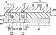
Fig. 6 is the cross sectional view according to the cmos device of first embodiment;
Fig. 7 A to 7D illustrates the schematic diagram (part 1) that is used to make according to the technology of the cmos device of first embodiment;
Fig. 8 E and 8F illustrate the schematic diagram (part 2) that is used to make according to the technology of the cmos device of first embodiment;
Fig. 9 is the cross sectional view according to the cmos device of second embodiment of the invention;
Figure 10 A and 10B illustrate the schematic diagram that is used to make according to the technology of the cmos device of second embodiment;
Figure 11 A and 11B illustrate the schematic diagram that is used to make according to the cmos device of the modification of second embodiment;
Figure 12 is the cross sectional view according to the cmos device of third embodiment of the invention;
Figure 13 A to 13C is the schematic diagram that illustrates owing to making according to the cmos device of the 3rd embodiment;
Figure 14 is the perspective view according to the cmos device of fourth embodiment of the invention;
Figure 15 is the cross sectional view according to the cmos device of fourth embodiment of the invention;
Figure 16 is the flow chart that illustrates according to an example of the method for designing of fifth embodiment of the invention;
Figure 17 A and 17B illustrate the schematic diagram that utilization is handled according to the manufacturing of the method for designing of the 5th embodiment; And
Figure 18 is for illustrating the flow chart according to an example of the method for designing of a modification of fifth embodiment of the invention.
Embodiment
Describe the preferred embodiments of the present invention below with reference to accompanying drawings in detail.
First embodiment
The present invention relates to an example of cmos device, wherein the high resistance area under an inductor element is formed darker than impurity diffusion zone.
Fig. 5 is the perspective view of the cmos device of first embodiment of the invention, and Fig. 6 is its cross sectional view.
Referring to Fig. 5 and Fig. 6, the device region 13A that the device 10 of present embodiment CMOS comprises a semiconductor chip 11, be formed on element Disengagement zone 12 on this semiconductor device substrate 11, separated by element Disengagement zone 12 and 13B, be formed on p raceway groove and n channel MOS transistor 14A and 14B among this device region 13A and the 13B, the connector 16 that is connected to p raceway groove and n channel MOS transistor 14A and 14B and interconnection layer 17, interlayer dielectric 18 and the inductor element 19 that is connected with interconnection layer 17 with connector 16.In addition, the high resistance area under inductor element 19 is formed darker than well region 21A and the 21B of p raceway groove and n channel MOS transistor 14A and 14B.Hereinafter, with the detailed description that provides present embodiment cmos device 10.
Semiconductor chip 11 is formed by the silicon of the resistivity that for example has 1k Ω cm.Viewpoint from the vortex flow that suppresses to be responded to by the magnetic field of inductor element 19 makes that preferably the substrate resistance rate is higher.
P channel MOS transistor 14A comprise by n type diffusion of dopant ions in the semiconductor chip 11 formed n type well region 21A, by the diffusion p formed source region of type dopant ion and drain region 22A and 22B, by at the formed gate insulating film 23 of silicon dioxide film of lip-deep 2 nanometer thickness of this semiconductor chip 11, by formed grid 24 of the polysilicon film of 180 nanometer thickness and side wall insulating film 25.
Inject n type dopant ion, for example P by ion +Ion is accelerated to 600 electron-volts and with 1 * 10 13Cm -2Density be injected into n type well region 21A.The degree of depth of this n trap is about 1000 nanometers with respect to the surface of this semiconductor chip 11 for example.
On the other hand, n channel MOS transistor 14B comprise by diffusion have p type well region 21B that the dopant ion with p channel MOS transistor opposite conductivity type forms, by the diffusion n formed source region of type dopant ion and drain region 22C and 22D, by the formed gate insulating film 23 of the silicon dioxide film of 2 nanometer thickness that on the surface of this semiconductor chip 11, form, by formed grid 24 of the polysilicon film of 180 nanometer thickness and side wall insulating film 25.
Specifically, inject p type dopant ion, for example B by ion +Ion is accelerated to 300keV, and with 1 * 10 13Cm -2Density be injected into p type well region 21B.The degree of depth of p trap is about 1000 nanometers with respect to the surface of this semiconductor chip 11 for example.In addition, because impurity spread, so the resistivity of n trap 21A and p trap 21B becomes tens Ω cm, is lower than the resistivity of semiconductor chip 11.
This interconnection structure comprises by the formed connector 16 of tungsten (W) that connects MOS transistor and their interconnection layer, this interconnection layer 17 is formed by aluminium (Al) or other metal films of about 150 nanometer thickness, and this interlayer dielectric 18 is formed by the silicon dioxide of 300nm.
For example, inductor element 19 is formed on this interconnection structure with spiral-shaped, and its two ends are connected to this interconnection layer 17 by connector 16.
This inductor element 19 is formed by aluminium (Al) or other metal films of 150nm.Specifically, inductor element 19 has 40000 μ m 2To 250000 μ m 2Area, and the thickness of 135 nanometer to 165 nanometers.Note that for inductor element 19, except the helical form inductor element, can also use tortuous inductor or other inductors.
At this semiconductor chip 11 and just below inductor element 19, form high resistance area 20.By the manufacturing step shown in hereinafter, by burying for example such insulating material of silicon dioxide film, silicon oxynitride film and silicon nitride film in the groove that in semiconductor chip 11, forms, and form high resistance area 20.
In addition, high resistance area 20 is formed darker than this element Disengagement zone 12, and darker than the lower end of p trap 21B and n trap 21A.The surface that the degree of depth of high resistance area 20 for example is set to respect to semiconductor chip 11 is 1200 nanometer to 1500 nanometers.That is to say that impurity range is not formed on the below of high resistance area 20.Therefore, the resistivity in the zone below high resistance area 20 is used for the resistivity of this substrate, promptly is higher than the resistivity of p trap 21B and n trap 21A.
By this structure, even when the magnetic flux that electric current produced in inductor element 19 acts on semiconductor chip 11, owing to high resistance area 20 is insulated, so the induction of vortex flow is suppressed.In addition, owing to the zone below high resistance area 20 is the impurity that the part of semiconductor chip 11 does not have diffusion, so the induction of vortex flow is suppressed by high substrate resistance.Thereby, can prevent the decreased performance of inductor element 19.
Then, explanation is used to make the method for the cmos device of present embodiment.
Fig. 7 A to 7D and 8E and 8F illustrate the schematic diagram that is used to make according to the technology of the cmos device of first embodiment.
Referring to Fig. 7 A, handle by photoetching and dry etching, in the silicon chip 11 of the substrate resistance rate that for example has 1k Ω cm, under inductor element 19, as shown in Fig. 5 and Fig. 6, for example, form the dark groove 11-1 of 1000nm.More specifically, the degree of depth of this groove 11-1 be selected such that it with the degree of depth sum that will in next procedure, remove greater than the degree of depth of described n trap 21A and p trap 21B hereinafter.
Then, in the step shown in Fig. 7 B, still by photoetching and dry etching, in a wide region that comprises the groove 11-1 that has formed, for example form a groove 11-3 that 300nm is dark, and be formed for separating the groove 11-2A and the 11-2B of MOS transistor simultaneously.By this step, form the groove 11-3 that 1300nm is dark in this semiconductor chip 11 under this inductor element.
In addition, in the step shown in Fig. 7 B, by CVD (chemical vapor deposition) or the like, silicon dioxide film of deposit is the thickness with 1600nm, and buries this groove 11-2A, 11-2B and 11-3 by this silicon dioxide.
In addition, in the step shown in Fig. 7 B, this silicon dioxide film is polished, be exposed up to semiconductor chip 11 by the CMP method.By above-mentioned steps, form high resistance area 20 and element Disengagement zone 12.
Then, in the step shown in Fig. 7 C,, use p trap mask to carry out composition, 31 cover other substrate surfaces except the zone of the n channel MOS transistor 14B that will be formed with photoresist by photoetching treatment.Inject by ion, B +Dopant ion accelerates to 300keV, and with 1 * 10 13Cm -2Density be injected into this device region 13B, to form p well region 21B.
Specifically, inject by ion, for example B +Dopant ion accelerates to the preset range from 285keV to 315keV, and with respect to the diffusion into the surface of this semiconductor chip 11 to the degree of depth, to form p well region 21B from 700nm to 1000nm.
Then, in the step shown in Fig. 7 D, remove photoresist 31, and, 32 cover the device region that has formed p well region 21B with photoresist by using the n trap mask that p trap mask counter-rotating used in above-mentioned lithography step is obtained.Then, inject by ion, P +Dopant ion accelerates to 600keV, and with 1 * 10 13Cm -2Density be injected into this device region 13B, to form p well region 21A.
Specifically, inject by ion, for example P +Dopant ion accelerates to the preset range from 570keV to 630keV, and with respect to the diffusion into the surface of this semiconductor chip 11 to the degree of depth, to form n well region 21A from 700nm to 1000nm.
In this step, when injecting P +During dopant ion, the photoresist mask is not formed in the high resistance area 20 under this inductor element 19.As a result, dopant ion also is injected into this high resistance area 20.But it is darker that this high resistance area 20 is formed the degree of depth that can arrive than this dopant ion, promptly darker than n trap and p trap, and the result does not have impurity diffusion zone to be formed on the below of this high resistance area 20.
In addition, in the step shown in Fig. 7 D, remove photoresist 32, under 1000 ℃ temperature, carry out annealing, be used for activating.
Then, in the step shown in Fig. 8 E, carry out thermal oxidation by the surface to this semiconductor chip 11, deposit has the thick gate oxidation films of 2nm 23, and on this gate oxidation films 23, forms the thick polysilicon film of 180nm by CVD.Then, after carrying out composition, the use photoetching method forms grid 24 by dry etching.
In addition, in the step shown in Fig. 8 E, cover a device region 13B with mask by photoetching treatment.Inject by ion, BF 2 +Dopant ion accelerates to 10keV, and with 1 * 10 14Cm -2Density be injected into other device regions 13A, to form p type LDD (lightly doped drain) district (not shown).In addition, As +Dopant ion is accelerated to 10keV, and with 1 * 10 14Cm -2Density be injected into other device regions 13A, to form n type LDD district (not shown).
In addition, in the step shown in Fig. 8 E, form the silicon dioxide film that 100nm is thick, and carry out etching, to form sidewall 25 by RIE by the CVD method.Then, according to form the identical mode in LDD zone, form source region and drain region 22A to 22D.
In addition, in the step shown in Fig. 8 E,, under 1000 ℃ temperature, carry out the heat treatment in 3 seconds, be used for activating by RTA (rapid thermal annealing).
Then in the step shown in Fig. 8 F, a silicon dioxide film is deposited on the surface of this substrate by the CVD method.Then smooth by the execution of CVD method, to form interlayer dielectric 18A.Then, leave contact hole, and, carry out polishing by CMP then, in this contact hole, to form connector 16 to a tungsten film deposit by the thickness that the CVD method is 300nm by photoetching and dry etching.
In addition, in the step shown in Fig. 8 F, form the Al film that 150nm is thick, and form this interconnection layer 17 by photoetching and dry etching by sputter.Then, by the silicon dioxide film of a 300nm of CVD formation, and smooth by the CMP execution, to form interlayer dielectric 18B.Then, according to forming interconnection layer 17 and connector 16 with identical mode mentioned above.
In addition, in the step shown in Fig. 8 F, an Al or other metal film depositions are had the thickness of 150nm on this interconnection structure, and form a spiral helicine inductor element 19 by photoetching and dry etching by sputtering method.
In this manner, form the cmos device 10 of present embodiment.
As indicated above, according to present embodiment, it is darker that the high resistance area 20 under this inductor element 19 is formed the lower end that likens to the p trap of impurity range and n trap 21.Because high resistance area 20 is an insulator, it prevents the induction of vortex flow, thereby does not form impurity range below this high resistance area, and high substrate resistance rate prevents the induction of vortex flow.Correspondingly, can avoid the decreased performance of inductor element 19.
Second embodiment
Present embodiment relates to an a kind of example of cmos device, comprising a plurality of grooves cut apart pattern be formed on inductor element under the surface below of high resistance area on.Except pattern was cut apart in formation, present embodiment was identical with first embodiment.
Fig. 9 is according to the cross sectional view of the cmos device of second embodiment of the invention.In Fig. 9, identical reference number is assigned to and identical parts mentioned above, and will omit description of them.
Referring to Fig. 9, the device region 13A that the cmos device 40 of present embodiment comprises semiconductor chip 11, be formed on element Disengagement zone 12 on this semiconductor chip 11, separated by this element Disengagement zone 12 and 13B, be formed on p raceway groove and n channel MOS transistor 14A and 14B among device region 13A and the 13B, the connector 16 that is connected to p raceway groove and n channel MOS transistor 14A and 14B and interconnection layer 17, interlayer dielectric 18 and the inductor element 19 that is connected with connector 16 or interconnection layer 17.In addition, a plurality of groove 41-1 be formed on inductor element 19 under the lower surface of high resistance area 41 on.
The lower surface of the high resistance area 41 under inductor element 19 for example is formed the width (being preferably 1.0 μ m to 2.0 μ m) that has 0.1 μ m to 200 μ m respectively, being spaced apart 0.1 μ m to 50 μ m (being preferably 0.5 μ m to 1.0 μ m) and being 1200nm to 1400nm with respect to the degree of depth on the surface of semiconductor chip 11 between groove, and forms on a direction of the interior surface of this semiconductor chip 11 at least.Identical with first embodiment, in high resistance area 41 and groove 41-1, bury for example such insulating material of silicon dioxide film.
In addition, form impurity diffusion zone 42 in the semiconductor chip between groove 41-1 11.When forming n well region 21A, owing to being injected into, n type dopant ion do not have the photoresist mask to be provided in the high resistance area 41, and this impurity diffusion zone 42 is formed and extends to about and the identical degree of depth of n well region 21A.
By a kind of like this structure, though when the magnetic flux that electric current produced that in inductor element 19, flows almost with semiconductor chip 11 when perpendicular, the induction of vortex flow does not appear in the high resistance area 41, as in first embodiment yet.In the impurity diffusion zone 42 of the high resistance area 41 between groove 41-1, because this resistivity is lower than the resistivity of substrate, therefore, in this inducing eddy-current easily.But owing to the vortex flow of answering by the groove 41-1 segmented sense in high resistance area 41, therefore the vortex flow of induction is suppressed.Thereby, can prevent the decreased performance of inductor element 19.
Then, use description to make a kind of method of the cmos device of present embodiment.
Figure 10 A and 10B illustrate a kind of processing that is used to make according to the cmos device of second embodiment.Hereinafter, the description that repeats mutually with first embodiment will be omitted.
In the step shown in Figure 10 A,, in the silicon chip 11 of the substrate resistance rate that for example has 1k Ω cm, form the dark groove 11-4 of 1000 nanometers by photoetching and dry etching.More specifically, it is dark that for example groove 11-4 is set to 900 nanometer to 1100 nanometers, and 0.1 μ m to 200 μ m (being preferably 1.0 μ m to 2.0 μ m) is wide, and the spacing between this groove is 0.1 μ m to 50 μ m (being preferably 0.5 μ m to 1.0 μ m).This groove 11-4 is formed on this in the silicon chip under the inductor element 19 11.
Then, in the step shown in Figure 10 B, still form the dark groove 11-5 of 300 nanometers by photoetching and dry etching method.The degree of depth that is cut into the groove 11-5 bottom from these semiconductor chip 11 surfaces to groove 41-1 that comprises above-mentioned groove 11-4 is 1200 nanometer to 1400 nanometers.In addition, also be formed for cutting apart the groove 11-2 of MOS transistor.
In addition, in the step shown in Figure 10 B, by CVD or additive method, the silicon dioxide film of deposit 1600 nanometer thickness polishes with smooth by the CMP method then, to form high resistance area 42 and element Disengagement zone 12.
Then, in the step shown in Figure 10 B, as shown in Fig. 7 C and 7D, form p trap and n well region 21.As shown in Fig. 7 D, when forming the n well region, the photoresist mask is not formed in the high resistance area 41, and n type impurity diffusion zone 42 is formed between the groove 41-1 in the high resistance area 41.
Subsequent step is identical with the step shown in the 8F with Fig. 8 E among first embodiment, and forms the cmos device of present embodiment as shown in Figure 9 by these steps.
As indicated above, according to present embodiment, be formed on inductor element 19 under high resistance area 41, on its lower surface, has a plurality of groove 41-1, thereby cut apart inducing eddy-current, and the induction of vortex flow is suppressed.In addition, because at the groove of the bottom of high resistance area, can reduce sinking of the depression that in planarization step process, produced or other parts by the CMP method.
Note that in the present embodiment, as indicated above, when forming n well region 21A, inject n type dopant ion, and in high resistance area 41, do not form the photoresist mask, but shown in the step among Figure 11 A and the 11B, the photoresist mask also is formed in the high resistance area 41.
Figure 11 A and 11B illustrate the schematic diagram that is used to make according to the processing of the cmos device of the modification of second embodiment.
Referring to Figure 11 A,, form a p well region as in the step of Figure 10 of second embodiment B.Specifically, by the device region 13A on the side of photoresist 31 covering n well region 21A and high resistance area 41, and by ion injection, B +Dopant ion is accelerated to 300keV, and with 1 * 10 13Cm -2Density be injected into this device region 13B, to form p well region 21B.
Then, in the step shown in Figure 11 B, remove photoresist 31, and cover the device region 13B on the side of p well region 21B and high resistance area 41 by photoresist 33.Inject by ion, P +Dopant ion accelerates to 600keV, and with 1 * 10 13Cm -2Density be injected into this device region 13A, to form n well region 21A.
In this manner, because dopant ion is not injected into high resistance area 41, so impurity range is not formed in the substrate between the groove 41-1.Correspondingly, this substrate area has the substrate resistance rate and for high resistance state, thereby is not easy to occur the induction of vortex flow, and the induction of vortex flow is suppressed.Therefore, can prevent the decreased performance of inductor element 19.
The 3rd embodiment
Present embodiment relates to an example of cmos device, wherein porous layer be formed on inductor element under high resistance area in.Except forming porous layer, present embodiment and first
Embodiment is identical.
Figure 12 is the cross sectional view according to the cmos device of third embodiment of the invention.In Figure 12, identical reference number represents and components identical mentioned above, and will omit the explanation to them.
Referring to Figure 12, the device region 13A that the cmos device 50 of present embodiment comprises semiconductor chip 11, be formed on element Disengagement zone 12 on the semiconductor chip, separated by this element Disengagement zone 12 and 13B, be formed on p raceway groove and n channel MOS transistor 14A and 14B among device region 13A and the 13B, the connector 16 that is connected to p raceway groove and n channel MOS transistor 14A and 14B and interconnection layer 17, interlayer dielectric 18 and the inductor element 19 that is connected with connector 16 or interconnection layer 17.In addition, porous layer 52 be formed on inductor element 19 under the lower surface of high resistance area 51 on.
Porous layer 52 is to obtain by the silicon of a part of semiconductor chip 11 is converted to porous state.For example, its thickness is set to 900 nanometer to 1100 nanometers.Because porous silicon forms the space of a complicated shape, therefore be difficult in this material, form the vortex flow of closed-loop path, and suppress the induction of vortex flow.Therefore, can prevent the decreased performance of inductor element.
Then, use description to make a kind of method of the cmos device of present embodiment.
Figure 13 A to 13C illustrates the schematic diagram that is used to make according to the processing of the cmos device of the 3rd embodiment.
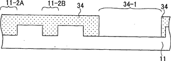
Referring to Figure 13 A, by photoetching and dry etching, in silicon chip 11, form 300 nanometers dark groove 11-2A, 11-2B, 11-6 is the degree of depth of 300nm.Form these grooves for element Disengagement zone 12 and the high resistance area under inductor element 19 51.
Then, in the step shown in Figure 13 B, form photoresist 34, make it have opening corresponding to the position of the groove 11-6 under this inductor element 19 by photoetching method.
Then, in the step shown in Figure 13 C, the porous layer 52 of the middle formation of the perforate 34-1 in semiconductor chip 11.Specifically, for example by anodic oxidation, in HF solution, use Pt as negative electrode, switching current is set to 100mA/cm 2, and switching current greater than 12 minutes is provided in this semiconductor chip 11.As a result, form the porous layer 52 of 1000 nanometer thickness.
In addition, in the step shown in Figure 13 C, by CVD or additive method, the silicon dioxide film of deposit 400 nanometer thickness then, polishes with smooth by CMP, to form high resistance area 51 and element Disengagement zone 12.
As indicated above, according to present embodiment, under the high resistance area under the inductor element 19 51, form a porous layer, and because the shape of this porous layer, make the induction that can occur vortex flow hardly, thereby can suppress the decreased performance of inductor element 19.In addition, the element Disengagement zone under inductor element is formed and the identical degree of depth in element Disengagement zone that is used to separate MOS transistor.Therefore, can reduce undertaken occurring depression or local sinking in the smooth step process by CMP.
The 4th embodiment
Present embodiment relates to an example of cmos device, and wherein the rear surface of the semiconductor chip under inductor element is ground and removed.
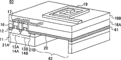
Figure 14 is the cross sectional view according to the cmos device of fourth embodiment of the invention.Figure 15 is its cross sectional view.In Figure 14 and 15, identical reference number represents and components identical mentioned above, and will omit the explanation to them.
Referring to Figure 14 and 15, the device region 13A that the cmos device 60 of present embodiment comprises semiconductor chip 11, be formed on element Disengagement zone 12 on the semiconductor chip 11, separated by this element Disengagement zone 12 and 13B, be formed on p raceway groove and n channel MOS transistor 14A and 14B among device region 13A and the 13B, the connector 16 that is connected to p raceway groove and n channel MOS transistor 14A and 14B and interconnection layer 17, interlayer dielectric 18 and the inductor element 19 that is connected with connector 16 or interconnection layer 17.In addition, only high resistance area 61 is under inductor element 19, an and part of removing this semiconductor chip from this rear surface forms a depression 62.In other words, on rear surface, provide a depression 62, make it have an area that is equal to or greater than by the occupied area of this inductor element 19 corresponding to the semiconductor chip 11 of inductor element 19.
For example, this depression 62 can form in the following manner.
At first, be pre-formed location hole, arrive its rear surface to pass this semiconductor chip 11 from its first type surface.These holes can be used as the reference by location that is used for mask in the process of carrying out photoetching treatment on the rear surface corresponding to the semiconductor chip 11 of this inductor element 19.Note that and to use the bilateral calibrator on the rear surface of this semiconductor chip 11, to carry out composition.
After forming photoresist, use this photoresist as mask, carry out corrosion to form depression 62 by dry etching.
According to present embodiment, have electric current in the inductor element 19 on being formed at this semiconductor chip 11 when flowing, produce magnetic flux, and almost perpendicular with this semiconductor chip 11.But, since only high resistance area 61 be formed on this inductor element under, therefore can prevent the induction of vortex flow.Thereby, can avoid the decreased performance of inductor element 19.
Note that can be before forming element Disengagement zone 12 or after forming inductor element execution to the step of the corrosion of the rear surface of this semiconductor chip 11.In addition, in the present embodiment, it is identical with the degree of depth of the element Disengagement zone 12 that is used to separate MOS transistor that the degree of depth of high resistance area 61 can be set to, but with identical among first embodiment, high resistance area 61 under this inductor element 19 can be formed darker, reduces to be used to form the etching extent of depression 62 like this.
In addition, can provide a plurality of depressions 62.For example, on this rear surface, can on the zone that is equal to or greater than the area occupied, the mode with grid form groove by this inductor element 19.Best, the bottom of each groove arrives high resistance area 61, thereby the vortex flow of this induction is cut apart.
The 5th embodiment
Present embodiment relates to the mask that is used for when the process of making cmos device forms impurity range photoresist being carried out composition.
Figure 16 is the flow chart that illustrates according to an example of the method for designing of fifth embodiment of the invention.Provide description with reference to Figure 16 hereinafter.
At first, from the cmos device circuit design data, produce the pattern (step 201) of the substrate area that comprises device region, element Disengagement zone or the like by well-known method.Then, according to these patterns, produce the mask data (step 202) that is used for only making perforate in the position that forms the p trap.Then, according to these patterns, produce the mask data (step 203) that is used for only making perforate in the position that forms the n trap.By these steps, produce the mask data that is used for p trap and n trap.
Figure 17 A and 17B are illustrated in use and make mask carries out composition afterwards to photoresist by photoetching example by p trap mask data and n trap mask data that said method produced.At this, will be example with the cmos device 40 of second embodiment.
Referring to Figure 17 A, at first use mask by p trap data made, cover this n trap device region 13A and high resistance area 41 with this mask 35.By in the step described in first embodiment, p type impurity element is injected to form a p well region 21B.
Then, in the step shown in Figure 17 B, use mask, cover p trap device region 13B and high resistance area 41 by photoresist 36 by this n trap data made.By identical processing, n type impurity element is injected to form a n well region 21A.
Produce mask data in this manner, therefore impurity element is not injected in the high resistance area 41, impurity element is not infused in semiconductor chip between the high resistance raceway groove, and keeps high substrate resistance rate, thereby occur the induction of vortex flow hardly, and the induction of vortex flow is suppressed.Therefore, can prevent the decreased performance of inductor element 19.
As modification, can design a mask in the following manner to the 5th embodiment.
Figure 18 is another example that illustrates according to a kind of method for designing of present embodiment.Hereinafter, describe with reference to Figure 18.
At first, from the cmos device circuit design data, produce the pattern (step 211) of the substrate area that comprises device region, element Disengagement zone or the like by well-known method.Then, according to these patterns, produce the mask data (step 212) that is used for only making perforate in the position that forms the p trap.
Then, produce the mask data (being called as n trap mask data) (step 213) that is used for making a perforate in other position except the position that forms the p trap is by these data of counter-rotating.Then,, therefore produce inductance component area data (step 214) because high resistance area under inductor element is opened, and append to and with n trap mask data combined (step 215).In this manner, produce p trap mask data and n trap mask data.
Have the effect identical by the mask that uses the data creating that produces in this manner with the 5th embodiment.In addition, when producing mask data in this manner, the amount of inductance component area data is much smaller than the amount of n trap data.And, compare with n trap data conditions with producing p trap data respectively, can reduce to use the design work of CAD or additive method widely.
Although present invention is described with reference to the specific embodiment that is used for illustrative purposes, obviously the invention is not restricted to these embodiment, those of ordinary skill in the art can make various modification and not break away from basic thought of the present invention and scope.
For example, although use cmos device to be described as an example in the above-described embodiments, the present invention can also be applied to BiCMOS device and silicon bipolar device.
Sum up effect of the present invention, be clearly shown that as mentioned, according to the present invention, by than assorted Darker position, matter diffusion district is in the semiconductor chip and forms high resistance area, can suppress Because the magnetic field that the inductor element that provides at semiconductor chip produces causes at high resistance area Inducing eddy-current in the territory. In addition, by in high resistance area, forming groove or porous part, whirlpool Electric current is divided. As a result, can provide that a kind of performance that can prevent inductor element descends half Conductor device.

Claims (9)

1. semiconductor device comprises:
Semiconductor chip with predetermined substrate resistance rate;
Be formed on the device region in this semiconductor chip;
Be formed on the impurity diffusion zone in this device region;
Be formed on the inductor element on the first surface of this semiconductor chip; And
Be formed on semiconductor chip that this inductor element is faced mutually in a high resistance area, it has the resistivity higher than the resistivity of this semiconductor chip,
One of them sunk part is formed on the second surface of the described semiconductor chip of facing mutually with described inductor element.
2. semiconductor device according to claim 1 wherein forms high resistance area in such a manner, makes to be present in described high resistance area and to have between the zone of described semiconductor chip of substrate resistance rate without any impurity range.
3. semiconductor device according to claim 1, wherein said high resistance area are formed on a position more farther than described impurity diffusion zone with respect to the first surface of this semiconductor chip.
4. semiconductor device according to claim 1, wherein said high resistance area comprises groove.
5. semiconductor device according to claim 1, wherein said high resistance area comprise a porous part.
6. semiconductor device according to claim 1, wherein said sunk part is formed such degree of depth with respect to this second surface, promptly makes to form described high resistance area.
7. semiconductor device according to claim 6, wherein said sunk part comprises a plurality of depressions.
8. semiconductor device according to claim 1, wherein said high resistance area is formed by silica.
9. a method that is used for producing the semiconductor devices comprises the steps:
Device region at semiconductor chip forms transistor;
On the first surface of described semiconductor chip, near forming inductor element on the resistance area of described device region;
On the second surface of the semiconductor chip of facing mutually with described inductor element, form sunk part, to prevent the vortex flow of being inducted by the magnetic field of described inductor element, the area of described sunk part is equal to or greater than described inductor element area occupied.
CNB031462588A 2002-07-04 2003-07-04 Semiconductor device Expired - Fee Related CN1262009C (en)

Applications Claiming Priority (2)

Application Number Priority Date Filing Date Title
JP2002196118A JP4355128B2 (en) 2002-07-04 2002-07-04 Semiconductor device and manufacturing method thereof
JP196118/2002 2002-07-04

Publications (2)

Publication Number Publication Date
CN1485919A CN1485919A (en) 2004-03-31
CN1262009C true CN1262009C (en) 2006-06-28

Family

ID=29997038

Family Applications (1)

Application Number Title Priority Date Filing Date
CNB031462588A Expired - Fee Related CN1262009C (en) 2002-07-04 2003-07-04 Semiconductor device

Country Status (5)

Country Link
US (1) US6867475B2 (en)
JP (1) JP4355128B2 (en)
KR (1) KR101005961B1 (en)
CN (1) CN1262009C (en)
TW (1) TWI286819B (en)

Families Citing this family (25)

* Cited by examiner, † Cited by third party
Publication number Priority date Publication date Assignee Title
JP2004214561A (en) * 2003-01-08 2004-07-29 Oki Electric Ind Co Ltd Semiconductor device and method for manufacturing same
JP4651920B2 (en) * 2003-07-15 2011-03-16 ルネサスエレクトロニクス株式会社 Semiconductor device
SE0302107D0 (en) * 2003-07-18 2003-07-18 Infineon Technologies Ag Electromagnetic device and method of operating the same
US7075167B2 (en) * 2003-08-22 2006-07-11 Agere Systems Inc. Spiral inductor formed in a semiconductor substrate
CN1591788A (en) * 2003-08-27 2005-03-09 上海宏力半导体制造有限公司 Method for treating polysilicon
CN1282246C (en) * 2003-09-01 2006-10-25 上海宏力半导体制造有限公司 High-power RF integrated circuit capable of blocking parasitic loss current and its mfg. method
SE526360C2 (en) * 2004-01-09 2005-08-30 Infineon Technologies Ag Monolithic integrated circuit
US20060097346A1 (en) * 2004-11-10 2006-05-11 Advanpack Solutions Pte Ltd Structure for high quality factor inductor operation
US7501690B2 (en) * 2005-05-09 2009-03-10 International Business Machines Corporation Semiconductor ground shield method
JP4661715B2 (en) * 2006-07-21 2011-03-30 セイコーエプソン株式会社 Antenna device
US8860544B2 (en) * 2007-06-26 2014-10-14 Mediatek Inc. Integrated inductor
US7943857B2 (en) * 2008-01-16 2011-05-17 Ralink Technology Corporation Sliced electromagnetic cage for inductors
US8106479B1 (en) * 2008-10-01 2012-01-31 Qualcomm Atheros, Inc. Patterned capacitor ground shield for inductor in an integrated circuit
JP2010118471A (en) * 2008-11-12 2010-05-27 Panasonic Corp Semiconductor device
US7935549B2 (en) * 2008-12-09 2011-05-03 Renesas Electronics Corporation Seminconductor device
US20100295150A1 (en) * 2009-05-22 2010-11-25 Chan Kuei-Ti Semiconductor device with oxide define dummy feature
US8108803B2 (en) * 2009-10-22 2012-01-31 International Business Machines Corporation Geometry based electrical hotspot detection in integrated circuit layouts
CN102820286A (en) * 2012-07-16 2012-12-12 昆山华太电子技术有限公司 Structure for improving performance of passive device of power integrated circuit
US8652934B1 (en) * 2012-12-26 2014-02-18 Micron Technology, Inc. Semiconductor substrate for photonic and electronic structures and method of manufacture
KR102116147B1 (en) * 2014-03-06 2020-05-28 매그나칩 반도체 유한회사 Buried Magnetic Sensor
CN104979200B (en) * 2014-04-03 2018-04-27 中芯国际集成电路制造(上海)有限公司 The forming method of semiconductor devices
CN107658288B (en) * 2014-11-21 2020-02-07 威锋电子股份有限公司 Integrated circuit device
US11139239B2 (en) * 2019-10-01 2021-10-05 Taiwan Semiconductor Manufacturing Company, Ltd. Recessed inductor structure to reduce step height
WO2021081728A1 (en) * 2019-10-29 2021-05-06 华为技术有限公司 Semiconductor device and manufacturing method therefor
FR3142603A1 (en) * 2022-11-28 2024-05-31 Stmicroelectronics (Crolles 2) Sas Integrated circuit comprising a passive component in an interconnection part, corresponding manufacturing process.

Family Cites Families (8)

* Cited by examiner, † Cited by third party
Publication number Priority date Publication date Assignee Title
JPH0677407A (en) * 1992-04-06 1994-03-18 Nippon Precision Circuits Kk Semiconductor device
JPH09270515A (en) * 1996-04-01 1997-10-14 Matsushita Electric Ind Co Ltd Semiconductor device
JP2001168288A (en) * 1999-12-13 2001-06-22 Seiko Epson Corp Semiconductor device
US7575969B2 (en) * 2000-03-02 2009-08-18 Texas Instruments Incorporated Buried layer and method
JP3715502B2 (en) 2000-03-14 2005-11-09 株式会社東芝 Semiconductor device and manufacturing method thereof
JP4776752B2 (en) * 2000-04-19 2011-09-21 ルネサスエレクトロニクス株式会社 Semiconductor device
JP4969715B2 (en) * 2000-06-06 2012-07-04 ルネサスエレクトロニクス株式会社 Semiconductor device
JPWO2002056381A1 (en) * 2001-01-16 2004-05-20 ソニー株式会社 Semiconductor device and manufacturing method thereof

Also Published As

Publication number Publication date
US20040004255A1 (en) 2004-01-08
JP4355128B2 (en) 2009-10-28
JP2004039924A (en) 2004-02-05
KR20040004153A (en) 2004-01-13
US6867475B2 (en) 2005-03-15
CN1485919A (en) 2004-03-31
KR101005961B1 (en) 2011-01-05
TWI286819B (en) 2007-09-11
TW200401407A (en) 2004-01-16

Similar Documents

Publication Publication Date Title
CN1262009C (en) Semiconductor device
CN1251316C (en) Semiconductor device and manufacturing method thereof
CN1298042C (en) Semiconductor with shallow slot isolation without depression and its producing method
CN1282243C (en) Semiconductor device with copper wirings
CN1235291C (en) Semiconductor device and mfg method thereof
CN100350618C (en) Semiconductor device
CN1201401C (en) Semiconductor device and manufacturing method thereof
CN1692489A (en) Semiconductor construction having an isolation region of sub-regions doped with indium
CN1240131C (en) Semiconductor device and manufacture thereof
CN1956170A (en) Method for manufacturing semiconductor device
CN1956222A (en) Semiconductor device and method for fabricating the same
CN1956219A (en) Semiconductor device and method for fabricating the same
CN1157794C (en) Semiconductor device and manufacturing method thereof
CN1835248A (en) Silicon-on-nothing MOSFET and method of making same
CN1893085A (en) Semiconductor device and method for fabricating the same
CN1825566A (en) Semiconductor device manufacturing method
CN1601741A (en) Semiconductor device and method for fabricating the same
CN1620727A (en) Semiconductor integrated circuit device and its mfg. method
CN1992200A (en) Method of manufacturing semiconductor device
CN1118872C (en) Semiconductor device and manufacturing method thereof
CN1770468A (en) Insulated gate semiconductor device and manufacturing method of the same
CN1176494A (en) Semiconductor device and method for fabricating the same
CN1314102C (en) Semiconductor device and method for fabricating the same
CN1252825C (en) Semiconductor device and its mfg. method
CN1691319A (en) Semiconductor device

Legal Events

Date Code Title Description
C06 Publication
PB01 Publication
C10 Entry into substantive examination
SE01 Entry into force of request for substantive examination
C14 Grant of patent or utility model
GR01 Patent grant
C41 Transfer of patent application or patent right or utility model
TR01 Transfer of patent right

Effective date of registration: 20081219

Address after: Tokyo, Japan

Patentee after: Fujitsu Microelectronics Ltd.

Address before: Kanagawa, Japan

Patentee before: Fujitsu Ltd.

ASS Succession or assignment of patent right

Owner name: FUJITSU MICROELECTRONICS CO., LTD.

Free format text: FORMER OWNER: FUJITSU LIMITED

Effective date: 20081219

C56 Change in the name or address of the patentee

Owner name: FUJITSU SEMICONDUCTOR CO., LTD.

Free format text: FORMER NAME: FUJITSU MICROELECTRON CO., LTD.

CP01 Change in the name or title of a patent holder

Address after: Kanagawa

Patentee after: FUJITSU MICROELECTRONICS Ltd.

Address before: Kanagawa

Patentee before: Fujitsu Microelectronics Ltd.

CP02 Change in the address of a patent holder

Address after: Kanagawa

Patentee after: FUJITSU MICROELECTRONICS Ltd.

Address before: Tokyo, Japan

Patentee before: Fujitsu Microelectronics Ltd.

CF01 Termination of patent right due to non-payment of annual fee

Granted publication date: 20060628

Termination date: 20160704