CN1237580C - Semiconductor device with welding block button metallization structure and mfg process - Google Patents
Semiconductor device with welding block button metallization structure and mfg process Download PDFInfo
- Publication number
- CN1237580C CN1237580C CNB021533261A CN02153326A CN1237580C CN 1237580 C CN1237580 C CN 1237580C CN B021533261 A CNB021533261 A CN B021533261A CN 02153326 A CN02153326 A CN 02153326A CN 1237580 C CN1237580 C CN 1237580C
- Authority
- CN
- China
- Prior art keywords
- semiconductor device
- layer
- weld pad
- welding block
- metal layer
- Prior art date
- Legal status (The legal status is an assumption and is not a legal conclusion. Google has not performed a legal analysis and makes no representation as to the accuracy of the status listed.)
- Expired - Fee Related
Links
Images


Abstract
The present invention relates to a semiconductor device with a welding block bottom metallization structure, and also relate to a manufacturing process of the semiconductor device. The manufacturing process of the semiconductor device has the steps that the surface of at least one semiconductor device body which is formed with a plurality of welding pads is covered with a protective layer which is provided with a plurality of opening holes to expose the welding pads; then, a first metal layer is formed on the welding pads, and the first metal layer can partially cover on the welding pads and the protective layer around the welding pad; next, a second metal layer is formed on the first metal layer for covering the first metal layer and part welding pads exposed out of the first metal layer; finally at least one third metal layer for covering the second metal layer is formed to finish a welding block bottom metallization structure layer. Then, a welding block is formed on the welding block bottom metallization structure layer, and meantime, the welding block ensures the favorable jointing effect and the electrical connection function between the welding block bottom metallization structure layer and the welding pads.
Description
Technical field
The invention relates to a kind of semiconductor device and processing procedure thereof, particularly cover brilliant welding block structure and processing procedure thereof about a kind of crystal covering type (Flip Chip) semiconductor package with welding block bottom metalization structure.
Background technology
Crystal covering type (Flip Chip) semiconductor packaging is as a kind of advanced person's semiconductor packaging, be with the main difference of existing non-crystal covering type encapsulation technology: its packaged semiconductor chip is that the upside down with face down is placed on the substrate, and is welded on the substrate by a plurality of welding blocks (Bump).Owing in the crystal covering type mounting structure, do not need to use the more bonding wire (Bonding Wires) that takes up room, semiconductor chip is electrically connected to substrate, therefore can make the overall package structure more compact.
See also Fig. 1, when welding block 150 is welded on semiconductor chip 100, at first will be on the weld pad 110 of semiconductor chip 100, form a welding block bottom metalization (Under BumpMetallurgy, UMB) structure sheaf 130, this ubm structure layer 130 includes adhesion coating (adhesion Layer) 130a who is formed on the weld pad 110, and for example it can be an aluminum metal layer; A barrier layer that prevents to spread (barrier layer) 130b, for example it can be a nickel-vanadium alloy; And one in order to then wettable layer (wetting layer) 130c of this welding block 150, for example can be copper metal layer.Utilize this ubm structure layer 130 to provide to connect and put welding block, diffusion barrier every (diffusion barrier) and suitable functions such as adherence, between the weld pad 110 of this welding block 150 and semiconductor chip 100, scolder can be applied on each UBM structure sheaf, pass through reflow program (Reflow) again the scolder that is applied is formed required welding block.
The general method that adopts of this UBM processing procedure comprises sputter technology (Sputtering), evaporation coating technique (Evaporation) and electroplating technology (Plating) etc.
Fig. 2 A to Fig. 2 E is the existing processing procedure that covers brilliant welding block on semiconductor chip.Shown in Fig. 2 A; the surface that at first has the semiconductor chip 100 of a plurality of weld pads 110 on a surface forms an insulating protective layer (Passivation Layer) 120, and exposes the weld pad 110 on this chip 100 to the open air; then utilize sputter and plating, on this weld pad, form a UBM structure sheaf 130.
See also Fig. 2 B, the layer (Solder Mask) 140 of refusing of a dry film (Dry Film) is arranged on this insulating protective layer 120, and this refuses layer 140 and be preset with a plurality of opening 14l, in order to expose this UBM structure sheaf 130.
See also Fig. 2 C, then carry out a scolder coating process,, by this opening 141, utilize screen printing technique, be applied to this UBM structure sheaf 130, form a plurality of welding blocks 150 scolder that contains leypewter (Sn/Pb).
See also Fig. 2 D, carry out a reflow (reflow) processing procedure earlier, scolder is soldered on this UBM structure sheaf 130, afterwards, again this is refused layer 140 and remove, and carry out a reflow program (Reflow) for the second time, with these welding block 150 ballizations, shown in Fig. 2 E.
At present existing many patents about the UBM processing procedure, for example comprise following United States Patent (USP): United States Patent (USP) the 5th, 773, No. 359 " INTERCONNECT SYSTEM AND METHOD OFFABRICATION ", " United States Patent (USP) the 5th; 904; No. 859 " FLIP CHIP METALLIZATION " and No. the 5th, 937,320, United States Patent (USP) " BARRIER LAYERS FOR ELECTROPLATED SNPBEUTECTIC SOLDER JOINTS ".
When on the aluminum weld pad of semiconductor chip, forming this UBM structure sheaf, this aluminum metal layer is at first to be formed on this weld pad, to cover this weld pad fully, make to have good adhesiveness (also can provide the chromium metal level) between the weld pad of this aluminum and the UBM structure sheaf; Then, form one nickel/vanadium (Ni-V) mixed layer on this aluminum metal layer, purpose provides a barrier layer to avoid this chip pad and welding block electrode reaction, generates metallic compound (intermetallic compounds) altogether; At last, on this hybrid metal layer, form a copper metal layer (also can be nickel, platinum, molybdenum layer),, be soldered to smoothly on this UBM structure sheaf so as to this welding block is provided as a wettable layer (Wetting Layer).Yet when forming welding block on the copper weld pad, above-mentioned UBM structure sheaf is just no longer suitable, and reason is to make this UBM structure sheaf can't effectively be bonded on this weld pad in order to have relatively poor adhesiveness between aluminum metal layer that covers this weld pad and the copper weld pad; In view of this, when on this UBM structure sheaf, forming the weld pad of copper metal, in this UBM structure sheaf, at first on this weld pad, form a titanium (Ti, titanium) metal level to cover this copper weld pad, makes this metal copper material weld pad and UBM structure sheaf have good adhesiveness; Then, on this titanium coating, form a mixed layer and a copper metal layer, provide this welding block to be soldered to this UBM structure sheaf smoothly.Yet, though this titanium coating can effectively bonding this copper weld pad and insulating protective layer, because its conductivity can't provide the linkage function of the excellent electrical property between this welding block and the weld pad than the poorly conductive of copper metal layer.
Therefore, how providing excellent electrical property linkage function between the weld pad of UBM structure sheaf and metallic copper material, also can keep this weld pad and the good adhesiveness of UBM structure sheaf simultaneously, is the problem that needs to be resolved hurrily at present.
Summary of the invention
For overcoming the shortcoming of above-mentioned prior art, main purpose of the present invention provides a kind of semiconductor device and processing procedure thereof with welding block bottom metalization structure, this welding block bottom metalization can effectively be provided, and (Under Bump Metallurgy UMB) has good electricity connection function between structure sheaf and the weld pad.
Another object of the present invention provides a kind of semiconductor device and processing procedure thereof with welding block bottom metalization structure, can effectively provide between this welding block bottom metalization (UMB) structure sheaf, weld pad and the insulation protection to have good combination.
For reaching above-mentioned and other purpose, the semiconductor device with welding block bottom metalization structure of the present invention is to comprise the semiconductor device body, is formed with a plurality of weld pads on its surface; One protective layer is to cover on this body surface and have many perforate to expose this weld pad; A plurality of welding block bottom metalizations (UMB) structure sheaf, be to comprise a first metal layer that is formed on this weld pad in order to the cover part weld pad, one is formed on second metal level that covers this first metal layer on this first metal layer and besides be exposed at this first metal layer part of solder pads, with at least one the 3rd metal level that covers this second metal level; And a plurality of welding blocks, be formed on this welding block bottom metalization (UMB) structure sheaf.
Semiconductor device processing procedure with welding block bottom metalization structure provided by the present invention comprises the following steps: at first to be formed with on the semiconductor device body surface of a plurality of weld pads one and covers a protective layer, and this protective layer has many perforate to expose this weld pad; On this weld pad, form a first metal layer again, and this first metal layer can partly be covered on this weld pad and the weld pad protective layer on every side; Then on this first metal layer, form one second metal level, to cover this first metal layer and besides to be exposed at the part of solder pads of this first metal layer, and on this second metal level, form at least one the 3rd metal level, so as to finishing welding block bottom metalization (UMB) structure sheaf; On this welding block bottom metalization (UMB) structure sheaf, form welding block afterwards.
Semiconductor device characteristics with welding block bottom metalization structure of the present invention are, the first metal layer in this welding block bottom metalization (UMB) structure sheaf is partly covered on this weld pad and the weld pad protective layer on every side, so that this welding block bottom metalization (UMB) structure sheaf one grappling effect to be provided, smoothly this welding block bottom metalization (UMB) structure sheaf and protective layer are connected with this weld pad; And on this first metal layer, form one second metal level, to cover the weld pad that this first metal layer and all the other parts are exposed at this first metal layer outward, make this second metal level can directly contact this weld pad exposed surface, provide between welding block on this welding block bottom metalization (UMB) structure sheaf and this weld pad to have the excellent electrical property linkage function, have good bond and electricity connection function so as to providing simultaneously between this welding block bottom metalization (UMB) structure sheaf and the weld pad.
Description of drawings
Fig. 1 is existing welding block bottom metalization (UBM) structure sheaf generalized section;
Fig. 2 A to Fig. 2 E is existing in order to cover the generalized section of brilliant welding block processing procedure;
Fig. 3 A is the generalized section with semiconductor device embodiment 1 of welding block bottom metalization structure of the present invention;
Fig. 3 B and Fig. 3 C are the first metal layer top views with semiconductor device embodiment 1 of welding block bottom metalization structure of the present invention;
Fig. 4 A is the generalized section with semiconductor device embodiment 2 of welding block bottom metalization structure of the present invention;
Fig. 4 B and Fig. 4 C are the first metal layer top views with semiconductor device embodiment 2 of welding block bottom metalization structure of the present invention; And
Fig. 5 A to Fig. 5 E is the generalized section with semiconductor device processing procedure of welding block bottom metalization structure of the present invention.
Embodiment
Embodiment 1
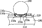
Fig. 3 A is the generalized section of the embodiment 1 of the semiconductor device of the present invention with welding block bottom metalization structure.
This semiconductor device mainly is to comprise semiconductor device body 200, is formed with a plurality of weld pads 210 on this body 200; One protective layer 220 is formed on the surface of this body 200, and is provided with many perforates, makes this weld pad 210 can expose this protective layer 220; A plurality of welding block bottom metalizations (UMB) structure sheaf 230, be coated with on weld pad 210 exposed surfaces of this protective layer 220 around being formed in, it includes a first metal layer 230a, be formed on this weld pad 210, in order to the protective layer 220 around cover part weld pad 210 and the weld pad, one second metal level 230b is formed on this first metal layer 230a, covers the part of solder pads 210 that this first metal layer 230a and all the other are not covered by this first metal layer 230a; At least one the 3rd metal level 230c is formed on this second metal level 230b; And a plurality of welding blocks 240, be formed on this welding block bottom metalization (UMB) structure sheaf 230.
This semiconductor device body 200 is applicable to conductor package substrate construction, also can be used on the general printed circuit board (PCB) (Printed Circuit Board) of second stage assembling electronic device, but best effect is to be applied in semiconductor chip or the wafer that covers crystalline substance (Flip Chip) type.Being formed with a plurality of weld pads 210 on the surface of this semiconductor device body 200, for example can be a copper weld pad, is as the output of these semiconductor body 200 internal circuits, the weld pad of input; Because the structure of these outputs, input weld pad is roughly the same, therefore in order to simplify accompanying drawing and explanation, only shows that a weld pad describes as example.
This protective layer (Passivation Layer) 220 is an insulating barrier (dielectriclayer); in general processing procedure, be to adopt polyimide layer (polyimide layer), silicon dioxide layer (silicon dioxide layer), silicon nitride layer (silicon nitride layer) etc.; in order to cover the surface of this semiconductor device body 200; protect it to avoid external pollution and destruction; and this protective layer 220 has many perforates, to expose this weld pad 210.
This welding block bottom metalization (UMB) structure sheaf 230, include the metal level of multilayer storehouse on this weld pad 210, general is the weld pad 210 that cooperates this metallic copper material in processing procedure, at first be on this copper weld pad 210, to form a first metal layer 230a, titanium coating for example is so as to having good zygosity between weld pad 230 that this metallic copper material is provided and this UBM structure sheaf 230; And the titanium coating of this first metal layer 230a is that part covers weld pad 210 centers that expose this protective layer 220 and centers on this weld pad 210 protective layer 220 upper surfaces on every side, with the annular region of exposing these weld pad 210 upper surfaces and cover protective layer side around this weld pad 210, shown in Fig. 3 B; Simultaneously for strengthening the engaging force of this titanium coating 230a and weld pad 210 and protective layer 220, also can form at least one titanium coating that is connected in weld pad 210 centers partly reaches around the titanium coating connecting portion of the titanium part of these protective layer 220 upper surfaces, shown in Fig. 3 C; Wherein this part covers metal level kind, shape and the quantity of weld pad 210, is not subjected to the restriction shown in this figure, and metal level kind, shape and the quantity that only need provide this UBM structure sheaf 230 to be connected with weld pad 210 all can be applicable among the present invention.
This welding block bottom metalization (UMB) structure sheaf 230 also includes one second metal level 230b, it for example is copper metal layer, be formed on this first metal layer 230a, to cover this first metal layer 230a and all the other part of solder pads 210, can directly contact not by all the other copper weld pads 210 that this titanium coating covered by this copper metal layer, have the excellent electrical property linkage function to provide between this welding block bottom metalization (UMB) structure sheaf 230 and this weld pad 210.On this copper metal layer, also can be coated with one the 3rd metal level 230c; nickel metal layer for example; to provide good environmental protection of coating this copper metal layer wherein and the follow-up welding welding block on it to have the good profit effect of being stained with, this welding block 240 can be connect smoothly put on this welding block bottom metalization (UMB) structure sheaf 230.
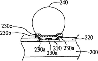
Embodiment 2
See also Fig. 4 A, be the semiconductor device schematic diagram with welding block bottom metalization structure of the embodiment of the invention 2.As shown in the figure, the content that the semiconductor device of the embodiment of the invention 2 and embodiment 1 are disclosed is roughly the same, its difference is in when this welding block bottom metalization (UMB) structure sheaf 230 of preparation, this the first metal layer 230a, titanium coating for example, be that part covers weld pad 210 centers of exposing this protective layer and centers on this weld pad 210 protective layer 220 upper surfaces and side on every side, only expose the annular section of these weld pad 210 outer surfaces, shown in Fig. 4 B, further by strengthening this titanium gold layer area, to increase the joint capacity of this UBM structure sheaf 230 and protective layer 220 and this weld pad 210; Have, the titanium coating that also can form these weld pad 210 centers of at least one connection partly reaches around the titanium coating connecting portion of the titanium part on these protective layer 220 surfaces, shown in Fig. 4 C again.
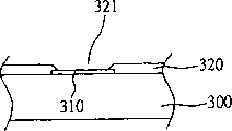
See also Fig. 5 A Fig. 5 E, have the semiconductor device processing procedure generalized section of welding block bottom metalization structure for embodiments of the invention 2.
Shown in Fig. 5 A; at first one protective layer 320 is arranged in semiconductor chip 300 surface coverage that are pre-formed a plurality of copper weld pads 310; silicon dioxide layer for example; and make this protective layer 320 only cover the circumferential surface of this weld pad 310 at these weld pad 310 places, make this protective layer 320 have many perforates 321 of exposing these weld pad 310 cores.
Shown in Fig. 5 B, then on this protective layer 320, utilize sputter (sputtering) technology to be formed with the first gold medal layer, for example titanium coating 330a.
Shown in Fig. 5 C; carry out etching (etching) at the titanium coating 330a that covers this protective layer 320 again; this titanium coating is formed with on these copper weld pad 310 surfaces just like shown in Fig. 4 B; cover this weld pad 310 in order to part and reach the figure on protective layer 320 surfaces on every side; have the good bond ability to utilize between this titanium coating 330a and the copper weld pad 310, good bond effect between this protective layer 320 and this weld pad 310 is provided.
Shown in Fig. 5 D, then finish the titanium coating 330a surface of patterning at this, electroplate the second metal level 330b and the 3rd metal level 330c, for example be copper metal layer 330b and nickel metal layer 330c, make this copper metal layer 330b can cover the part of solder pads 310 that is not covered by this titanium coating 330a, with this copper weld pad 310 of direct contact, make again that this nickel metal layer 330c is complete to be covered on this copper metal layer 330b, to finish this welding block bottom metalization (UMB) structure sheaf 330.
Shown in Fig. 5 E, on this welding block bottom metalization (UMB) structure sheaf 330, be coated with a scolder at last, and form a welding block 340, to finish the semiconductor device with welding block bottom metalization structure of the present invention through back welding process.
Because being part, this titanium coating covers on this copper weld pad; to keep the joint capacity of this ubm structure layer and protective layer and this weld pad; this titanium coating is not to cover fully on this copper weld pad simultaneously; make the follow-up copper metal layer that is formed on the titanium coating can directly contact this copper weld pad, to keep the excellent electrical property linkage function simultaneously.
Claims (18)
1. the semiconductor device with welding block bottom metalization structure is characterized in that, this semiconductor device comprises:
The semiconductor device body, and be formed with a plurality of weld pads at this body surface;
One protective layer is the surface that covers this semiconductor device body, and is formed with many perforates to expose outside this weld pad;
A plurality of welding block bottom metalization structure sheafs, this welding block bottom metalization structure sheaf comprises a plurality of metal levels and is coated with on the weld pad exposed surface of this protective layer with around being formed on, wherein the first metal layer is formed on this weld pad, in order to cover part of solder pads and weld pad protective layer on every side, second metal level is formed on this first metal layer, covers this first metal layer and besides is exposed at the part of solder pads of this first metal layer; And
A plurality of welding blocks are formed on this welding block bottom metalization structure sheaf.
2. semiconductor device as claimed in claim 1 is characterized in that, this welding block bottom metalization structure sheaf also includes at least one the 3rd metal level and covers on this second metal level.
3. semiconductor device as claimed in claim 1 is characterized in that, this semiconductor device body is any in semiconductor chip, wafer, conductor package substrate and the circuit board.
4. semiconductor device as claimed in claim 1 is characterized in that, the material of this weld pad is a metallic copper.
5. semiconductor device as claimed in claim 1 is characterized in that, the material of this first metal layer is a Titanium.
6. semiconductor device as claimed in claim 1 is characterized in that, the material of this second metal level is a metallic copper.
7. semiconductor device as claimed in claim 2 is characterized in that, the material of the 3rd metal level is a metallic nickel.
8. semiconductor device as claimed in claim 1 is characterized in that, this protective layer is an insulating barrier.
9. semiconductor device as claimed in claim 8 is characterized in that, the material of this protective layer is any in polyimide layer, silicon dioxide layer and the silicon nitride layer.
10. the semiconductor device processing procedure with welding block bottom metalization structure is characterized in that, this semiconductor device processing procedure comprises:
At first cover a protective layer, and this protective layer have many perforates to expose this weld pad at least one semiconductor device body surface that is formed with a plurality of weld pads;
At this protective layer and expose to the open air on the weld pad of this protective layer perforate and form the first metal layer, and this first metal layer of patterning, this the first metal layer is partly covered on this weld pad and the weld pad protective layer on every side, on this first metal layer, form second metal level again, make this second metal level cover this first metal layer and all the other outer part of solder pads that is exposed at this first metal layer, constituted the welding block bottom metalization structure sheaf that covers on this weld pad; And
On this welding block bottom metalization structure sheaf, form a welding block.
11. semiconductor device processing procedure as claimed in claim 10 is characterized in that, also is formed with at least one the 3rd metal level on this second metal level.
12. semiconductor device processing procedure as claimed in claim 10 is characterized in that, this semiconductor device body is any in semiconductor chip and the wafer.
13. semiconductor device processing procedure as claimed in claim 10 is characterized in that, the material of this weld pad is a metallic copper.
14. semiconductor device processing procedure as claimed in claim 10 is characterized in that, the material of this first metal layer is a Titanium.
15. semiconductor device processing procedure as claimed in claim 10 is characterized in that, the material of this second metal level is a metallic copper.
16. semiconductor device processing procedure as claimed in claim 11 is characterized in that, the material of the 3rd metal level is a metallic nickel.
17. semiconductor device processing procedure as claimed in claim 10 is characterized in that, this protective layer is an insulating barrier.
18. semiconductor device processing procedure as claimed in claim 17 is characterized in that, the material of this protective layer is any in polyimide layer, silicon dioxide layer and the silicon nitride layer.
Priority Applications (1)
| Application Number | Priority Date | Filing Date | Title |
|---|---|---|---|
| CNB021533261A CN1237580C (en) | 2002-11-25 | 2002-11-25 | Semiconductor device with welding block button metallization structure and mfg process |
Applications Claiming Priority (1)
| Application Number | Priority Date | Filing Date | Title |
|---|---|---|---|
| CNB021533261A CN1237580C (en) | 2002-11-25 | 2002-11-25 | Semiconductor device with welding block button metallization structure and mfg process |
Publications (2)
| Publication Number | Publication Date |
|---|---|
| CN1503328A CN1503328A (en) | 2004-06-09 |
| CN1237580C true CN1237580C (en) | 2006-01-18 |
Family
ID=34235100
Family Applications (1)
| Application Number | Title | Priority Date | Filing Date |
|---|---|---|---|
| CNB021533261A Expired - Fee Related CN1237580C (en) | 2002-11-25 | 2002-11-25 | Semiconductor device with welding block button metallization structure and mfg process |
Country Status (1)
| Country | Link |
|---|---|
| CN (1) | CN1237580C (en) |
Families Citing this family (4)
| Publication number | Priority date | Publication date | Assignee | Title |
|---|---|---|---|---|
| TWI395279B (en) | 2009-12-30 | 2013-05-01 | Ind Tech Res Inst | Micro-bump structure |
| CN102222653A (en) * | 2010-04-15 | 2011-10-19 | 财团法人工业技术研究院 | Dimpling block structure |
| CN110349870A (en) * | 2018-04-04 | 2019-10-18 | 中芯国际集成电路制造(天津)有限公司 | Wafer stage chip encapsulating structure and preparation method thereof |
| US11682640B2 (en) | 2020-11-24 | 2023-06-20 | International Business Machines Corporation | Protective surface layer on under bump metallurgy for solder joining |
-
2002
- 2002-11-25 CN CNB021533261A patent/CN1237580C/en not_active Expired - Fee Related
Also Published As
| Publication number | Publication date |
|---|---|
| CN1503328A (en) | 2004-06-09 |
Similar Documents
| Publication | Publication Date | Title |
|---|---|---|
| TWI244184B (en) | Semiconductor device with under bump metallurgy and method for fabricating the same | |
| KR100454381B1 (en) | Semiconductor device and manufacturing method thereof | |
| KR100806158B1 (en) | Semiconductor device | |
| US7338891B2 (en) | Semiconductor chip, mounting structure thereof, and methods for forming a semiconductor chip and printed circuit board for the mounting structure thereof | |
| JP3393755B2 (en) | Interconnection structure by reflow solder ball with low melting point metal cap | |
| TWI451822B (en) | Circuit board, semiconductor device, and method of manufacturing semiconductor device | |
| US20030036256A1 (en) | Integrated circuit with bonding layer over active circuitry | |
| US6551854B2 (en) | Semiconductor device having bump electrodes and method of manufacturing the same | |
| KR100536036B1 (en) | Semiconductor device | |
| KR20020044590A (en) | Metal redistribution layer having solderable pads and wire bondable pads | |
| US20040232540A1 (en) | Electronic device and method of manufacturing the same, circuit board, and electronic instrument | |
| JP4021104B2 (en) | Semiconductor device having bump electrodes | |
| TW200529384A (en) | Semiconductor device and method of manufacturing the same | |
| JPH02272737A (en) | Projecting electrode structure of semiconductor and formation of projecting electrode | |
| JP5248868B2 (en) | Brazeable joint and method for forming the joint | |
| CN1211000C (en) | Rigidity flexible base board and camera using the same | |
| WO2006070808A1 (en) | Semiconductor chip and method for manufacturing same, electrode structure of semiconductor chip and method for forming same, and semiconductor device | |
| CN1316581C (en) | Encapsulated pin structure for improved reliability of wafer | |
| CN1237580C (en) | Semiconductor device with welding block button metallization structure and mfg process | |
| KR20200035197A (en) | Semiconductor device and method for manufacturing the same | |
| US7202421B2 (en) | Electronic elements, method for manufacturing electronic elements, circuit substrates, method for manufacturing circuit substrates, electronic devices and method for manufacturing electronic devices | |
| JP3700598B2 (en) | Semiconductor chip, semiconductor device, circuit board, and electronic equipment | |
| TWI223425B (en) | Method for mounting passive component on wafer | |
| JP3564311B2 (en) | Method for manufacturing semiconductor wafer with columnar electrode and method for manufacturing semiconductor device | |
| US6692629B1 (en) | Flip-chip bumbing method for fabricating solder bumps on semiconductor wafer |
Legal Events
| Date | Code | Title | Description |
|---|---|---|---|
| C06 | Publication | ||
| PB01 | Publication | ||
| C10 | Entry into substantive examination | ||
| SE01 | Entry into force of request for substantive examination | ||
| C14 | Grant of patent or utility model | ||
| GR01 | Patent grant | ||
| C17 | Cessation of patent right | ||
| CF01 | Termination of patent right due to non-payment of annual fee |
Granted publication date: 20060118 Termination date: 20091225 |