CN1231780A - Voltage controlled variable current reference - Google Patents
Voltage controlled variable current reference Download PDFInfo
- Publication number
- CN1231780A CN1231780A CN97198322A CN97198322A CN1231780A CN 1231780 A CN1231780 A CN 1231780A CN 97198322 A CN97198322 A CN 97198322A CN 97198322 A CN97198322 A CN 97198322A CN 1231780 A CN1231780 A CN 1231780A
- Authority
- CN
- China
- Prior art keywords
- current
- voltage
- electric current
- source
- output
- Prior art date
- Legal status (The legal status is an assumption and is not a legal conclusion. Google has not performed a legal analysis and makes no representation as to the accuracy of the status listed.)
- Pending
Links
Images

Classifications
-
- H—ELECTRICITY
- H03—ELECTRONIC CIRCUITRY
- H03K—PULSE TECHNIQUE
- H03K19/00—Logic circuits, i.e. having at least two inputs acting on one output; Inverting circuits
- H03K19/02—Logic circuits, i.e. having at least two inputs acting on one output; Inverting circuits using specified components
- H03K19/08—Logic circuits, i.e. having at least two inputs acting on one output; Inverting circuits using specified components using semiconductor devices
- H03K19/094—Logic circuits, i.e. having at least two inputs acting on one output; Inverting circuits using specified components using semiconductor devices using field-effect transistors
-
- G—PHYSICS
- G05—CONTROLLING; REGULATING
- G05F—SYSTEMS FOR REGULATING ELECTRIC OR MAGNETIC VARIABLES
- G05F3/00—Non-retroactive systems for regulating electric variables by using an uncontrolled element, or an uncontrolled combination of elements, such element or such combination having self-regulating properties
- G05F3/02—Regulating voltage or current
- G05F3/08—Regulating voltage or current wherein the variable is dc
- G05F3/10—Regulating voltage or current wherein the variable is dc using uncontrolled devices with non-linear characteristics
- G05F3/16—Regulating voltage or current wherein the variable is dc using uncontrolled devices with non-linear characteristics being semiconductor devices
- G05F3/20—Regulating voltage or current wherein the variable is dc using uncontrolled devices with non-linear characteristics being semiconductor devices using diode- transistor combinations
- G05F3/26—Current mirrors
- G05F3/262—Current mirrors using field-effect transistors only
Landscapes
- Engineering & Computer Science (AREA)
- Physics & Mathematics (AREA)
- Microelectronics & Electronic Packaging (AREA)
- Radar, Positioning & Navigation (AREA)
- Electromagnetism (AREA)
- General Physics & Mathematics (AREA)
- Nonlinear Science (AREA)
- Automation & Control Theory (AREA)
- Power Engineering (AREA)
- Computer Hardware Design (AREA)
- Computing Systems (AREA)
- General Engineering & Computer Science (AREA)
- Mathematical Physics (AREA)
- Control Of Electrical Variables (AREA)
- Electronic Switches (AREA)
Abstract
A current source providing a voltage-controlled variable current reference is described which employs a conventional current mirror (20) to supply a current (Im) to a diode-connected transistor (22), and to a plurality of controllable current paths (30), wherein the controllable current paths (30) are controlled by voltages from a voltage sensing circuit (26) so that predetermined amounts of current are drawn away from the diode-connected transistor (22) as a function of a controlled voltage, so that the diode-connected transistor (22) generates a voltage as a function of the current (Im) flowing through it, which voltage is used to control an output transistor (12) and a current (Io) flowing through the output transistor (12).
Description
Technical field
The present invention is target with the current source, is target with the voltage-controlled variable current reference circuit particularly.
Technical background
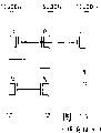
The typical current source is described current mirror in the prior art, wherein, reference current is forced to the bipolar or MOS transistor that the diode of flowing through connects, then, be provided for the base of the transistor seconds of similar structures-penetrate or grid-two ends, source at described transistorized base-penetrate or grid-voltage that the two ends, source cause.This produces the electric current through the transistor seconds relevant with the electric current of the first transistor of flowing through again.Usually, when the power supply of described current mirror from full voltage when zero volt changes, the amplitude of the electric current that flows out from described current mirror reduces.This typical current mirror is in Figure 1A, and wherein the variation of electric current is the function of the described power supply of Figure 1B.
In some applications, hope can provide and not consider current source mains voltage variations, that stabling current can be provided.In other are used, wish that described current source has to control in a predefined manner so that it becomes the output current of the function of mains voltage variations.In addition, some the time also wish to have a current source, wherein, output current can increase or reduce as the function that is applied in to the reference voltage of described current source.
Summary of the invention
The invention provides a kind of stable current source that can in the wide power voltage range, move and can increase or reduce as the function of supply voltage or the reference voltage that the user provided.According to the present invention, a current source is provided, this current source is accepted energy and is comprised the current source that the scheduled volume electric current can be provided from supply voltage.First semiconductor device is coupled to receive from the electric current of described current source and the output voltage that has selected relation with respect to the current amplitude that receives from described current source is provided.A plurality of controllable currents path be connected with receive from the electric current of described current source output and when being activated each in described a plurality of controllable currents path be configured to hold the selected magnitude of current.Voltage reading circuit is coupled receiving a control voltage, and activates a part in described a plurality of controllable currents path as the function that described control voltage magnitude changes.Second semiconductor device is coupled to receive from the voltage of first semiconductor device output and the output current that has selected relation with respect to the output voltage amplitude that receives from described first device is provided.Utilize this mode, when the controllable current path of varying number is activated by described voltage reading circuit, flow out more or less electric current, flow into the magnitude of current of first semiconductor device whereby with influence from first semiconductor device.This causes being formed by first semiconductor device, and offers the variation of the output voltage of second semiconductor device.Then, the output current that provides by second semiconductor device function that will change as the output voltage that receives from first device and changing.
In each embodiment of the present invention, described voltage reading circuit can be coupled on the power supply, perhaps is coupled on the reference voltage that the user provides.In addition, can use two voltage reading circuits, one of them is coupled on the described power supply, and another is coupled to receive control or the reference voltage from the user.
Therefore an object of the present invention is to provide a kind of current source, this current source provides can be by the output current of selected voltage source control.
Another object of the present invention provides a kind of voltage-controlled variable current source, and wherein, the amplitude of output current is to control by the amplitude that changes the control voltage that is applied.
Following detailed description in conjunction with the drawings, these and other objects of the present invention, characteristic and advantage are with easier to understand.
The accompanying drawing summary
Figure 1A shows traditional current mirror briefly.
The electric current change curve as the supply voltage function that is provided by current mirror shown in Figure 1A is provided Figure 1B.
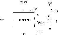
Fig. 2 shows the high level functional block diagram of one embodiment of the invention.
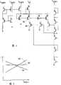
Fig. 3 shows one embodiment of the present of invention briefly, and in this embodiment, output current is controlled as the function of described supply voltage.
Fig. 4 shows an alternative embodiment of the invention briefly, and in this embodiment, output current is controlled as the function of a supply voltage and a reference voltage.
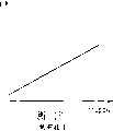
Fig. 5 shows the simplification curve as the different output current variation of the supply voltage function that can obtain according to the present invention.
Fig. 6 shows another embodiment of the present invention, and in this embodiment, output current is controlled with the increase with supply voltage to be increased.
Describe in detail
Referring to Fig. 2, from conceptive description the present invention.Usually, the present invention includes an output device 12, be used for providing output current as the function of the control voltage that imposes on control end 16 at output 14 places.In a most preferred embodiment of the present invention, described output device 12 is MOS transistor.
Being used for providing the control circuit 18 of control voltage to output device 12 is by supply voltage V
SupplyEnergy supply, and can be by a reference voltage V
RefControl.According to the present invention, along with V
SupplyAnd V
RefVariation, the control voltage V that provides by control circuit 18
ControlChange with a kind of predetermined way.
Referring now to Fig. 3,, will do detailed description to an embodiment of control circuit 18.In the embodiment shown in fig. 3, control circuit 18 comprises a traditional current mirror 20, and this current mirror 20 provides electric current to the transistor 22 that diode connects.Be connected on the transistor 22 that diode connects is one group of controllable current path 24.In these controllable current paths each all is voltage-controlled by what provide from voltage reading circuit 26.
In Fig. 3, from the current i of current mirror 20
mFlow into the transistor 22 that diode connects.This has introduced a voltage on online 16, and this voltage is provided for the control gate of transistor 12 with the output current i to the transistor 12 of flowing through
OutControl.When being activated, one group of selectable current path 24 draws electric current and makes it flow out the transistor 22 that diode connects from current mirror 20.This has reduced the voltage level on the line 16, has next reduced to offer the control voltage of transistor 12 again, and has therefore reduced output current i
Out
In current path described in the described group of current path 24 each all is by voltage-controlled from of voltage reading circuit 26.Specifically, voltage reading circuit 26 is to be formed by the trapezium structure that the transistor that a plurality of diodes connect constitutes.Should illustrate that each in the controllable current path 30 is connected on the different nodes of described trapezium structure, thereby in these paths each will be activated according to the amplitude of the supply voltage that provides at described trapezium structure summit place.For example, work as V
SupplyBe 3 threshold value V of level above Ground
TThe time, will be activated by the voltage-controlled described controllable current path at node 32 places.Next, work as V
SupplyWhen being 4 threshold voltages of level above Ground, the controllable current path of being controlled by the node 34 of voltage reading circuit 26 30 will be activated.Should be appreciated that the magnitude of current that flows out can be controlled so as to supply voltage V by described controllable current path being connected on the difference in voltage reading circuit 26 trapezium structures from the transistor 22 that diode connects
SupplyThe function of amplitude.It should also be understood that, the transistorized threshold voltage that diode in voltage reading circuit 26 connects (for example can be formed the value different with transistor threshold voltage in controlled path 30, by changing described transistorized physical size), thus other variation in can obtaining to control.
One group 24 of discussion controllable current path 30 now, each of controllable current path 30 preferably all is configured to the transistor that pair of series connects, transistor 22 parallel connections that every pair of transistor AND gate diode in these transistors connects.A transistor drain in the described pair of transistor is connected in the drain electrode of the transistor 22 that described diode connects, and its grid is connected on the grid of the transistor 22 that described diode connects.The drain electrode of transistor seconds is connected to the source electrode of the first transistor, and its source ground, its control gate are used to receive the corresponding control voltage from voltage reading circuit 26.
The size that should be appreciated that the first transistor 36 can be configured to absorb the electric current of conduct at the predetermined quantity of the gate source voltage function of transistor 22 two ends introducing from current mirror 20.For example, for the given gate source voltage in transistor 22 two ends that connects at diode, for the identical gate source voltage that transistor 22 two ends that connect at diode provide, the size of transistor 36 can be configured to draw its electric current of 1/10 from the electric current of the transistor 22 of flowing through.
Thus, clearly, under this condition, if in one group of controllable current path 24, provide 10 controllable current paths, the activation in all these paths will be drawn from current mirror 20 and be flowed out identical electric current a considerable amount of electric currents and the transistor 22 that is connected from diode, make voltage V on the line 16 whereby
ControlSignificantly reduced.Next, can see and work as V
SupplyDuring decline, will there be controllable current path still less to be activated, whereby, have increased the magnitude of current that allows to flow to the transistor 22 of diode connection from current mirror 20, thus the voltage magnitude at line 16 places that raise and the electric current that has increased the transistor 12 of flowing through.In this manner, reduce supply voltage will cause the flowing through increase of output current of transistor 12.On the contrary, work as V
SupplyDuring increase, the magnitude of current of the minimizing transistor 22 that diode connects that is allowed to flow through makes that whereby online 16 places appear in the voltage magnitude that is reduced.Then, the amplitude of the output current that is provided by transistor 12 reduces along with the increase of supply voltage.
Referring now to Fig. 4,, except second group of controllable current path 40 and the second voltage reading circuit 42 be coupled with, circuit shown in this figure and circuit shown in Figure 3 were similar.The formation of voltage reading circuit 42 is similar to voltage reading circuit 36, but is coupled on the reference voltage that can be provided by the user.In addition, should illustrate that compare with voltage reading circuit 26, control voltage is taken from the different nodes of voltage reading circuit 42.This means needs voltage V
RefDifferent amplitudes activate different paths in second group of controllable current path 40.
According to Fig. 3 and Fig. 4, clearly, utilize transistor and the controllable current path 30 and the node of selecting to obtain in the voltage reading circuit 26 control voltage of appropriate size, the magnitude of current of the transistor 22 that permission inflow diode connects can be controlled as desired.For example, can stipulate in the controllable current path 30 transistorized size and select the control voltages, thereby an output current is provided that when the level of described supply voltage changed, the variation of this output current was not obvious from voltage reading circuit 26.Specifically, when the amplitude of supply voltage reduced, less electric current was drawn with Be Controlled in the controllable current path, and the speed that can select this minimizing to take place reduces current i to remedy current mirror 20 with the minimizing of supply voltage
mThe speed of amplitude.Utilize this mode, even under the situation that supply voltage reduces, the electric current of the transistor 22 that the diode of flowing through connects also can roughly keep identical.
Wishing that in fact output current reduces under the situation about increasing with supply voltage, can select the transistor (with control electrical voltage point) in the controllable current path 24, so that the magnitude of current that is allowed to flow into the transistor 22 that diode connects is higher than at the low supply voltage place than the high power supply voltage place from voltage reading circuit 26.Referring to Fig. 5, this state of the latter is by curve 44 expressions.Similarly, the electric current of the transistor 22 of inflow diode connection keeps constant situation to be shown in the curve 46 of Fig. 5 during whole power source change.
Referring now to Fig. 6,, the figure shows one embodiment of the present of invention, in this embodiment, output current i
OutIncrease along with the increase of supply voltage.Fig. 3 and 4 differences with respect to Fig. 6 are that in the former controllable current path, transistor 36 and 38 is N-channel transistors.On the contrary, in Fig. 6, transistor 36 is N-channel transistors, and N-channel transistor 38 is replaced by P-channel transistor 48.
Work as V
SupplyWhen being low, all controllable current paths are switched on, and work as V
SupplyAmplitude when increasing, described controllable current path is closed.In this manner, the electric current that is allowed to flow into the transistor 22 that diode connects increases along with the increase of supply voltage.The output current of Fig. 6 and the relation of supply voltage are shown in the curve among Fig. 5 50.
Should be appreciated that when above-mentioned accompanying drawing has shown some embodiment, can also be formed in many other variations within the spirit of the present invention.When the example that has provided is metal oxide semiconductor transistor, can also use bipolar transistor and other device.
Here employed term and expression only are used as the term that is used to describe and not as restriction, in the use of these terms and expression, the equivalent of characteristic and description or its part shown in not attempting to get rid of, will be appreciated that various modifications all are possible in the scope of claims of the present invention.
Claims (18)
1. one kind is used to provide output current and obtains the current source of energy from power supply, comprising:
An output device, be used between first and second outputs, providing electric current and have a control end, wherein, the amplitude of the output current that flows between first and second outputs is used as the function that is applied in to a voltage of described control end and controls;
Be coupled on the described power supply and provide the control circuit of a control voltage to the control end of described output device, described control voltage changes as power supply amplitude function in a predefined manner, and wherein, described control circuit comprises:
A semiconductor device is used to produce the voltage as the function of a current amplitude that flows through it; With
The function that a plurality of current paths, these paths can be used as a reference voltage amplitude is activated and revises the current amplitude of the described semiconductor device of flowing through.
2. current source according to claim 1 is characterized in that described output device is a field-effect transistor.
3. current source according to claim 1, it is characterized in that described control circuit comprises having the source that its output is coupled to an electric current on the described output device control end, wherein, the source of described electric current provides the electric current of predetermined quantity, and described first semiconductor device is coupled with received current from the output in the source of described electric current and can produces the voltage that the amplitude of an electric current that receives with respect to the source from described electric current has choice relation at the output in the source of described electric current; Wherein, each in described a plurality of current paths is connected with received current from the output in the source of described electric current, and when being activated, wherein each all is configured to hold the electric current of selected quantity; Also comprise:
Be coupled to described power supply and activate the described controllable current of part path changes function as the power supply amplitude a voltage reading circuit.
4. current source according to claim 1, the source that it is characterized in that described electric current are current mirrors.
5. current source according to claim 1 is characterized in that in described a plurality of controllable currents path each comprises a plurality of field-effect transistors.
6. current source according to claim 5 is characterized in that described a plurality of controllable currents path comprises:
The metal oxide semiconductor transistor that diode connects;
The metal oxide semiconductor transistor that is connected with described diode is connected in series and has and is coupled so that second metal oxide semiconductor transistor of a control gate of being controlled by described control circuit.
7. current source according to claim 1 is characterized in that described voltage reading circuit comprises a plurality of be connected in series in echelon and a end that this is trapezoidal is coupled to the field-effect transistor that the diode on the described power supply connects; Wherein, the node between the field-effect transistor of some described diodes connections is provided for controlling the control voltage in described a plurality of controllable currents path.
8. the current source from the power supply energy supply comprises;
Be used to provide the source of the electric current of predetermined quantity electric current;
Be coupled to receive from the electric current in the source of described electric current and first semiconductor device that provides the amplitude of the electric current that receives with respect to source to have selected relation from described electric current;
Be connected a plurality of controllable currents path, can hold the electric current of selected quantity when each in described a plurality of controllable currents path is configured to be activated with received current from the output in the source of described electric current;
Be coupled to receive the voltage reading circuit controlling voltage and activate the described controllable current of part path as the function that described control voltage magnitude changes; With
Be coupled to receive from the output voltage of described first device and second semiconductor device that has the output current of selected relation with respect to the output voltage amplitude that receives from described first device is provided.
9. current source according to claim 8 is characterized in that described first and second semiconductor device are field-effect transistors and wherein, and described first semiconductor device is the structure that diode connects.
10. current source according to claim 8, the source that it is characterized in that described electric current are current mirrors.
11. current source according to claim 8 is characterized in that in described a plurality of controllable currents path each comprises a plurality of field-effect transistors.
12. current source according to claim 11 is characterized in that described a plurality of controllable currents path comprises:
The metal oxide semiconductor transistor that diode connects;
The metal oxide semiconductor transistor that is connected with described diode series connection and having is coupled so that second metal oxide semiconductor transistor of the control gate of being controlled by described control circuit.
13. current source according to claim 8 is characterized in that described voltage reading circuit comprises a plurality of field-effect transistors that an end trapezoidal and that this is trapezoidal is coupled to the diode connection on the described power supply that are serially connected in; Wherein, the node between the field-effect transistor of some described diodes connections is provided for controlling the control voltage in described a plurality of controllable currents path.
14. one kind is used to provide output current and from the current source of power supply energy supply, comprises:
The output device that is used between first and second outputs, providing output current and has a control end, wherein, the amplitude of the output current that flows between described first and second outputs is controlled as the function of a voltage that imposes on described control end;
Have the source of electric current of the output of the control end that is coupled to described output device, wherein, the source of described electric current provides the electric current of scheduled volume;
Be coupled to receive and produce first semiconductor device that current amplitude that its amplitude receives with respect to the source from described electric current has the voltage of selected relation from the output current in the source of described electric current and output in the source of described electric current;
Be connected with a plurality of controllable currents path from the output received current in the source of described electric current, each in described a plurality of controllable currents path is configured to can hold the electric current of selected amount when being activated;
Activate the described controllable current of part path and make thereby be coupled to described power supply and change function at the voltage level control flows of the output in the source of described electric current a voltage reading circuit through the output current of described output device as the power supply amplitude.
15. current source according to claim 14, the source that it is characterized in that described electric current are current mirrors.
16. current source according to claim 14 is characterized in that each path in described a plurality of controllable currents path comprises a plurality of field-effect transistors.
17. current source according to claim 16 is characterized in that described a plurality of controllable currents path comprises:
The metal oxide semiconductor transistor that diode connects;
The metal oxide semiconductor transistor that is connected with described diode series connection and having is coupled so that by second metal oxide semiconductor transistor of a control gate of described control circuit control.
18. current source according to claim 14 is characterized in that described voltage reading circuit comprises a plurality of field-effect transistors that a trapezoidal diode connects that are serially connected in, this trapezoidal end is coupled on the described power supply; Wherein, the node between the field-effect transistor that some diodes connect be provided for controlling described a plurality of controllable currents path control voltage.
Applications Claiming Priority (2)
| Application Number | Priority Date | Filing Date | Title |
|---|---|---|---|
| US08/690,008 US5793248A (en) | 1996-07-31 | 1996-07-31 | Voltage controlled variable current reference |
| US08/690,008 | 1996-07-31 |
Publications (1)
| Publication Number | Publication Date |
|---|---|
| CN1231780A true CN1231780A (en) | 1999-10-13 |
Family
ID=24770727
Family Applications (1)
| Application Number | Title | Priority Date | Filing Date |
|---|---|---|---|
| CN97198322A Pending CN1231780A (en) | 1996-07-31 | 1997-07-24 | Voltage controlled variable current reference |
Country Status (8)
| Country | Link |
|---|---|
| US (1) | US5793248A (en) |
| EP (1) | EP0916187A4 (en) |
| JP (1) | JP2001500997A (en) |
| KR (1) | KR100414596B1 (en) |
| CN (1) | CN1231780A (en) |
| AU (1) | AU3892497A (en) |
| CA (1) | CA2261733A1 (en) |
| WO (1) | WO1998005125A1 (en) |
Cited By (1)
| Publication number | Priority date | Publication date | Assignee | Title |
|---|---|---|---|---|
| CN101694963B (en) * | 2009-09-22 | 2013-09-18 | 美芯晟科技(北京)有限公司 | High-precision low-voltage voltage/current switching circuit |
Families Citing this family (17)
| Publication number | Priority date | Publication date | Assignee | Title |
|---|---|---|---|---|
| US5793248A (en) * | 1996-07-31 | 1998-08-11 | Exel Microelectronics, Inc. | Voltage controlled variable current reference |
| GB9920080D0 (en) * | 1999-08-24 | 1999-10-27 | Sgs Thomson Microelectronics | Current reference circuit |
| US7222208B1 (en) | 2000-08-23 | 2007-05-22 | Intel Corporation | Simultaneous bidirectional port with synchronization circuit to synchronize the port with another port |
| US6445170B1 (en) | 2000-10-24 | 2002-09-03 | Intel Corporation | Current source with internal variable resistance and control loop for reduced process sensitivity |
| US6448811B1 (en) * | 2001-04-02 | 2002-09-10 | Intel Corporation | Integrated circuit current reference |
| US6522174B2 (en) * | 2001-04-16 | 2003-02-18 | Intel Corporation | Differential cascode current mode driver |
| US6791356B2 (en) * | 2001-06-28 | 2004-09-14 | Intel Corporation | Bidirectional port with clock channel used for synchronization |
| US6529037B1 (en) | 2001-09-13 | 2003-03-04 | Intel Corporation | Voltage mode bidirectional port with data channel used for synchronization |
| US6597198B2 (en) | 2001-10-05 | 2003-07-22 | Intel Corporation | Current mode bidirectional port with data channel used for synchronization |
| US6693332B2 (en) * | 2001-12-19 | 2004-02-17 | Intel Corporation | Current reference apparatus |
| GB0211564D0 (en) * | 2002-05-21 | 2002-06-26 | Tournaz Technology Ltd | Reference circuit |
| US20050003764A1 (en) * | 2003-06-18 | 2005-01-06 | Intel Corporation | Current control circuit |
| KR100613574B1 (en) * | 2004-05-06 | 2006-08-16 | 매그나칩 반도체 유한회사 | Current-voltage amplifier |
| DK1635240T3 (en) * | 2004-09-14 | 2010-06-07 | Dialog Semiconductor Gmbh | Dynamic transconductance boosting techniques for power mirrors |
| TW200928648A (en) * | 2007-12-20 | 2009-07-01 | Airoha Tech Corp | Voltage reference circuit |
| CN101557669B (en) * | 2009-03-11 | 2012-10-03 | 深圳市民展科技开发有限公司 | High precision controllable current source |
| CN102622957B (en) * | 2011-02-01 | 2014-07-02 | 北京大学 | Multichannel LED constant current source driving circuit based on MOSFET of linear region with constant grid voltage |
Family Cites Families (9)
| Publication number | Priority date | Publication date | Assignee | Title |
|---|---|---|---|---|
| JPS5672350A (en) * | 1979-11-19 | 1981-06-16 | Advantest Corp | Variable current source |
| JPS5750139A (en) * | 1980-09-10 | 1982-03-24 | Toshiba Corp | Hysteresis circuit |
| US4608530A (en) * | 1984-11-09 | 1986-08-26 | Harris Corporation | Programmable current mirror |
| US4864162A (en) * | 1988-05-10 | 1989-09-05 | Grumman Aerospace Corporation | Voltage variable FET resistor with chosen resistance-voltage relationship |
| JPH06343022A (en) * | 1993-06-01 | 1994-12-13 | Fujitsu Ltd | Voltage controlled oscillation circuit |
| US5583464A (en) * | 1994-05-13 | 1996-12-10 | Thinking Machines Corporation | Resistor circuit for integrated circuit chip using insulated field effect transistors |
| US5457407A (en) * | 1994-07-06 | 1995-10-10 | Sony Electronics Inc. | Binary weighted reference circuit for a variable impedance output buffer |
| US5483151A (en) * | 1994-09-27 | 1996-01-09 | Mitsubishi Denki Kabushiki Kaisha | Variable current source for variably controlling an output current in accordance with a control voltage |
| US5793248A (en) * | 1996-07-31 | 1998-08-11 | Exel Microelectronics, Inc. | Voltage controlled variable current reference |
-
1996
- 1996-07-31 US US08/690,008 patent/US5793248A/en not_active Expired - Lifetime
-
1997
- 1997-07-24 KR KR10-1999-7000736A patent/KR100414596B1/en not_active IP Right Cessation
- 1997-07-24 CN CN97198322A patent/CN1231780A/en active Pending
- 1997-07-24 CA CA002261733A patent/CA2261733A1/en not_active Abandoned
- 1997-07-24 JP JP10508973A patent/JP2001500997A/en active Pending
- 1997-07-24 EP EP97936194A patent/EP0916187A4/en not_active Withdrawn
- 1997-07-24 WO PCT/US1997/012984 patent/WO1998005125A1/en active Search and Examination
- 1997-07-24 AU AU38924/97A patent/AU3892497A/en not_active Abandoned
Cited By (1)
| Publication number | Priority date | Publication date | Assignee | Title |
|---|---|---|---|---|
| CN101694963B (en) * | 2009-09-22 | 2013-09-18 | 美芯晟科技(北京)有限公司 | High-precision low-voltage voltage/current switching circuit |
Also Published As
| Publication number | Publication date |
|---|---|
| CA2261733A1 (en) | 1998-02-05 |
| KR100414596B1 (en) | 2004-01-13 |
| KR20000029660A (en) | 2000-05-25 |
| JP2001500997A (en) | 2001-01-23 |
| US5793248A (en) | 1998-08-11 |
| EP0916187A4 (en) | 1999-12-29 |
| AU3892497A (en) | 1998-02-20 |
| EP0916187A1 (en) | 1999-05-19 |
| WO1998005125A1 (en) | 1998-02-05 |
Similar Documents
| Publication | Publication Date | Title |
|---|---|---|
| CN1231780A (en) | Voltage controlled variable current reference | |
| KR100297679B1 (en) | Variable stage charge pump | |
| US7420356B2 (en) | Current direction detection circuit and switching regulator having the same | |
| US6188590B1 (en) | Regulator system for charge pump circuits | |
| US6744305B2 (en) | Power supply circuit having value of output voltage adjusted | |
| US4723225A (en) | Programming current controller | |
| US6369556B2 (en) | Power supply control device and method | |
| US11189325B2 (en) | Device and method for data-writing | |
| US5841270A (en) | Voltage and/or current reference generator for an integrated circuit | |
| NL8402764A (en) | CIRCUIT FOR GENERATING A SUBSTRATE PRELIMINARY. | |
| WO1998005125A9 (en) | Voltage controlled variable current reference | |
| US5883504A (en) | Power supply unit | |
| US20100219892A1 (en) | Current limiter circuit | |
| CN1141628C (en) | Semiconductor device | |
| JP2000067592A (en) | Selector switch integrated monolithically and electrically programmable non-volatile memory cell device | |
| KR100290481B1 (en) | Multi-Stage Pulse Generator Circuit for Flash Memory Devices | |
| US6836436B2 (en) | Voltage generator for flash memory device | |
| KR930008658B1 (en) | Voltage level detecting circuit | |
| US7312601B2 (en) | Start-up circuit for a current generator | |
| JPH01311711A (en) | Clip circuit | |
| KR100629962B1 (en) | Drain voltage generation circuit for a flash memory cell | |
| JPH03220818A (en) | Logic circuit | |
| KR19990069223A (en) | Internal Voltage Generation Circuit of Semiconductor Memory Device |
Legal Events
| Date | Code | Title | Description |
|---|---|---|---|
| C06 | Publication | ||
| PB01 | Publication | ||
| C10 | Entry into substantive examination | ||
| SE01 | Entry into force of request for substantive examination | ||
| C02 | Deemed withdrawal of patent application after publication (patent law 2001) | ||
| WD01 | Invention patent application deemed withdrawn after publication |