CN1228908C - Switch synchronization method of parallel converter system. - Google Patents
Switch synchronization method of parallel converter system. Download PDFInfo
- Publication number
- CN1228908C CN1228908C CNB011301783A CN01130178A CN1228908C CN 1228908 C CN1228908 C CN 1228908C CN B011301783 A CNB011301783 A CN B011301783A CN 01130178 A CN01130178 A CN 01130178A CN 1228908 C CN1228908 C CN 1228908C
- Authority
- CN
- China
- Prior art keywords
- timer
- converter
- carrier wave
- slave
- switch
- Prior art date
- Legal status (The legal status is an assumption and is not a legal conclusion. Google has not performed a legal analysis and makes no representation as to the accuracy of the status listed.)
- Expired - Lifetime
Links
Images


Classifications
-
- H—ELECTRICITY
- H02—GENERATION; CONVERSION OR DISTRIBUTION OF ELECTRIC POWER
- H02M—APPARATUS FOR CONVERSION BETWEEN AC AND AC, BETWEEN AC AND DC, OR BETWEEN DC AND DC, AND FOR USE WITH MAINS OR SIMILAR POWER SUPPLY SYSTEMS; CONVERSION OF DC OR AC INPUT POWER INTO SURGE OUTPUT POWER; CONTROL OR REGULATION THEREOF
- H02M3/00—Conversion of dc power input into dc power output
- H02M3/02—Conversion of dc power input into dc power output without intermediate conversion into ac
- H02M3/04—Conversion of dc power input into dc power output without intermediate conversion into ac by static converters
- H02M3/10—Conversion of dc power input into dc power output without intermediate conversion into ac by static converters using discharge tubes with control electrode or semiconductor devices with control electrode
- H02M3/145—Conversion of dc power input into dc power output without intermediate conversion into ac by static converters using discharge tubes with control electrode or semiconductor devices with control electrode using devices of a triode or transistor type requiring continuous application of a control signal
- H02M3/155—Conversion of dc power input into dc power output without intermediate conversion into ac by static converters using discharge tubes with control electrode or semiconductor devices with control electrode using devices of a triode or transistor type requiring continuous application of a control signal using semiconductor devices only
- H02M3/156—Conversion of dc power input into dc power output without intermediate conversion into ac by static converters using discharge tubes with control electrode or semiconductor devices with control electrode using devices of a triode or transistor type requiring continuous application of a control signal using semiconductor devices only with automatic control of output voltage or current, e.g. switching regulators
- H02M3/158—Conversion of dc power input into dc power output without intermediate conversion into ac by static converters using discharge tubes with control electrode or semiconductor devices with control electrode using devices of a triode or transistor type requiring continuous application of a control signal using semiconductor devices only with automatic control of output voltage or current, e.g. switching regulators including plural semiconductor devices as final control devices for a single load
- H02M3/1584—Conversion of dc power input into dc power output without intermediate conversion into ac by static converters using discharge tubes with control electrode or semiconductor devices with control electrode using devices of a triode or transistor type requiring continuous application of a control signal using semiconductor devices only with automatic control of output voltage or current, e.g. switching regulators including plural semiconductor devices as final control devices for a single load with a plurality of power processing stages connected in parallel
-
- H—ELECTRICITY
- H02—GENERATION; CONVERSION OR DISTRIBUTION OF ELECTRIC POWER
- H02J—CIRCUIT ARRANGEMENTS OR SYSTEMS FOR SUPPLYING OR DISTRIBUTING ELECTRIC POWER; SYSTEMS FOR STORING ELECTRIC ENERGY
- H02J1/00—Circuit arrangements for dc mains or dc distribution networks
- H02J1/10—Parallel operation of dc sources
- H02J1/102—Parallel operation of dc sources being switching converters
Abstract
The present invention relates to a switch synchronization method of a parallel converter system. One of converters is used as a mainframe, and the others are used as a slave machine; a first timer and a pulse sending device are arranged in the mainframe converter; a second timer, a pulse edge acquisition device and a synchronous regulator are arranged in the slave machine converter. The converter system carries out switch synchronization according to the following procedures: the first timer arranged in the mainframe converter sends synchronizing pulses to synchronous buses by the pulse sending device at fixed time Tk 1; the second timer arranged in the slave machine converter records time Tx of the synchronous pulse edge, and the time Tx is received from the synchronous buses by the acquisition device; the synchronous regulator regulates the second timer arranged in the slave machine converter to enable the second timer to synchronize with the first timer arranged in the mainframe converter according to the relationship of the Tk 1 and the Tx; then, a switch carrier wave timer arranged in the slave machine converter is regulated according to a predetermination protocol to enable the switch carrier wave timer arranged in the slave machine converter to synchronize with a switch carrier wave timer arranged in the mainframe converter.
Description
Technical field
The present invention relates to parallel converter system, more particularly, when relating to many parallel connection converters composition parallel converter system work, the synchronous method of maintained switch under various operating modes.
Background technology
Shunt chopper is more common at present, and the parallel rectifier system is few, in present parallelly connected reverse converter system, to the switch control of each inverter, adopts following several method usually:
Method one is that shunt chopper is adopted centralized control, and as shown in Figure 1, shunt chopper is by a common controller control, and the switch of described inverter is in full accord, thereby overcomes the high frequency circulation between the shunt chopper.As shown in Figure 2, two shunt choppers are by a common controller control, and the brachium pontis drive waveforms of each inverter comes down to one like this, and it is also identical to be added in inductance voltage waveform before, so there is not high frequency circulation between the inverter filter inductance.It is dumb that but this method has control mode, and control line might be very long, shortcoming such as disturbed easily, just uses on modular shunt chopper at present, generally do not adopt in the parallel connection of high power contravariant device.
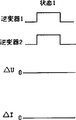
Method two is that shunt chopper is adopted decentralized control, and switching frequency is constant, and high frequency circulation is not handled, and the switch behavior between the inverter is at this moment slided between two states shown in Figure 3.In state shown in Figure 31, when different inverter switching frequencies were synchronous fully, high-frequency electrical pressure reduction was zero between the inverter, so there is not high frequency circulation; In state shown in Figure 32, when different inverter switching device waveforms were reverse fully, high-frequency electrical pressure reduction maximum between the inverter was so high frequency circulation reaches maximum.Sliding frequency between this two states generally needs time several seconds can finish once circulation by the decision of crystal oscillator precision.The shortcoming of this method is that the circulation size changed in a period of time, and in above-mentioned state 2, circulation can be very big, often causes the steady ripple of output voltage big, and fluctuation is arranged, and the filter capacitor electric current is big, causes temperature too high easily.
Method three is that shunt chopper adopts decentralized control, but switching frequency adopts variable frequency control, mainly be to adopt this method at present, it is the variation that the switching frequency of each inverter is not stopping, at this moment in power frequency period, the most of output states of inverter bridge are between Fig. 3 two states, and with the equalization in addition of the high frequency circulation under state shown in Figure 31 and the state 2, the size of its circulation is determined by the inverter filter inductance so in fact.The shortcoming of this method is that switching frequency changes greatly, is not easy control, and still has big high frequency circulation.
Summary of the invention
The technical problem to be solved in the present invention is, above-mentioned defective at prior art, a kind of switch synchronization method of parallel converter system is provided, realize under digitized dispersion Parallel Control, the substantially invariable situation of switching frequency switching frequency between the parallel connection converter synchronously, reduce the high frequency circulation between each converter, help to realize reliable parallel connection.
Technical program of the present invention lies in, construct a kind of switch synchronization method of parallel converter system, it is characterized in that, one of them converter is made as main frame, all the other converters all are made as slave, be provided with a first timer and a pulse transmitter in the described main frame converter, be provided with a second timer, a pulse edge acquisition equipment and a synchronous governor in the described slave converter, it is synchronous that described changer system carries out switch according to the following steps:
First timer in the main frame converter sends lock-out pulse at a fixed time Tk1 by described pulse transmitter on synchronous bus;
Described second timer in the slave converter writes down described acquisition equipment receives described lock-out pulse edge from synchronous bus moment Tx;
Described synchronous governor is implemented synchronized algorithm according to described Tk1 and Tx, regulate second timer in the slave converter make it with the main frame converter in first timer synchronous, press predetermined protocol then and regulate switch carrier wave timer in the slave converter, make it with the main frame converter in switch carrier wave timer synchronous.
According to method of the present invention, when having only a timer in the converter, the first timer while in the main frame converter is as the switch carrier wave timer of this converter; The second timer while in the slave converter is as the switch carrier wave timer of this converter.When described synchronous governor the second timer in the slave converter is adjusted to the main frame converter in first timer synchronous the time, also just realized principal and subordinate's converter switch carrier wave timer synchronously.
According to method of the present invention, also can set up the switch carrier wave timer of a timer as this converter in each converter, the relation between first timer in the main frame converter and the switch carrier wave timer, between the second timer in the slave converter and the switch carrier wave timer is obeyed the first predetermined agreement.Wherein, described first agreement can be stipulated to keep between first timer in the main frame converter and the switch carrier wave timer synchronously; Keep synchronously between second timer in the same slave converter and the switch carrier wave timer.Switch carrier wave timer in also can regulation main frame converter is leading or lag behind set time of first timer; Switch carrier wave timer in the same slave converter is leading or lag behind set time of second timer.
According to method of the present invention, can in described main frame converter, set up a second timer, in described slave converter, set up a first timer simultaneously; First timer in the same converter and second timer keep synchronously, and relation is between the two obeyed the second predetermined agreement.When described synchronous governor the second timer in the slave converter is adjusted to the main frame converter in first timer synchronous the time, first timer in the slave converter also be adjusted to the main frame converter in first timer synchronous, thereby realized principal and subordinate's converter switch carrier wave timer synchronously.
According to method of the present invention, when two timers are arranged in the converter, the described second agreement regulation is configured to dull count mode with second timer, if the first timer in the same converter is configured to rising/decline count mode, then the cycle of second timer is 2 times of first timer cycle; If the first timer in the same converter is configured to dull the rising or dull decline count mode, then the cycle of second timer is identical with the cycle of first timer.
According to method of the present invention, when two timers were arranged in the converter, the first timer while in each converter was as the switch carrier wave timer of this converter.
Method of the present invention is applied in the parallel UPS, can realizes effectively that switch keeps suppressing the high frequency circulation between the parallel connection converter synchronously between the parallel connection converter.
The invention will be further described below in conjunction with drawings and Examples.
Description of drawings
Fig. 1 adopts central controlled theory diagram to each parallel connection converter in the prior art;
Fig. 2 is the schematic diagrames of central controlled two converters of available technology adopting when working under identical control signal;
Fig. 3 a and Fig. 3 b are the view of two converters of available technology adopting decentralized control when working under two kinds of different control signals respectively;
Fig. 4 is the schematic diagram of parallel converter system of the present invention;
Fig. 5 is the connection diagram of timer, pulse transmitter, acquisition equipment and synchronous bus in main frame of the present invention and the slave converter;
Fig. 6 a and Fig. 6 b are respectively the schematic diagrams of proportional integral synchronous governor and ratio synchronous governor among the present invention;
Fig. 7 is the parallelly connected reverse converter system schematic diagram in the embodiment of the invention one;
Fig. 8 a and Fig. 8 b are respectively the two states that the shunt chopper switch in the embodiment of the invention one may exist;
Fig. 9 is main frame inverter and the timer state diagram of slave inverter in synchronizing process in the parallelly connected reverse converter system in the embodiment of the invention one;
Figure 10 is a parallel rectifier system schematic in the embodiment of the invention two;
Figure 11 a and Figure 11 b are respectively the two states that the parallel rectifier switch may exist in the embodiment of the invention two;
Figure 12 is main frame rectifier and the timer state diagram of slave rectifier in synchronizing process in the commutation system in parallel in the embodiment of the invention two;
Shown in Figure 13 is synchronizing process state diagram when each inverter has only a timer in the embodiment of the invention three.
Embodiment
For implementing method of the present invention, one of them converter in the parallel converter system need be made as main frame, all the other converters all are made as slave.In Fig. 4 and changer system shown in Figure 5, be provided with two timers, pulse transmitter, a pulse edge acquisition equipment (CAPTURE) and a synchronous governor in each converter, first timer Timer1 in described two timers is connected to synchronous bus by pulse transmitter, and second timer Timer2 is connected to synchronous bus through described acquisition equipment.
Wherein, the timing cycle of first timer Timer1 is Tp, can be configured to rising/decline count mode, also can be configured to dull rising pattern or dull drop mode.
Timer1 in the main frame converter sends lock-out pulse at certain set time Tk1 to synchronous bus, the general optional timer counting of time T k1 herein be 0 or timer count down to timing cycle etc. constantly, the speed that sends lock-out pulse can be fixed also and can be changed.And generally for simply, first timer Timer1 is simultaneously as converter switches carrier wave timer.
Need among the present invention second timer Timer2 is configured to dull rising count mode or dull drop mode, in order simply generally first timer and second timer to be kept synchronously, be that first timer and second timer begin counting simultaneously, the accumulated counts of can starting from scratch simultaneously, another begins the subtraction counting from maximum when also can one starting from scratch accumulated counts, the timing cycle of Timer2 is determined by Timer1, if Timer1 is configured to rising/decline count mode, then the timing cycle of Timer2 is set at 2Tp; If Timer1 is configured to dull the rising or dull decline count mode, then the timing cycle of Timer2 is identical with Timer1, is set at Tp.
As shown in Figure 5, acquisition equipment CAPTURE can receive lock-out pulse along (rising or trailing edge) from synchronous bus, and the counting Tx of record Timer2 this moment.As can be seen from Figure 5, main frame sends lock-out pulse to synchronous bus, and slave receives synchronization pulse from synchronous bus.
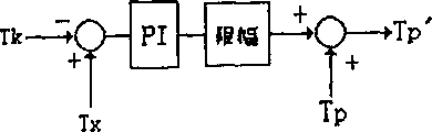
The synchronized algorithm controller as shown in Figure 6, it calculates Tx and Tk1 time difference Δ T=Tx-Tk1, proportion of utilization is regulated (P adjusting), proportional integral adjusting (PI adjusting) or other complicated adjusters are finely tuned the slave converter on timing cycle Tp basis carrier cycle Tp ', make Tp '=Tp+f (Δ T), utilize the slave switch carrier wave timing cycle in the synchronous governor fine adjustment parallel connection converter, realize the synchronous of slave switch and host switch with the method for sync carrier.The synchronized algorithm controller can require because the configuration of second timer is different to change to some extent.
Be example with the parallelly connected reverse converter system in the embodiment of the invention one, specify its course of work below.
As shown in Figure 7, two single-phase inverter parallel systems, DC bus-bar voltage are 2Vdc, and L, C are the inverter filter capacitor, and C1 is the bus filter capacitor, and K1 and K2 are two switches of inverter 1, and K1 ' and K2 ' are two switches of inverter 2.The slave switch periods lags behind main frame, in order to reduce two circulation between the inverter, needs control switch K1 and K1 ', and K2 and K2 ' keep keeping strokes.
Be depicted as K1 and K1 ' as Fig. 8 a, the situation that K2 and K2 ' keep strokes, two inverters whiles of this moment do not have high-frequency current each other to the load energy supply; Be depicted as K1 and K1 ' as Fig. 8 b, K2 and K2 ' move inconsistent situation, and have the pressure drop of 2Vdc this moment between two filter inductances, must cause that bigger high frequency circulation is arranged between two inverters.
In the present embodiment, first timer in each inverter is simultaneously as switch carrier wave timer, if realized every inverter first timer in the parallelly connected reverse converter system synchronously, also just can realize the synchronous of switch.
In the parallelly connected reverse converter system, every inverter first timer is set at rising/decline count mode, and the count cycle is Tp, and second timer is set at dull rising count mode, and the count cycle is 2Tp.
1, synchronizing signal produces
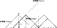
As shown in Figure 9, among the figure as 1 Timer1 that draws of inverter of main frame, and as the inverter 2 of slave drawn Timer1 and Timer2 (distinguishing with the actual situation line), and Timer1 and TImer2 count from zero simultaneously, and final purpose of the present invention is that realization main frame Timer1 and the next switch periods of slave Timer1 after Synchronization Control are carried out synchronously.
At first, the pulse transmitter in the main frame inverter sends lock-out pulse to synchronous bus with the fixed or changed cycle when the set time of first timer Tk1=Tp.
2, synchronizing signal receives
As shown in Figure 9, all slave inverter second timer cycles are 2Tp, all utilize acquisition equipment to catch lock-out pulse along information on synchronous bus, and write down the time state Tx=T1 of second timer in slave this moment.
3, slave is implemented synchronized algorithm
All slave inverters are implemented synchronized algorithm, adjust its switch carrier cycle, thereby realization is synchronous with host switch, and the detailed process of adjustment is as follows:
Tx and the difference Δ T of Tk1 writing time is caught in calculating
ΔT=Tx-Tk1=T1-Tp
Utilize P to be adjusted in regularly the carrier cycle Tp ' of fine setting slave inverter on the carrier wave timing cycle Tp basis, realize carrier synchronization, desirable proportional control factor Kp=0.5 in order to realize adjusted next switch periods:
Tp’=Tp+Kp*ΔT=TP+(T1-Tp)/2=(T1+Tp)/2
As can be seen from Figure 9, the slave first timer just can be realized synchronously in adjusted next switch periods, thereby realize the synchronous of switch carrier wave.
Be example with the parallel rectifier system in the embodiment of the invention two, specify its course of work below.
As shown in figure 10, two single-phase rectifier parallel systems, L1 and L2, L1 ' and L2 ' are respectively two rectifier inductance, and K1, K2, K3, K4 and K1 ', K2 ', K3 ', K4 ' are respectively two rectifier rectification device switches, and C is a filter capacitor.The slave switch periods lags behind main frame, in order to reduce two energy Flow between the rectifier, two rectifiers need be driven simultaneously to inductive switch.
In Figure 11 a, K1 and K1 ', K4 and K4 ' drive simultaneously, then do not have energy Flow between the rectifier; In Figure 11 b, K1 and K1 ', K4 and K4 ' are asynchronous, and then rectifier 1 inductance L 1 has energy Flow by K1 between K3 ' and rectifier 2 inductance L 2 ', promptly has circulation between two rectifiers.
In the present embodiment, every rectifier is switch carrier wave timer with the first timer, and controls constantly as main frame transmission lock-out pulse simultaneously, realizes that so every rectifier first timer just can be realized the synchronous of switch synchronously in the parallel rectifier system.
In the parallel rectifier system, every rectifier first timer is set at rising/decline count mode, and the count cycle is Tp, and second timer is set at dull count mode down, and the count cycle is 2Tp.
1, synchronizing signal produces
As shown in figure 12, among the figure as 1 Timer1 that draws of rectifier of main frame, and as the rectifier 2 of slave drawn Timer1 and Timer2, and Timer1 and TImer2 keep synchronously, the wherein Timer1 rising of starting from scratch, Timer2 descends since 2 * Tp, and final purpose is that realization main frame Timer1 and following two switch periods of slave Timer1 after Synchronization Control are carried out synchronously.
At first, the pulse transmitter in the main frame rectifier sends lock-out pulse with the fixed or changed cycle to synchronous bus at the set time of first timer Tk1=Tp.
2, synchronizing signal receives
As shown in figure 12, all slave rectifier second timer cycles are 2 * Tp, all utilize acquisition equipment to catch lock-out pulse along information on synchronous bus, and write down the time state Tx=T1 of second timer in slave this moment.
3, slave is implemented synchronized algorithm
All slave rectifiers are implemented synchronized algorithm, adjust its switch carrier cycle, thereby realization is synchronous with host switch, and the detailed process of adjustment is as follows:
Tx and the difference Δ T of Tk1 writing time is caught in calculating
ΔT=Tx-Tk1=T1-Tp
Utilize P to be adjusted in regularly the carrier cycle Tp ' that finely tunes the slave rectifier on the carrier wave timing cycle Tp basis, in order to realize adjusted following two switch periods carrier synchronization, desirable proportional control factor Kp=0.25:
Tp’=Tp+Kp*ΔT=TP+(Tp-T1)/4=(5*Tp-T1)/4
As can be seen from Figure 12, the slave first timer just can be realized synchronously in adjusted following two cycles, thereby realize the synchronous of switch carrier wave.
In the above embodiments, be provided with two timers simultaneously in each contrary parallel operation or the rectifier, in fact only establishing a timer in each converter also can realize synchronously, be example with parallelly connected reverse converter system shown in Figure 7 below, specify the course of work that each inverter of the present invention has only a timer, that is to say and have only a first timer in the main frame to have only second o'clock device in the slave.
First timer in the main frame inverter sends lock-out pulse by pulse transmitter and controls constantly, and simultaneously as host switch carrier wave timer; Second o'clock device in the slave is simultaneously as slave switch carrier wave timer.If realized the synchronous of slave inverter second timer and main frame inverter first timer, also just can realize the synchronous of switch.
Wherein, capture moment of pulse edge with second timer recording impulse acquisition equipment from synchronous bus in the slave inverter, the timer in every inverter all is set at dull rising count mode, and the count cycle is Tp (immobilizing).
1, synchronizing signal produces
As shown in figure 13, the pulse transmitter that is set as in the inverter 1 of main frame sends lock-out pulse with the fixed or changed cycle to synchronous bus at the set time of first timer Tk1=Tp.
2, synchronizing signal receives
As shown in figure 13, slave inverter 2 utilizes acquisition equipment to catch lock-out pulse along information on synchronous bus, and writes down the time state Tx=T1 of second timer in slave this moment.
3, slave is implemented synchronized algorithm
Tx and Tk1 poor writing time is caught in calculating
ΔT=Tx-Tk1=T1-Tp
Utilize P to be adjusted in regularly the carrier cycle Tp ' of fine setting slave inverter on the carrier wave timing cycle Tp basis, realize carrier synchronization, desirable proportional control factor Kp=1 in order to realize adjusted next switch periods:
Tp’=Tp+Kp*ΔT=TP+(T1-Tp)=T1
As can be seen from Figure 13, the slave second timer just can be realized synchronously in adjusted next switch periods, thereby realize the synchronous of switch carrier wave.
Method of the present invention is not limited to the above embodiments, for example in embodiment three, can also set up the switch carrier wave timer of a timer as this inverter in each inverter, the relation between first timer in the main frame inverter and the switch carrier wave timer, between the second timer in the slave inverter and the switch carrier wave timer is obeyed the first predetermined agreement.Wherein, described first agreement can be stipulated to keep between first timer in the main frame inverter and the switch carrier wave timer synchronously; Keep synchronously between second timer in the same slave inverter and the switch carrier wave timer.Switch carrier wave timer in also can regulation main frame inverter is leading or lag behind set time of first timer; Switch carrier wave timer in the same slave inverter is leading or lag behind set time of second timer.
Claims (10)
1, a kind of switch synchronization method of parallel converter system, it is characterized in that, one of them converter is made as main frame, all the other converters all are made as slave, be provided with a first timer and a pulse transmitter in the described main frame converter, be provided with a second timer, a pulse edge acquisition equipment and a synchronous governor in the described slave converter, it is synchronous that described changer system carries out switch according to the following steps:
First timer in the main frame converter sends lock-out pulse at a fixed time Tk1 by described pulse transmitter on synchronous bus;
Described second timer in the slave converter writes down described acquisition equipment receives described lock-out pulse edge from synchronous bus moment Tx;
Described synchronous governor is implemented synchronized algorithm according to described Tk1 and Tx, regulate second timer in the slave converter make it with the main frame converter in first timer synchronous, press predetermined protocol then and regulate switch carrier wave timer in the slave converter, make it with the main frame converter in switch carrier wave timer synchronous.
2, method according to claim 1 is characterized in that, the first timer while in the described main frame converter is as the switch carrier wave timer of this converter; The second timer while in the slave converter is as the switch carrier wave timer of this converter.
3, method according to claim 1, it is characterized in that, in each converter, also be provided with the switch carrier wave timer of a timer as this converter, the relation between first timer in the main frame converter and the switch carrier wave timer, between the second timer in the slave converter and the switch carrier wave timer is obeyed the first predetermined agreement.
4, method according to claim 3 is characterized in that, keeps synchronously between first timer in described first agreement regulation main frame converter and the switch carrier wave timer; Keep synchronously between second timer in the same slave converter and the switch carrier wave timer.
5, method according to claim 3 is characterized in that, the switch carrier wave timer in the described first agreement regulation main frame converter is leading or lag behind set time of first timer; Switch carrier wave timer in the same slave converter is leading or lag behind set time of second timer.
6, method according to claim 1 is characterized in that, sets up a second timer in described main frame converter, sets up a first timer simultaneously in described slave converter; First timer in the same converter and second timer keep synchronously, and relation is between the two obeyed the second predetermined agreement.
7, method according to claim 6, it is characterized in that, the described second agreement regulation is configured to dull count mode with second timer, if the first timer in the same converter is configured to rising/decline count mode, then the cycle of second timer is 2 times of first timer cycle; If the first timer in the same converter is configured to dull the rising or dull decline count mode, then the cycle of second timer is identical with the cycle of first timer.
8, method according to claim 6 is characterized in that, the first timer while in each converter is as the switch carrier wave timer of this converter.
9, according to each described method in the claim 1 to 8, it is characterized in that described synchronized algorithm is: Tp '=Tp+Kp* Δ T, Tp is described carrier wave timer cycle, Tp ' is the carrier wave timer cycle after finely tuning, and Δ T=Tx-Tk1, Kp are proportional control factors.
According to any one described method among the claim 1-8, it is characterized in that 10, described synchronous governor is that proportional integral is regulated or ratio is regulated.
Priority Applications (5)
| Application Number | Priority Date | Filing Date | Title |
|---|---|---|---|
| CNB011301783A CN1228908C (en) | 2001-12-31 | 2001-12-31 | Switch synchronization method of parallel converter system. |
| US10/335,231 US6788559B2 (en) | 2001-12-31 | 2002-12-30 | Method of switching synchronization of parallel-connected converter system |
| EP02029082A EP1324480B1 (en) | 2001-12-31 | 2002-12-30 | Method of switching synchronization of parallel-connected converter system |
| AT02029082T ATE338372T1 (en) | 2001-12-31 | 2002-12-30 | METHOD FOR CLOCK SYNCHRONIZING A SYSTEM WITH PARALLEL-CONNECTED CONVERTERS |
| DE60214327T DE60214327D1 (en) | 2001-12-31 | 2002-12-30 | Method for clock synchronization of a system with parallel-connected converters |
Applications Claiming Priority (1)
| Application Number | Priority Date | Filing Date | Title |
|---|---|---|---|
| CNB011301783A CN1228908C (en) | 2001-12-31 | 2001-12-31 | Switch synchronization method of parallel converter system. |
Publications (2)
| Publication Number | Publication Date |
|---|---|
| CN1430325A CN1430325A (en) | 2003-07-16 |
| CN1228908C true CN1228908C (en) | 2005-11-23 |
Family
ID=4669802
Family Applications (1)
| Application Number | Title | Priority Date | Filing Date |
|---|---|---|---|
| CNB011301783A Expired - Lifetime CN1228908C (en) | 2001-12-31 | 2001-12-31 | Switch synchronization method of parallel converter system. |
Country Status (5)
| Country | Link |
|---|---|
| US (1) | US6788559B2 (en) |
| EP (1) | EP1324480B1 (en) |
| CN (1) | CN1228908C (en) |
| AT (1) | ATE338372T1 (en) |
| DE (1) | DE60214327D1 (en) |
Cited By (1)
| Publication number | Priority date | Publication date | Assignee | Title |
|---|---|---|---|---|
| CN111327194A (en) * | 2018-12-13 | 2020-06-23 | 台达电子工业股份有限公司 | Power converter and power supply device sharing direct-current power supply |
Families Citing this family (45)
| Publication number | Priority date | Publication date | Assignee | Title |
|---|---|---|---|---|
| SE0102230L (en) * | 2001-06-25 | 2002-12-26 | Ragnar Joensson | Switching circuit with multiple steps |
| CN1215636C (en) * | 2001-12-31 | 2005-08-17 | 艾默生网络能源有限公司 | Method of establishing host machine in multi-module parallel system |
| US7596699B2 (en) * | 2004-02-24 | 2009-09-29 | Intersil Americas Inc. | Battery authentication system |
| US7729427B2 (en) * | 2004-02-24 | 2010-06-01 | Intersil Americas Inc. | Pseudo-synchronous one wire bidirectional bus interface |
| US7142140B2 (en) | 2004-07-27 | 2006-11-28 | Silicon Laboratories Inc. | Auto scanning ADC for DPWM |
| US7446430B2 (en) * | 2005-03-31 | 2008-11-04 | Silicon Laboratories Inc. | Plural load distributed power supply system with shared master for controlling remote digital DC/DC converters |
| US7518894B2 (en) * | 2005-03-31 | 2009-04-14 | Silicon Laboratories Inc. | Distributed power supply system having reassignable master |
| FI118875B (en) * | 2006-09-26 | 2008-04-15 | Vacon Oyj | Parallel connection of inverters |
| CN101154093B (en) * | 2006-09-26 | 2011-06-15 | 力博特公司 | Method and apparatus for competing for host computer position in parallel system |
| US7593243B2 (en) * | 2006-10-09 | 2009-09-22 | Honeywell International Inc. | Intelligent method for DC bus voltage ripple compensation for power conversion units |
| US7420498B2 (en) * | 2006-11-22 | 2008-09-02 | Infineon Technologies Ag | Signal converter performing a role |
| GB2444528B (en) * | 2006-12-09 | 2011-07-06 | Converteam Ltd | Methods for synchronising a plurality of generators |
| CN101494383B (en) * | 2008-01-23 | 2011-12-14 | 力博特公司 | Control method for parallel connection system of inverter |
| EP2449660B1 (en) * | 2009-06-30 | 2019-03-27 | Saab AB | Method for reducing electromagnetic interference radiated from a power supply arrangement |
| EP2270970B1 (en) * | 2009-07-02 | 2012-04-04 | Converteam Technology Ltd | Control methods for the synchronisation of parallel-connected power converters operating in accordance with a pulse width modulation (PWM) strategy |
| EP2489116B1 (en) * | 2009-10-14 | 2018-07-25 | ABB Research Ltd. | Wireless control of power network switching devices |
| DE102010003614A1 (en) | 2010-04-01 | 2011-10-06 | Robert Bosch Gmbh | Circuit arrangement with at least two parallel-connected inverter modules, method for parallel connection of at least two inverter modules and circuit carrier for a gate drive circuit of an inverter module |
| JP5656571B2 (en) * | 2010-11-09 | 2015-01-21 | 株式会社ケーヒン | Communications system |
| CN102468766A (en) * | 2010-11-10 | 2012-05-23 | 永济新时速电机电器有限责任公司 | Combined frequency converter |
| CN102075072B (en) * | 2010-11-19 | 2013-03-20 | 国网电力科学研究院武汉南瑞有限责任公司 | Staggered parallel high-stability modularized direct-current current-stabilized power supply system and staggered parallel connection method thereof |
| US8120935B2 (en) * | 2011-03-29 | 2012-02-21 | American Superconductor Corporation | Power converter with dual ring network control |
| KR101304055B1 (en) * | 2012-06-18 | 2013-09-04 | 미쓰비시덴키 가부시키가이샤 | Inverter system and communication method |
| DE102013002114A1 (en) * | 2013-02-08 | 2014-08-14 | B2 Electronic Gmbh | Mobile high voltage tester |
| CN103997069B (en) * | 2013-02-18 | 2015-12-02 | 力博特公司 | UPS parallel system and counter synchronization signal method of reseptance thereof |
| WO2015050092A1 (en) * | 2013-10-02 | 2015-04-09 | 株式会社村田製作所 | Power supply system |
| JP5999271B2 (en) * | 2013-10-02 | 2016-09-28 | 株式会社村田製作所 | Power supply system and power supply unit |
| EP2897268B1 (en) | 2014-01-20 | 2022-01-05 | ABB Schweiz AG | Master/slave controller system in ring topology for modular multilevel converters |
| JP6358859B2 (en) * | 2014-06-04 | 2018-07-18 | 東芝機械株式会社 | Inverter power generation system and inverter power generation device |
| CN104503523B (en) * | 2014-10-31 | 2016-06-15 | 广东易事特电源股份有限公司 | UPS Parallel opertation system and main frame therein and from machine, UPS Parallel opertation voltage control method and device |
| CN105656338B (en) * | 2014-11-14 | 2018-08-14 | 比亚迪股份有限公司 | The common-mode voltage suppressing method and inverter system of multiple inverters |
| US10654682B2 (en) | 2014-12-17 | 2020-05-19 | Otis Elevator Company | Conveyance system having paralleled drives |
| CN104486059B (en) * | 2015-01-04 | 2018-07-03 | 阳光电源股份有限公司 | A kind of photovoltaic DC-to-AC converter parallel system carrier synchronization method and device |
| CN106374550A (en) * | 2015-07-24 | 2017-02-01 | 比亚迪股份有限公司 | Electric vehicle charging system and charging control method thereof |
| US10833603B2 (en) | 2017-01-30 | 2020-11-10 | Carrier Corporation | Method of controlling paralleled passive front-end rectifiers with and without inter-leaving |
| EP3574579B1 (en) | 2017-01-30 | 2023-11-08 | Carrier Corporation | Paralleled passive front-end rectifiers with and without interleaving |
| JP6717239B2 (en) * | 2017-03-07 | 2020-07-01 | トヨタ自動車株式会社 | Boost converter device |
| FR3070228B1 (en) * | 2017-08-18 | 2019-09-13 | Alstom Transport Technologies | POWER CONVERTER IN BROADBAND SEMICONDUCTOR TECHNOLOGY PROHIBITED |
| JP6922576B2 (en) * | 2017-09-13 | 2021-08-18 | 株式会社明電舎 | Synchronous control method of inverter system and inverter system |
| CN107948108A (en) * | 2017-11-17 | 2018-04-20 | 厦门科华恒盛股份有限公司 | A kind of DSP devices carrier synchronization method and system |
| CN108206623B (en) * | 2017-12-08 | 2020-03-20 | 南京南瑞继保电气有限公司 | Carrier synchronization system and method for parallel connection of converters |
| EP3703241B1 (en) * | 2019-02-26 | 2022-07-13 | Hitachi Energy Switzerland AG | Communication in a converter device |
| CN110971557B (en) * | 2019-11-26 | 2023-05-26 | 阳光电源股份有限公司 | Carrier synchronization method and system for parallel operation of multiple converters |
| CN111628571B (en) * | 2020-04-29 | 2022-03-11 | 科华恒盛股份有限公司 | Master-slave-free carrier synchronization method for multi-module system and multi-module carrier synchronization system |
| CN114257074B (en) * | 2021-12-15 | 2024-03-08 | 中车长春轨道客车股份有限公司 | Inverter parallel switch circulation suppression algorithm based on carrier phase synchronization |
| CN116455545B (en) * | 2023-06-16 | 2023-09-12 | 惠州市乐亿通科技有限公司 | Signal synchronization method, device and system |
Family Cites Families (9)
| Publication number | Priority date | Publication date | Assignee | Title |
|---|---|---|---|---|
| IT1185262B (en) * | 1985-07-16 | 1987-11-04 | Italtel Spa | CIRCUIT PROVISION FOR THE SYNCHRONIZATION OF A POWER SUPPLY UNIT COMPLEX |
| US5193054A (en) | 1991-10-24 | 1993-03-09 | Sundstrand Corporation | DC content control in a dual VSCF converter system |
| US5907482A (en) * | 1995-11-30 | 1999-05-25 | Toko, Inc. | Power supply control device |
| US5684684A (en) * | 1996-04-29 | 1997-11-04 | Natel Engineering Company, Inc. | DC or capacitively coupled bi-directional sync |
| US5808453A (en) * | 1996-08-21 | 1998-09-15 | Siliconix Incorporated | Synchronous current sharing pulse width modulator |
| DE10060429A1 (en) | 1999-12-16 | 2001-07-12 | Caterpillar Inc | Power transmitter; has control circuit to transmit n instruction signals to n power converter circuits, which are driven to transfer n pulse width modulated signals out of phase by 360/n degrees |
| DE10003730A1 (en) | 2000-01-28 | 2001-08-02 | Bosch Gmbh Robert | Method and device for regulating the parallel operation of DC-DC converters |
| US6169679B1 (en) | 2000-03-21 | 2001-01-02 | Ford Motor Company | Method and system for synchronizing the phase angles of parallel connected inverters |
| FR2820923B1 (en) | 2001-02-09 | 2003-06-13 | Atmel Nantes Sa | POWER SUPPLY FOR SERIAL LINK, SLAVE MASTER TYPE |
-
2001
- 2001-12-31 CN CNB011301783A patent/CN1228908C/en not_active Expired - Lifetime
-
2002
- 2002-12-30 DE DE60214327T patent/DE60214327D1/en not_active Expired - Lifetime
- 2002-12-30 US US10/335,231 patent/US6788559B2/en not_active Expired - Fee Related
- 2002-12-30 EP EP02029082A patent/EP1324480B1/en not_active Expired - Lifetime
- 2002-12-30 AT AT02029082T patent/ATE338372T1/en not_active IP Right Cessation
Cited By (2)
| Publication number | Priority date | Publication date | Assignee | Title |
|---|---|---|---|---|
| CN111327194A (en) * | 2018-12-13 | 2020-06-23 | 台达电子工业股份有限公司 | Power converter and power supply device sharing direct-current power supply |
| CN111327194B (en) * | 2018-12-13 | 2021-08-06 | 台达电子工业股份有限公司 | Power converter and power supply device sharing direct-current power supply |
Also Published As
| Publication number | Publication date |
|---|---|
| DE60214327D1 (en) | 2006-10-12 |
| US6788559B2 (en) | 2004-09-07 |
| CN1430325A (en) | 2003-07-16 |
| US20030137856A1 (en) | 2003-07-24 |
| EP1324480A2 (en) | 2003-07-02 |
| ATE338372T1 (en) | 2006-09-15 |
| EP1324480B1 (en) | 2006-08-30 |
| EP1324480A3 (en) | 2004-09-01 |
Similar Documents
| Publication | Publication Date | Title |
|---|---|---|
| CN1228908C (en) | Switch synchronization method of parallel converter system. | |
| CN1246954C (en) | Switch type power source | |
| CN1262384C (en) | Arc component processing power source with component for reducing switch loss | |
| CN1258258C (en) | Electric motor speed and direction controller and method | |
| CN1039158A (en) | Uninterrupted power supply(ups) | |
| CN1663728A (en) | Soft-switching half-bridge inverter power supply system | |
| CN101039081A (en) | Apparatus and method for supplying DC power source | |
| CN1822479A (en) | Pwm controller with dual-edge modulation using dual ramps | |
| CN1825743A (en) | LLC series resonant converter and its synchronous rectifying power switch driving method | |
| CN102088266A (en) | Brushless motor stepless speed change controller based on FPGA (Field Programmable Gate Array) digitization control | |
| CN1780131A (en) | Pulse width modulator with automatic change of outputting frequency | |
| CN111193391B (en) | Staggered parallel totem-pole bridgeless PFC phase control method | |
| CN1666404A (en) | Dc-dc converter | |
| CN201967167U (en) | Induction heating dual-cycle controller | |
| CN1898853A (en) | Switched mode power supply | |
| CN1533018A (en) | Integration converton with three phase power factor correction | |
| CN2590271Y (en) | Electric power unit | |
| CN2489367Y (en) | AC switch compensating voltage stabilizer | |
| CN106329957A (en) | Electric tool and control method thereof | |
| CN1228907C (en) | Semi-bridge type PFC bus voltage eqaulation control method and device | |
| CN201904749U (en) | FPGA (field programmable gate array) digital control based variable speed controller for brushless motor | |
| CN1767368A (en) | Method and apparatus for controlling AC induction motor energy-saving operation | |
| CN1285168C (en) | Controller for inverter device | |
| CN1485543A (en) | UPS fan controlling method | |
| CN204334408U (en) | The adjustable-speed motor of adjustable-speed motor performance optimization device and performance optimization |
Legal Events
| Date | Code | Title | Description |
|---|---|---|---|
| C06 | Publication | ||
| PB01 | Publication | ||
| C10 | Entry into substantive examination | ||
| SE01 | Entry into force of request for substantive examination | ||
| C14 | Grant of patent or utility model | ||
| GR01 | Patent grant | ||
| CP03 | Change of name, title or address |
Address after: Nanshan District Xueyuan Road in Shenzhen city of Guangdong province 518055 No. 1001 Nanshan Chi Park B2 building 1-4 floor, building 6-10 Patentee after: Vitamin Technology Co., Ltd. Address before: 518057 Nanshan District science and Technology Industrial Park, Guangdong, Shenzhen Branch Road, No. Patentee before: Aimosheng Network Energy Source Co., Ltd. |
|
| CP03 | Change of name, title or address | ||
| CX01 | Expiry of patent term |
Granted publication date: 20051123 |
|
| CX01 | Expiry of patent term |