CN1227733C - Semiconductor device - Google Patents
Semiconductor device Download PDFInfo
- Publication number
- CN1227733C CN1227733C CNB011258381A CN01125838A CN1227733C CN 1227733 C CN1227733 C CN 1227733C CN B011258381 A CNB011258381 A CN B011258381A CN 01125838 A CN01125838 A CN 01125838A CN 1227733 C CN1227733 C CN 1227733C
- Authority
- CN
- China
- Prior art keywords
- unit amplifier
- amplifier
- earth connection
- semiconductor device
- pin
- Prior art date
- Legal status (The legal status is an assumption and is not a legal conclusion. Google has not performed a legal analysis and makes no representation as to the accuracy of the status listed.)
- Expired - Fee Related
Links
Images


Classifications
-
- H—ELECTRICITY
- H04—ELECTRIC COMMUNICATION TECHNIQUE
- H04B—TRANSMISSION
- H04B1/00—Details of transmission systems, not covered by a single one of groups H04B3/00 - H04B13/00; Details of transmission systems not characterised by the medium used for transmission
- H04B1/005—Details of transmission systems, not covered by a single one of groups H04B3/00 - H04B13/00; Details of transmission systems not characterised by the medium used for transmission adapting radio receivers, transmitters andtransceivers for operation on two or more bands, i.e. frequency ranges
- H04B1/0053—Details of transmission systems, not covered by a single one of groups H04B3/00 - H04B13/00; Details of transmission systems not characterised by the medium used for transmission adapting radio receivers, transmitters andtransceivers for operation on two or more bands, i.e. frequency ranges with common antenna for more than one band
- H04B1/006—Details of transmission systems, not covered by a single one of groups H04B3/00 - H04B13/00; Details of transmission systems not characterised by the medium used for transmission adapting radio receivers, transmitters andtransceivers for operation on two or more bands, i.e. frequency ranges with common antenna for more than one band using switches for selecting the desired band
-
- H—ELECTRICITY
- H03—ELECTRONIC CIRCUITRY
- H03F—AMPLIFIERS
- H03F3/00—Amplifiers with only discharge tubes or only semiconductor devices as amplifying elements
- H03F3/45—Differential amplifiers
-
- H—ELECTRICITY
- H01—ELECTRIC ELEMENTS
- H01L—SEMICONDUCTOR DEVICES NOT COVERED BY CLASS H10
- H01L23/00—Details of semiconductor or other solid state devices
- H01L23/48—Arrangements for conducting electric current to or from the solid state body in operation, e.g. leads, terminal arrangements ; Selection of materials therefor
- H01L23/50—Arrangements for conducting electric current to or from the solid state body in operation, e.g. leads, terminal arrangements ; Selection of materials therefor for integrated circuit devices, e.g. power bus, number of leads
-
- H—ELECTRICITY
- H01—ELECTRIC ELEMENTS
- H01L—SEMICONDUCTOR DEVICES NOT COVERED BY CLASS H10
- H01L23/00—Details of semiconductor or other solid state devices
- H01L23/58—Structural electrical arrangements for semiconductor devices not otherwise provided for, e.g. in combination with batteries
- H01L23/64—Impedance arrangements
- H01L23/66—High-frequency adaptations
-
- H—ELECTRICITY
- H04—ELECTRIC COMMUNICATION TECHNIQUE
- H04B—TRANSMISSION
- H04B1/00—Details of transmission systems, not covered by a single one of groups H04B3/00 - H04B13/00; Details of transmission systems not characterised by the medium used for transmission
- H04B1/005—Details of transmission systems, not covered by a single one of groups H04B3/00 - H04B13/00; Details of transmission systems not characterised by the medium used for transmission adapting radio receivers, transmitters andtransceivers for operation on two or more bands, i.e. frequency ranges
-
- H—ELECTRICITY
- H04—ELECTRIC COMMUNICATION TECHNIQUE
- H04B—TRANSMISSION
- H04B1/00—Details of transmission systems, not covered by a single one of groups H04B3/00 - H04B13/00; Details of transmission systems not characterised by the medium used for transmission
- H04B1/06—Receivers
- H04B1/16—Circuits
- H04B1/26—Circuits for superheterodyne receivers
- H04B1/28—Circuits for superheterodyne receivers the receiver comprising at least one semiconductor device having three or more electrodes
-
- H—ELECTRICITY
- H01—ELECTRIC ELEMENTS
- H01L—SEMICONDUCTOR DEVICES NOT COVERED BY CLASS H10
- H01L2223/00—Details relating to semiconductor or other solid state devices covered by the group H01L23/00
- H01L2223/58—Structural electrical arrangements for semiconductor devices not otherwise provided for
- H01L2223/64—Impedance arrangements
- H01L2223/66—High-frequency adaptations
- H01L2223/6605—High-frequency electrical connections
- H01L2223/6611—Wire connections
-
- H—ELECTRICITY
- H01—ELECTRIC ELEMENTS
- H01L—SEMICONDUCTOR DEVICES NOT COVERED BY CLASS H10
- H01L2223/00—Details relating to semiconductor or other solid state devices covered by the group H01L23/00
- H01L2223/58—Structural electrical arrangements for semiconductor devices not otherwise provided for
- H01L2223/64—Impedance arrangements
- H01L2223/66—High-frequency adaptations
- H01L2223/6644—Packaging aspects of high-frequency amplifiers
-
- H—ELECTRICITY
- H01—ELECTRIC ELEMENTS
- H01L—SEMICONDUCTOR DEVICES NOT COVERED BY CLASS H10
- H01L2224/00—Indexing scheme for arrangements for connecting or disconnecting semiconductor or solid-state bodies and methods related thereto as covered by H01L24/00
- H01L2224/01—Means for bonding being attached to, or being formed on, the surface to be connected, e.g. chip-to-package, die-attach, "first-level" interconnects; Manufacturing methods related thereto
- H01L2224/02—Bonding areas; Manufacturing methods related thereto
- H01L2224/04—Structure, shape, material or disposition of the bonding areas prior to the connecting process
- H01L2224/05—Structure, shape, material or disposition of the bonding areas prior to the connecting process of an individual bonding area
- H01L2224/0554—External layer
- H01L2224/05599—Material
-
- H—ELECTRICITY
- H01—ELECTRIC ELEMENTS
- H01L—SEMICONDUCTOR DEVICES NOT COVERED BY CLASS H10
- H01L2224/00—Indexing scheme for arrangements for connecting or disconnecting semiconductor or solid-state bodies and methods related thereto as covered by H01L24/00
- H01L2224/01—Means for bonding being attached to, or being formed on, the surface to be connected, e.g. chip-to-package, die-attach, "first-level" interconnects; Manufacturing methods related thereto
- H01L2224/42—Wire connectors; Manufacturing methods related thereto
- H01L2224/44—Structure, shape, material or disposition of the wire connectors prior to the connecting process
- H01L2224/45—Structure, shape, material or disposition of the wire connectors prior to the connecting process of an individual wire connector
- H01L2224/45001—Core members of the connector
- H01L2224/45099—Material
-
- H—ELECTRICITY
- H01—ELECTRIC ELEMENTS
- H01L—SEMICONDUCTOR DEVICES NOT COVERED BY CLASS H10
- H01L2224/00—Indexing scheme for arrangements for connecting or disconnecting semiconductor or solid-state bodies and methods related thereto as covered by H01L24/00
- H01L2224/01—Means for bonding being attached to, or being formed on, the surface to be connected, e.g. chip-to-package, die-attach, "first-level" interconnects; Manufacturing methods related thereto
- H01L2224/42—Wire connectors; Manufacturing methods related thereto
- H01L2224/47—Structure, shape, material or disposition of the wire connectors after the connecting process
- H01L2224/48—Structure, shape, material or disposition of the wire connectors after the connecting process of an individual wire connector
- H01L2224/481—Disposition
- H01L2224/48151—Connecting between a semiconductor or solid-state body and an item not being a semiconductor or solid-state body, e.g. chip-to-substrate, chip-to-passive
- H01L2224/48221—Connecting between a semiconductor or solid-state body and an item not being a semiconductor or solid-state body, e.g. chip-to-substrate, chip-to-passive the body and the item being stacked
- H01L2224/48245—Connecting between a semiconductor or solid-state body and an item not being a semiconductor or solid-state body, e.g. chip-to-substrate, chip-to-passive the body and the item being stacked the item being metallic
- H01L2224/48247—Connecting between a semiconductor or solid-state body and an item not being a semiconductor or solid-state body, e.g. chip-to-substrate, chip-to-passive the body and the item being stacked the item being metallic connecting the wire to a bond pad of the item
-
- H—ELECTRICITY
- H01—ELECTRIC ELEMENTS
- H01L—SEMICONDUCTOR DEVICES NOT COVERED BY CLASS H10
- H01L2224/00—Indexing scheme for arrangements for connecting or disconnecting semiconductor or solid-state bodies and methods related thereto as covered by H01L24/00
- H01L2224/01—Means for bonding being attached to, or being formed on, the surface to be connected, e.g. chip-to-package, die-attach, "first-level" interconnects; Manufacturing methods related thereto
- H01L2224/42—Wire connectors; Manufacturing methods related thereto
- H01L2224/47—Structure, shape, material or disposition of the wire connectors after the connecting process
- H01L2224/49—Structure, shape, material or disposition of the wire connectors after the connecting process of a plurality of wire connectors
- H01L2224/491—Disposition
- H01L2224/4912—Layout
- H01L2224/49171—Fan-out arrangements
-
- H—ELECTRICITY
- H01—ELECTRIC ELEMENTS
- H01L—SEMICONDUCTOR DEVICES NOT COVERED BY CLASS H10
- H01L2224/00—Indexing scheme for arrangements for connecting or disconnecting semiconductor or solid-state bodies and methods related thereto as covered by H01L24/00
- H01L2224/80—Methods for connecting semiconductor or other solid state bodies using means for bonding being attached to, or being formed on, the surface to be connected
- H01L2224/85—Methods for connecting semiconductor or other solid state bodies using means for bonding being attached to, or being formed on, the surface to be connected using a wire connector
- H01L2224/8538—Bonding interfaces outside the semiconductor or solid-state body
- H01L2224/85399—Material
-
- H—ELECTRICITY
- H01—ELECTRIC ELEMENTS
- H01L—SEMICONDUCTOR DEVICES NOT COVERED BY CLASS H10
- H01L24/00—Arrangements for connecting or disconnecting semiconductor or solid-state bodies; Methods or apparatus related thereto
- H01L24/01—Means for bonding being attached to, or being formed on, the surface to be connected, e.g. chip-to-package, die-attach, "first-level" interconnects; Manufacturing methods related thereto
- H01L24/42—Wire connectors; Manufacturing methods related thereto
- H01L24/47—Structure, shape, material or disposition of the wire connectors after the connecting process
- H01L24/48—Structure, shape, material or disposition of the wire connectors after the connecting process of an individual wire connector
-
- H—ELECTRICITY
- H01—ELECTRIC ELEMENTS
- H01L—SEMICONDUCTOR DEVICES NOT COVERED BY CLASS H10
- H01L24/00—Arrangements for connecting or disconnecting semiconductor or solid-state bodies; Methods or apparatus related thereto
- H01L24/01—Means for bonding being attached to, or being formed on, the surface to be connected, e.g. chip-to-package, die-attach, "first-level" interconnects; Manufacturing methods related thereto
- H01L24/42—Wire connectors; Manufacturing methods related thereto
- H01L24/47—Structure, shape, material or disposition of the wire connectors after the connecting process
- H01L24/49—Structure, shape, material or disposition of the wire connectors after the connecting process of a plurality of wire connectors
-
- H—ELECTRICITY
- H01—ELECTRIC ELEMENTS
- H01L—SEMICONDUCTOR DEVICES NOT COVERED BY CLASS H10
- H01L2924/00—Indexing scheme for arrangements or methods for connecting or disconnecting semiconductor or solid-state bodies as covered by H01L24/00
- H01L2924/0001—Technical content checked by a classifier
- H01L2924/00014—Technical content checked by a classifier the subject-matter covered by the group, the symbol of which is combined with the symbol of this group, being disclosed without further technical details
-
- H—ELECTRICITY
- H01—ELECTRIC ELEMENTS
- H01L—SEMICONDUCTOR DEVICES NOT COVERED BY CLASS H10
- H01L2924/00—Indexing scheme for arrangements or methods for connecting or disconnecting semiconductor or solid-state bodies as covered by H01L24/00
- H01L2924/01—Chemical elements
- H01L2924/01019—Potassium [K]
-
- H—ELECTRICITY
- H01—ELECTRIC ELEMENTS
- H01L—SEMICONDUCTOR DEVICES NOT COVERED BY CLASS H10
- H01L2924/00—Indexing scheme for arrangements or methods for connecting or disconnecting semiconductor or solid-state bodies as covered by H01L24/00
- H01L2924/10—Details of semiconductor or other solid state devices to be connected
- H01L2924/11—Device type
- H01L2924/13—Discrete devices, e.g. 3 terminal devices
- H01L2924/1304—Transistor
- H01L2924/1305—Bipolar Junction Transistor [BJT]
-
- H—ELECTRICITY
- H01—ELECTRIC ELEMENTS
- H01L—SEMICONDUCTOR DEVICES NOT COVERED BY CLASS H10
- H01L2924/00—Indexing scheme for arrangements or methods for connecting or disconnecting semiconductor or solid-state bodies as covered by H01L24/00
- H01L2924/10—Details of semiconductor or other solid state devices to be connected
- H01L2924/11—Device type
- H01L2924/14—Integrated circuits
-
- H—ELECTRICITY
- H01—ELECTRIC ELEMENTS
- H01L—SEMICONDUCTOR DEVICES NOT COVERED BY CLASS H10
- H01L2924/00—Indexing scheme for arrangements or methods for connecting or disconnecting semiconductor or solid-state bodies as covered by H01L24/00
- H01L2924/30—Technical effects
- H01L2924/301—Electrical effects
- H01L2924/30107—Inductance
-
- H—ELECTRICITY
- H01—ELECTRIC ELEMENTS
- H01L—SEMICONDUCTOR DEVICES NOT COVERED BY CLASS H10
- H01L2924/00—Indexing scheme for arrangements or methods for connecting or disconnecting semiconductor or solid-state bodies as covered by H01L24/00
- H01L2924/30—Technical effects
- H01L2924/301—Electrical effects
- H01L2924/3011—Impedance
- H01L2924/30111—Impedance matching
Abstract
In a differential low-noise amplifier built in a semiconductor integrated circuit for a dual-band wireless transceiver, impedance components of wire bonding and package that occur in emitters are reduced and a gain is improved. Ground pins of amplifiers of the differential amplifier forming a pair are arranged adjacent to each other. Input pins and ground pins of the same amplifier are arranged adjacent to each other. Signals of the adjacent pins are allowed to have inverse phases, and trans-coupling between the pins is utilized so as to reduce impedance of the transistor emitters.
Description
Technical field
The present invention relates to a kind of transceiver semiconductor device that is mainly used in radio communication.
Background of invention
The double frequency-band wireless receiving and dispatching of adorning differential low noise amplifier in Fig. 5 represents to use is with the configuration example of the terminal equipment of semiconductor integrated circuit (below, be called transceiver IC).
Transceiver IC501 is combination double frequency-band HFS circuit and a frequency-conversion circuit, and in be loaded on an integrated circuit on the chip.This IC is connected with the baseband I C515 of back level.Baseband I C carries out A/D, D/A conversion to signal, and carries out Digital Signal Processing.The transceiver part of transceiver IC501 is made of the differential low noise amplifier 502a of low-frequency band, low-frequency band receiving mixer 503a and the differential low noise amplifier 502b of high frequency band, high frequency band receiving mixer 503b, low pass filter 504, variable gain amplifier 505, modulator 507 and adjustment deviation PLL508.And, supply with the high-frequency local oscillation signal that frequency translation needs by high frequency synthesizer 509 and local oscillator 510 in addition, driver 511.Equally, supply with the low frequency local oscillation signal by low frequency synthesizer 512, local oscillator 513, driver 514.By low noise amplifier is made difference structure, with regard to the differential conversion of list that does not need to use tyre member transformer to carry out.Therefore, can reduce the number of member in addition.
Differential low noise amplifier is made of two Unit Amplifier with same structure, and 2 high-frequency signals that input phase is anti-phase also carry out differential amplification.
In adorn the example of the transceiver IC of differential low noise amplifier, there is Infinon company to be published in ISSCC2000, " the A RF Transceiver forDigital Wireless Communication in a 25GHz Si Bipolar Technology " in pp.144~145 and 451. according to paper is transceiver IC to DECT (Digital Enhanced CordlessTelecommunication).The low noise amplifier of receiving system is a difference structure, but holding wire and ground wire, pin configuration are all unclear.And, use be encapsulated as the TSSOP38 pin.
As the typical example that only makes differential amplifier ICization, IF band gain control amplifier, the TDA801IT (with reference to DATA SHEET, February, 1995) of the satellite television receiver of Philip (Philips) company arranged.Pin configuration shown in Fig. 7 and circuit block diagram.Circuit is a difference structure, by package pins IFI1 and IFI2 input, and from IFO1 and IFO2 output.Grounding leg is 1 pin.As another example, 1.6GHz frequency range differential-type wide-band amplifier, the μ PC2726T of NEC (day is electric) company arranged.Pin configuration shown in Fig. 8 and circuit diagram.Send out the in2 input from in1 exactly, from the integrated circuit shown in out1 and the out2.
But, have the differential amplifier of grounding leg in the Unit Amplifier of each differential amplifier, except that above-mentioned company, again can not find other IC manufacturers.
Summary of the invention
The objective of the invention is to improve the amplifier gain of differential structures such as low noise amplifier.
According to the present invention, a kind of semiconductor device, have semiconductor circuit chip, a plurality of terminal pins that are connected with this semiconductor circuit chip, reach the encapsulation that seals this semiconductor circuit chip, form 2 Unit Amplifier on the above-mentioned semiconductor circuit chip, these 2 Unit Amplifier form 1 differential amplifier, and this semiconductor device comprises: at least 2 earth connections that connect the 1st Unit Amplifier of above-mentioned 2 Unit Amplifier in the above-mentioned a plurality of leads pin; And at least 2 earth connections that connect the 2nd Unit Amplifier of above-mentioned 2 Unit Amplifier in the above-mentioned a plurality of leads pin, wherein, each the terminal pin disposed adjacent of each terminal pin and the earth connection that is connected above-mentioned the 2nd Unit Amplifier that connects the earth connection of above-mentioned the 1st Unit Amplifier.
According to the present invention, a kind of semiconductor device comprises: have the semiconductor circuit chip of differential amplifier, a plurality of leads pin that is connected with this semiconductor circuit chip, reach the encapsulation that seals described semiconductor circuit chip; Described differential amplifier has 2 paired together Unit Amplifier, and each Unit Amplifier has signal input part, bias voltage control end, signal output part and power end; The earth connection of each each Unit Amplifier connects 1 different terminal pin in the described terminal pin respectively; And same Unit Amplifier connects the terminal pin and the terminal pin disposed adjacent that is connected incoming line of earth connection.
According to the present invention, a kind of semiconductor device that is used for the radio communication transmitting-receiving comprises:
Be arranged on received signal and the signal from this machine voltage controlled oscillator from antenna are carried out the receiving mixer of mixing and the differential low noise amplifier between the described antenna, with a plurality of leads pin that is connected with this differential low noise amplifier; This differential low noise amplifier has 2 Unit Amplifier that input phase is anti-phase mutually and signal band is identical, and each Unit Amplifier has signal input part, bias voltage control end, signal output part and power end; And the earth connection of described 2 Unit Amplifier connects mutually different terminal pin respectively; The described terminal pin disposed adjacent that connects earth connection, perhaps one of terminal pin of the described earth connection of connection of same Unit Amplifier and the terminal pin disposed adjacent that is connected incoming line.
Below, the factor that narration causes the amplifier gain of Fig. 6 medium-high frequency to reduce.Fig. 6 is expression with pack into the equivalent electric circuit of amplifier mutual conductance Gm in when encapsulation of IC.Transistor 601 is transistors of amplifier itself.High-frequency signal is imported from 602 base stage.And, make collector current i by giving suitable bias voltage
cFlow.Add the impedance Z e that causes by bonding wire and pin on the emitter of transistor 601.Because this impedance, shown in the formula among Fig. 6 601, the Gm of whole amplifier is lower than the mutual conductance gm that transistor 601 has.Because if need the amplifier of high-gain, just further allowing increases pin, and the Ze that is connected in parallel.Therefore, may reduce the inductance composition of bonding wire and pin.
Table 1

Encapsulation pin configuration when table 1 expression has 2 terminal pins that are connected with the Unit Amplifier power line (hereinafter referred to as grounding leg), equivalent electric circuit at this moment, reach the inductance composition.The top of table is the inductance situation of the 1st Unit Amplifier 101 put down in writing among disposed adjacent Fig. 1 a.Narrate at embodiment later on concrete circuit description, and the input pin IN1 of amplifier and grounding leg G1, G2 are the pins of the 1st Unit Amplifier 101.IN2, G3, G4 are the pins with paired the 2nd Unit Amplifier 106 of Unit Amplifier 101.L represents the inductance that caused by bonding wire and pin.Because the IC lead pin pitch is extremely narrow, there is the transformer coupling between the pin, and it is represented with mutual inductance M.For such pin configuration, the voltage of adjacent lower margin is identical.Thereby as seen from table, even stipulate 2 pin ground connection, the inductance composition also can not be half.In general, relatively be about 70% with single pin.
Then, narrating unit amplifier ground connection is the situation of 1 leg structure.Fig. 1 b illustrates its circuit.Here it is, and the Unit Amplifier 101 of Fig. 1 a and 106 grounding leg have only G1 and G3.In Fig. 1 b, increase collector current when importing positive voltage on transistor 102 base stages of the 1st Unit Amplifier 101, and step-down on load resistance 105.Therefore, collector voltage reduces, and input signal is anti-phase relation in output signal.The 2nd Unit Amplifier 106 too, but input signal is anti-phase, thereby 101 and 106 circuit working becomes anti-phase.
Table 2
Package pins configuration and the emitter impedance of this moment when the grounding leg of expression Unit Amplifier is one in the table 2.The top of table is the situation of the input pin IN2 of the grounding leg G1 of the 1st Unit Amplifier 101 put down in writing among adjacent Fig. 1 b and the 2nd Unit Amplifier 106.At this moment, pin becomes homophase mutually, and therefore, transistorized emitter impedance increases, and the Gm of whole amplifier reduces and gain is reduced.
According to one aspect of the present invention, in order to improve gain, in the differential amplifier of the terminal pin that 2 linkage unit amplifier power supply lines are arranged (below, be called grounding leg), the grounding leg of the 1st Unit Amplifier makes the configuration adjacent one to one respectively with the grounding leg of the 2nd Unit Amplifier.The bottom of table 1 is the pin configuration example of one embodiment of the invention.At this moment, that adjacent pin voltage is become is anti-phase because of differential wave.By the equivalent electric circuit in the table as can be known, total inductance becomes below half of bonding wire and pin inductance.
According to another aspect of the present invention, in order to improve gain, when the grounding leg of Unit Amplifier is 1 pin, grounding leg is made the terminal pin that is connected with incoming line (below, be called input pin) configuration adjacent each other.
Table 2 bottom is the pin configuration example of one embodiment of the invention.From the impedances of two row up and down of comparison sheet as can be known, if the input pin of identical amplifier is adjacent with grounding leg, because signal is anti-phase, thereby each emitter impedance is all little.
Description of drawings
Fig. 1 a and Fig. 1 b are the circuit diagrams of the embodiment of the invention.
Couple state figure between the pin that Fig. 2 represents to encapsulate.
Fig. 3 is the assembling example of the double frequency-band transceiver IC encapsulation of one embodiment of the invention.
Fig. 4 is the assembling example of the differential amplifier IC encapsulation of one embodiment of the invention.
Fig. 5 is the structure of double frequency-band wireless receiving and dispatching credit semiconductor integrated circuit.
Fig. 6 represents the equivalent electric circuit of amplifier mutual conductance.
Fig. 7 is the TDA8011T pin configuration of Philips company.
Fig. 8 is the μ PC2726T pin configuration of NEC Corporation.
The explanation of embodiment
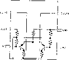
Below, Fig. 1 a and Fig. 1 b represent the circuit diagram of the embodiment of the invention.100 of each figure is the circuit that are applied to the transceiver IC501 of Fig. 5.Specifically, 100 of Fig. 1 a is equivalent to the high frequency band low noise amplifier 502b of Fig. 5, and 100 of Fig. 1 b is equivalent to the low-frequency band low noise amplifier 502a of Fig. 5.
Among Fig. 1 a, the 1st Unit Amplifier 101 is made of transistor 102, bias resistance 103 and load resistance 105.And, have to amplifier 101 biased bias current supply circuits 104.Package pins is high-frequency signal input pin IN1 and 2 grounding leg G1, G2 from emitter.2nd Unit Amplifier 106 paired with amplifier 101 also is same spline structure, is made of transistor 107, bias resistance 108 and load resistance 110.And in the circuit structure identical, also be provided with bias current supply circuit 109 with 104.Pin has input pin IN2, grounding leg G3, G4 too.Power supply and grounding leg are power supply BVcc, and the ground connection BGND of biasing circuit of the power Vcc of amplifier and bias circuit.Even differential amplifier of the grounding leg of Unit Amplifier, except that number of pins reduced, circuit structure was all identical.
Then, the below work of expression amplifier.At first, from the antenna input high-frequency signal.Band pass filter 112 is removed frequency band and is not wanted signal outward, is transformed into differential wave.The match circuit 113,114 of low noise amplifier adopts impedance matching, carries differential wave via pin IN1, IN2 to the differential low noise amplifier of IC inside.104,109 pairs of temperature of bias circuit, current and power supply change generate stable bias current, and the working point of decision transistor 102,107.The bias plasma flow is also identical to 2 circuit.Biasing resistor 103,108 is transformed into voltage to above-mentioned bias current.Therefore, supply with appropriate bias voltage, flow through the direct current collector current and determine transistorized working point to transistor 102,107.Therefore, each transistor carries out the amplification work of differential wave.High-frequency signal after the amplification is converted to voltage by load resistance 105,110, and is sent to the reception blender 115 of back level.
In the differential low noise amplifier that constitutes like this, be shown in the pin configuration of table 1 bottom.Be exactly that the grounding leg of the 1st Unit Amplifier 101 makes the configuration adjacent one to one respectively with the grounding leg of the 2nd Unit Amplifier 106.Therefore, total inductance becomes below half of bonding wire and pin inductance.Its result, shown in 601, the mutual inductance Gm of circuit rises, and gain improves.
Table 3

No.1 in the table 3 and No.2 represent the circuit characteristic analysis result of the configuration of grounding leg shown in the table 1.The No.3 of table 3 is variation of No.2.The No.2 of table 3 and No.3 are the present invention
The pin configuration example of embodiment.
Then, key diagram 1b.Circuit is all identical with Fig. 1 a except that grounding leg becomes a pin, thereby the explanation of the work of omission.To this sort circuit, then carry out the pin configuration shown in table 2 bottom.Be exactly that grounding leg is made the configuration adjacent each other with input pin.Therefore, each emitter impedance of amplifier reduces, and its result has improved the mutual conductance of circuit and improved gain.
Table 4
The No.2 of table 4 is pin configuration of one embodiment of the invention.
High frequency simulation HSPICE has been used in circuit analysis shown in the table 3,4.To the amplifier of analyzing, adopted the bipolar transistor of 0.35 μ m technology.And, under supply voltage 2.8V, flow into the 6ma direct current and carry out work to transistor 102,107.Fig. 2 represents to encapsulate the couple state between a part of pin.The part of 201 expression encapsulation.The pin of 202 expression encapsulation.K is the coupling coefficient of decision mutual conductance amount.The mutual conductance regulation makes coupling coefficient be changed to 0.4,0.27,0.2,0.13 from the effect of pin at first of some pins to three according to its distance.Coupling coefficient supposition is equivalent to QFP (Quadrature Flat Package: square flat packaging) 56 pin.In the table 3, according to present embodiment, the expression gain improves 1.5dB~1.7dB.His-and-hers watches 4 improve gain 1.1dB too.
In order to reduce the inductance composition, it is desirable to the amplifier layout at the circuit that low noise amplifier is set for the shortest position to the distance of pad from the emitter pin top of amplifier transistor.Fig. 3 represents the one example.Fig. 3 is to be example with the double frequency-band transceiver IC that narrated among Fig. 5.The 301st, use transceiver IC chip of the present invention.The 302nd, the QFP56 pin of sealing transceiver IC.The 303rd, the adhesive surface of packaged chip, the 304th, the supporting material of encapsulation.The 305th, the place of using the differential low noise amplifier 502b of high frequency band of the present invention layout.And, the 315th, the differential low noise amplifier 502a of low-frequency band is carried out the place of layout.
306, the 310th, transistor 102 grounding legs of Figure 1A; 307, the 311st, the grounding leg of transistor 107; 308,309 is respectively the input pin of differential low noise amplifier 101 and 106.The 312nd, the supply pin of high frequency band low noise amplifier 502b.
To low-frequency band low noise amplifier 502a too, the 317th, transistor 102 grounding legs of Figure 1B; The 320th, the grounding leg of transistor 107; 318,319 is respectively the input pin of differential low noise amplifier 101 and 106.The 316th, the supply pin of low-frequency band low noise amplifier 502a.The 321st, the supply pin of bias circuit; The 322nd, the grounding leg of bias circuit.The pin of bias circuit is that low frequency low noise amplifier and high frequency low noise amplifier are shared.The 323rd, each pad from the chip is soldered to the bonding wire of the terminal pin shown in above-mentioned.
As shown in Figure 3, amplifier is configured near the central of chip end face and carries out pressure welding.So, the bonding wire between pad and pin will shorten.In the present embodiment, because the supposition double frequency-band distributes from central authorities to the lower end so use the pin of amplifier of the present invention.But grounding leg 306 and 307 is distributed to the pin of middle body.Therefore, the inductance composition comes and will reduce compared with amplifier being configured to chip corner.
So far, narrated LSI, but the present invention also can be applied to the IC that only is made of amplifier with amplifier.At this moment example shown in Fig. 4.The 401st, the differential amplifier IC chip of one embodiment of the invention.The 402nd, the encapsulation TSSOP12 pin of sealing differential amplifier IC.The 403rd, the adhesive surface of packaged chip; The 404th, the encapsulation supporting material.405, the 409th, the grounding leg of transistor 102; 406, the 410th, the grounding leg of transistor 107; 407, the 408th, differential amplifier 101 and 106 input pin.The 411st, the supply pin of bias circuit; The 412nd, the grounding leg of bias circuit; 413, the 414th, the output pin of differential amplifier, the 415th, the supply pin of differential amplifier.The 416th, each pad is soldered to the bonding wire of the above-mentioned terminal pin that illustrates from the chip.
As scheming to the pin of encapsulation central configuration line symmetry, then the distance from the emitter pin top of amplifier transistor to pad just becomes the shortest.And, the low noise differential amplifier is become also comprises the encapsulation electricity influence circuit of symmetry fully.Thereby, can expect that the differential property of IC characteristic is better.
Though Fig. 3,4 according to the pin configuration shown in the No.2 of table 3, also can according to the pin configuration shown in the table 3No.3.
In addition, embodiment describes low noise amplifier as an example, but the present invention is related to the configuration of the grounding leg of amplifier.Therefore, also can be applied to the universal amplifier of difference structure shown in Figure 1A.
According to embodiments of the invention,, in differential amplifier, the grounding leg of the 1st Unit Amplifier is made adjacent one to one with the grounding leg of the 2nd Unit Amplifier respectively configuration with 2 Unit Amplifier for differential amplifier.Therefore, each transistorized emitter inductance is become to below half of single grounding leg.Its result can make each emitter reduce impedance, improves amplifier gain.And, when Unit Amplifier has a grounding leg, can be with grounding leg and input pin configuration adjacent each other.
And, when being applied to resemble the such extensive IC of transceiver IC, becoming the layout of the shortest position and make it combination by the circuit of low noise amplifier being arranged at from the emitter pin top of amplifier transistor the distance of pad, can realize lower inductance.
And, to having only the IC of differential amplifier,, just can make and improve gain by adding the point of two below the present invention, also comprise the symmetrical differential amplifier of encapsulation influence.First point, the distance that the circuit of low noise amplifier is arranged at from the emitter pin top of amplifier transistor to pad becomes the shortest position, and second point makes the pin configuration of symmetry for encapsulation.
Claims (18)
1, a kind of semiconductor device, have semiconductor circuit chip, a plurality of terminal pins that are connected with this semiconductor circuit chip, reach the encapsulation that seals this semiconductor circuit chip, form 2 Unit Amplifier on the above-mentioned semiconductor circuit chip, these 2 Unit Amplifier form 1 differential amplifier
This semiconductor device comprises:
At least 2 earth connections that connect the 1st Unit Amplifier of above-mentioned 2 Unit Amplifier in the above-mentioned a plurality of leads pin; And
At least 2 earth connections that connect the 2nd Unit Amplifier of above-mentioned 2 Unit Amplifier in the above-mentioned a plurality of leads pin,
Wherein, each the terminal pin disposed adjacent of each terminal pin and the earth connection that is connected above-mentioned the 2nd Unit Amplifier that connects the earth connection of above-mentioned the 1st Unit Amplifier.
2, a kind of semiconductor device comprises: have the semiconductor circuit chip of differential amplifier, a plurality of leads pin that is connected with this semiconductor circuit chip, reach the encapsulation that seals described semiconductor circuit chip;
Described differential amplifier has 2 paired together Unit Amplifier, and each Unit Amplifier has signal input part, bias voltage control end, signal output part and power end;
The earth connection of each each Unit Amplifier connects 1 different terminal pin in the described terminal pin respectively; And
Same Unit Amplifier connects the terminal pin and the terminal pin disposed adjacent that is connected incoming line of earth connection.
3, semiconductor device according to claim 1 is characterized in that the terminal pin of the connection earth connection of described 2 Unit Amplifier disposes symmetrically with the Central Line, one side of the terminal pin that is connected incoming line apart from described encapsulation.
4, semiconductor device according to claim 2 is characterized in that the terminal pin of the connection earth connection of described 2 Unit Amplifier disposes symmetrically with the Central Line, one side of the terminal pin that is connected incoming line apart from described encapsulation.
5, semiconductor device according to claim 1 is characterized in that the distance that described 2 Unit Amplifier are configured in from the pad of the earth connection that is connected in these 2 Unit Amplifier to the terminal pin top that protrudes in described package outside is position on the shortest chip.
6, semiconductor device according to claim 2 is characterized in that the distance that described 2 Unit Amplifier are configured in from the pad of the earth connection that is connected in these 2 Unit Amplifier to the terminal pin top that protrudes in described package outside is position on the shortest chip.
7, semiconductor device according to claim 3 is characterized in that the distance that described 2 Unit Amplifier are configured in from the pad of the earth connection that is connected in these 2 Unit Amplifier to the terminal pin top that protrudes in described package outside is position on the shortest chip.
8, semiconductor device according to claim 4 is characterized in that the distance that described 2 Unit Amplifier are configured in from the pad of the earth connection that is connected in these 2 Unit Amplifier to the terminal pin top that protrudes in described package outside is position on the shortest chip.
9, semiconductor device according to claim 1, each comprises to it is characterized in that described 2 Unit Amplifier: the transistor that is connected with described earth connection, power line, and load; And
Described load is connected between the described power line of described transistor AND gate.
10, semiconductor device according to claim 2, each comprises to it is characterized in that described 2 Unit Amplifier: the transistor that is connected with described earth connection, power line, and load; And
Described load is connected between the described power line of described transistor AND gate.
11, semiconductor device according to claim 3, each comprises to it is characterized in that described 2 Unit Amplifier: the transistor that is connected with described earth connection, power line, and load; And
Described load is connected between the described power line of described transistor AND gate.
12, semiconductor device according to claim 4, each comprises to it is characterized in that described 2 Unit Amplifier: the transistor that is connected with described earth connection, power line, and load; And
Described load is connected between the described power line of described transistor AND gate.
13, semiconductor device according to claim 5, each comprises to it is characterized in that described 2 Unit Amplifier: the transistor that is connected with described earth connection, power line, and load; And
Described load is connected between the described power line of described transistor AND gate.
14, semiconductor device according to claim 6, each comprises to it is characterized in that described 2 Unit Amplifier: the transistor that is connected with described earth connection, power line, and load; And
Described load is connected between the described power line of described transistor AND gate.
15, semiconductor device according to claim 7, each comprises to it is characterized in that described 2 Unit Amplifier: the transistor that is connected with described earth connection, power line, and load; And
Described load is connected between the described power line of described transistor AND gate.
16, a kind of semiconductor device that is used for the radio communication transmitting-receiving comprises:
Be arranged on received signal and the signal from local oscillator from antenna are carried out the receiving mixer of mixing and the differential low noise amplifier between the described antenna, with a plurality of leads pin that is connected with this differential low noise amplifier;
This differential low noise amplifier has 2 Unit Amplifier that input phase is anti-phase mutually and signal band is identical, and each Unit Amplifier has signal input part, bias voltage control end, signal output part and power end; And
The earth connection of described 2 Unit Amplifier connects mutually different terminal pin respectively;
The described terminal pin disposed adjacent that connects earth connection, perhaps
One of terminal pin of the described earth connection of connection of same Unit Amplifier and the terminal pin disposed adjacent that is connected incoming line.
17, according to the described semiconductor device that is used for the radio communication transmitting-receiving of claim 16, it is characterized in that the earth connection of described 2 Unit Amplifier connects a plurality of leads pin respectively.
18,, it is characterized in that each each disposed adjacent of a plurality of leads pin that is connected with the earth connection of another Unit Amplifier of a plurality of leads pin of the earth connection connection of a Unit Amplifier in described 2 Unit Amplifier according to the described semiconductor device that is used for the radio communication transmitting-receiving of claim 17.
Applications Claiming Priority (2)
| Application Number | Priority Date | Filing Date | Title |
|---|---|---|---|
| JP265982/2000 | 2000-08-30 | ||
| JP2000265982A JP4319339B2 (en) | 2000-08-30 | 2000-08-30 | Semiconductor device |
Publications (2)
| Publication Number | Publication Date |
|---|---|
| CN1340858A CN1340858A (en) | 2002-03-20 |
| CN1227733C true CN1227733C (en) | 2005-11-16 |
Family
ID=18753157
Family Applications (1)
| Application Number | Title | Priority Date | Filing Date |
|---|---|---|---|
| CNB011258381A Expired - Fee Related CN1227733C (en) | 2000-08-30 | 2001-08-29 | Semiconductor device |
Country Status (6)
| Country | Link |
|---|---|
| US (1) | US6624509B2 (en) |
| EP (1) | EP1187208A3 (en) |
| JP (1) | JP4319339B2 (en) |
| KR (1) | KR100750449B1 (en) |
| CN (1) | CN1227733C (en) |
| TW (1) | TW516268B (en) |
Families Citing this family (22)
| Publication number | Priority date | Publication date | Assignee | Title |
|---|---|---|---|---|
| JP2002076267A (en) * | 2000-08-22 | 2002-03-15 | Hitachi Ltd | Radio transmitter |
| US20020127992A1 (en) * | 2001-03-08 | 2002-09-12 | Fransis Bert L. | Wideband local oscillator architecture |
| US20020127985A1 (en) * | 2001-03-08 | 2002-09-12 | Fransis Bert L. | Wideband local oscillator architecture |
| US6751470B1 (en) * | 2002-04-08 | 2004-06-15 | Nokia Corporation | Versatile RF front-end multiband mobile terminals |
| KR100993277B1 (en) | 2002-04-30 | 2010-11-10 | 르네사스 일렉트로닉스 가부시키가이샤 | Semiconductor device and electronic device |
| WO2003094236A1 (en) * | 2002-04-30 | 2003-11-13 | Renesas Technology Corp. | Semiconductor device and radio communication apparatus |
| KR100993579B1 (en) | 2002-04-30 | 2010-11-10 | 르네사스 일렉트로닉스 가부시키가이샤 | Semiconductor device and electronic device |
| JP4149438B2 (en) * | 2002-06-05 | 2008-09-10 | 株式会社ルネサステクノロジ | Semiconductor device |
| KR100499788B1 (en) * | 2002-11-27 | 2005-07-07 | 인티그런트 테크놀로지즈(주) | Integrated Circuit Chip |
| JP4137059B2 (en) * | 2003-02-14 | 2008-08-20 | 株式会社ルネサステクノロジ | Electronic device and semiconductor device |
| TWI225332B (en) * | 2003-05-20 | 2004-12-11 | Mediatek Inc | Multi-band low noise amplifier |
| JP2005006031A (en) * | 2003-06-11 | 2005-01-06 | Sony Corp | Amplifier and receiving circuit |
| KR101014708B1 (en) * | 2003-08-27 | 2011-02-16 | 엘지전자 주식회사 | structure of rotary knob assembly in Washing machine |
| JP4418250B2 (en) * | 2004-02-05 | 2010-02-17 | 株式会社ルネサステクノロジ | High frequency circuit module |
| JP2006073821A (en) * | 2004-09-02 | 2006-03-16 | Sharp Corp | Semiconductor integrated circuit device |
| JP2008218776A (en) * | 2007-03-06 | 2008-09-18 | Renesas Technology Corp | Semiconductor device |
| US8085596B2 (en) * | 2007-09-11 | 2011-12-27 | Micron Technology, Inc. | Reducing noise in semiconductor devices |
| JP5588147B2 (en) * | 2009-10-26 | 2014-09-10 | キヤノン株式会社 | Semiconductor device and printed circuit board mounted with semiconductor device |
| JP5499696B2 (en) * | 2009-12-25 | 2014-05-21 | 富士通セミコンダクター株式会社 | Semiconductor device and mounting structure |
| WO2016185426A1 (en) * | 2015-05-20 | 2016-11-24 | Wizedsp Ltd. | An ultra-low-power and low-noise amplifier |
| CN106936431B (en) * | 2015-12-30 | 2021-07-20 | 上海贝岭股份有限公司 | High-performance low-noise chip and manufacturing method thereof |
| IT201600086488A1 (en) * | 2016-08-22 | 2018-02-22 | St Microelectronics Srl | SEMICONDUCTOR DEVICE AND CORRESPONDENT PROCEDURE |
Family Cites Families (10)
| Publication number | Priority date | Publication date | Assignee | Title |
|---|---|---|---|---|
| JP2716005B2 (en) * | 1995-07-04 | 1998-02-18 | 日本電気株式会社 | Wire bond type semiconductor device |
| KR0156334B1 (en) * | 1995-10-14 | 1998-10-15 | 김광호 | Semiconductor chip package having shield bonding wire for high frequency and high density |
| JPH1075132A (en) * | 1996-08-29 | 1998-03-17 | Mitsumi Electric Co Ltd | Differential amplifier |
| US5789799A (en) * | 1996-09-27 | 1998-08-04 | Northern Telecom Limited | High frequency noise and impedance matched integrated circuits |
| JP3920427B2 (en) * | 1997-11-19 | 2007-05-30 | 富士通株式会社 | Differential amplifier circuit and operational amplifier circuit |
| WO1999027646A1 (en) * | 1997-11-21 | 1999-06-03 | Hitachi, Ltd. | High-frequency amplifier circuit device and high-frequency transmission system using the same |
| JPH11163644A (en) * | 1997-11-26 | 1999-06-18 | Fujitsu Ltd | Output circuit using differential amplifier circuit |
| US6094084A (en) * | 1998-09-04 | 2000-07-25 | Nortel Networks Corporation | Narrowband LC folded cascode structure |
| JP2000299438A (en) * | 1999-04-15 | 2000-10-24 | Hitachi Ltd | Semiconductor integrated circuit |
| JP4018312B2 (en) * | 2000-02-21 | 2007-12-05 | 株式会社ルネサステクノロジ | Wireless communication device |
-
2000
- 2000-08-30 JP JP2000265982A patent/JP4319339B2/en not_active Expired - Fee Related
-
2001
- 2001-05-04 TW TW090110764A patent/TW516268B/en not_active IP Right Cessation
- 2001-07-25 US US09/911,796 patent/US6624509B2/en not_active Expired - Lifetime
- 2001-08-03 EP EP01118714A patent/EP1187208A3/en not_active Withdrawn
- 2001-08-29 CN CNB011258381A patent/CN1227733C/en not_active Expired - Fee Related
- 2001-08-30 KR KR1020010052874A patent/KR100750449B1/en not_active IP Right Cessation
Also Published As
| Publication number | Publication date |
|---|---|
| JP4319339B2 (en) | 2009-08-26 |
| US6624509B2 (en) | 2003-09-23 |
| EP1187208A3 (en) | 2011-09-07 |
| KR20020018146A (en) | 2002-03-07 |
| TW516268B (en) | 2003-01-01 |
| KR100750449B1 (en) | 2007-08-22 |
| CN1340858A (en) | 2002-03-20 |
| US20020053729A1 (en) | 2002-05-09 |
| JP2002076235A (en) | 2002-03-15 |
| EP1187208A2 (en) | 2002-03-13 |
Similar Documents
| Publication | Publication Date | Title |
|---|---|---|
| CN1227733C (en) | Semiconductor device | |
| Reynolds et al. | 60GHz transceiver circuits in SiGe bipolar technology | |
| US6847108B2 (en) | Semiconductor integrated circuit | |
| EP3051587B1 (en) | Cmos transceiver having an integrated power amplifier | |
| US5698469A (en) | Method of making a hybrid circuit with a chip having active devices with extra-chip interconnections | |
| CN109818581B (en) | Multi-path amplifier with series components of inverters along output terminals of the amplifier | |
| CA2236993C (en) | Hybrid circuit construction of push-pull power amplifier | |
| US5610563A (en) | Slot line to CPW circuit structure | |
| US7106093B2 (en) | Semiconductor device | |
| CN1476650A (en) | Radio frequency amplifying circuit | |
| CN117546407A (en) | Output integrated transistor amplifier device package incorporating internal connections | |
| CN102299686B (en) | Inductive circuit arrangement | |
| US11190146B2 (en) | Doherty power amplifier devices having intergrated output combining networks | |
| EP1058380A2 (en) | Push-pull amplifier with dual coplanar transmission line | |
| WO2005034240A1 (en) | Module integration integrated circuits | |
| Sevenhans | Silicon radio integration: architectures and technology: from cartesian zero IF receive & transmit to polar zero I and Q, from silicon bipolar to bulk and SOI CMOS | |
| Boers | 60 GHz silicon transmitters | |
| AU694066C (en) | Method for making a circuit structure having a flip-mounted matrix of devices | |
| CA2236983C (en) | Slotline-to-coplanar waveguide transition |
Legal Events
| Date | Code | Title | Description |
|---|---|---|---|
| C06 | Publication | ||
| PB01 | Publication | ||
| C10 | Entry into substantive examination | ||
| SE01 | Entry into force of request for substantive examination | ||
| C14 | Grant of patent or utility model | ||
| GR01 | Patent grant | ||
| CF01 | Termination of patent right due to non-payment of annual fee |
Granted publication date: 20051116 Termination date: 20140829 |
|
| EXPY | Termination of patent right or utility model |