CN1225085C - Formation of pulse signal from clock signal - Google Patents
Formation of pulse signal from clock signal Download PDFInfo
- Publication number
- CN1225085C CN1225085C CNB011436093A CN01143609A CN1225085C CN 1225085 C CN1225085 C CN 1225085C CN B011436093 A CNB011436093 A CN B011436093A CN 01143609 A CN01143609 A CN 01143609A CN 1225085 C CN1225085 C CN 1225085C
- Authority
- CN
- China
- Prior art keywords
- mentioned
- delay
- pulse signal
- signal
- clock signal
- Prior art date
- Legal status (The legal status is an assumption and is not a legal conclusion. Google has not performed a legal analysis and makes no representation as to the accuracy of the status listed.)
- Expired - Fee Related
Links
Images


Classifications
-
- H—ELECTRICITY
- H03—ELECTRONIC CIRCUITRY
- H03K—PULSE TECHNIQUE
- H03K5/00—Manipulating of pulses not covered by one of the other main groups of this subclass
- H03K5/13—Arrangements having a single output and transforming input signals into pulses delivered at desired time intervals
- H03K5/131—Digitally controlled
-
- H—ELECTRICITY
- H03—ELECTRONIC CIRCUITRY
- H03K—PULSE TECHNIQUE
- H03K5/00—Manipulating of pulses not covered by one of the other main groups of this subclass
- H03K5/13—Arrangements having a single output and transforming input signals into pulses delivered at desired time intervals
- H03K5/135—Arrangements having a single output and transforming input signals into pulses delivered at desired time intervals by the use of time reference signals, e.g. clock signals
Landscapes
- Physics & Mathematics (AREA)
- Nonlinear Science (AREA)
- Pulse Circuits (AREA)
- Synchronisation In Digital Transmission Systems (AREA)
- Manipulation Of Pulses (AREA)
Abstract
Providing technology capable of satisfying a request value concerning the specified period of a pulse signal, without excessively lowering the cycle of a clock signal, even if considering fluctuation in delay time is taken into consideration, in a delay element. Two first delay signals Q30 and Q34 are generated such that edges thereof are delayed by a first delay time Td1 in relation to the rising edge of a clock signal CLK. Two second delay signals Q32 and Q36 are also generated such that edges thereof are delayed by a second delay time Td2 in relation to the trailing edge of the clock signal CLK. A pulse signal Sout is generated as a result of logic operations performed on the first delay signals Q30 and Q34 and the second delayed signals Q32 and Q36.
Description
Technical field
The present invention relates to generate the technology of specific pulse signal from the clock signal of some cycles.
Background technology
Figure 13 illustrates the block diagram that is used for generating from clock signal clk traditional pulse signal generative circuit 200 1 examples of specific pulse signal Q230.This circuit 200 possesses d type flip flop 210 (hereinafter referred to as " DFF210 "), and a side of 220,222,2 input terminals of 2 delay elements that are connected in series becomes the NAND door 230 of reversed input terminal.Clock signal clk is provided to the clock input terminal of DFF210.The output Q210 of DFF210 is input to the 1st and prolongs element spare 220, and anti-phase output #Q210 feeds back to the D input terminal.The inhibit signal Q220 that has postponed in the 1st delay element 220 is input to the in-phase input terminal of NAND door 230.In addition, this inhibit signal Q220 is input to the reversed input terminal of NAND door 230 after further having been postponed by the 2nd delay element 222.
Figure 14 (a) is the flow chart that the action of this pulse signal generative circuit 220 is shown to (e).From the 1st inhibit signal Q220 (Figure 14 (c)) of the 1st delay element 220 output had from the rise edge delay of clock signal clk the 1st time of delay Td1 the edge.In addition, from the 2nd inhibit signal Q222 (Figure 14 (d)) of the 2nd delay element 222 output have from the rising edge of the 1st inhibit signal Q220 further postponed the 2nd time of delay Td2 the edge.Thereby, the edge of the 2nd inhibit signal Q222 from the rise edge delay of clock signal clk time of delay (Td1+Td2).NAND door 230 generates the pulse signal Q230 (Figure 14 (e)) shown in Figure 14 (e) from these 2 inhibit signal Q220, Q222.
This pulse signal 230 for example uses as the write control signal of RAM.That is, pulse signal 230 is designed in 1 period T c of clock signal clk, and only Tw becomes the signal of L level during specific.Before being about to begin this period T w, set Ts settling time, in addition, during being right after, set retention time Th after the Tw.These time T s, Tw, Th set the required value in the design respectively for.Td1, Td2 were set at and made Ts, Tw during these, Th satisfy required value separately 2 time of delay.
But, in the design of this circuit, generally consider delay time dispersion such as the foozle of delay element 220,222 or temperature dependency, think to exist sizable error among Td1, the Td2 in time of delay.Therefore, in circuit design in the past shown in Figure 13, be difficult to set Td1 time of delay, Td2, make Ts, Tw during these, Th satisfy required value separately.Here, suppose during 3, to set among Ts, Tw, the Th situation of following required value:
Condition C 1:Ts 〉=1ns;
Condition C 2:Tw 〉=10ns;
Condition C 3:Th 〉=3ns.
And because the value from standard value (representative value) about 0.6 times to about 1.6 times is got in the change of Td1 time of delay, Td2 that temperature characterisitic etc. causes usually.Thereby, time of delay Td1, Td2 maximum can become about 2.7 times of minimum value (=1.6/0.6) about.If consider such error, then above-mentioned condition C 1, C3 can rewrite as follows:
Condition C 1a:Ts=Td1=1ns (min)~2.7ns (max);
Condition C 2a:Tw=Td2=10ns (min)~27ns (max);
Condition C 3a:Th 〉=3ns.
Here, (min) mean that Td1 time of delay, Td2 become the condition of minimum value, mean that (max) Td1 time of delay, Td2 become peaked condition.Thereby, time of delay Td1, Td2 each all become in the peaked condition, clock cycle Tc become about 33ns (=2.7+27+3), this is equivalent to about 30MHz.On the other hand, (=1+10+3) ns, this is about as much as 71MHz to be 14 from the minimum value (cycle period of RAM) of the clock cycle Tc that above-mentioned condition C 1a~C3a determined.That is,, when in the circuit of Figure 13, generating write control signal, this RAM is moved with about 30MHz (about 42% speed) even use the RAM that can move with about 71MHz.
Like this, in pulse signal generative circuit in the past,, consider the change of the time of delay in the delay element, exist and to reduce the problem in the cycle of clock signal greatly for the required value between the given period that satisfies relevant pulse signal.
Summary of the invention
The present invention produces for solving above-mentioned problem in the past, even purpose is to provide the change of considering the time of delay in the delay element, also can reduce the cycle of clock signal within bounds, satisfy the technology of the required value between the given period of relevant pulse signal.
To achieve the above object, the invention provides the circuit that is used for generating specific pulse signal, it is characterized in that possessing: the edge detection unit that is used to detect above-mentioned rising edge of clock signal and trailing edge from clock signal with some cycles; The 1st inhibit signal generation unit has at least 1 the 1st delay element that includes the 1st retardation, is used to generate at least 1 and includes from above-mentioned rising edge of clock signal and the 1st postpone the 1st inhibit signal at edge with what the 1st above-mentioned retardation had postponed; The 2nd inhibit signal generation unit has at least 1 the 2nd delay element that includes the 2nd retardation, is used to generate at least 1 and includes from the trailing edge of above-mentioned clock signal and the 2nd postpone the 2nd inhibit signal at edge with what the 2nd above-mentioned retardation had postponed; Can generate the arithmetic logic unit of above-mentioned pulse signal by the logical operation of carrying out above-mentioned at least 1 the 1st inhibit signal and above-mentioned at least 1 the 2nd inhibit signal.
In this pulse signal generative circuit, generate the 1st inhibit signal from rising edge of clock signal, generate the 2nd inhibit signal from the trailing edge of clock signal, by carrying out the logical operation production burst signal of these inhibit signals, therefore with only compared like that from the situation of rising edge of clock signal production burst signal in the past, can reduce the influence of the change of retardation.Its result even consider the change of the retardation in the delay element, also can reduce the cycle of clock signal within bounds with the required value between the given period that satisfies relevant pulse signal.
In addition, 1 of above-mentioned pulse signal cycle preferably is set at identical with 1 cycle of above-mentioned clock signal.In this structure, can since the influence of the change pulse signals of retardation suppress for very little.
In addition, the above-mentioned the 1st and the 2nd retardation preferably is set at 1/2 value less than 1 cycle of above-mentioned clock signal respectively.In this structure,, therefore can also suppress the change of the retardation that causes owing to temperature characterisitic etc. very for a short time because retardation itself is little.
And then the above-mentioned the 1st and the 2nd retardation preferably equates mutually.In this structure, even retardation change can remain almost certain during between the edge of the edge of the pulse signal that is determined by the 1st retardation and the pulse signal that determined by the 2nd retardation.
In addition, above-mentioned edge detection unit can also comprise: the 1D trigger, it has the 1st clock input terminal, 1D input terminal, the 1st lead-out terminal and the 1st reversed-phase output, when above-mentioned clock signal is input to the 1st clock input terminal, feed back to above-mentioned 1D input terminal from the anti-phase output of above-mentioned the 1st reversed-phase output; The 2nd trigger, it has the 2nd clock input terminal, 2D input terminal, the 2nd lead-out terminal and the 2nd reversed-phase output, inversion clock signal after above-mentioned clock signal is anti-phase is input in above-mentioned the 2nd clock input terminal, is imported into above-mentioned 2D input terminal from the output of above-mentioned the 1st lead-out terminal of above-mentioned 1D trigger.At this moment, when the output from above-mentioned the 1st lead-out terminal of above-mentioned 1D trigger is imported into above-mentioned the 1st delay element, be imported into above-mentioned the 2nd delay element from the output of above-mentioned the 2nd lead-out terminal of above-mentioned 2D trigger.
In this structure, can detect rising edge of clock signal and trailing edge well.
In addition, the present invention can also realize with all forms, for example, realize with forms such as pulse signal generative circuit or pulse signal generation methods.
Description of drawings
Fig. 1 is the block diagram that pulse signal generative circuit 100 structures of the 1st embodiment are shown.
Fig. 2 is the flow chart of action that the pulse signal generative circuit 100 of the 1st embodiment is shown.
Fig. 3 be illustrated in with comparing the 1st time of delay Td1 than Td2 hour the 2nd time of delay, get minimum value time of delay and get the key diagram of peaked situation.
Fig. 4 be illustrated in with comparing the 1st with the 2nd time of delay Td1, when Td2 equates, get minimum value time of delay and get the key diagram of peaked situation.
Fig. 5 be illustrated in with comparing the 1st time of delay Td1 when the 2nd time of delay, Td2 was big, get minimum value time of delay and get the key diagram of peaked situation.
Fig. 6 illustrates the key diagram that transmits the example that uses pulse signal Q40 for the data of carrying out external bus.
Fig. 7 is the structured flowchart that the pulse signal generative circuit 110 of the 2nd embodiment is shown.
Fig. 8 is the flow chart of action that the pulse signal generative circuit 110 of the 2nd embodiment is shown.
Fig. 9 is the block diagram of structure that the pulse signal generative circuit 120 of the 3rd embodiment is shown.
Figure 10 is the block diagram of structure that the pulse signal generative circuit 130 of the 4th embodiment is shown.
Figure 11 is the block diagram of structure that the pulse signal generative circuit 140 of the 5th embodiment is shown.
Figure 12 is the block diagram of structure that the pulse signal generative circuit 150 of the 6th embodiment is shown.
Figure 13 is the block diagram that pulse signal generative circuit 200 1 examples in the past are shown.
Figure 14 is the flow chart that the action of pulse signal generative circuit 200 in the past is shown.
Embodiment
Below, according to embodiment embodiments of the present invention are described according to following order:
A. the 1st embodiment;
B. the 2nd embodiment;
C. the 3rd embodiment;
D. the 4th embodiment;
E. the 5th embodiment;
F. the 6th embodiment;
G. variation
A. the 1st embodiment:
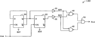
Fig. 1 is the block diagram that illustrates as the structure of the pulse signal generative circuit 100 of the present invention the 1st embodiment.The side that this pulse signal generative circuit 100 possesses 30,32,2 input terminals of 20,22,2 delay elements of 2 d type flip flops becomes the NAND door 40 of in-phase input terminal.In addition, below, " d type flip flop " called " DFF ".
When clock signal clk is input to the clock input terminal of 1DFF20, be input to the clock terminal of 2DFF22 after anti-phase.The anti-phase output #Q20 of 1DFF20 feeds back to the D input terminal of 1DFF20.When the output Q20 of 1DFF20 is input to the D input terminal of 2DFF22, also be input to the 1st delay element 30.The output Q22 of 2DFF20 is input to the 2nd delay element 32.The 1st inhibit signal Q30 that has been postponed by the 1st delay element 30 is input to the in-phase input terminal of NAND door 40.In addition, the 2nd inhibit signal Q32 that has been postponed by the 2nd delay element 32 is input to the reversed input terminal of NAND door 40.In addition, therefore 2 DFF20,22 are taken as the L level at initial condition their output Q20, Q22 owing to be reset in initial condition.
Fig. 2 is the flow chart of action that the pulse signal generative circuit 100 of the 1st embodiment is shown.The output Q20 of 1DFF20 (Fig. 2 (b)) is that rising edge at each clock signal clk is the signal of level inversion.On the other hand, the output Q22 of 2DFF22 (Fig. 2 (c)) is that trailing edge at each clock signal clk is the signal of level inversion.
The output Q20 of 1DFF20 becomes the 1st inhibit signal Q30 (Fig. 2 (d)) by the 1st delay element 30 delay controls Td1 1 time of delay.On the other hand, the output Q22 of 2DFF22 becomes the 2nd inhibit signal Q32 (Fig. 2 (e)) by the 2nd delay element 32 delay controls Td2 2 time of delay.That is, the 1st inhibit signal Q30 be have begun to postpone from the above-mentioned edge of clock signal clk the 1st time of delay Td1 the signal at edge.In addition, the 2nd inhibit signal Q32 be have from the trailing edge of clock signal clk begun to postpone the 2nd time of delay Td2 the signal at edge.NAND door 40 is by carrying out logical operation to these inhibit signals Q30, Q32, production burst signal Q40 (Fig. 2 (f)).
The trailing edge of pulse signal Q40 is from the rise edge delay Td1 the 1st time of delay of clock signal clk.In addition, the rising edge of pulse signal Q40 is from the trailing edge delay control Td2 2 time of delay of clock signal clk.Like this, in the pulse signal generative circuit 100 of the 1st embodiment, delay by different types of edge of identical clock signal clk generates respectively the trailing edge of pulse signal Q40 with rising edge, therefore has can reduce because the advantage of the influence of the pulse signals that the error of time of delay causes.Its result, as following illustrated, compared with the pastly the period T c of clock signal clk can be designed shortly.
Here, identical with the above-mentioned example that illustrated in the prior art, in from Ts, Tw, Th during 3 of the output signal Q40 (Fig. 2 (f)) of NAND door 40, suppose to set respectively following such condition C 1~C3:
Condition C 1:Ts 〉=1ns;
Condition C 2:Tw 〉=10ns;
Condition C 3:Th 〉=3ns.
As can understanding from Fig. 2 (f), during these period T c of Ts, Tw, Th and clock signal clk and time of delay Td1, Td2 have the relation of following (1)~(3) formula:
Ts=Td1…(1)
Tw=Td2+Tc/2-Td1…(2)
Th=Tc/2-Td2…(3)。
At this moment, above-mentioned condition C 1~C3 can be rewritten as following condition C 4~C6:
Condition C 4:Ts=Td1 〉=1ns;
Condition C 5:Tw=Td2+Tc/2-Td1 〉=10ns;
Condition C 6:Th=Tc/2-Td2 〉=3ns.
Here, the 1st time of delay Td1 maximum of T d1max supposition be 2.7 times of its minimum value Td1min, the 2nd time of delay Td2 maximum of T d2max also suppose it is 2.7 times of its minimum value Td2min.In addition, suppose that the opposing party also got minimum value when a side among 2 time of delays Td1, the Td2 got minimum value, the opposing party also got maximum when a side got maximum.The latter's supposition is to consider in the maximum or minimum value of time of delay, is comprising the relation of delay element 30,32 temperature dependent influences.Promptly, if when not considering that a side delay element is got maximum under temperature dependent influence, the opposing party's delay element is got the such situation of minimum value under temperature dependent influence, then both sides to get minimum value simultaneously or get peaked consideration simultaneously be appropriate.
But above-mentioned condition C 4 is the strictest when Td1 gets its minimum value Td1min in the 1st time of delay.In addition, above-mentioned condition C 6 the 2nd time of delay Td2 to get its maximum of T d2max (the strictest=2.7 * Td2min) time.Thereby condition C 4~C6 can be rewritten as following condition C 4a~C6a:
Condition C 4a:Ts=Td1min 〉=1ns;
Condition C 5a:Tw=Td2+Tc/2-Td1 〉=10ns;
Condition C 6a:Th=Tc/2-2.7 * Td2min 〉=3ns.
Here, suppose time of delay Td1, when Td2 gets its minimum value Td1min, Td2min respectively, during Tw become 10ns.At this moment, following (4)~(6) formula is set up:
Td1min≥1ns…(4)
Td2min+Tc/2-Td1min=10ns…(5)
Tc/2-2.7×Td2min≥3ns…(6)。
If (5) formula is updated in (4) formula, then can obtain following (7) formula:
Td2min+Tc/2≥11ns…(7)。
If (6) formula and (7) formula are found the solution for Tc, then can be obtained following (8) formula:
Tc≥17.7ns…(8)。
Here, if consider Td1=1ns, Tc=17.7ns, then from (5) formula, Td2min becomes 2.15ns.At Tc=17.7ns, Td1=Td1min=1ns during Td2=Td2min=2.15ns, can confirm easily that above-mentioned condition C 4~C6 sets up.
On the other hand and since time of delay Td1, Td2 maximum of T d1max, Td2max be respectively its minimum value Td1min, Td2min 2.7 times, therefore become 2.7ns and 5.8ns respectively.When this maximum condition, that is, Tc=17.7ns, Td1=Td1max=2.7ns during Td2=Td2max=5.8ns, can confirm that also above-mentioned condition C 4~C6 sets up.Thereby, even clock cycle Tc is set at 17.7ns (56.5MHz) if consider the change of Td1 time of delay, Td2, then can satisfy pulse signal Q40 respectively during the required value of Ts, Tw, Th.
(=1+10+3) ns, this is equivalent to about 71MHz and the minimum value of the clock cycle Tc that is determined from above-mentioned condition C 1~C3 is 14.Different therewith, in the present embodiment,, also can be set at 17.7ns (56.5MHz) to the clock cycle even consider the change of time of delay.For example, when the write control signal that this pulse signal Q40 is used as RAM, can carry out work with about 80% frequency of the maximum possible operating frequency (71MHz) of RAM.On the other hand, as illustrated mistake in the prior art, in circuit in the past shown in Figure 13, only can carry out work with about 42% frequency (30MHz) of the maximum possible operating frequency of RAM.That is, in the circuit of the 1st embodiment, compare, can generate the pulse signal of about 1.9 overtones bands with circuit in the past shown in Figure 13.
As can understanding from above explanation, in the circuit of the 1st embodiment, even consider Td1 time of delay of delay element 30,32, the change of Td2, also can reduce clock cycle Tc within bounds, satisfy the required value during each of relevant pulse signal Q40.
Wherein, time of delay, Td1, Td preferably were set at 1/2 value less than clock cycle Tc.It is the reasons are as follows: for example, Td1 is 1/2 when above of clock cycle Tc in time of delay, and the trailing edge of pulse signal Q40 takes place later at the trailing edge of clock signal clk.Thereby, at this moment, can be from the trailing edge of the trailing edge production burst signal Q40 of clock signal clk.In other words, Td1 is 1/2 when above of clock cycle Tc in time of delay, calculate from time of delay Td1 deduct time (Td1-Tc/2) of the half period Tc/2 of clock signal clk, can postpone at trailing edge from clock signal clk should the time (Td1-Tc/2) the moment, the trailing edge of pulsing signal Q40.And in the method, Td1 is that the situation more than 1/2 of clock cycle Tc is compared to have and reduced because the advantage of the influence that the change of time of delay produces with time of delay.Thereby in the circuit of Fig. 1, time of delay, Td1, Td2 preferably were set at 1/2 value less than clock cycle Tc.
Yet, during the L level of pulse signal Q40 Tw according to time of delay Td1, Td2 change change, the mode of its variation because of 2 time of delay Td1, Td2 magnitude relationship different.Fig. 3 be comparatively illustrate the 1st time of delay Td1 than Td2 hour the 2nd time of delay, time of delay Td1, (Fig. 3 (b)) and the key diagram of (Fig. 3 (c)) when getting maximum when Td2 gets minimum value respectively.Can understand the 1st time of delay Td1 than Td2 hour the 2nd time of delay, the situation when getting minimum value with time of delay is compared and is got, during maximum during Tw long.
Fig. 4 be comparatively illustrate the 1st with the 2nd time of delay Td1, when Td2 equates, time of delay Td1, the key diagram when Td2 gets minimum value respectively when getting maximum respectively.When 2 time of delays, Td1, Td2 equated, though change time of delay, during the length of Tw also roughly keep certain.
Fig. 5 be comparatively illustrate the 1st time of delay Td1 when the 2nd time of delay, Td2 was big, time of delay Td1, the key diagram when Td2 gets minimum value respectively when getting maximum respectively.The 1st time of delay Td1 when the 2nd time of delay, Td2 was big, compare with the situation of getting minimum value time of delay, when getting maximum during Tw short.
Like this, time of delay Td1, Td2 change for during Tw (that is, by the rise edge delay that makes clock signal clk delay edge that obtains and the delay edge that makes trailing edge postpone to obtain fold during) the influence of length depend on the magnitude relationship of Td1 time of delay, Td2.Thereby, preferably according to during the condition of required value of Tw, suitably set the magnitude relationship of Td1 time of delay, Td2.For example, for the length of guaranty period Tw all the time is roughly certain, preferably time of delay Td1, Td2 be set at equal.
Pulse signal Q40 not only can be utilized as the control that writes of RAM, and can also utilize in other purposes.Fig. 6 illustrates the key diagram as an example of the strobe pulse use that is used for the data transmission on the data/address bus pulse signal Q40.Fig. 6 (b) illustrates Td1 time of delay, Td2 and gets pulse signal Q40 under the minimum conditions, and Fig. 6 (d) is illustrated in the sequential of the data-signal on the data/address bus under this condition.In addition, Fig. 6 (c) illustrates Td1 time of delay, Td2 and gets pulse signal Q40 under the maximum condition, and Fig. 6 (e) is illustrated in the sequential of the data-signal on the data/address bus under this condition.
As can understanding from this example, when time of delay Td1, Td2 because former thereby changes such as temperature dependencies, and during the timing variations of corresponding pulse signal Q40, the sequential of the data-signal on the data/address bus also changes with identical therewith tendency.That is, though the trailing edge from the change point of data-signal to pulse signal Q40 during Tp or change point from the rising edge of pulse signal Q40 to data-signal during Tq be subjected to because the influence that temperature produces also keeps the length more than certain.Thereby,,, also can carry out data reliably and transmit if pulse signal Q40 is used as strobe pulse even the sequential of data-signal changes under the influence of temperature dependency etc.In addition, as described above, if the circuit 100 of foundation the 1st embodiment then owing to can be the frequency setting of pulse signal Q40 than big in the past value, therefore can carry out data at high speed and transmit.
B: the 2nd embodiment:
Fig. 7 is the block diagram of structure that the pulse signal generative circuit 110 of the present invention the 2nd embodiment is shown.This pulse signal generative circuit 110 has front stage circuits 112 and late-class circuit 114 and AND door 50.Front stage circuits 112 has the structure identical with the pulse signal generative circuit 100 of the 1st embodiment shown in Figure 1.The side that late-class circuit 114 has 2 DFF24,34,36,2 input terminals of 26,2 delay elements becomes the NAND door 42 of reversed input terminal.Connection status between each element in the late-class circuit 114 basically with front stage circuits 112 in each element between connection status identical.In addition, the delay elements 34,36 in the late-class circuit 114 have respectively and identical Td1 time of delay, the Td2 of delay element 30,32 in the front stage circuits 112.But input is from the output Q22 of the 2DFF22 in the front stage circuits 112 on the D input terminal of the 1DFF24 in late-class circuit 114.In addition, different with the 1DFF20 of front stage circuits 112, the anti-phase output of the 1DFF24 of late-class circuit 114 does not feed back to the D input terminal of DFF24.In addition, because 2 DFF24,26 in the late-class circuit 114 are set in initial condition, therefore get the H level at initial condition their output Q24, Q26.AND door 50 generates final pulse signal Sout by getting the logic product of front stage circuits 112 and output Q40, the Q42 (i.e. the output of 2 NAND doors 40,42) of late-class circuit 114.
Fig. 8 is the action flow chart that the pulse signal generative circuit 110 of the 2nd embodiment is shown.Signal CLK, Q30, Q32, Q40 shown in Fig. 8 (a) and (b), (c), (d) are the signals of front stage circuits 112, be respectively with the identical signal of respective signal shown in Fig. 2 (a), (d), (e), (f) in the 1st embodiment.In addition, signal Q34, Q36, Q42 shown in Fig. 8 (e), (f), (g) are the signals of late-class circuit 114, become signal Q30, the Q32 from front stage circuits 112, the signal that Q40 has moved clock cycle Tc respectively backward.For example, be equivalent to pulse signal among the odd number period T c, be equivalent to pulse signal among the even number period T c from the output Q42 of late-class circuit 114 from the output Q40 of front stage circuits 112.By these output Q40, Q42 are carried out logical operation, make that becoming the L level during being the L level in any of these output Q40, Q42 generates like that from the pulse signal Sout of AND door 50 outputs.Its result, this pulse signal Sout become each clock cycle Tc become the L level during Tw each once signal appears.
As can understanding from above explanation, the pulse signal generative circuit 110 of the 2nd embodiment can be created on during each of clock signal clk among the Tc, become the L level during Tw each once pulse signal Sout appears.In addition, if anti-phase this pulse signal Sout, then can easily be created on become among each period T c of clock signal clk the H level during Tw the pulsatile once signal respectively appears.Thereby, in the pulse signal generative circuit 110 of the 2nd embodiment, can be created among each period T c of clock signal clk, get regulation logic level during Tw each once such pulse signal Sout appears.
The calculating of the RAM operating frequency among above-mentioned the 1st embodiment can correctly be applicable to the pulse generation circuit 110 of the 2nd embodiment shown in Figure 7.But the pulse generation circuit 100 of the 1st embodiment is constant on the pulse signal this point of about 1.9 overtones bands that can generate circuit shown in Figure 13.The pulse generation circuit 110 of the 2nd embodiment can generate the pulse signal of 2 overtones bands that has and then be the pulse signal generative circuit 100 of the 1st embodiment.
C: the 3rd embodiment:
Fig. 9 is the block diagram of structure that the pulse signal generative circuit 120 of the present invention the 3rd embodiment is shown.This pulse signal generative circuit 120 has from the circuit of the 2nd embodiment shown in Figure 7 and has omitted 2 DFF24,26 structure.In addition, in this circuit 120, the input of the 2nd group of delay element 34,36 is different with the circuit of the 2nd embodiment.That is, have the 1st time of delay Td1 delay element 34 in, import the anti-phase output of 1DFF20, have the 2nd time of delay Td2 delay element 36 in the input 2DFF22 anti-phase output.
The pulse signal generative circuit 120 of the 3rd embodiment also can generate the pulse signal Sout roughly the same with the pulse signal generative circuit 110 of the 2nd embodiment.In addition, the 3rd embodiment also has the simple advantage of circuit structure than the 2nd embodiment.
D: the 4th embodiment
Figure 10 is the block diagram of structure that the pulse signal generative circuit 130 of the present invention the 4th embodiment is shown.This pulse signal generative circuit 130 has the structure of having omitted 2 delay elements 34,36 from the circuit of the 3rd embodiment shown in Figure 9.In addition, in this pulse signal generative circuit 130, the output Q30 of the 1st delay element 30 is input to the in-phase input terminal of 1NAND door 40 and the reversed input terminal of 2NAND door 42.In addition, the output Q32 of the 2nd delay element 32 is input to the reversed input terminal of 1NAND door 40 and the in-phase input terminal of 2NAND door 42.
The pulse signal generative circuit 130 of the 4th embodiment also can generate the pulse signal generative circuit pulse signal Sout much at one with the 2nd embodiment or the 3rd embodiment.In addition, the 4th embodiment also has the simpler advantage of circuit structure than the 3rd embodiment.
E: the 5th embodiment
Figure 11 is the block diagram of structure that the pulse signal generative circuit 140 of the present invention the 5th embodiment is shown.This pulse signal generative circuit 140 has the structure that 2 NAND doors 40,48 of the circuit of the 4th embodiment shown in Figure 10 and AND door 50 are replaced with 1 EXNOR door 60.The pulse signal generative circuit 140 of the 5th embodiment also can generate the pulse signal Sout roughly the same with the pulse signal generative circuit of the 2nd to the 4th embodiment.
F: the 6th embodiment
Figure 12 is the block diagram of structure that the pulse signal generative circuit 150 of 6 embodiment of the present invention is shown.This pulse signal generative circuit 150 has the prime at the D input terminal of the 1DFF20 of the circuit of the 5th embodiment shown in Figure 1, has added the structure that allows control circuit 70.Allow control circuit 70 to have 2 AND doors 72,74 and OR door 76.Side in 2 input terminals of 1AND door 72 is a reversed input terminal.
The permission signal EN that provides from the outside is input to the reversed input terminal of 1AND door 72 and 1 input terminal of 2AND door 74 simultaneously.The output Q20 of input 1DFF20 on another input terminal of 1AND door 72.In addition, on another input terminal of 2AND door 74, import the anti-phase output #Q20 of 1DFF.The output of 2 AND doors 72,74 all is input to OR door 76.The output of OR door 76 supplies to the D input terminal of 1DFF.
In the pulse signal output circuit 150 of the 6th embodiment, whether move according to the level control that allows signal EN.That is, pulse signal generating circuit 150 is failure to actuate when allowing signal EN to be the L level, and pulse signal Sout keeps the L level.On the other hand, when allowing signal EN to be the H level, pulse signal generative circuit 150 generates the pulse signal Sout shown in above-mentioned Fig. 8 (h).
As can understanding from this example, can adopt various circuit structures as pulse signal generative circuit of the present invention, in addition,, additional circuit can also be set in order to realize production burst semiotic function other function in addition.
G. variation:
In addition, the present invention is not limited to the above embodiments or example, in not breaking away from its aim scope, can implement under various forms, for example can adopt following distortion.
G1: variation 1:
In the above-described embodiments, used a plurality of d type flip flops as the edge detect circuit at the edge that detects clock signal, and also can use the circuit element formation edge detect circuit d type flip flop beyond.
G2: variation 2:
In the above-described embodiments, only be created in 1 cycle of clock signal clk that Tw becomes the such pulse signal of L level during certain, and the present invention also can be useful in the circuit that is used for generating various pulse signals in addition.
G3: variation 3:
In the circuit of the 2nd embodiment (Fig. 7) or the 3rd embodiment (Fig. 8), generation has had from the rise edge delay of clock signal clk 2 the 1st inhibit signal Q30, the Q34 at the edge of the 1st retardation Td1, in addition, generation has 2 the 2nd inhibit signal Q32, Q34 that postponed the edge of the 2nd retardation Td2 from the trailing edge of clock signal clk.On the other hand, at the 1st embodiment (Fig. 1) or the 4th embodiment (Figure 10), the 5th embodiment (Figure 11) in the circuit of the 6th embodiment (Figure 12), only generates each 1 the 1st inhibit signal Q30 and the 2nd inhibit signal Q32.As can understanding thus, in the present invention, when generating at least 1 the 1st inhibit signal that has from the edge that rising edge of clock signal has postponed with the 1st retardation, generate at least 1 and have from the 2nd inhibit signal at the edge that the trailing edge of clock signal has postponed with the 2nd retardation.And, by carrying out the logical operation production burst signal of these at least 1 the 1st inhibit signal and at least 1 the 2nd inhibit signal.
Claims (5)
1. pulse signal generative circuit, this circuit are used for generating specific pulse signal from the clock signal with some cycles, it is characterized in that possessing:
Be used to detect the edge detection unit of above-mentioned rising edge of clock signal and trailing edge;
The 1st inhibit signal generation unit has at least 1 the 1st delay element that includes the 1st retardation, is used to generate at least 1 and includes from above-mentioned rising edge of clock signal and the 1st postpone the 1st inhibit signal at edge with what the 1st above-mentioned retardation had postponed;
The 2nd inhibit signal generation unit has at least 1 the 2nd delay element that includes the 2nd retardation, and be used to generate at least 1 and include from above-mentioned rising edge of clock signal and the 2nd postpone the 2nd inhibit signal at edge with what the 2nd above-mentioned retardation had postponed,
Can generate the arithmetic logic unit of above-mentioned pulse signal by the logical operation of carrying out above-mentioned at least 1 the 1st inhibit signal and above-mentioned at least 1 the 2nd inhibit signal,
Above-mentioned edge detection unit comprises:
Be used to detect the 1st rim detection element of above-mentioned rising edge of clock signal; And
Be used to detect the 2nd rim detection element of the trailing edge of above-mentioned clock signal,
When the output of above-mentioned the 1st rim detection element was imported into above-mentioned the 1st delay element, the output of above-mentioned the 2nd rim detection element was imported into above-mentioned the 2nd delay element.
2. the pulse signal generative circuit described in claim 1 is characterized in that:
1 cycle of above-mentioned pulse signal is set at identical with 1 cycle of above-mentioned clock signal.
3. pulse signal generative circuit described in claim 1 is characterized in that;
The the above-mentioned the 1st and the 2nd retardation is set at 1/2nd value less than 1 cycle of above-mentioned clock signal respectively.
4. the pulse signal generative circuit described in claim 1 is characterized in that:
The above-mentioned the 1st equates mutually with the 2nd retardation.
5. the pulse signal generative circuit described in each of claim 1 to 4 is characterized in that:
Above-mentioned the 1st rim detection element is the 1D trigger, this 1D trigger has the 1st clock input terminal, 1D input terminal, the 1st lead-out terminal and the 1st reversed-phase output, when above-mentioned clock signal is input to the 1st clock input terminal, anti-phase output from above-mentioned the 1st reversed-phase output is fed back to above-mentioned 1D input terminal
Above-mentioned the 1st rim detection element is the 2D trigger, this 2D trigger has the 2nd clock input terminal, 2D input terminal, the 2nd lead-out terminal and the 2nd reversed-phase output, inversion clock signal after above-mentioned clock signal is anti-phase is input in above-mentioned the 2nd clock input terminal, output from above-mentioned the 1st lead-out terminal of above-mentioned 1D trigger is imported into above-mentioned 2D input terminal
When the output from above-mentioned the 1st lead-out terminal of above-mentioned 1D trigger is imported into above-mentioned the 1st delay element, be imported into above-mentioned the 2nd delay element from the output of above-mentioned the 2nd lead-out terminal of above-mentioned 2D trigger.
Applications Claiming Priority (2)
| Application Number | Priority Date | Filing Date | Title |
|---|---|---|---|
| JP352307/00 | 2000-11-20 | ||
| JP2000352307A JP3815209B2 (en) | 2000-11-20 | 2000-11-20 | Generation of pulse signal from clock signal |
Publications (2)
| Publication Number | Publication Date |
|---|---|
| CN1360397A CN1360397A (en) | 2002-07-24 |
| CN1225085C true CN1225085C (en) | 2005-10-26 |
Family
ID=18825228
Family Applications (1)
| Application Number | Title | Priority Date | Filing Date |
|---|---|---|---|
| CNB011436093A Expired - Fee Related CN1225085C (en) | 2000-11-20 | 2001-11-20 | Formation of pulse signal from clock signal |
Country Status (4)
| Country | Link |
|---|---|
| US (1) | US6895523B2 (en) |
| JP (1) | JP3815209B2 (en) |
| KR (1) | KR100430609B1 (en) |
| CN (1) | CN1225085C (en) |
Families Citing this family (14)
| Publication number | Priority date | Publication date | Assignee | Title |
|---|---|---|---|---|
| US6622160B1 (en) | 1999-07-30 | 2003-09-16 | Microsoft Corporation | Methods for routing items for communications based on a measure of criticality |
| JP4480341B2 (en) * | 2003-04-10 | 2010-06-16 | 日立プラズマディスプレイ株式会社 | Plasma display device |
| JP2007306580A (en) * | 2003-07-14 | 2007-11-22 | Nec Corp | Frequency synthesizer |
| JP4149430B2 (en) * | 2003-12-04 | 2008-09-10 | シャープ株式会社 | PULSE OUTPUT CIRCUIT, DISPLAY DEVICE DRIVE CIRCUIT USING SAME, DISPLAY DEVICE, AND PULSE OUTPUT METHOD |
| US7030676B2 (en) * | 2003-12-31 | 2006-04-18 | Intel Corporation | Timing circuit for separate positive and negative edge placement in a switching DC-DC converter |
| US7421610B2 (en) * | 2005-07-21 | 2008-09-02 | Freescale Semiconductor, Inc. | Clock generation circuit |
| US7366966B2 (en) * | 2005-10-11 | 2008-04-29 | Micron Technology, Inc. | System and method for varying test signal durations and assert times for testing memory devices |
| KR100723537B1 (en) | 2006-09-12 | 2007-05-30 | 삼성전자주식회사 | Method and apparatus for generating clock signal and method and apparatus for controlling clock frequency using the same |
| CN101577792B (en) * | 2008-05-06 | 2011-01-19 | 通嘉科技股份有限公司 | Judgment device of operation mode and judgment method thereof |
| KR200451836Y1 (en) * | 2008-10-22 | 2011-01-13 | 이재호 | Street light automatic controller |
| CN102571041B (en) * | 2010-12-22 | 2015-02-04 | 上海华虹宏力半导体制造有限公司 | Method for detecting time delay and time sequence of circuit and method for correcting time delay by using such method |
| JP2013165570A (en) * | 2012-02-10 | 2013-08-22 | Toshiba Corp | Semiconductor integrated circuit device, dc-dc converter, and voltage conversion method |
| CN106374898B (en) * | 2016-10-18 | 2019-08-20 | 天津大学 | Multichannel exports gating switch timing and generates structure |
| CN111464153A (en) * | 2020-05-14 | 2020-07-28 | 京东方科技集团股份有限公司 | Pulse signal generation circuit, pulse signal generation method, clock generation module and display device |
Family Cites Families (7)
| Publication number | Priority date | Publication date | Assignee | Title |
|---|---|---|---|---|
| US5357196A (en) * | 1991-08-06 | 1994-10-18 | Jeco Company Limited | Circuit for converting a frequency of an input signal so a signal having a digital value corresponding to the frequency |
| JP3338776B2 (en) * | 1998-03-12 | 2002-10-28 | 日本電気株式会社 | Semiconductor device |
| WO2000042609A1 (en) * | 1999-01-18 | 2000-07-20 | Fujitsu Limited | Reproduced signal controlling method and device |
| JP3358590B2 (en) * | 1999-06-18 | 2002-12-24 | 日本電気株式会社 | Semiconductor integrated circuit |
| US6526468B1 (en) * | 1999-12-15 | 2003-02-25 | Robotel Electronique Inc. | Peripheral bus extender |
| US6759911B2 (en) * | 2001-11-19 | 2004-07-06 | Mcron Technology, Inc. | Delay-locked loop circuit and method using a ring oscillator and counter-based delay |
| US6727740B2 (en) * | 2002-08-29 | 2004-04-27 | Micron Technology, Inc. | Synchronous mirror delay (SMD) circuit and method including a ring oscillator for timing coarse and fine delay intervals |
-
2000
- 2000-11-20 JP JP2000352307A patent/JP3815209B2/en not_active Expired - Fee Related
-
2001
- 2001-11-06 US US10/005,471 patent/US6895523B2/en not_active Expired - Lifetime
- 2001-11-19 KR KR10-2001-0071693A patent/KR100430609B1/en not_active IP Right Cessation
- 2001-11-20 CN CNB011436093A patent/CN1225085C/en not_active Expired - Fee Related
Also Published As
| Publication number | Publication date |
|---|---|
| JP3815209B2 (en) | 2006-08-30 |
| US20020083358A1 (en) | 2002-06-27 |
| KR100430609B1 (en) | 2004-05-10 |
| JP2002158567A (en) | 2002-05-31 |
| US6895523B2 (en) | 2005-05-17 |
| KR20020039245A (en) | 2002-05-25 |
| CN1360397A (en) | 2002-07-24 |
Similar Documents
| Publication | Publication Date | Title |
|---|---|---|
| CN1225085C (en) | Formation of pulse signal from clock signal | |
| CN1278420C (en) | Delay lock circuit in semiconductor device | |
| CN1197247C (en) | Method of synchronous phasee-locked loop, phas-locked loop and semiconductor device possessing phase-locked loop | |
| CN1707692A (en) | Duty cycle correction | |
| CN1664956A (en) | Delay locked loop in semiconductor memory device and its clock locking method | |
| CN1258150C (en) | Semiconductor device | |
| CN1436331A (en) | Multiple access per cycle in multiple bank DIMM | |
| CN101063894A (en) | Dynamically synchronizing a processor clock with the leading edge of a bus clock | |
| CN1298134C (en) | Synchronous circuit | |
| CN1832351A (en) | General clock synchronizer and general clock synchronism method | |
| CN101030187A (en) | Data receiving apparatus | |
| CN1870430A (en) | Duty cycle corrector | |
| CN1241067A (en) | Pulse duration changer and method used therein | |
| US6611573B2 (en) | Non-integer division of frequency | |
| CN1591246A (en) | Analog circuit automatic calibration system | |
| CN1489037A (en) | Randow number generator | |
| CN1190285A (en) | Voltage controlled oscillator | |
| CN1433025A (en) | AC timing parameter controlling circuit and method for semiconductor memory equipment | |
| CN1501580A (en) | Clock generating circuit | |
| CN100338876C (en) | Circuit arrangement | |
| JP3643822B2 (en) | Interface circuit | |
| CN1941188A (en) | Data input circuit of semiconductor memory device | |
| CN1113464C (en) | latch circuit | |
| CN1104671C (en) | Internal pulse generator for clock | |
| US8085104B2 (en) | Oscillation circuit, driving circuit thereof, and driving method thereof |
Legal Events
| Date | Code | Title | Description |
|---|---|---|---|
| C10 | Entry into substantive examination | ||
| SE01 | Entry into force of request for substantive examination | ||
| C06 | Publication | ||
| PB01 | Publication | ||
| C14 | Grant of patent or utility model | ||
| GR01 | Patent grant | ||
| CF01 | Termination of patent right due to non-payment of annual fee | ||
| CF01 | Termination of patent right due to non-payment of annual fee |
Granted publication date: 20051026 Termination date: 20181120 |