CN1224109C - Bipolar transistor and method of manufacture thereof - Google Patents
Bipolar transistor and method of manufacture thereof Download PDFInfo
- Publication number
- CN1224109C CN1224109C CNB018013724A CN01801372A CN1224109C CN 1224109 C CN1224109 C CN 1224109C CN B018013724 A CNB018013724 A CN B018013724A CN 01801372 A CN01801372 A CN 01801372A CN 1224109 C CN1224109 C CN 1224109C
- Authority
- CN
- China
- Prior art keywords
- layer
- semiconductor layer
- engineering
- conductive
- type impurity
- Prior art date
- Legal status (The legal status is an assumption and is not a legal conclusion. Google has not performed a legal analysis and makes no representation as to the accuracy of the status listed.)
- Expired - Fee Related
Links
- 238000000034 method Methods 0.000 title claims abstract description 38
- 238000004519 manufacturing process Methods 0.000 title claims abstract description 27
- 229910021420 polycrystalline silicon Inorganic materials 0.000 claims abstract description 94
- 229920005591 polysilicon Polymers 0.000 claims abstract description 90
- 239000000758 substrate Substances 0.000 claims abstract description 59
- 238000009792 diffusion process Methods 0.000 claims abstract description 45
- 229910000577 Silicon-germanium Inorganic materials 0.000 claims abstract description 35
- 239000004065 semiconductor Substances 0.000 claims description 123
- 239000012535 impurity Substances 0.000 claims description 80
- 230000002093 peripheral effect Effects 0.000 claims description 54
- 238000009825 accumulation Methods 0.000 claims description 36
- 230000015572 biosynthetic process Effects 0.000 claims description 25
- 238000000605 extraction Methods 0.000 claims description 17
- VYPSYNLAJGMNEJ-UHFFFAOYSA-N Silicium dioxide Chemical compound O=[Si]=O VYPSYNLAJGMNEJ-UHFFFAOYSA-N 0.000 claims description 13
- 239000000463 material Substances 0.000 claims description 11
- 238000012545 processing Methods 0.000 claims description 11
- 230000008676 import Effects 0.000 claims description 8
- 229910052814 silicon oxide Inorganic materials 0.000 claims description 7
- XUIMIQQOPSSXEZ-UHFFFAOYSA-N Silicon Chemical compound [Si] XUIMIQQOPSSXEZ-UHFFFAOYSA-N 0.000 claims description 5
- 229910052710 silicon Inorganic materials 0.000 claims description 5
- 239000010703 silicon Substances 0.000 claims description 5
- 229910003811 SiGeC Inorganic materials 0.000 claims description 4
- 239000004020 conductor Substances 0.000 claims description 4
- 239000011810 insulating material Substances 0.000 claims description 2
- 238000012986 modification Methods 0.000 claims 7
- 230000004048 modification Effects 0.000 claims 7
- 229910052796 boron Inorganic materials 0.000 abstract description 57
- ZOXJGFHDIHLPTG-UHFFFAOYSA-N Boron Chemical compound [B] ZOXJGFHDIHLPTG-UHFFFAOYSA-N 0.000 abstract description 55
- 230000006798 recombination Effects 0.000 abstract description 15
- 238000005215 recombination Methods 0.000 abstract description 15
- OAICVXFJPJFONN-UHFFFAOYSA-N Phosphorus Chemical compound [P] OAICVXFJPJFONN-UHFFFAOYSA-N 0.000 abstract description 8
- 229910052698 phosphorus Inorganic materials 0.000 abstract description 8
- 239000011574 phosphorus Substances 0.000 abstract description 8
- 238000011065 in-situ storage Methods 0.000 abstract description 6
- 230000002829 reductive effect Effects 0.000 abstract description 3
- 125000006850 spacer group Chemical group 0.000 abstract description 2
- 239000010410 layer Substances 0.000 description 327
- 239000011435 rock Substances 0.000 description 37
- 230000002441 reversible effect Effects 0.000 description 11
- DCRGHMJXEBSRQG-UHFFFAOYSA-N 1-[1-(cyclooctylmethyl)-5-(hydroxymethyl)-3,6-dihydro-2H-pyridin-4-yl]-3-ethyl-2-benzimidazolone Chemical compound O=C1N(CC)C2=CC=CC=C2N1C(CC1)=C(CO)CN1CC1CCCCCCC1 DCRGHMJXEBSRQG-UHFFFAOYSA-N 0.000 description 8
- 239000011229 interlayer Substances 0.000 description 8
- 229910021332 silicide Inorganic materials 0.000 description 8
- FVBUAEGBCNSCDD-UHFFFAOYSA-N silicide(4-) Chemical compound [Si-4] FVBUAEGBCNSCDD-UHFFFAOYSA-N 0.000 description 8
- 229910000078 germane Inorganic materials 0.000 description 7
- 238000002347 injection Methods 0.000 description 7
- 239000007924 injection Substances 0.000 description 7
- PZPGRFITIJYNEJ-UHFFFAOYSA-N disilane Chemical compound [SiH3][SiH3] PZPGRFITIJYNEJ-UHFFFAOYSA-N 0.000 description 6
- 238000009826 distribution Methods 0.000 description 6
- 238000001312 dry etching Methods 0.000 description 6
- 238000010438 heat treatment Methods 0.000 description 6
- 150000001875 compounds Chemical class 0.000 description 5
- 238000005260 corrosion Methods 0.000 description 5
- 230000007797 corrosion Effects 0.000 description 5
- ZOCHARZZJNPSEU-UHFFFAOYSA-N diboron Chemical compound B#B ZOCHARZZJNPSEU-UHFFFAOYSA-N 0.000 description 5
- 238000010790 dilution Methods 0.000 description 5
- 239000012895 dilution Substances 0.000 description 5
- 239000001257 hydrogen Substances 0.000 description 5
- 229910052739 hydrogen Inorganic materials 0.000 description 5
- 150000002500 ions Chemical class 0.000 description 5
- 238000001039 wet etching Methods 0.000 description 5
- BOTDANWDWHJENH-UHFFFAOYSA-N Tetraethyl orthosilicate Chemical compound CCO[Si](OCC)(OCC)OCC BOTDANWDWHJENH-UHFFFAOYSA-N 0.000 description 4
- 239000002800 charge carrier Substances 0.000 description 4
- 150000002431 hydrogen Chemical class 0.000 description 4
- 238000009413 insulation Methods 0.000 description 4
- 238000003475 lamination Methods 0.000 description 4
- 239000000203 mixture Substances 0.000 description 4
- 238000000137 annealing Methods 0.000 description 3
- 238000005229 chemical vapour deposition Methods 0.000 description 3
- 238000005516 engineering process Methods 0.000 description 3
- 238000005468 ion implantation Methods 0.000 description 3
- 229910052751 metal Inorganic materials 0.000 description 3
- 239000002184 metal Substances 0.000 description 3
- 238000002156 mixing Methods 0.000 description 3
- 238000000926 separation method Methods 0.000 description 3
- 239000000377 silicon dioxide Substances 0.000 description 3
- 229910000838 Al alloy Inorganic materials 0.000 description 2
- KRHYYFGTRYWZRS-UHFFFAOYSA-N Fluorane Chemical compound F KRHYYFGTRYWZRS-UHFFFAOYSA-N 0.000 description 2
- 235000011114 ammonium hydroxide Nutrition 0.000 description 2
- 239000013078 crystal Substances 0.000 description 2
- 230000009977 dual effect Effects 0.000 description 2
- 230000003628 erosive effect Effects 0.000 description 2
- 239000007789 gas Substances 0.000 description 2
- 229960002050 hydrofluoric acid Drugs 0.000 description 2
- 239000000126 substance Substances 0.000 description 2
- AJSTXXYNEIHPMD-UHFFFAOYSA-N triethyl borate Chemical compound CCOB(OCC)OCC AJSTXXYNEIHPMD-UHFFFAOYSA-N 0.000 description 2
- 238000000038 ultrahigh vacuum chemical vapour deposition Methods 0.000 description 2
- 229910001218 Gallium arsenide Inorganic materials 0.000 description 1
- UFHFLCQGNIYNRP-UHFFFAOYSA-N Hydrogen Chemical compound [H][H] UFHFLCQGNIYNRP-UHFFFAOYSA-N 0.000 description 1
- CBENFWSGALASAD-UHFFFAOYSA-N Ozone Chemical compound [O-][O+]=O CBENFWSGALASAD-UHFFFAOYSA-N 0.000 description 1
- 230000002411 adverse Effects 0.000 description 1
- 230000003321 amplification Effects 0.000 description 1
- 239000012298 atmosphere Substances 0.000 description 1
- 238000001505 atmospheric-pressure chemical vapour deposition Methods 0.000 description 1
- QVGXLLKOCUKJST-UHFFFAOYSA-N atomic oxygen Chemical compound [O] QVGXLLKOCUKJST-UHFFFAOYSA-N 0.000 description 1
- 238000007630 basic procedure Methods 0.000 description 1
- 150000001638 boron Chemical class 0.000 description 1
- -1 boron ion Chemical class 0.000 description 1
- 230000006866 deterioration Effects 0.000 description 1
- 239000002019 doping agent Substances 0.000 description 1
- BHEPBYXIRTUNPN-UHFFFAOYSA-N hydridophosphorus(.) (triplet) Chemical group [PH] BHEPBYXIRTUNPN-UHFFFAOYSA-N 0.000 description 1
- 230000010354 integration Effects 0.000 description 1
- 238000011835 investigation Methods 0.000 description 1
- 238000002955 isolation Methods 0.000 description 1
- 238000005272 metallurgy Methods 0.000 description 1
- 239000012299 nitrogen atmosphere Substances 0.000 description 1
- 238000003199 nucleic acid amplification method Methods 0.000 description 1
- 239000001301 oxygen Substances 0.000 description 1
- 229910052760 oxygen Inorganic materials 0.000 description 1
- 230000036961 partial effect Effects 0.000 description 1
- 230000001681 protective effect Effects 0.000 description 1
- 230000007261 regionalization Effects 0.000 description 1
- 238000004544 sputter deposition Methods 0.000 description 1
- 239000012808 vapor phase Substances 0.000 description 1
Images


Classifications
-
- H—ELECTRICITY
- H01—ELECTRIC ELEMENTS
- H01L—SEMICONDUCTOR DEVICES NOT COVERED BY CLASS H10
- H01L27/00—Devices consisting of a plurality of semiconductor or other solid-state components formed in or on a common substrate
- H01L27/02—Devices consisting of a plurality of semiconductor or other solid-state components formed in or on a common substrate including semiconductor components specially adapted for rectifying, oscillating, amplifying or switching and having at least one potential-jump barrier or surface barrier; including integrated passive circuit elements with at least one potential-jump barrier or surface barrier
- H01L27/04—Devices consisting of a plurality of semiconductor or other solid-state components formed in or on a common substrate including semiconductor components specially adapted for rectifying, oscillating, amplifying or switching and having at least one potential-jump barrier or surface barrier; including integrated passive circuit elements with at least one potential-jump barrier or surface barrier the substrate being a semiconductor body
- H01L27/08—Devices consisting of a plurality of semiconductor or other solid-state components formed in or on a common substrate including semiconductor components specially adapted for rectifying, oscillating, amplifying or switching and having at least one potential-jump barrier or surface barrier; including integrated passive circuit elements with at least one potential-jump barrier or surface barrier the substrate being a semiconductor body including only semiconductor components of a single kind
- H01L27/082—Devices consisting of a plurality of semiconductor or other solid-state components formed in or on a common substrate including semiconductor components specially adapted for rectifying, oscillating, amplifying or switching and having at least one potential-jump barrier or surface barrier; including integrated passive circuit elements with at least one potential-jump barrier or surface barrier the substrate being a semiconductor body including only semiconductor components of a single kind including bipolar components only
-
- H—ELECTRICITY
- H01—ELECTRIC ELEMENTS
- H01L—SEMICONDUCTOR DEVICES NOT COVERED BY CLASS H10
- H01L29/00—Semiconductor devices adapted for rectifying, amplifying, oscillating or switching, or capacitors or resistors with at least one potential-jump barrier or surface barrier, e.g. PN junction depletion layer or carrier concentration layer; Details of semiconductor bodies or of electrodes thereof ; Multistep manufacturing processes therefor
- H01L29/66—Types of semiconductor device ; Multistep manufacturing processes therefor
- H01L29/66007—Multistep manufacturing processes
- H01L29/66075—Multistep manufacturing processes of devices having semiconductor bodies comprising group 14 or group 13/15 materials
- H01L29/66227—Multistep manufacturing processes of devices having semiconductor bodies comprising group 14 or group 13/15 materials the devices being controllable only by the electric current supplied or the electric potential applied, to an electrode which does not carry the current to be rectified, amplified or switched, e.g. three-terminal devices
- H01L29/66234—Bipolar junction transistors [BJT]
- H01L29/66242—Heterojunction transistors [HBT]
-
- H—ELECTRICITY
- H01—ELECTRIC ELEMENTS
- H01L—SEMICONDUCTOR DEVICES NOT COVERED BY CLASS H10
- H01L29/00—Semiconductor devices adapted for rectifying, amplifying, oscillating or switching, or capacitors or resistors with at least one potential-jump barrier or surface barrier, e.g. PN junction depletion layer or carrier concentration layer; Details of semiconductor bodies or of electrodes thereof ; Multistep manufacturing processes therefor
- H01L29/02—Semiconductor bodies ; Multistep manufacturing processes therefor
- H01L29/06—Semiconductor bodies ; Multistep manufacturing processes therefor characterised by their shape; characterised by the shapes, relative sizes, or dispositions of the semiconductor regions ; characterised by the concentration or distribution of impurities within semiconductor regions
- H01L29/10—Semiconductor bodies ; Multistep manufacturing processes therefor characterised by their shape; characterised by the shapes, relative sizes, or dispositions of the semiconductor regions ; characterised by the concentration or distribution of impurities within semiconductor regions with semiconductor regions connected to an electrode not carrying current to be rectified, amplified or switched and such electrode being part of a semiconductor device which comprises three or more electrodes
- H01L29/1004—Base region of bipolar transistors
-
- H—ELECTRICITY
- H01—ELECTRIC ELEMENTS
- H01L—SEMICONDUCTOR DEVICES NOT COVERED BY CLASS H10
- H01L29/00—Semiconductor devices adapted for rectifying, amplifying, oscillating or switching, or capacitors or resistors with at least one potential-jump barrier or surface barrier, e.g. PN junction depletion layer or carrier concentration layer; Details of semiconductor bodies or of electrodes thereof ; Multistep manufacturing processes therefor
- H01L29/66—Types of semiconductor device ; Multistep manufacturing processes therefor
- H01L29/68—Types of semiconductor device ; Multistep manufacturing processes therefor controllable by only the electric current supplied, or only the electric potential applied, to an electrode which does not carry the current to be rectified, amplified or switched
- H01L29/70—Bipolar devices
- H01L29/72—Transistor-type devices, i.e. able to continuously respond to applied control signals
- H01L29/73—Bipolar junction transistors
- H01L29/737—Hetero-junction transistors
- H01L29/7371—Vertical transistors
- H01L29/7378—Vertical transistors comprising lattice mismatched active layers, e.g. SiGe strained layer transistors
-
- H—ELECTRICITY
- H01—ELECTRIC ELEMENTS
- H01L—SEMICONDUCTOR DEVICES NOT COVERED BY CLASS H10
- H01L29/00—Semiconductor devices adapted for rectifying, amplifying, oscillating or switching, or capacitors or resistors with at least one potential-jump barrier or surface barrier, e.g. PN junction depletion layer or carrier concentration layer; Details of semiconductor bodies or of electrodes thereof ; Multistep manufacturing processes therefor
- H01L29/02—Semiconductor bodies ; Multistep manufacturing processes therefor
- H01L29/36—Semiconductor bodies ; Multistep manufacturing processes therefor characterised by the concentration or distribution of impurities in the bulk material
-
- Y—GENERAL TAGGING OF NEW TECHNOLOGICAL DEVELOPMENTS; GENERAL TAGGING OF CROSS-SECTIONAL TECHNOLOGIES SPANNING OVER SEVERAL SECTIONS OF THE IPC; TECHNICAL SUBJECTS COVERED BY FORMER USPC CROSS-REFERENCE ART COLLECTIONS [XRACs] AND DIGESTS
- Y10—TECHNICAL SUBJECTS COVERED BY FORMER USPC
- Y10S—TECHNICAL SUBJECTS COVERED BY FORMER USPC CROSS-REFERENCE ART COLLECTIONS [XRACs] AND DIGESTS
- Y10S438/00—Semiconductor device manufacturing: process
- Y10S438/936—Graded energy gap
Abstract
Bipolar transistor and fabrication method thereof are provided in the invention. A SiGe spacer layer 151, a graded SiGe base layer 152 including boron, and an Si-cap layer 153 are sequentially grown through epitaxial growth over a collector layer 102 on an Si substrate. A second deposited oxide film 112 having a base opening portion 118 and a P<+> polysilicon layer 115 that will be made into an emitter connecting electrode filling the base opening portion are formed on the Si-cap layer 153, and an emitter diffusion layer 153a is formed by diffusing phosphorus into the Si-cap layer 153. When the Si-cap layer 153 is grown, by allowing the Si-cap layer 153 to include boron only at the upper part thereof by in-situ doping, the width of a depletion layer 154 is narrowed and a recombination current is reduced, thereby making it possible to improve the linearity of the current characteristics.
Description
Technical field
The present invention relates to heterojunction bipolar transistor and manufacture method thereof, particularly improve the countermeasure of the current characteristics linearity.
Background technology
In recent years, owing to comprised the heterojunction structure of Si/SiGe, Si/SiC etc. in the bipolar transistor that on silicon substrate, forms, the exploitation that have more outstanding transport properties, can be implemented in the heterojunction bipolar transistor (HBT) of work in the higher frequency scope makes progress rapidly.This HBT be on silicon substrate epitaxial growth SiGe layer, utilize this Si/SiGe heterojunction structure to be implemented in to have only the transistor of working in the high frequency field that could work with the transistor of compound semiconductor substrate such as GaAs up to now.This HBT has outstanding advantages such as high integration, low cost owing to adopt Si substrate, the good material of this and general silicon technology compatibility of SiGe layer.Particularly because HBT and MOS transistor (MOSFET) can integratedly be formed on the same silicon substrate, also can constitute high performance BiCMOS device, this BiCMOS device is expected to be used in the communications field as system LSI.
Figure 10 is the profile that shows existing HBT structure.As shown in the drawing, be the top of the Si substrate 500 of interarea with (001) face, import the reverse trap (Retrograde well) 501 of N type impurity such as dark 1 μ m is phosphorous with methods such as epitaxial growth method, ion implantation.And be provided with that silica is imbedded shallow ridges 503 and by undoped polycrystalline silicon film 505 and surround zanjon 504 that its silicon oxide film 506 forms as element separation.The degree of depth of each ditch 503,504 is respectively about 0.35 μ m, 2 μ m.
In Si substrate 500, be provided with collector layer 502 on the zone of groove 503 clampings, be provided with in the zone that in Si substrate 500, isolates by shallow ridges 503 and collector layer 502 the N+ collector electrode draw layer 507, to contact with the electrode of collector layer 502 by reverse trap 501.
Si substrate 500 is provided with that first of thick about 30nm piles up oxide-film 508, it has collector electrode peristome 510, is exposed on Si substrate 500 on the part of collector electrode peristome 510 to be provided with Si/Si
1-xGe
xLamination 511, Si
1-xGe
xThe about 60nm of bed thickness mixes p type impurity, the about 10nm of Si thickness.And, at Si/Si
1-xGe
xThe function of internal base 519 will be played in the bottom of the middle body of layer 511 (back is with the lower zone of the base stage peristome 518 of narration).Si/Si
1-xGe
xThe function of emitter layer is played on the top of layer 511 central portion.
At Si/Si
1-xGe
xLayer 511 and first is piled up corrosion that oxide-film 508 is provided with thick about 30nm and is stopped to pile up oxide-film 512 with second, piles up on the oxide-film 512 second, forms base stage connection peristome 514 and base stage peristome 518.And, be provided with the landfill base stage and connect with peristome 514 and extend to second thick about 150nm P+ polysilicon layer 515 and the 3rd accumulation oxide-film of piling up on the oxide-film 512 517.By described Si/Si
1-xGe
xPart in the layer 511 except that the lower zone of base stage peristome 518 and P+ polysilicon layer 515 constitute extrinsic base 516.
Also have, the 4th accumulation oxide-film 520 that pile up in the oxide-film 517 at P+ polysilicon layer 515 and the 3rd, the part of position above the base stage peristome 518 of the second accumulation oxide-film 512 forms thick about 30nm by opening, on the side of P+ polysilicon layer 515 further is provided with the sidewall of being made up of thick about 100nm polysilicon 521 on the 4th accumulation oxide-film 520.And be provided with landfill base stage peristome 518 and extend to the N+ polysilicon layer 529 on the 3rd accumulation oxide-film 517, the function that this N+ polysilicon layer 529 plays the emitter extraction electrode.The described the 4th piles up oxide-film 520 when making P+ polysilicon layer 515 and N+ polysilicon layer 529 electric insulations, also stop from the diffusion of impurities of P+ polysilicon layer 515 to N+ polysilicon layer 529.Also have, make the top of P+ polysilicon layer 515 and 529 insulation of N+ polysilicon layer by the 3rd accumulation oxide-film 517.
Further, draw at collector electrode on the surface of layer 507, P+ polysilicon layer 515 and N+ polysilicon layer 529 and form Ti silicide layer 524 respectively, the lateral surface of N+ polysilicon layer 529 and P+ polysilicon layer 515 is covered by sidewall 523.In addition, substrate is all covered by interlayer dielectric film 525, dielectric film 525 forms respectively and arrives the connecting hole that the N+ collector electrode is drawn the Ti silicide layer 524 on layer 507, P+ polysilicon layer 515 and the N+ polysilicon layer 529 between perforation, and P+ polysilicon layer 515 is that a part, the Ti silicide layer 524 on the N+ polysilicon layer 529 of extrinsic base is the emitter extraction electrode.And, the W pin type contact 526 that is provided with each contact hole of landfill with 526 that be connected with each W pin type contact, extend to the metal line 527 on the interlayer dielectric 525.
Summary of the invention
But, the shortcoming below in described existing HBT or SiGe-BiCMOS, existing.
Figure 11 (a) shows that base current, the collector current among the existing HBT is so-called Gummel characteristic to the dependence of base-emitter voltage.Transverse axis represents that base-emitter voltage (V), the longitudinal axis represent base current or collector current (A) (logarithm value) in the figure.As shown in the drawing, parallel relation inefficacy, the base current surplus of collector current characteristic line and base current characteristic line in the low zone of base-emitter voltage.That is to say, have the current characteristics linearity to worsen such shortcoming in the low bias voltage regions of HBT.
The recombination current that trace it to its cause, the first produces surplus on the Si layer region under the second accumulation oxide-film 112.And, the reason that consider to produce superfluous recombination current may be because bad the causing of shape of the depletion layer that produces at Si layer PN junction place.
Figure 12 (a) and (b) illustrate cutaway view that existing HBT emitter base interface is amplified and along the concentration profile of emitter base interface section boron.Shown in Figure 12 (a), Si/Si
1-xGe
x Layer 511 order lamination are provided with SiGe laying (Spacer Layer) 551, P type inclination SiGe base layer (Base Layer) 552, unadulterated Si cap rock (Cap Layer) 553, SiGe laying 551 is that Ge content is 15% not doping SiGe, and SiGe base layer 552 is that lower end Ge content is that 15% upper end is the 0 middle P type inclination SiGe base layer that almost changes continuously, contains high concentration boron simultaneously.And, in the Si cap rock 553 base stage peristome 518 under with N
+In the zone that polysilicon layer 529 (emitter extraction electrode) connects, by N
+Polysilicon layer 529 High Concentration Phosphorus Diffusion form N type emitter diffusion layer 553a.Peripheral tier 553b (particularly its bottom) district that surrounds emitter diffusion layer 553a in the Si cap rock 553 contains the boron, the peripheral tier 553b that come from 552 diffusion of inclination SiGe floor becomes the P type.Therefore, in Si cap rock 553, have PN junction between emitter diffusion layer 553a and the peripheral tier 553b, depletion layer 554 is in the expansion of the both sides of the metallurgy PN junction face of this PN junction portion.At this moment, be positioned at the partial width expansion on Si cap rock 553 tops in the depletion layer 554.Consequently because the recombination current that compound charge carrier produces in depletion layer 554 increases, has just produced the current characteristics linearity deterioration shown in Figure 11 (a).
If the PN junction area is S, depletion width is that W, recombination probability are that U, electron charge are q, according to S.M.Sze: " physics of semiconductor devices ", John wiley ﹠amp; Sons, Inc., 1981, pp.89-94 recombination current I rec is expressed from the next:
I?rec=∫q·U·dx(x=0~W)
Here, recombination probability U is by parameter decisions such as the density of the deep energy level that contains in the depletion layer, energy level depth, capture cross are long-pending.This formula shows that the middle dark impurity energy level that exists of the depletion layer end (the second depletion layer end shown in Figure 12 (a)) from depletion layer one side's depletion layer end (the first depletion layer end shown in Figure 12 (a)) to the opposing party becomes the complex centre, and the width of depletion layer (distance from the first depletion layer end to the second depletion layer end) is wide more, recombination current is just many more.
In other words, shown in Figure 12 (a), in described existing bipolar transistor, because the part that exists on the top of Si cap rock 553 in the depletion layer 554 that the PN junction district exists enlarges especially, thereby recombination current I rec just increases.
The objective of the invention is: thereby based on above-mentioned investigation, improve that the impurities concentration distribution in the Si cap rock provides good bipolar transistor of the current characteristics linearity and manufacture method thereof among the HBT.
Among the present invention, adopted following measure in order to reduce recombination current I rec with the way that lowers depletion width.
Bipolar transistor of the present invention possesses the 1st semiconductor layer, the 2nd semiconductor layer, the 3rd semiconductor layer, dielectric film, peristome and emitter extraction electrode; Described the 1st semiconductor layer is located on the substrate, contain the 1st conductive-type impurity, constitute collector layer, described the 2nd semiconductor layer is located on described the 1st semiconductor layer, contain the 2nd conductive-type impurity, constitute base layer, described the 3rd semiconductor layer is located on described the 2nd semiconductor layer, form by the material different with described the 2nd semiconductor layer energy gap, described dielectric film is arranged on described the 3rd semiconductor layer, peristome is arranged on the described dielectric film and arrives described the 3rd semiconductor layer, and the emitter extraction electrode is made of conductor material, the described dielectric film peristome of landfill also contacts with described the 3rd semiconductor layer; Described the 3rd semiconductor layer has the 1st conductivity type emitter diffusion layer that is positioned at described peristome below and the peripheral tier that is positioned at this zone, emitter diffusion layer side, described peripheral tier comprises the 2nd conductive-type impurity, be included in the 2nd conductive-type impurity of described peripheral tier, be high concentration, be low concentration, be the inside that the mode of high concentration is distributed in described peripheral tier in the bottom of described peripheral tier at the central portion of described peripheral tier with top in described peripheral tier.
Thus, because the top of the 3rd semiconductor layer, containing the emitter diffusion layer of high concentration the 1st conductive-type impurity with the 3rd semiconductor layer that contains high concentration the 2nd conductive-type impurity between formed PN junction, the compound just minimizing of amount in depletion layer of the narrowed width of the depletion layer that forms at the PN junction place, charge carrier.The result that recombination current reduces has just improved the linearity of heterojunction bipolar transistor current characteristics.
Described dielectric film is constituted, is contained on the part on described the 3rd semiconductor layer top at least from the 2nd conductive-type impurity of described dielectric film diffusion by the silicon oxide film of the 2nd conductive-type impurity that mixes.
This bipolar transistor also possesses polysilicon film, it be connected with the part that is positioned at dielectric film foreign side described in described the 3rd semiconductor layer and, it is provided with to such an extent that extend on the described dielectric film, be doped with the 2nd conductive-type impurity, play the function of base stage extraction electrode.The 2nd conductive-type impurity can be diffused at least a portion on described the 3rd semiconductor layer top by described dielectric film from described polysilicon film.
Because the 1st conductive-type impurity in the emitter diffusion layer of described the 3rd semiconductor layer obtains, just can utilize the counter-rotating of conduction type in the 3rd semiconductor layer to obtain emitter diffusion layer from described emitter extraction electrode diffusion.
Since described substrate adopt Si substrate, described the 1st semiconductor layer with Si layer, described the 2nd semiconductor layer with SiGe or SiGeC layer, described the 3rd semiconductor layer Si layer, like this, all use the formation of Si technology, can be easy to obtain SiGe-HBT.
The 1st bipolar transistor of the present invention comprises following engineering: the engineering that (a) forms the 2nd semiconductor layer on the 1st semiconductor layer, the 1st semiconductor layer is located on the substrate, contains the 1st conductive-type impurity, constitutes collector layer, and the 2nd semiconductor layer contains the 2nd conductive-type impurity, constitutes base layer.(b) on described the 2nd semiconductor layer, form the engineering of the 3rd semiconductor layer with epitaxial growth method, the 3rd semiconductor layer is formed, is contained the 2nd conductive-type impurity on its top at least by the material different with the 2nd semiconductor layer energy gap.(c) engineering back in described engineering (b), accumulation dielectric film on substrate.(d) engineering of the peristome of described the 3rd semiconductor layer of formation arrival on described dielectric film.(e) in described the 3rd semiconductor layer, be positioned on the zone below the described peristome engineering that imports the 1st conductive-type impurity, forms emitter diffusion layer, by described engineering (c) processing afterwards, the 2nd conductive-type impurity mixes in the side of emitter diffusion layer described in described the 3rd semiconductor layer, and the formation peripheral tier, be included in the 2nd conductive-type impurity of described peripheral tier, be high concentration, be low concentration, be the inside that the mode of high concentration is distributed in described peripheral tier in the bottom of described peripheral tier at the central portion of described peripheral tier with top in described peripheral tier.
The concentration of the 2nd conductive-type impurity that adopt this method, in the 3rd semiconductor layer, utilizes in-Situ to mix can High Accuracy Control to mix on the 3rd semiconductor layer top.
The 2nd bipolar transistor fabrication method of the present invention comprises following engineering: the engineering that (a) forms the 2nd semiconductor layer on the 1st semiconductor layer, the 1st semiconductor layer is located on the substrate, contains the 1st conductive-type impurity, constitutes collector layer, and the 2nd semiconductor layer contains the 2nd conductive-type impurity, constitutes base layer.(b) form the engineering of the 3rd semiconductor layer with epitaxial growth method on described the 2nd semiconductor layer, the 3rd semiconductor layer is made up of the material different with described the 2nd semiconductor layer energy gap.(c) after described engineering (b), on substrate, pile up the engineering that contains the 2nd conductive-type impurity dielectric film.(d) on described dielectric film, form the engineering that arrives described the 3rd semiconductor layer peristome.(e) in described the 3rd semiconductor layer, be positioned at the engineering that imports the 1st conductive-type impurity on the described peristome lower zone, forms emitter diffusion layer.By the processing after the described engineering (c), from described dielectric film the 2nd conductive-type impurity that mixes on the top of described the 3rd semiconductor layer, side at described emitter diffusion layer forms peripheral tier, be included in the 2nd conductive-type impurity of described peripheral tier, be high concentration, be low concentration, be the inside that the mode of high concentration is distributed in described peripheral tier in the bottom of described peripheral tier at the central portion of described peripheral tier with top in described peripheral tier.
Adopt this method, the 2nd conductive-type impurity can enough fairly simple engineerings mixes on the top of the 3rd semiconductor layer.
The 3rd bipolar transistor fabrication method of the present invention, comprise following each engineering: the engineering that (a) on the 1st semiconductor layer, forms the 2nd semiconductor layer, the 1st semiconductor layer is located on the substrate, contains the 1st conductive impurity, constitutes collector layer, and the 2nd semiconductor layer contains the 2nd conductive impurity, constitutes base layer.(b) form the engineering of the 3rd semiconductor layer with epitaxial growth method on described the 2nd semiconductor layer, the 3rd semiconductor layer is made up of the material different with described the 2nd semiconductor layer energy gap.(c) engineering back in described engineering (b), accumulation dielectric film on substrate.(d) after piling up the electrically conductive film contain the 2nd conductive-type impurity on the substrate, on this electrically conductive film, form the engineering of the peristome that arrives described dielectric film.(e) form to cover the engineering of sidewall described the 1st electrically conductive film peristome, that form by insulating material.(f) engineering back in described engineering (e), the peristome of described the 3rd semiconductor layer of formation arrival on described dielectric film.(g) in described the 3rd semiconductor layer, be positioned at the engineering that zone below the described peristome imports the 1st conductive-type impurity, formation emitter diffusion layer.By the processing after the described engineering (d), by described dielectric film from described electrically conductive film the 2nd conductive-type impurity that mixes on the top of described the 3rd semiconductor layer, side at described emitter diffusion layer forms peripheral tier, be included in the 2nd conductive-type impurity of described peripheral tier, be high concentration, be low concentration, be the inside that the mode of high concentration is distributed in described peripheral tier in the bottom of described peripheral tier at the central portion of described peripheral tier with top in described peripheral tier.
Adopt this method, because can be only in the top of the 3rd semiconductor layer removing the 2nd conductive-type impurity that mixes on the extra-regional zone that constitutes emitter diffusion layer, thereby can separate, set freely the concentration of the 2nd conductive-type impurity with the concentration of the 1st conductive-type impurity of emitter diffusion layer.
Preceding in described engineering (f) back described engineering (g), further be included in the another kind of electrically conductive film different of accumulation on the substrate with described electrically conductive film after, with this described dielectric film peristome of additional conductors film pattern formation landfill and extend to the engineering of the emitter extraction electrode that contains the 1st conductive-type impurity on the described dielectric film, thus, utilize the dual poly engineering also can form HBT.
Brief description of drawings
Fig. 1 is the profile that shows basic SiGe-HBT structure of the present invention.
Fig. 2 (a) and (b) are to show profile that emitter base interface portion among Fig. 1 is amplified and along near the concentration profile of the section boron emitter base interface.
Fig. 3 (a) and (b) are to show in the semiconductor device manufacturing engineering of the 1st execution mode, form Si/Si on the collector electrode peristome
1-XGe
XThe profile of layer engineering.
Fig. 4 (a) and (b) are to show in the semiconductor device manufacturing engineering of the 1st execution mode, at P
+Form the profile of base stage peristome engineering in the polysilicon layer.
Fig. 5 (a) and (b) are to show to form N at the base stage peristome in the semiconductor device manufacturing engineering of the 1st execution mode
+The profile of polysilicon layer engineering.
Fig. 6 (a) and (b) are to show in the semiconductor device manufacturing engineering of the 1st execution mode, with P
+The profile of the end pattern chemical industry journey of polysilicon.
Fig. 7 (a) and (b) are the figure in the semiconductor device manufacturing engineering of the 1st execution mode, and it is to amplify the fragmentary cross-sectional view that shows and along its concentration profile of section boron in engineering shown in Fig. 3 (b), with the structure in emitter base interface.
Fig. 8 (a) and (b) are the figure in the semiconductor device manufacturing engineering of the 2nd execution mode, and it is to amplify the fragmentary cross-sectional view that shows and along its concentration profile of section boron in engineering shown in Fig. 4 (a), with the structure in emitter base interface.
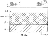
Fig. 9 (a) and (b) are the figure in the semiconductor device manufacturing engineering of the 3rd execution mode, and it is to amplify the fragmentary cross-sectional view that shows and along its distribution map of section boron concentration in engineering shown in Fig. 4 (a), with the structure in emitter base interface.
Figure 10 is the profile that shows existing HBT structure.
Figure 11 (a) and (b) show existing bipolar transistor and the base current of the HBT of the present invention that forms by the 3rd execution mode, collector current to the interdependence of base-emitter voltage.
Figure 12 (a) and (b) are to show the fragmentary cross-sectional view that amplifies in existing HBT emitter base interface and along near the CONCENTRATION DISTRIBUTION of the section boron emitter base interface.
Figure 13 is the profile of demonstration as the bipolar transistor structure of the semiconductor device of basic structure variation of the present invention.
Embodiment
Fig. 1 is the profile of the basic SiGe-HBT structure of demonstration the present invention.
As shown in the drawing, import N type impurity such as phosphorus with methods such as epitaxial growth methods, ion implantation on the top that with (001) face is the Si substrate 100 of interarea, constitute the reverse trap 101 that contains N type impurity of dark 1 μ m.The concentration of N type impurity is adjusted at 1 * 10 in the Si substrate 100 near surface zones
17Atomscm
-3About.Also have, be provided with by the shallow ridges 103 of silica landfill with by undoped polycrystalline silicon film 105 and surround the zanjon 104 that its silicon oxide film 106 constitutes for element separation.The degree of depth of groove 103,104 is respectively about 0.35 μ m, 2 μ m.
Be provided with collector layer 102 in the zone of in Si substrate 100, being seized on both sides by the arms, be provided with N in the zone that in Si substrate 100, isolates with collector layer 102 by shallow ridges 103 by groove 103
+Collector electrode is drawn layer 107, N
+Collector electrode is drawn layer and is contacted with the electrode of collector layer 102 by reverse trap 101.
Also have, on Si substrate 100, be provided with the 1st of thick about 30nm and pile up oxide-film the 108, the 1st accumulation oxide-film 108 and have collector electrode peristome 110, on Si substrate 100, be exposed on the part of collector electrode peristome 110, be provided with by the thick about 80nmSi of doping p type impurity
1-XGe
XThe Si/Si that the Si film layer-by-layer growth of layer and thick about 40nm forms
1-XGe
XLayer 111.This Si/Si
1-XGe
XGrowth forms layer 111 by selecting, it only is formed on the part that is exposed to collector electrode peristome 110 in the Si substrate 100.And, Si/Si
1-XGe
XThe function of internal base 119 is played in the bottom of the central portion of layer 111 (back is with the lower zone of the base stage peristome 118 of narration).Si/Si in addition,
1-XGe
XThe function of emitter layer is played on the top of layer 111 central portion.Si/Si
1-XGe
XThe detailed structure of layer 111 will be narrated in the back.In addition, at Si/Si
1-XGe
XInject by the ion of boron on the layer 111 and the surface element of reverse trap 101 and forms extrinsic base injection region Rii, as the part of extrinsic base injection zone Rii formation concentration 3 * 10 on the surface element of reverse trap 101
17Atomscm
-3About junction leakage prevent the layer 113.
At Si/Si
1-XGe
XThe corrosion that layer the 111 and the 1st accumulation oxide-film 108 is provided with thick about 30nm stops with the 2nd accumulation oxide-film 112, and the formation base stage engages and uses peristome 114 and base stage peristome 118 on the 2nd accumulation oxide-film 112.And, be provided with the P of thick about 150nm
+Polysilicon layer 115 and the 3rd is piled up oxide-film 117, P
+Polysilicon layer 115 landfill base stages engage with peristome 114 and extend to the 2nd piles up on the oxide-film 112.By described Si/Si
1-XGe
XRemainder and P in the layer 111 except that base stage peristome 118 lower zones
+Polysilicon layer 115 constitutes extrinsic base 116.
P in addition,
+Polysilicon layer 115 and the 3rd is piled up the part of base stage peristome 118 tops that are positioned at the 2nd accumulation oxide-film 112 in the oxide-film 117 by opening, at P
+Form the 4th of thick about 30nm on the side of polysilicon and pile up oxide-film 120, further, on the 4th accumulation oxide-film 120, be provided with the sidewall of forming by thick about 100nm polysilicon 121.And, be provided with N
+Polysilicon layer 129, its landfill base stage peristome 118 also extend on the 3rd accumulation oxide-film 117 N
+Polysilicon layer 129 plays the function of emitter extraction electrode.The described the 4th piles up oxide-film 120 makes P
+Polysilicon layer 115 and N
+Polysilicon layer 129 electric insulations, meanwhile, also stop from P
+Polysilicon layer 115 is to N
+The diffusion of impurities of polysilicon layer 129.In addition, the 3rd accumulation oxide-film 117 makes P
+Top and the N of polysilicon layer 115
+ Polysilicon layer 129 insulation.Further, N
+Polysilicon layer 129 and P
+The lateral surface of polysilicon layer 115 is covered by sidewall 123.
Further, draw layer 107, P at collector electrode
+Polysilicon layer 115 and N
+Form Ti silicide layer 124 on the surface of polysilicon layer 129 respectively.
In addition, all by 125 coverings of interlayer dielectric film, perforation interlayer dielectric 125 forms arrival N respectively to substrate
+Collector electrode is drawn the P of layer 107, an extrinsic base part
+The N of polysilicon layer 115 and emitter extraction electrode
+Connecting hole on the Ti silicide layer 124 on the polysilicon layer 129.And, be provided with the W plug 126 of each connecting hole of landfill and be connected with each W plug 126 and extend to metal line 127 on the interlayer dielectric 125.
Here, Fig. 2 (a) and (b) are profiles that the emitter base interface part among Fig. 1 is amplified and along near the CONCENTRATION DISTRIBUTION of the section boron emitter base junction.Shown in Fig. 2 (a), Si/Si
1-XGe
X Layer 111 order lamination are provided with the SiGe laying 151 of Ge content 15%, unadulterated thick about 40nm, and lower end Ge content 15%, upper end be 0 almost continually varying, contain concentration is 4 * 10
18Atomscm
-3Boron, thickness is inclination SiGe base layer 152 and the Si cap rock 153 part doped with boron, thick about 40nm of 40nm.And, in Si cap rock 153 with N
+On the zone that polysilicon layer 129 (emitter extraction electrode) joins by N
+The N type that the diffuses to form emitter diffusion layer 153a of polysilicon layer 129 high concentration phosphorus.The CONCENTRATION DISTRIBUTION of Doping Phosphorus, phosphorus is that depth direction along substrate is from 1 * 10 on emitter diffusion layer 153a
20Atomscm
-3To 1 * 10
17Atomscm
-3About.
Also have, being doped with concentration as the top of Fig. 2 (b) Si cap rock 153 that is shown in is 1 * 10
18Atomscm
-3Boron, in the bottom of Si cap rock 153 owing to concentration about 2 * 10 is arranged from the diffusing, doping of inclination SiGe base layer 152
18Atomscm
-3Boron.On the other hand, the mid portion at Si cap rock 153 does not almost have doped with boron.And, at emitter diffusion layer 153a and surround between its peripheral tier 153b and form PN junction, and between the 1st depletion layer end that in the 1st depletion layer end to the 2 depletion layer end scopes, forms depletion layer 154, depletion layer 154 and the 2nd depletion layer end, seizing its study of the Chinese classic PN junction face of controlling down on both sides by the arms.At this moment, compare to a central lateral deviation with the shape of existing HBT depletion layer 554 (with reference to Figure 12 (a)) near the 2nd shape of piling up oxide-film 112 parts in the depletion layer 154 and move.
Like this, adopt SiGe-HBT of the present invention, shown in Fig. 2 (a), because at the boron of the top of Si cap rock 153 (the 2nd pile up oxide-film 112 under to the zone) high concentration of having mixed, the width of depletion layer 154 (from the distance of the 1st depletion layer end to the 2 depletion layer ends), particularly in the reduced width of Si cap rock 153 top depletion layers.Consequently charge carrier diffusion in depletion layer 154, compound amount reduce, and recombination current reduces.
Figure 11 (b) illustrates the base current, collector current of the HBT of the present invention that the 3rd execution mode that will narrate with the back the forms dependence (Gummel characteristic) to base-emitter voltage.In the figure, transverse axis represents that base stage is launched voltage (V), the longitudinal axis is represented base current or collector current (A) (logarithm value).As shown in the drawing, keep good parallel relation from the low base current characteristic line and collector current characteristic line of being biased in the very wide zone of high bias voltage, it shows and has obtained the good HBT of the linearity.
Therefore, adopt the present invention, shown in Fig. 2 (a), because the boron of the higher concentration that mixed on the top of Si cap rock 153 can suppress the expansion of depletion layer.Consequently can suppress to improve (Gummel characteristic), thereby can access the good HBT of the linearity because of the compound recombination current that causes of charge carrier in depletion layer.
Also have, may reduce the interface energy level at the interface of piling up oxide-film 112 in Si cap rock 153 upper ends and the 2nd because boron is doped with, the minimizing of interface energy level also can contribute to the linearity of improving HBT.In homogeneity Si bipolar transistor, the annealing of carrying out the heat treatment (for example 900 ℃) under the higher temperature can be easy to reduce the 2nd interface energy level of piling up oxide-film 112 and Si cap rock 153, but, in SiGe-HBT, owing to be difficult to carry out the high-temperature heat treatment of needs, mix with boron and realize that reducing interface energy level is a kind of desirable method.And, just can reduce recombination probability U in the following formula owing to reduced interface energy level density, just can further reduce recombination current.
In addition, we show the representative value of above-mentioned each layer thickness, can select suitable thickness for use according to kind and the purposes of HBT.
Below, just with for each relevant execution mode of the manufacture method that realizes structure shown in Fig. 1, Fig. 2 (a) describe.
The 1st execution mode
At first, with reference to Fig. 3 (a)~Fig. 6 (b) basic procedure of HBT manufacturing engineering in the 1st execution mode is described.
At first, be engineering shown in Fig. 3 (a), at (001) face is the top doped N-type impurity one side epitaxial growth Si single crystalline layer of the Si substrate 100 of interarea, perhaps injects the reverse trap of N type (retrograde well) 101 that forms dark about 1 μ m at the laggard capable energetic ion of epitaxial growth.But, also can not carry out epitaxial growth, on the part of Si substrate 100, carry out ion and inject to form reverse trap 101.At this moment, since Si substrate 100 near surface zones will become HBT collector layer, the concentration of its N type impurity is adjusted to 1 * 10 in advance
17Atomscm
-3About.
Secondly, for element separation, form the shallow ridges 103 and the zanjon 104 of landfill silica, zanjon 104 is made of undoped polycrystalline silicon film 105 and the silicon oxide film 106 that surrounds it.The degree of depth of each groove 103,104 is respectively about 0.35 μ m and 2 μ m.In Si substrate 100, just become collector layer 102 by the zone of seizing on both sides by the arms between the shallow ridges 103.Also have, Si substrate 100 in by in shallow ridges 103 and collector layer 102 isolation regional, the N that contacts with collector electrode of formation
+Collector electrode is drawn layer 107.
Then, adopt the manufacture method of standard, form each gate insulating film, gate electrode, source, drain region of each MISFET basic structure of cmos device etc., these processes are not shown.
Once more, it is engineering shown in Fig. 3 (b), under 680 ℃, carry out chemical vapor-phase growing (CVD), on wafer, form the 1st of thick about 30nm and pile up oxide-film 108 with tetraethoxysilane (TEOS) and oxygen, then, pile up the formation width collector electrode peristome 110 wideer on the oxide-film 108 the 1st than active area with the wet etching of fluoric acid etc.That is to say, because that the collector electrode peristome 110 that forms has comprised the width of border, collector electrode peristome 110 of shallow ridges 103 and Si substrate 100 surface elements is wideer than the width of active area.The width of collector electrode peristome 110 self is identical with the cardinal principle of existing HBT, but since two shallow ridges 103 at interval than having the narrow of HBT now, consequently the width of collector electrode peristome 110 is just wide than the width of active area.
Once more, with the part that the mixed liquor treatment S i substrate 100 of ammoniacal liquor and aquae hydrogenii dioxidi is exposed in the collector electrode peristome 110, go up the protection oxide-film that forms thick about 1nm in this section, wafer is put into the chamber of UHV-CVD device with this state.And heat-treat in nitrogen atmosphere and remove the protection oxide-film putting into the back, then, under 550 ℃ temperature, suitably utilize to contain disilane (Si
2H
6), germane (GeH
4), adulterant diborane (B
2H
6) gas that waits, be exposed on the surface of collector electrode peristome 110 parts at Si substrate 100 with the method for each execution mode of narrating later, the Si of the thick about 80nm of epitaxial growth
1-XGe
XLayer.And forming Si
1-XGe
XLayer back, in the indoor gas of feeding chamber continuously, stop to supply with germane, suitably utilize diborane in addition, in Si substrate 100 at Si
1-XGe
XThe Si layer of the thick about 40nm of epitaxial growth on the layer is by Si
1-XGe
XLayer and Si layer form Si/Si
1-XGe
XLayer 111.
Once more, be the engineering shown in Fig. 4 (a), on wafer, form the 2nd of thickness 30nm and pile up oxide-film 112 formation corrosion stopper films, then, using the resist mask Rel that is located on the 2nd accumulation oxide-film 112 that the 2nd accumulation oxide-film 112 is carried out dry etching makes it graphically, forms base stage joint peristome 114.At this moment, Si/Si
1-XGe
XThe central portion of layer 111 is piled up oxide-film by the 2nd and is covered, and engages with peristome 114 Si/Si of place in base stage
1-XGe
XThe periphery of layer 111 and the 1st part of piling up oxide-film 108 come out.Secondly, be used in the ion injection formation leap Si/Si that carries out boron (B) p type impurity of etc.ing when forming base stage and engaging with the resist mask Rel that crosses with peristome 114
1-XGe
XThe extrinsic base injection region Rii of layer 111 and reverse trap 101 surface portions.At this moment, as the part of extrinsic base injection zone Rii, having formed concentration on the surface element of reverse trap 101 is 3 * 10
17Atomscm
-3Junction leakage prevent the layer 113.
Once more, be the engineering shown in Fig. 4 (b), on wafer, pile up 1 * 10 with the CVD method
20Atomscm
-3The P of above high-concentration dopant, thick about 150nm
+Polysilicon layer 115 is followed, is piled up the 3rd of thick about 100nm and piles up oxide-film 117.Secondly, pile up oxide-film 117 and P with the dry etching method with the 3rd
+Polysilicon layer 115 is graphical, piles up oxide-film 117 and P the 3rd
+Form the base stage peristome 118 that arrives the 2nd accumulation oxide-film 112 on the central portion of polysilicon layer 115.The central portion that this base stage peristome 118 to the 2 is piled up oxide-film 112 is little, base stage peristome 118 does not stride across base stage and engages with peristome 114.Form by P by this project
+Polysilicon layer 115 and Si/Si
1-XGe
XThe extrinsic base 116 that the remainder of layer 111 except that central portion constitutes.
Once more, be the engineering shown in Fig. 5 (a), on whole of wafer, pile up the accumulation oxide-film of thick about 30nm and the polysilicon film of thick about 150nm with the CVD method.And, will pile up the corrosion of oxide-film and polysilicon film with anisotropic dry etch, at P
+Formation sidewall 121, sidewall 121 are formed by seizing the 4th polysilicon of piling up oxide-film 120 on both sides by the arms on the side of polysilicon layer 115 and the 3rd accumulation oxide-film 117.Secondly, carry out wet etching with fluoric acid etc., removing the 2nd piles up oxide-film 112 and the 4th and piles up exposed portions in the oxide-film 120.At this moment, in base stage peristome 118, Si/Si
1-XGe
XThe Si layer on layer 111 top comes out.Also have, because wet etching is an isotropic etch, the 2nd piles up oxide-film 112 and the 4th and pile up oxide-film 120 and laterally also be corroded, the size of base stage peristome 118 has just enlarged.That is to say, by the width of the amount decision base stage opening of wet etching at this moment.Even when this wet etching, on the 1st accumulation oxide-film 108, paying SiGe island 111, because N in the Si substrate 100
+Collector electrode is drawn layer 107 grade by P
+Do not come out in the surface of coverings such as polysilicon layer 115, Si substrate 100.
Once more, be the engineering shown in Fig. 5 (b), pile up the N of thick about 250nm
+Polysilicon layer 129 backs, usefulness dry etching method are with N
+Polysilicon layer 129 graphical, formation emitter extraction electrodes.At this moment, because P
+The outside of polysilicon layer 115 does not form the sidewall of being made up of polysilicon not by graphically on the side.In addition, because N
+Collector electrode is drawn the surface of layer 107 grade not because of N
+The excessive erosion of polysilicon 129 and being corroded is not so form concavo-convex on the surface of Si substrate 100 yet.
Once more, be engineering shown in Fig. 6 (a), pile up oxide-film 117, P with dry etching with the 3rd
+It is graphical that polysilicon layer 115 and the 2nd is piled up oxide-film 112, thus the shape of decision extrinsic base 116.
Be the engineering shown in Fig. 6 (b), behind the accumulation oxide-film that forms thick about 120nm on the wafer, carry out dry etching, once more, at N
+Polysilicon layer 129 and P
+Form sidewall 123 on the side of polysilicon layer 115.By dry etching (excessive erosion) at this moment the part that the 1st accumulation oxide-film 108 exposes is removed, make N
+Polysilicon layer 129, P
+Polysilicon layer 115 and N
+Collector electrode is drawn the surface of layer 107 and is come out.
Further, for to obtain structure shown in Figure 1, carry out following processing.At first, on whole of wafer, pile up the Ti film of thick about 40nm, carry out 675 ℃, 30 seconds RTA (short annealing), thus at N with sputtering method
+Polysilicon layer 129, P
+Polysilicon layer 115 and N
+Collector electrode is drawn on the surface of layer 107 expose portion and is formed Ti silicide layer 124.After then, optionally only removing Ti film non-reacted parts, annealing changes the crystal structure of Ti silicide layer 124.
Once more, on whole of wafer, form interlayer dielectric 125, connect interlayer dielectric 125 and form and arrive N
+Polysilicon layer 129, P
+Polysilicon layer 115 and N
+Collector electrode is drawn the connecting hole of the Ti silicide layer 124 on the layer 107.And, with after forming W plug 126 in each connecting hole of W film landfill, on whole of wafer, pile up aluminium alloy film, aluminium alloy film is graphical, form and be connected with each W plug 126 and extend to metal line 127 on the interlayer dielectric 125.
By above engineering, just formed HBT with structure shown in Figure 1, in other words, formed have the collector electrode formed by N type Si, by P
+Type Si
1-XGe
XThe base stage of forming and by N
+The HBT of the emitter that type Si forms.Si/Si in addition,
1-XGe
XSi layer in the layer 111 is because from N
+The diffusion of the high concentration N type impurity (phosphorus etc.) of polysilicon layer 129 becomes and is N
+Type Si layer.
Once more, just has the Si/Si of characteristics in the present embodiment with reference to Fig. 7 (a) and (b)
1-XGe
XThe formation engineering of layer 111 is done an explanation.Fig. 7 (a) and (b) are fragmentary cross-sectional views that the structure in the emitter base interface of engineering shown in Fig. 3 (b) in the described manufacturing engineering is amplified and along the concentration profile of its section boron.
At first, the part with the mixed liquor treatment S i substrate 100 of ammoniacal liquor and aquae hydrogenii dioxidi is exposed in the collector electrode peristome goes up the protection oxide-film that forms about thick about 1nm in this section, wafer is sent in the chamber of UHV-CVD device in this state.And, wafer is being sent in the chamber back, under vacuum atmosphere with wafer 850 ℃ of heating 2 minutes down, remove protective oxide film.Secondly, in chamber, make chip temperature drop to 550 ℃, disilane (Si
2H
6) and germane (GeH
4) flow be respectively 0.02l/min and 0.03l/min, pressure are 0.067Pa, kept in this state 2 minutes and 40 seconds, on wafer, form the not doping SiGe laying 151 of thick about 40nm.At this moment, the speed of growth of SiGe laying 151 is about 15nm/min.
Then, continue to keep chamber interior temperature, pressure and disilane (Si
2H
6) flow, with the hydrogen of concentration 5% dilution diborane (B
2H
6) indoor with flow 4sccm introduction chamber.And in 4 minutes, make germane (GeH
4) flow vary continuously to 0l/min, the inclination SiGe base layer 152 of the about 40nm of epitaxial growth thickness, mixed crystal Si from 0.03l/min
1-XGe
XIn Ge content X change to 0% from 15%.At this moment, the average speed of growth of inclination SiGe base layer 152 is that the concentration of 10nm/min, boron is about 4 * 10
18Atomscm
-3
Once more, keep chamber interior temperature, pressure and disilane (Si
2H
6) flow constant, germane (GeH does not circulate
4), stop hydrogen dilution diborane (B
2H
6) supply, kept the not doping Si layer 161 of the thick about 30nm of epitaxial growth in this state 15 minutes.At this moment, the do not mix speed of growth of Si layer 161 is about 2nm/min.
Then, again with in chamber, the circulate hydrogen dilution diborane (B of concentration 5% of flow 0.001l/min
2H
6), kept this state 5 minutes, the doping Si layer 162 of the thick about 10nm of epitaxial growth.At this moment, the speed of growth of doping Si layer 162 is about 2nm/min, boron concentration is about 1 * 10
18Atomcm
-3
After described engineering is finished, Si layer 161 and doping Si layer 162 do not form Si cap rock 153 by mixing.Also have, by at the bottom of the SiGe liner 151, inclination SiGe base layer 152 and Si cap rock 153 form Si/Si
1-XGe
XLayer 111.
Fig. 7 (b) is illustrated in Si/Si
1-XGe
XLayer 111 has just formed the distribution map of the preceding boron concentration of after-baking.Under this state, only the doping Si layer 162 in inclination SiGe base layer 152 and Si cap rock 153 presents the steep concentration profile that high concentration boron exists.
And, owing to later on have heat treatment to add in each engineering, the boron diffusion of mixing in the doping Si layer 162 in inclination SiGe base layer 152 and Si cap rock 153 finally obtains the boron concentration profile shown in Fig. 2 (b).
Doped with boron in the present embodiment, when the Si cap rock forms, its feature are to be mixed by in-situ to carry out CVD.And, owing to adopt in-situ to mix in the present embodiment, can be controlled at the boron concentration of mixing in Si cap rock 153 tops with degree of precision.
The 2nd execution mode
In the present embodiment, shown the same of Fig. 2 (a)~Fig. 6 (b) of illustrating in the flow process of basic HBT manufacturing engineering and the 1st execution mode.
In the present embodiment, it is characterized in that: engineering is carried out by the following method shown in Fig. 4 (a).Fig. 8 (a) and (b) are with the fragmentary cross-sectional view that the emitter base junction plot structure amplifies in the engineering shown in Fig. 4 (a) in the described manufacturing engineering and along its concentration profile of section boron.
In the present embodiment, handle by the method that has illustrated in the 1st execution mode, the not doping SiGe laying 151 and the thick about 40nm boron concentration that form thick about 40nm on collector layer 102 are about 4 * 10
18Atomscm
-3Inclination SiGe base layer 152.
Secondly, keep chamber interior temperature, pressure and disilane (Si
2H
6) flow and inclination SiGe base layer 152 the same when forming, germane (GeH no longer circulates
4), stop hydrogen dilution diborane (B
2H
6) supply, this state was kept 20 minutes the Si cap rock 153 of the thick about 40nm of epitaxial growth.
Once more, replace the 2nd in the 1st execution mode to pile up oxide-film 112, on Si cap rock 153, pile up the 2nd accumulation oxide-film of forming by boron doped silicon oxide film (bsg film) 171.At this moment, in the chamber of atmospheric pressure cvd device, wafer is warmed up to 400 ℃ after, under normal pressure, feeding flow is the tetraethoxysilane (TEOS) of 1.5l/min, the triethoxy-boron (TEB) that flow is 1.5l/min, the 85g/Nm that contains that flow is 7.5l/min
3The O of concentration ozone
2, flow is the N of 18.0l/min
2, kept this state 15 seconds, formation contains the 2nd accumulation oxide-film 171 3wt% boron, thick about 30nm.
Fig. 8 (b) is the concentration profile that shows boron on the vertical section in this case.Though do not have doped with boron in the Si cap rock 153 under this state,, final obtain the boron concentration profile shown in Fig. 2 (a) because the heat treatment, the 2nd of back in the engineering is piled up boron diffusion in the oxide-film 171 to the top of Si cap rock 153.
Then, the same with engineering shown in Fig. 4 (a), pile up the 2nd and to form base stage on the oxide-film 171 and connect with peristome 114, carry out engineering shown in Fig. 4 (b)~Fig. 6 (b), the HBT that obtains having structure shown in Figure 1.
Certainly, the 2nd accumulation oxide-film 171 should use psg film in the PNP bipolar transistor.
Adopt present embodiment, the enough fairly simple engineerings of energy doped with boron in Si cap rock 153.Particularly it might reduce in the upper end of Si cap rock 153 and piles up oxide-film 112 interface energy level at the interface with the 2nd.
The 3rd execution mode
In the present embodiment flow process of basic HBT manufacturing engineering also with the 1st execution mode in illustrated with the same shown in Fig. 2 (a)~Fig. 6 (b).
Characteristics in the present embodiment are that the engineering shown in Fig. 4 (a) and (b) is carried out by the following method.Fig. 9 (a) and (b) illustrate the fragmentary cross-sectional view of the amplification of the emitter base junction plot structure shown in Fig. 4 (a) and (b) in the described manufacturing engineering, reach the concentration profile along section boron.
In the present embodiment, carry out the same processing with the 1st execution mode explanation, on collector layer 102, form the not doping SiGe laying 151 of thick about 40nm, thick about 40nm contains concentration 4 * 10
18Atomscm
-3The inclination SiGe base layer 152 of boron.
Secondly, keep chamber interior temperature, pressure and disilane (Si
2H
6) flow the same when forming inclination SiGe base layer 152, germane (GeH does not circulate
4), stop hydrogen dilution diborane (B
2H
6) supply, this state was kept 20 minutes the Si cap rock 153 of the thick about 40nm of epitaxial growth.
Once more, carry out and the processing much at one of the 1st execution mode formation the 2nd accumulation oxide-film 112 formation etch stop layers on wafer.At this moment, the 2nd thickness of piling up oxide-film 112 is 10nm in the present embodiment.
Once more, adopt the processing that illustrate in the 1st execution mode, connect with peristome 114 by the 2nd graphical base stage that forms of piling up oxide-film 112, be used in that used resist mask carries out the injection of boron (B) ion when forming the base stage connection with peristome 114.
Such, the usefulness CVD method that once more, illustrated in the engineering shown in Fig. 4 (b) piled up the P of thick about 150nm on wafer
+Polysilicon layer 115, P in the present embodiment
+The concentration of boron is greater than 2 * 10 in the polysilicon 115
20Atomscm
-3This boron concentration can be after piling up the undoped polycrystalline silicon film, at the about 8keV of accelerating voltage, dosage about 5 * 10
15Atoms scm
-2Condition under on polysilicon film, carry out the boron ion and inject to realize.But, also can when polysilicon film is piled up, carry out in-situ and mix.Then, carry out the processing same, pile up the 3rd accumulation silicon oxide film 117 (with reference to Fig. 4 (b)), by the 3rd accumulation oxide-film 117 and P with the 1st execution mode
+Graphical and then the formation base stage peristome 118 of polysilicon layer 115 forms by P
+Polysilicon layer 115 and remove Si/Si
1-XGe
XThe outer other parts of layer 111 central portion constitute extrinsic base 116 (with reference to Fig. 4 (b)).
Fig. 9 (b) illustrates the concentration profile of this moment along vertical section boron.Though in Si cap rock 153, do not have doped with boron in this state, only piled up the P that oxide-film 112 separates by the 2nd
+The high concentration boron that mixed in the polysilicon layer 115 (part of extrinsic base layer 116), but because heat treatment, the P of engineering later on
+Boron in the polysilicon layer 115 is piled up the top that oxide-film 112 is diffused into Si cap rock 153 by the 2nd, finally obtains the boron concentration profile shown in Fig. 2 (a).
Then, carry out the engineering shown in Fig. 5 (a)~Fig. 6 (b), the HBT that obtains having Fig. 1 structure.
Adopt present embodiment, owing to be under the state that has formed base stage peristome 118 from P
+Polysilicon layer 115 is to the top of Si cap rock 153 doped with boron, thereby can be only under base stage peristome 118 in Si cap rock 153 importing of the zone zone boron, and the emitter diffusion layer 115a just of the zone under the base stage peristome 118, like this, just do not need to consider with emitter diffusion layer 153a in the concentration relationship of Doping Phosphorus.Therefore, the concentration of Si cap rock 153 top boron can be adjusted to optimal concentration, this is its advantage.
Other execution modes
In the respective embodiments described above, we are applicable to that with regard to the present invention the situation of dual poly type HBT is described, still, the present invention is not limited in such execution mode, the 1st, the 2nd execution mode also is applicable to single polysilicon type HBT.During the sort of situation, do not establish N
+Polysilicon layer 115 adopts Si/Si
1-XGe
XLayer 111 extends to the 1st structure of piling up on the oxide-film 108, removes just passable with surrounding base stage peristome 118 parts part in addition in the 2nd accumulation oxide-film 112.At this moment Si/Si
1-XGe
XIt is not monocrystalline and adopt polycrystalline structure that layer 111 meta are piled up part on the oxide-film 108 the 1st, because this part is the part, simple just passable as the function of resistance as the extrinsic base function, and work and characteristic as HBT are not exerted an adverse impact.
Shown in Fig. 2 (b), to the bottom of Si cap rock 153 doped with boron, in each execution mode, also can mix to the bottom of Si cap rock 153 doped with boron by in-situ by diffusion.
In addition, in described each execution mode, though be to be that example illustrates with NPN type HBT, the present invention also is adapted to the HBT of positive-negative-positive certainly.During the sort of situation, the conduction type of HBT each several part, the conduction type of HBT each several part impurity need adopt and the opposite conduction type of described each execution mode.
Also have, SiGe-HBT of the present invention and Si-CMOS FET can be formed on the same Si substrate, can access so-called BiCMOS device.
Replace SiGe laying, inclination SiGe base layer in described each execution mode that SiGeC laying, inclination SiGeC base layer also can be set.
Si/Si in the 1st~the 3rd execution mode
1-XGe
XLayer 111 also can extend to the 1st and pile up on the oxide-film 108.
The variation of structure
In the structure shown in Figure 1, use Si
1-XGe
X(0≤X<1=constitutes base layer to layer, also can use Si
1-X-yGe
XC
yLayer (0≤x, y<1=and Si
1-yC
y(0≤y<1=replaces Si to layer
1-XGe
XLayer constitutes base layer.Also have, some at least in the emitter and collector also can be by Si
1-XGe
XLayer, Si
1-X-yGe
XC
yLayer or Si
1-yC
yLayer constitutes.
Figure 13 is and uses Si
1-X-yGe
XC
yLayer replaces the Si in the basic structure
1-XGe
XThe profile of the heterojunction bipolar transistor (HBT) that layer variation is relevant.In this variation the HBT structure shown in the structure of HBT and described Fig. 1 much at one, only in following some difference.
Be exposed to the Si that is provided with on the part of collector electrode peristome 110 by doping p type impurity, thick about 80nm on Si substrate 100
1-X-yGe
XC
yThe Si/Si that the Si film lamination of layer and thick about 40nm forms
1-X-yGe
XC
yLayer 211.This Si/Si
1-X-yGe
XC
yLayer 211 usefulness select growth method only to be formed on the part that is exposed to collector electrode peristome 110 in the Si substrate 100.And, Si/Si
1-X-yGe
XC
yThe function of internal base 219 is played in the bottom of the central portion (lower zone of the base stage peristome of narrating later 118) of layer 211.Si/Si in addition,
1-XGe
XC
yThe function of emitter layer is played on the top of layer 211 central portion.Si/Si
1-XGe
XC
yThe detailed structure of layer 211 can be suitable for the such impurity profile of the 1st~the 3rd execution mode that has illustrated.Also have, form with the boron ion implantation and cross over Si/Si
1-XGe
XC
yThe extrinsic base injection region Rii of layer 211 and reverse trap 101 surface elements.At Si/Si
1-XGe
XC
yLayer the 211 and the 1st is piled up corrosion that oxide-film 108 is provided with thick about 30nm and is stopped to pile up oxide-film 112 with the 2nd, piles up the 2nd to form base stage connection peristome 114 and base stage peristome 118 on the oxide-film 112.And, be provided with the landfill base stage and connect with peristome 114 and extend to the P of the thick about 150nm on the 2nd accumulation oxide-film 112
+Polysilicon layer 115 and the 3rd is piled up oxide-film 117.By described Si/Si
1-XGe
XC
yRemove the part and the P of base stage peristome 118 lower zones in the layer 211
+Polysilicon layer 115 constitutes extrinsic base 216.
Miscellaneous part shown in Figure 13 is paid with the symbol identical with Fig. 1, is omitted explanation because of identical with structure shown in Figure 1.Si in the manufacturing engineering, in replacement the 1st~the 3rd execution mode
1-XGe
XLayer epitaxially grown, carry out Si/Si
1-X-yGe
XC
yThe epitaxial growth of layer.
Semiconductor device of the present invention is applied to carrying the devices such as bipolar transistor on e-machine, particularly is applied to handle the device of high-frequency signal.
Claims (9)
1. (modification) a kind of bipolar transistor, it possesses: the 1st semiconductor layer, the 2nd semiconductor layer, the 3rd semiconductor layer, dielectric film, peristome and emitter extraction electrode;
Described the 1st semiconductor layer is located on the substrate, contains the 1st conductive-type impurity, constitutes collector layer,
Described the 2nd semiconductor layer is located on described the 1st semiconductor layer, contains the 2nd conductive-type impurity, constitutes base layer,
Described the 3rd semiconductor layer is located on described the 2nd semiconductor layer, is made up of the material different with described the 2nd semiconductor layer energy gap,
Described dielectric film is arranged on described the 3rd semiconductor layer, and peristome is arranged on the described dielectric film and arrives described the 3rd semiconductor layer,
The emitter extraction electrode by conductor material constitute, the described dielectric film peristome of landfill and contact with described the 3rd semiconductor layer;
Described the 3rd semiconductor layer has the 1st conductivity type emitter diffusion layer that is positioned at described peristome below and the peripheral tier that is positioned at this zone, emitter diffusion layer side,
Described peripheral tier comprises the 2nd conductive-type impurity,
Be included in the 2nd conductive-type impurity of described peripheral tier, be high concentration, be low concentration, be the inside that the mode of high concentration is distributed in described peripheral tier in the bottom of described peripheral tier at the central portion of described peripheral tier with top in described peripheral tier.
2. bipolar transistor according to claim 1, it is characterized in that:
Described dielectric film is made of the silicon oxide film that is doped with the 2nd conductive-type impurity,
The 2nd conductive-type impurity that comprises at least a portion in described the 3rd semiconductor layer top obtains from described dielectric film diffusion.
(modification) bipolar transistor according to claim 1, it is characterized in that:
This bipolar transistor also possesses polysilicon film, it be connected with the part that is positioned at dielectric film foreign side described in described the 3rd semiconductor layer and, it is provided with to such an extent that extend on the described dielectric film, be doped with the 2nd conductive-type impurity, play the function of base stage extraction electrode.
At least the 2nd conductive-type impurity that contains on the part on described the 3rd semiconductor layer top obtains by described dielectric film diffusion from described polysilicon film.
(modification) it is characterized in that according to the described bipolar transistor of claim 1:
The 1st conductive-type impurity in the emitter diffusion layer of described the 3rd semiconductor layer obtains from described emitter extraction electrode diffusion.
(modification) it is characterized in that according to the described bipolar transistor of claim 1:
Described substrate is a silicon substrate,
Described the 1st semiconductor layer is the Si layer,
Described the 2nd semiconductor layer is SiGe layer or SiGeC layer,
Described the 3rd semiconductor layer is the Si layer.
6. the manufacture method of (modification) a kind of bipolar transistor, it comprises following engineering:
(a) engineering of formation the 2nd semiconductor layer on the 1st semiconductor layer, the 1st semiconductor layer is located on the substrate, contains the 1st conductive-type impurity, constitutes collector layer, and the 2nd semiconductor layer contains the 2nd conductive-type impurity, constitutes base layer;
(b) form the engineering of the 3rd semiconductor layer with epitaxial growth method on described the 2nd semiconductor layer, the 3rd semiconductor layer is constituted, is contained the 2nd conductive-type impurity on its top at least by the material different with described the 2nd semiconductor layer energy gap;
(c) engineering back in described engineering (b), accumulation dielectric film on substrate;
(d) on described dielectric film, form the engineering that arrives described the 3rd semiconductor layer peristome;
(e) in described the 3rd semiconductor layer, be positioned at zone below the described peristome, import the 1st conductive-type impurity, form the engineering of emitter diffusion layer,
By described engineering (c) processing afterwards, the 2nd conductive-type impurity that mixes in the side of emitter diffusion layer described in described the 3rd semiconductor layer, and form peripheral tier,
Be included in the 2nd conductive-type impurity of described peripheral tier, be high concentration, be low concentration, be the inside that the mode of high concentration is distributed in described peripheral tier in the bottom of described peripheral tier at the central portion of described peripheral tier with top in described peripheral tier.
7. the manufacture method of (modification) a kind of bipolar transistor is characterized in that:
It comprises following engineering:
(a) engineering of formation the 2nd semiconductor layer on the 1st semiconductor layer, the 1st semiconductor layer is located on the substrate, comprises the 1st conductive-type impurity, constitutes collector layer, and the 2nd semiconductor layer contains the 2nd conductive-type impurity, constitutes base layer;
(b) form the engineering of the 3rd semiconductor layer with epitaxial growth method on described the 2nd semiconductor layer, the 3rd semiconductor layer is made up of the material different with described the 2nd semiconductor layer energy gap;
(c) in described engineering (b) back, on substrate, pile up the engineering that contains the 2nd conductive-type impurity dielectric film;
(d) on described dielectric film, form the engineering that arrives described the 3rd semiconductor layer peristome;
(e) in described the 3rd semiconductor layer, be positioned at zone below the described peristome, import the engineering of the 1st conductive-type impurity formation emitter diffusion layer;
By the processing after the described engineering (c), from described dielectric film the 2nd conductive-type impurity that mixes on the top of described the 3rd semiconductor layer, form peripheral tier in the side of described emitter diffusion layer,
Be included in the 2nd conductive-type impurity of described peripheral tier, be high concentration, be low concentration, be the inside that the mode of high concentration is distributed in described peripheral tier in the bottom of described peripheral tier at the central portion of described peripheral tier with top in described peripheral tier.
8. the manufacture method of (modification) a kind of bipolar transistor is characterized in that:
It comprises following engineering:
(a) engineering of formation the 2nd semiconductor layer on the 1st semiconductor layer, the 1st semiconductor layer is located on the substrate, comprises the 1st conductive-type impurity, constitutes collector layer, and the 2nd semiconductor layer contains the 2nd conductive-type impurity, constitutes base layer;
(b) form the engineering of the 3rd halfbody conductor layer with epitaxial growth method on described the 2nd semiconductor layer, the 3rd semiconductor layer is made up of the material different with described the 2nd semiconductor layer energy gap;
(c) engineering back in described engineering (b), accumulation dielectric film on substrate;
(d) pile up on the substrate contain the 2nd conductive-type impurity electrically conductive film after, on this electrically conductive film, form the engineering of the peristome that reaches described dielectric film;
The engineering of the sidewall of (e) form to cover the side of described the 1st electrically conductive film peristome, forming by insulating material;
(f) engineering back in described engineering (e), the peristome of described the 3rd semiconductor layer of formation arrival on described dielectric film;
(g) in described the 3rd semiconductor layer, be positioned at the engineering that zone below the described peristome imports the 1st conductive-type impurity, formation emitter diffusion layer;
By the processing after the described engineering (d), by described dielectric film from described conducting film the 2nd conductive-type impurity that mixes on the top of described the 3rd semiconductor layer, form peripheral tier in the side of described emitter diffusion layer,
Be included in the 2nd conductive-type impurity of described peripheral tier, be high concentration, be low concentration, be the inside that the mode of high concentration is distributed in described peripheral tier in the bottom of described peripheral tier at the central portion of described peripheral tier with top in described peripheral tier.
9. bipolar transistor fabrication method according to claim 8 is characterized in that:
This method also is included in described engineering (f) back, (g) is preceding for described engineering, after piling up the electrically conductive film different on the substrate with described electrically conductive film, will this different electrically conductive film graphically, the formation described dielectric film peristome of landfill and extend on the described dielectric film, contain the engineering of the emitter extraction electrode of the 1st conductive-type impurity.
Applications Claiming Priority (3)
| Application Number | Priority Date | Filing Date | Title |
|---|---|---|---|
| JP2000151044A JP2001332563A (en) | 2000-05-23 | 2000-05-23 | Bipolar transistor and its manufacturing method |
| JP151044/00 | 2000-05-23 | ||
| JP151044/2000 | 2000-05-23 |
Publications (2)
| Publication Number | Publication Date |
|---|---|
| CN1398432A CN1398432A (en) | 2003-02-19 |
| CN1224109C true CN1224109C (en) | 2005-10-19 |
Family
ID=18656664
Family Applications (1)
| Application Number | Title | Priority Date | Filing Date |
|---|---|---|---|
| CNB018013724A Expired - Fee Related CN1224109C (en) | 2000-05-23 | 2001-05-23 | Bipolar transistor and method of manufacture thereof |
Country Status (6)
| Country | Link |
|---|---|
| US (2) | US6828602B2 (en) |
| EP (1) | EP1263052A2 (en) |
| JP (1) | JP2001332563A (en) |
| KR (1) | KR20020019560A (en) |
| CN (1) | CN1224109C (en) |
| WO (1) | WO2001091162A2 (en) |
Families Citing this family (34)
| Publication number | Priority date | Publication date | Assignee | Title |
|---|---|---|---|---|
| DE10160511A1 (en) * | 2001-11-30 | 2003-06-12 | Ihp Gmbh | Bipolar transistor |
| DE10164176B4 (en) * | 2001-12-27 | 2007-12-27 | Austriamicrosystems Ag | bipolar transistor |
| US6670654B2 (en) | 2002-01-09 | 2003-12-30 | International Business Machines Corporation | Silicon germanium heterojunction bipolar transistor with carbon incorporation |
| KR100460201B1 (en) * | 2002-04-08 | 2004-12-08 | 한국전자통신연구원 | Manufacturing method of a virtual substrate for SiGe/Si hetero-junction field-effect transistor |
| JP4391069B2 (en) * | 2002-04-30 | 2009-12-24 | 富士通マイクロエレクトロニクス株式会社 | Hetero bipolar transistor and manufacturing method thereof |
| US6699765B1 (en) | 2002-08-29 | 2004-03-02 | Micrel, Inc. | Method of fabricating a bipolar transistor using selective epitaxially grown SiGe base layer |
| JP2004111852A (en) * | 2002-09-20 | 2004-04-08 | Fujitsu Ltd | Semiconductor device and its manufacture |
| JP3507830B1 (en) | 2002-10-04 | 2004-03-15 | 松下電器産業株式会社 | Semiconductor device |
| JP3643100B2 (en) | 2002-10-04 | 2005-04-27 | 松下電器産業株式会社 | Semiconductor device |
| JP3891299B2 (en) * | 2003-05-06 | 2007-03-14 | セイコーエプソン株式会社 | Semiconductor device manufacturing method, semiconductor device, semiconductor device, electronic device |
| KR100546332B1 (en) * | 2003-06-13 | 2006-01-26 | 삼성전자주식회사 | Bipolar junction transistor and method for fabricating the same |
| US7038298B2 (en) * | 2003-06-24 | 2006-05-02 | International Business Machines Corporation | High fT and fmax bipolar transistor and method of making same |
| US6960820B2 (en) * | 2003-07-01 | 2005-11-01 | International Business Machines Corporation | Bipolar transistor self-alignment with raised extrinsic base extension and methods of forming same |
| US7262484B2 (en) * | 2005-05-09 | 2007-08-28 | International Business Machines Corporation | Structure and method for performance improvement in vertical bipolar transistors |
| US7342293B2 (en) * | 2005-12-05 | 2008-03-11 | International Business Machines Corporation | Bipolar junction transistors (BJTS) with second shallow trench isolation (STI) regions, and methods for forming same |
| US7585740B2 (en) * | 2006-03-14 | 2009-09-08 | International Business Machines Corporation | Fully silicided extrinsic base transistor |
| JP2007250903A (en) | 2006-03-16 | 2007-09-27 | Matsushita Electric Ind Co Ltd | Heterojunction bipolar transistor and manufacturing method therefor |
| US7678667B2 (en) * | 2007-06-20 | 2010-03-16 | Silverbrook Research Pty Ltd | Method of bonding MEMS integrated circuits |
| CN101459076B (en) * | 2007-12-13 | 2011-02-02 | 上海华虹Nec电子有限公司 | Preparation for SiGe HBT transistor |
| CN102064190B (en) * | 2009-11-18 | 2012-07-11 | 上海华虹Nec电子有限公司 | SiGe PNP bipolar transistor in SiGe BiCMOS (Bipolar Complementary Metal Oxide Semiconductor) technique |
| CN102087977B (en) * | 2009-12-04 | 2012-04-18 | 无锡华润上华半导体有限公司 | Vertical negative-positive-negative (NPN) transistor and manufacturing method thereof |
| CN102097465B (en) * | 2009-12-15 | 2012-11-07 | 上海华虹Nec电子有限公司 | Parasitic vertical PNP triode in BiCMOS process and manufacturing method thereof |
| CN102110709B (en) * | 2009-12-24 | 2012-08-01 | 上海华虹Nec电子有限公司 | Parasitic vertical PNP triode in bipolar complementary metal oxide semiconductor (BiCMOS) process and manufacturing method thereof |
| IT1401756B1 (en) | 2010-08-30 | 2013-08-02 | St Microelectronics Srl | INTEGRATED ELECTRONIC DEVICE WITH ON-BOARD TERMINATION STRUCTURE AND ITS MANUFACTURING METHOD. |
| IT1401754B1 (en) | 2010-08-30 | 2013-08-02 | St Microelectronics Srl | INTEGRATED ELECTRONIC DEVICE AND ITS MANUFACTURING METHOD. |
| IT1401755B1 (en) | 2010-08-30 | 2013-08-02 | St Microelectronics Srl | INTEGRATED ELECTRONIC DEVICE WITH VERTICAL CONDUCTION AND ITS MANUFACTURING METHOD. |
| CN102403344B (en) * | 2010-09-10 | 2013-09-11 | 上海华虹Nec电子有限公司 | Parasitic PNP bipolar transistor in silicon germanium BiCMOS (bipolar complementary metal oxide semiconductor) process |
| US8492794B2 (en) * | 2011-03-15 | 2013-07-23 | International Business Machines Corporation | Vertical polysilicon-germanium heterojunction bipolar transistor |
| DE102011108334B4 (en) * | 2011-07-25 | 2016-05-25 | Texas Instruments Deutschland Gmbh | Electronic device and method for increasing the reliability of bipolar transistors under high voltage conditions |
| CN103107087B (en) * | 2011-11-09 | 2015-10-14 | 上海华虹宏力半导体制造有限公司 | The manufacture method of the PNP triode integrated with si-ge heterojunction NPN triode device |
| US8716096B2 (en) | 2011-12-13 | 2014-05-06 | International Business Machines Corporation | Self-aligned emitter-base in advanced BiCMOS technology |
| CN102766908B (en) * | 2012-07-25 | 2016-02-24 | 苏州阿特斯阳光电力科技有限公司 | The Boron diffusion method of crystal silicon solar energy battery |
| US10006365B2 (en) | 2015-06-30 | 2018-06-26 | General Electric Company | Air supply and conditioning system for a gas turbine |
| CN107887430A (en) * | 2017-11-09 | 2018-04-06 | 重庆邮电大学 | Substrate applies the silicon-germanium heterojunction bipolar transistor and its manufacture method of simple stress |
Family Cites Families (16)
| Publication number | Priority date | Publication date | Assignee | Title |
|---|---|---|---|---|
| US4761641A (en) * | 1983-01-21 | 1988-08-02 | Vidcom Rentservice B.V. | Information display system |
| JP2600485B2 (en) * | 1990-11-28 | 1997-04-16 | 日本電気株式会社 | Semiconductor device |
| JPH05102177A (en) * | 1991-10-02 | 1993-04-23 | Hitachi Ltd | Semiconductor integrated circuit device and electronic computer using same |
| JPH05182980A (en) | 1992-01-07 | 1993-07-23 | Toshiba Corp | Heterojunction bipolar transistor |
| JP2582519B2 (en) * | 1992-07-13 | 1997-02-19 | インターナショナル・ビジネス・マシーンズ・コーポレイション | Bipolar transistor and method of manufacturing the same |
| GB9315448D0 (en) * | 1993-07-26 | 1993-09-08 | Rank Xerox Ltd | Recording and retrieval of information relevant to the activities of a user |
| JP2551364B2 (en) * | 1993-11-26 | 1996-11-06 | 日本電気株式会社 | Semiconductor device |
| JP2746225B2 (en) | 1995-10-16 | 1998-05-06 | 日本電気株式会社 | Semiconductor device and manufacturing method thereof |
| EP0818829A1 (en) * | 1996-07-12 | 1998-01-14 | Hitachi, Ltd. | Bipolar transistor and method of fabricating it |
| JPH11102177A (en) | 1997-09-25 | 1999-04-13 | Canon Inc | Font data creation device and method thereof, and storage medium |
| JP3301390B2 (en) | 1998-08-13 | 2002-07-15 | 日本電気株式会社 | Semiconductor device having heterojunction bipolar transistor and method of manufacturing the same |
| US6954859B1 (en) * | 1999-10-08 | 2005-10-11 | Axcess, Inc. | Networked digital security system and methods |
| US20030058111A1 (en) * | 2001-09-27 | 2003-03-27 | Koninklijke Philips Electronics N.V. | Computer vision based elderly care monitoring system |
| US7436887B2 (en) * | 2002-02-06 | 2008-10-14 | Playtex Products, Inc. | Method and apparatus for video frame sequence-based object tracking |
| US20080129495A1 (en) * | 2002-10-28 | 2008-06-05 | Hitt Dale K | Wireless sensor system for environmental monitoring and control |
| US20060018516A1 (en) * | 2004-07-22 | 2006-01-26 | Masoud Osama T | Monitoring activity using video information |
-
2000
- 2000-05-23 JP JP2000151044A patent/JP2001332563A/en not_active Withdrawn
-
2001
- 2001-05-23 CN CNB018013724A patent/CN1224109C/en not_active Expired - Fee Related
- 2001-05-23 WO PCT/JP2001/004344 patent/WO2001091162A2/en not_active Application Discontinuation
- 2001-05-23 EP EP01932237A patent/EP1263052A2/en not_active Withdrawn
- 2001-05-23 KR KR1020027000961A patent/KR20020019560A/en not_active Application Discontinuation
- 2001-05-23 US US10/031,445 patent/US6828602B2/en not_active Expired - Fee Related
-
2004
- 2004-07-02 US US10/882,220 patent/US6939772B2/en not_active Expired - Fee Related
Also Published As
| Publication number | Publication date |
|---|---|
| US20040251473A1 (en) | 2004-12-16 |
| KR20020019560A (en) | 2002-03-12 |
| EP1263052A2 (en) | 2002-12-04 |
| WO2001091162A2 (en) | 2001-11-29 |
| WO2001091162A3 (en) | 2002-07-04 |
| US20030006484A1 (en) | 2003-01-09 |
| JP2001332563A (en) | 2001-11-30 |
| US6939772B2 (en) | 2005-09-06 |
| CN1398432A (en) | 2003-02-19 |
| US6828602B2 (en) | 2004-12-07 |
Similar Documents
| Publication | Publication Date | Title |
|---|---|---|
| CN1224109C (en) | Bipolar transistor and method of manufacture thereof | |
| CN1225797C (en) | Semiconductor device and method of manufacture thereof | |
| CN1215569C (en) | Semi-conductor device and its producing method | |
| CN102117827B (en) | Parasitic vertical PNP device in bipolar complementary metal oxide semiconductor (BiCMOS) process | |
| CN1225796C (en) | Double carrier transistor and making method thereof | |
| CN1222986C (en) | Manufacturing method for semiconductor device and semiconductor device | |
| CN1159768C (en) | Horizontal heterojunction dual-polar triode and its mfg. method | |
| CN1424761A (en) | Semiconductor device and manufacture thereof | |
| CN1253946C (en) | Semiconductor device and its mfg. method | |
| CN1161842C (en) | Semiconductor device with microwave bipolar transistor | |
| CN1717793A (en) | Method for the production of a bipolar transistor | |
| CN1303696C (en) | Process for making high voltage NPN bipolar device with improved AC performance | |
| CN1790636A (en) | Semiconductor article and method for manufacturing the semiconductor article | |
| CN1435896A (en) | Semiconductor device and mthod for mfg. same | |
| CN1012774B (en) | Bipolar transistor fabrication utilizing cmos techniques | |
| CN1210813C (en) | Semiconductor device and manufacture method thereof | |
| JP2005510867A (en) | Semiconductor device and method for manufacturing the semiconductor device | |
| US7091578B2 (en) | Bipolar junction transistors and methods of manufacturing the same | |
| CN1828929A (en) | Bipolar transistor and related method of fabrication | |
| US7368361B2 (en) | Bipolar junction transistors and method of manufacturing the same | |
| US6806159B2 (en) | Method for manufacturing a semiconductor device with sinker contact region | |
| CN1020026C (en) | Integrated bipolar and cmos transistor fabrication process | |
| CN1122303C (en) | Method for fabricating semiconductor device | |
| US6847063B2 (en) | Semiconductor device | |
| CN1601754A (en) | Semiconductor device and method for fabricating the same |
Legal Events
| Date | Code | Title | Description |
|---|---|---|---|
| C06 | Publication | ||
| PB01 | Publication | ||
| C10 | Entry into substantive examination | ||
| SE01 | Entry into force of request for substantive examination | ||
| C14 | Grant of patent or utility model | ||
| GR01 | Patent grant | ||
| C17 | Cessation of patent right | ||
| CF01 | Termination of patent right due to non-payment of annual fee |
Granted publication date: 20051019 Termination date: 20100523 |