CN1221825C - Array wave guide grating and its making method - Google Patents
Array wave guide grating and its making method Download PDFInfo
- Publication number
- CN1221825C CN1221825C CNB021016860A CN02101686A CN1221825C CN 1221825 C CN1221825 C CN 1221825C CN B021016860 A CNB021016860 A CN B021016860A CN 02101686 A CN02101686 A CN 02101686A CN 1221825 C CN1221825 C CN 1221825C
- Authority
- CN
- China
- Prior art keywords
- waveguide
- array
- slab guide
- lobe
- channel
- Prior art date
- Legal status (The legal status is an assumption and is not a legal conclusion. Google has not performed a legal analysis and makes no representation as to the accuracy of the status listed.)
- Expired - Fee Related
Links
- 238000000034 method Methods 0.000 title claims description 19
- 230000003287 optical effect Effects 0.000 claims abstract description 84
- 230000016507 interphase Effects 0.000 claims description 29
- 230000005540 biological transmission Effects 0.000 claims description 25
- 238000009826 distribution Methods 0.000 claims description 23
- 238000004519 manufacturing process Methods 0.000 claims description 12
- 230000000644 propagated effect Effects 0.000 description 10
- 238000001228 spectrum Methods 0.000 description 9
- 238000013461 design Methods 0.000 description 4
- 230000003595 spectral effect Effects 0.000 description 4
- 238000000151 deposition Methods 0.000 description 3
- 239000011159 matrix material Substances 0.000 description 3
- 238000005259 measurement Methods 0.000 description 3
- 239000013307 optical fiber Substances 0.000 description 3
- XUIMIQQOPSSXEZ-UHFFFAOYSA-N Silicon Chemical compound [Si] XUIMIQQOPSSXEZ-UHFFFAOYSA-N 0.000 description 2
- 238000003491 array Methods 0.000 description 2
- 230000007062 hydrolysis Effects 0.000 description 2
- 238000006460 hydrolysis reaction Methods 0.000 description 2
- 239000004615 ingredient Substances 0.000 description 2
- 229910052710 silicon Inorganic materials 0.000 description 2
- 239000010703 silicon Substances 0.000 description 2
- 229910005793 GeO 2 Inorganic materials 0.000 description 1
- 229910004298 SiO 2 Inorganic materials 0.000 description 1
- 238000004891 communication Methods 0.000 description 1
- 230000008021 deposition Effects 0.000 description 1
- 238000010586 diagram Methods 0.000 description 1
- 238000001312 dry etching Methods 0.000 description 1
- 230000000694 effects Effects 0.000 description 1
- 238000005516 engineering process Methods 0.000 description 1
- 239000011521 glass Substances 0.000 description 1
- 238000002955 isolation Methods 0.000 description 1
- 238000010606 normalization Methods 0.000 description 1
- 238000001259 photo etching Methods 0.000 description 1
- 238000000206 photolithography Methods 0.000 description 1
- 238000011084 recovery Methods 0.000 description 1
- 238000011160 research Methods 0.000 description 1
- 238000012827 research and development Methods 0.000 description 1
- VEMKTZHHVJILDY-UHFFFAOYSA-N resmethrin Chemical group CC1(C)C(C=C(C)C)C1C(=O)OCC1=COC(CC=2C=CC=CC=2)=C1 VEMKTZHHVJILDY-UHFFFAOYSA-N 0.000 description 1
- 238000002834 transmittance Methods 0.000 description 1
Images


Classifications
-
- G—PHYSICS
- G02—OPTICS
- G02B—OPTICAL ELEMENTS, SYSTEMS OR APPARATUS
- G02B5/00—Optical elements other than lenses
- G02B5/18—Diffraction gratings
-
- G—PHYSICS
- G02—OPTICS
- G02B—OPTICAL ELEMENTS, SYSTEMS OR APPARATUS
- G02B6/00—Light guides; Structural details of arrangements comprising light guides and other optical elements, e.g. couplings
- G02B6/10—Light guides; Structural details of arrangements comprising light guides and other optical elements, e.g. couplings of the optical waveguide type
- G02B6/12—Light guides; Structural details of arrangements comprising light guides and other optical elements, e.g. couplings of the optical waveguide type of the integrated circuit kind
- G02B6/12007—Light guides; Structural details of arrangements comprising light guides and other optical elements, e.g. couplings of the optical waveguide type of the integrated circuit kind forming wavelength selective elements, e.g. multiplexer, demultiplexer
- G02B6/12009—Light guides; Structural details of arrangements comprising light guides and other optical elements, e.g. couplings of the optical waveguide type of the integrated circuit kind forming wavelength selective elements, e.g. multiplexer, demultiplexer comprising arrayed waveguide grating [AWG] devices, i.e. with a phased array of waveguides
Abstract
An arrayed waveguide grating including at least one first optical waveguide, a first slab waveguide, an arrayed waveguide, a second slab waveguide and a plurality of second optical waveguides. The arrayed waveguide is connected to the first optical waveguide via the first slab waveguide. The arrayed waveguide includes a plurality of channel waveguides each of which has a different length. The plurality of second optical waveguides are connected to the arrayed waveguide via the second slab waveguide. A number of the plurality of channel waveguides is determined such that a crosstalk is at most a predetermined value.
Description
Technical field
The application is to require right of priority in first to file according to 35U.S.C. ξ 119 with Japanese patent application No.2001-007867 and No.2001-142859, the former applying date is January 16 calendar year 2001, name is called " array waveguide grating ", the latter's the applying date is May 14 calendar year 2001, and name is called " array waveguide grating ".The content of these applications is included in supplies comprehensive reference here.
The present invention relates to the method for array waveguide grating and manufacturing array waveguide optical grating.
Background technology
Recently in the optical communication field, the research and development of relevant optical wavelength-division multiplex transmission is very active, as the means of rapid increase transmission quantity, and actual the utilization.The optical wavelength-division multiplex transmission is the multiplexing and transmission of light beam that for example a plurality of wavelength is differed from one another.Such optical WDM transmission system needs optical multiplying device and de-multiplying device, uses the different Optical Demultiplexing of wavelength each other or the recovery that wavelength differs from one another.As an example of such optical multiplying device and de-multiplying device, array waveguide grating (AWG) is known.
Summary of the invention
According to an aspect of the present invention, a kind of array waveguide grating comprises at least one first optical waveguide, first sheet (slab) waveguide, Waveguide array, second slab guide and a plurality of second optical waveguide.The output terminal of first optical waveguide is connected to this first slab guide, and the output terminal of this first sheet is connected to this Waveguide array.Waveguide array comprises a plurality of channel waveguides, and the length of each channel waveguide differs from one another.The output terminal of this Waveguide array is connected to this second slab guide, and the output terminal of this second slab guide is connected to this second optical waveguide.。The number of a plurality of channel waveguides is defined as making crosstalking and is predetermined value to the maximum, makes light amplitude on the interphase between one of the optics input waveguide and first slab guide distribute and reappears on the interphase between second slab guide and the optics output waveguide basically.
According to another aspect of the present invention, a kind of array waveguide grating comprises at least one first optical waveguide, first slab guide, Waveguide array, second slab guide, a plurality of second optical waveguide.Waveguide array is connected to first optical waveguide by first slab guide.Waveguide array comprises a plurality of channel waveguides, and the length of each channel waveguide differs from one another.A plurality of second optical waveguides are connected to Waveguide array by second slab guide.The number of a plurality of channel waveguides is defined as making the light amplitude distribution on the interphase of winning between slab guide and at least one first optical waveguide to reappear on the interphase between second slab guide and a plurality of second optical waveguide basically.
According to another aspect of the present invention, a kind of array waveguide grating comprises at least one first optical waveguide, first slab guide, Waveguide array, second slab guide and a plurality of second optical waveguide.Waveguide array is connected to described at least one first optical waveguide by first slab guide.Waveguide array comprises a plurality of channel waveguides, and the length of each channel waveguide differs from one another.A plurality of second optical waveguides are connected to Waveguide array by second slab guide.The light transmission rate of array waveguide grating is Gaussian distribution with wavelength.The number of a plurality of channel waveguides is defined as making first secondary lobe (lobe) that the light amplitude that sees through in the Waveguide array distributes and includes only main lobe and appear at the main lobe both sides.
According to another aspect of the present invention, a kind of array waveguide grating comprises at least one first optical waveguide, first slab guide, Waveguide array, second slab guide and a plurality of second optical waveguide.Waveguide array is connected to first optical waveguide by first slab guide.Waveguide array comprises a plurality of channel waveguides, and the length of each channel waveguide differs from one another.A plurality of second optical waveguides are connected to Waveguide array by second slab guide.The light transmission rate of array waveguide grating is Gaussian distribution with wavelength.The number of a plurality of channel waveguides is defined as making the light amplitude that sees through in the Waveguide array to distribute and includes only main lobe, appear at first secondary lobe on main lobe both sides and appear at two second secondary lobes in each first secondary lobe outside.
According to another aspect of the present invention, a kind of method of manufacturing array waveguide optical grating comprises provides at least one first optical waveguide, first slab guide and Waveguide array are provided, the output terminal of first optical waveguide is connected to this first slab guide, and the output terminal of this first sheet is connected to this Waveguide array.Waveguide array comprises a plurality of channel waveguides, and the length of each channel waveguide differs from one another.And this method comprises to be provided second slab guide and a plurality of second optical waveguides is provided, and the output terminal of this Waveguide array is connected to this second slab guide, and the output terminal of this second slab guide is connected to this second optical waveguide.The number of a plurality of channel waveguides is defined as making crosstalking and is predetermined value to the maximum, makes light amplitude on the interphase between one of the optics input waveguide and first slab guide distribute and reappears on the interphase between second slab guide and the optics output waveguide basically.
According to another aspect of the present invention, a kind of method of manufacturing array waveguide optical grating comprises provides at least one first optical waveguide, first slab guide is provided and Waveguide array is provided, and Waveguide array is connected at least one first optical waveguide by first slab guide.Waveguide array comprises a plurality of channel waveguides, and the length of each channel waveguide differs from one another.And this method comprises to be provided second slab guide and a plurality of second optical waveguides is provided, and a plurality of second optical waveguides are connected to Waveguide array by second slab guide.The number of a plurality of channel waveguides is defined as making the light amplitude distribution on the interphase of winning between slab guide and at least one first optical waveguide to reappear on the interphase between second slab guide and a plurality of second optical waveguide basically.
According to another aspect of the present invention, a kind of method of manufacturing array waveguide optical grating comprises provides at least one first optical waveguide, first slab guide is provided and Waveguide array is provided, and Waveguide array is connected to described at least one first optical waveguide by first slab guide.Waveguide array comprises a plurality of channel waveguides, and the length of each channel waveguide differs from one another.And this method comprises to be provided second slab guide and a plurality of second optical waveguides is provided, and a plurality of second optical waveguides are connected to Waveguide array by second slab guide.The light transmission rate of array waveguide grating is Gaussian distribution with wavelength.The number of a plurality of channel waveguides is defined as making first secondary lobe that the light amplitude that sees through in the Waveguide array distributes and includes only main lobe and appear at the main lobe both sides.
According to another aspect of the present invention, a kind of method of manufacturing array waveguide optical grating comprises provides at least one first optical waveguide, first slab guide is provided and Waveguide array is provided, and Waveguide array is connected at least one first optical waveguide by first slab guide.Waveguide array comprises a plurality of channel waveguides, and the length of each channel waveguide differs from one another.And this method comprises to be provided second slab guide and a plurality of second optical waveguides is provided, and a plurality of second optical waveguides are connected to Waveguide array by second slab guide.The light transmission rate of array waveguide grating is Gaussian distribution with wavelength.The number of a plurality of channel waveguides is defined as making the light amplitude that sees through in the Waveguide array to distribute and includes only main lobe, appear at first secondary lobe on main lobe both sides and appear at two second secondary lobes in each first secondary lobe outside.
Description of drawings
With reference to following detailed, particularly when considered in conjunction with the accompanying drawings, will become more obvious about many advantages of understanding more comprehensively and being brought of the present invention, wherein:
Fig. 1 is the synoptic diagram of an example of the waveguide patterns of explanation array waveguide grating;
Fig. 2 is the curve map that the light amplitude in the Waveguide array of explanation one embodiment of the invention (example 1) distributes;
Fig. 3 is the curve map that sees through spectrum of describing example 1;
Fig. 4 is the curve map that the light amplitude in the Waveguide array of explanation another embodiment of the present invention (example 2) distributes;
Fig. 5 is the curve map that sees through spectrum of describing example 2;
Fig. 6 A to 6C is a curve map of describing the light amplitude distribution of the Waveguide array inside in the Gaussian array waveguide grating, and wherein the number of channel waveguide differs from one another;
Fig. 7 is a curve map of describing the adjacent difference of crosstalking in the Gaussian array waveguide grating, and wherein the number of channel waveguide differs from one another;
Fig. 8 is a curve map of describing the adjacent difference of crosstalking in the flat type array waveguide grating, and wherein the number of channel waveguide differs from one another;
Fig. 9 A to 9C is a curve map of describing the light amplitude distribution of the Waveguide array inside in the flat type array waveguide grating, and wherein the number of channel waveguide differs from one another;
Figure 10 is the curve map that sees through spectrum of describing traditional Gaussian array waveguide grating;
Figure 11 is the curve map that sees through spectrum of describing traditional planar type array waveguide grating; And
The light amplitude that Figure 12 describes Waveguide array inside distributes, and is used to explain main lobe and secondary lobe.
Embodiment
Describe embodiment referring now to accompanying drawing, wherein similar reference number is represented correspondence or similar elements in all different accompanying drawings.
Array waveguide grating is that as shown in Figure 1 waveguide patterns for example is formed on the matrix 1.With reference to figure 1, second slab guide 5 and a plurality of optics output waveguide (second optical waveguide) 6 that is set up in parallel and is connected to the output terminal of second slab guide 5 of the output terminal that waveguide patterns forms first slab guide 3, the Waveguide array 4 that is connected to the output terminal of first slab guide 3 that have at least one optics input waveguide that is set up in parallel (at least one first optical waveguide) 2, be connected to the output terminal of optics input waveguide 2, be connected to Waveguide array 4.
Waveguide array 4 is propagated the light that transmits by first slab guide 3.Waveguide array 4 comprises a plurality of channel waveguides (4a) that are set up in parallel.The length of adjacency channel waveguide (4a) differs predetermined length poor (Δ L) each other.
In addition, the flashlight number setting that optics output waveguide 6 respective wavelength differ from one another, for example flashlight is by the array waveguide grating demultiplexing.The channel waveguide of forming array waveguide 4 (4a) is arranged to majority usually, such as 300.Yet, in Fig. 1, schematically shown the number of channel waveguide (4a), optics output waveguide 6 and optics input waveguide 2, so that simplify accompanying drawing.
For example the transmission ends of optical fiber is connected to optics input waveguide 2 so that propagate multiplexed optical.The light that is directed to first slab guide 3 and diffracted effect diffraction by one of optics input waveguide 2 enters Waveguide array 4.
After Waveguide array 4 propagation, light arrives second slab guide 5, and then, the light of different wave length is assembled so that output in optics output waveguide 6.At this moment, because the length of the adjacency channel waveguide (4a) of Waveguide array 4 differs predetermined length each other.Therefore, propagate the phase place generation skew of each light of back different wave length along Waveguide array 4.According to this skew quantity, the wavetilt of these light.The position of beam convergence is determined at this pitch angle.Therefore, having the position that light beams of different wavelengths assembles differs from one another.Therefore, optics output waveguide 6 is formed on the position of optical convergence, thus can be of optics output waveguide 6 outputs of the light of different wave length from different wave length.
For example, as shown in Figure 1, when multiplexing wavelength is that the light of λ 1, λ 2, λ 3... λ n (n for more than or equal to 2 integer) is by when one of optics input waveguide 2 is imported, described light is diffracted in first slab guide 3, arrives Waveguide array 4, then, they are by the Waveguide array 4 and second slab guide 5, be focused at diverse location according to wavelength, and enter the optics output waveguide 6 that differs from one another, as previously mentioned.Then, each light is propagated along optics output waveguide 6 separately, and exports from the output terminal of each optics output waveguide 6.The optical fiber of output light is connected to the output terminal of each optics output waveguide 6, and each light that therefore has different wave length takes out by optical fiber.
In this array waveguide grating, the length difference (Δ L) of each channel waveguide (4a) of the raising of diffraction grating wavelength resolution and Waveguide array 4 is proportional.Therefore, Δ L is designed to big and can optical multiplexer/little light in demultiplexing wavelength interval.Therefore, can provide the multiplexing and functions a plurality of light of demultiplexing, the function of promptly multiplexing or a plurality of light that the demultiplexing wavelength interval is little, this function is for realizing that the transmission of high-density optical wavelength-division multiplex is necessary.
Array waveguide grating as shown in Figure 1 for example obtains by form above-mentioned waveguide patterns as follows on the matrix of being made by silicon (Si) 1.
At first, (principal ingredient is SiO to under-clad layer
2) and sandwich layer (for example principal ingredient is to add GeO
2SiO
2Glass) be formed on one by one on the silicon matrix 1 by the flame hydrolysis deposition method, solidify then.Then, for example on sandwich layer, form pattern so that form above-mentioned waveguide by photoetching process (photolithography) and dry-etching method.Then, after waveguide was solidified, the waveguide patterns by flame hydrolysis deposition method deposition covering covering core just produced array waveguide grating then.
Array waveguide grating comprises " Gaussian array waveguide grating " and " flat type array waveguide grating " as mentioned above.The light transmission rate of Gaussian array waveguide grating is Gaussian distribution with wavelength, and the light transmission rate of flat type array waveguide grating is with the rectangular distribution of wavelength.
Traditionally, utilize routine parameter as shown in table 1 to make the Gaussian array waveguide grating (100GHz-16 passage Gaussian array waveguide grating) that multiplexing and demultiplexing is spaced apart 16 wavelength of 100GHz.Figure 10 represents according to the light transmission rate of the Gaussian array waveguide grating of the manufacturing of parameter shown in the table 1 and the relation between the wavelength.
Table 1
| Parameter | Design load |
| Number of wavelengths | 16 |
| Channel spacing | 100GHz |
| Free Spectral Range (FSR) | (25.86nm for 32 ripples) |
| The focal length of first and second slab guides | 9245.3μm |
| The optical path difference Δ L of channel waveguide | 63.06μm |
| The order of diffraction | 59 |
| The channel wave derivative | 206 |
In addition, utilize routine parameter as shown in table 2 to make the flat type array waveguide grating (100GHz-16 passage flat type array waveguide grating) that multiplexing and demultiplexing is spaced apart 16 wavelength of 100GHz.Figure 11 represents according to the light transmission rate of the flat type array waveguide grating of the manufacturing of parameter shown in the table 2 and the relation between the wavelength.
Table 2
| Parameter | Design load |
| Number of wavelengths | 16 |
| Channel spacing | 100GHz |
| Free Spectral Range (FSR) | (25.86nm for 32 ripples) |
| The focal length of first and second slab guides | 13580.1μm |
| The optical path difference Δ L of channel waveguide | 63.06μm |
| The order of diffraction | 59 |
| The channel wave derivative | 303 |
Yet for light transmission rate in the traditional array waveguide optical grating and the relation between the wavelength, the transmitted spectrum in Gaussian array waveguide grating and the flat type array waveguide grating broadens, shown in Figure 10 and 11.
Therefore, in traditional Gaussian array waveguide grating and traditional planar type array waveguide grating, the isolation between the adjacency channel is not enough, crosstalk to be approximately-23dB is to-24dB.
When array waveguide grating during as the wavelength multiplexer in the wavelength-division multiplex transmission/demultiplexer, suppress between the adjacency channel crosstalk in fact very important.Usually, wave division multiplexing transmission system requires adjacent crosstalking for example to be approximately-26dB or littler.
In Gaussian array waveguide grating and flat type array waveguide grating, it is Fourier transform that the light amplitude on the interphase between one of the optics input waveguide and first slab guide distributes.Then, the Fourier transform pattern of light amplitude distribution forms in the Waveguide array with a plurality of channel waveguides that are set up in parallel.
As mentioned above, the length of the adjacency channel waveguide of Waveguide array differs predetermined length each other.Therefore, propagate the phase place generation skew of each light of back along Waveguide array.The phase battle array wavefront of these light tilts according to this side-play amount, light with the direction of the wavefront of the battle array mutually quadrature of each wavelength on assemble.Therefore, in theory, the light amplitude on the interphase between one of the optics input waveguide and first slab guide distributes and reappears on the interphase between second slab guide and the output waveguide basically.
Yet on the light path from one of optics input waveguide to the optics output waveguide, light is propagated and influenced by the foozle of array waveguide grating.
When the influencing of the foozle (manufacturing propagated error) that specifically describes array waveguide grating, point out following some.The first, fluctuate from the light of one of optics input waveguide diffraction refractive index and film thickness owing to the first slab guide inside.The second, owing to the refractive index of array waveguide grating inside and film thickness and width (channel width) fluctuation produce phase differential.The 3rd, when the light that sends from Waveguide array focuses on the output waveguide,, the refractive index of the second slab guide inside and film thickness fluctuation defocus owing to producing pattern.
Because the influence of being made the such propagated error that produces in the array waveguide grating process, the light amplitude on the interphase between one of the optics input waveguide and first slab guide distributes and can not reappear on the interphase between second slab guide and the output waveguide fully.For this reason, the light transmission rate of traditional array waveguide optical grating and the relation between the wavelength are shown in Figure 10 and 11, and adjacent crosstalking degenerates.
The inventor has carried out various researchs, because the inventor thinks that the influence of Waveguide array is big especially in propagated error, as mentioned above.Therefore, the inventor finds that the influence of propagated error can reduce by the channel waveguide number that rationally is provided with in the Waveguide array.
That is to say that the inventor finds that the influence of propagated error can suppress by suitably determining the channel waveguide number in the Waveguide array.In other words, the inventor confirms suitably to limit the number of channel waveguide, thereby the light amplitude on the interphase between one of the optics input waveguide and first slab guide distributes and can reappear on the interphase between second slab guide and the optics output waveguide basically, and adjacent the crosstalking that can suppress in the array waveguide grating degenerates.
The inventor determines the proper number of channel waveguide in Gaussian array waveguide grating and the flat type array waveguide grating in the following way.
The inventor at first considers to determine the number of channel waveguide in the Gaussian array waveguide grating.The inventor has made the Gaussian array waveguide grating, has 175,110 and 70 channel waveguides, has only the number difference of channel waveguide, so that the light amplitude of measuring in the Gaussian array waveguide grating with parameter as shown in table 1 distributes.Fig. 6 A, 6B and 6C illustrate measurement result respectively.In addition, each ordering that illustrates channel waveguide is set at number of arrays, and the light amplitude distribution is normalized to peak value and equals 1.
Obtain adjacent crosstalking for this Gaussian array waveguide grating of three types and traditional Gaussian array waveguide grating, and consider the channel wave derivative of Gaussian array waveguide grating and the relation between adjacent the crosstalking with about 206 channel waveguides.Fig. 7 illustrates the result.
In these Gaussian array waveguide gratings, find when the channel wave derivative excessive such as 175 the time, the light amplitude that reappears on the interphase between second slab guide and the optics output waveguide distributes and is subjected to because the influence of the extra section of the Fourier transform pattern that the light amplitude that above-mentioned propagated error is disturbed distributes is very big, shown in Fig. 6 A.In this case, the light transmission rate of Gaussian array waveguide grating is as shown in figure 10, and wherein transmitted spectrum is unfolded.
On the other hand, in the Gaussian array waveguide grating, find when the channel wave derivative too smallly such as 70 the time, the partial information of the main lobe of the Fourier transform pattern of light amplitude distribution is removed just consciously, shown in Fig. 6 C.Therefore, find that the Fourier transform pattern that light amplitude distributes forms and original another different pattern of pattern.
On the contrary, according to embodiments of the invention, shown in Fig. 6 B, the channel waveguide number is defined as making first secondary lobe (S1) that the light amplitude that sees through in the Waveguide array distributes and includes only main lobe and appear at the main lobe both sides.The light amplitude that sees through in the Waveguide array distributes and can comprise a part or the integral body (S1o) of first secondary lobe (S1).Yet light amplitude distributes and does not comprise second secondary lobe (S2).Therefore, in the Gaussian array waveguide grating, the light amplitude on the interphase between one of the optics input waveguide and first slab guide distributes and reappears on the interphase between each second slab guide and the optics output waveguide basically.Thereby adjacent the crosstalking in the Gaussian array waveguide grating can be improved.
With reference to Figure 12, explain main lobe and secondary lobe.Figure 12 is an example that is used to explain main lobe and secondary lobe.With reference to Figure 12, the central light beam (MB) with peak-peak is a main lobe.Two light beams (S1) that appear at main lobe (MB) both sides and have a second largest peak value are first secondary lobes.And the phase place of main lobe (MB) is spent with the phasic difference mutually 180 of first secondary lobe (S1).Two light beams (S2) that appear at each first secondary lobe (S1) outside and have a third-largest peak value are second secondary lobes.And the phase place of second secondary lobe (S2) is spent with the phasic difference mutually 180 of first secondary lobe (S1).Two light beams (S3) that appear at each second secondary lobe (S2) outside and have a fourth-largest peak value are the 3rd secondary lobes.And the phase place of the 3rd secondary lobe (S3) is spent with the phasic difference mutually 180 of second secondary lobe (S2).
According to embodiments of the invention, in the Gaussian array waveguide grating, the channel waveguide number is defined as making the light amplitude that sees through in the Waveguide array to distribute and includes only main lobe and first secondary lobe (S1).
According to embodiments of the invention, the channel waveguide number is defined as feasible crosstalking and is predetermined value to the maximum.This predetermined value is for example about-26dB.
According to embodiments of the invention, the channel waveguide number is defined as making the light amplitude distribution on the interphase of winning between one of slab guide and at least one first optical waveguide to reappear on the interphase between second slab guide and a plurality of second optical waveguide basically.
Thereby adjacent the crosstalking in the Gaussian array waveguide grating can be improved.
Below, in order to determine the structure of flat type array waveguide grating, the inventor has made a plurality of flat type array waveguide gratings, has only the number difference of channel waveguide in the parameter of table 2, and how the adjacent crossfire value of experimental study changes.Fig. 8 illustrates the result.According to result as shown in Figure 8, find that adjacent numerical value of crosstalking improves when the channel waveguide number is reduced to the number (303 waveguide) that is lower than conventional example shown in the table 2, and reduce when too much when the channel waveguide number that adjacent numerical value of crosstalking degenerates.
That is to say, in the flat type array waveguide grating, find that the channel waveguide number also has optimum value.In result of study shown in Figure 8, find that the channel waveguide number of flat type array waveguide grating is arranged to be approximately 200, therefore can make the adjacent minimum of crosstalking.
In addition, in having the flat type array waveguide grating of parameter as shown in table 2, made the flat type array waveguide grating of the number difference 225,200,150 of having only channel waveguide, and the measuring light distribution of amplitudes.Fig. 9 A, 9B and 9C illustrate measurement result respectively.In addition, the ordering of channel waveguide is set at number of arrays, and the distribution of normalization light amplitude is shown.
According to these measurement results shown in the drawings, discovery is in the flat type array waveguide grating, when the channel waveguide number excessive such as 225 the time, the light amplitude that reappears on the interphase between second slab guide and the optics output waveguide distributes and is subjected to because the influence of the extra section of the Fourier transform pattern that the light amplitude that above-mentioned propagated error is disturbed distributes is very big, shown in Fig. 9 A.In this case, the light transmission rate of flat type array waveguide grating is as shown in figure 11, and wherein transmitted spectrum is unfolded.
On the other hand, in the flat type array waveguide grating, too small such as 150 the time when the channel wave derivative, the partial information of first secondary lobe (S1) of the Fourier transform pattern that light amplitude distributes is removed just consciously, shown in Fig. 9 C.Therefore, find that the Fourier transform pattern that light amplitude distributes forms and original another different pattern of pattern.
According to embodiments of the invention, shown in Fig. 9 B, in the flat type array waveguide grating, the channel waveguide number is defined as making the light amplitude that sees through in the Waveguide array to distribute and includes only main lobe, appear at first secondary lobe on main lobe both sides and appear at two second secondary lobes of each first secondary lobe outside.The light amplitude that sees through in the Waveguide array distributes and can comprise a part or the integral body (S2o) of second secondary lobe (S2).Yet light amplitude distributes and does not comprise the 3rd secondary lobe (S3).Therefore, in the flat type array waveguide grating, the light amplitude on the interphase between one of the optics input waveguide and first slab guide distributes and reappears on the interphase between second slab guide and the optics output waveguide basically.Thereby adjacent the crosstalking in the flat type array waveguide grating can be improved.
According to embodiments of the invention, in the flat type array waveguide grating, the channel waveguide number is defined as making the light amplitude that sees through in the Waveguide array to distribute and includes only main lobe, first secondary lobe and second secondary lobe.
According to embodiments of the invention, the channel waveguide number is defined as feasible crosstalking and is predetermined value to the maximum.This predetermined value is for example about-26dB.
According to embodiments of the invention, the channel waveguide number is defined as making the light amplitude distribution on the interphase of winning between one of slab guide and at least one first optical waveguide to reappear on the interphase between second slab guide and a plurality of second optical waveguide basically.
Thereby adjacent the crosstalking in the flat type array waveguide grating can be improved.
For example, object lesson is the array waveguide grating of following example 1 and example 2.The array waveguide grating of example 1 is the Gaussian array waveguide grating.The channel waveguide number is defined as making the light amplitude that sees through in the Waveguide array to distribute and includes only the main lobe and first secondary lobe.
In addition, the array waveguide grating of example 2 is flat type array waveguide gratings.The channel waveguide number is defined as making the light amplitude that sees through in the Waveguide array to distribute and includes only main lobe, appear at first secondary lobe on main lobe both sides and appear at two second secondary lobes of each first secondary lobe outside.
The back will be described the configuration example of example 1 and example 2 respectively in detail.
(example 1)
The parameter of the array waveguide grating of example 1 is as shown in table 3.The array waveguide grating of example 1 utilizes the said method manufacturing.In example 1, utilize the parameter in the table 3 to make photomask pattern.
Table 3
| Parameter | Design load |
| Number of wavelengths | 16 |
| Channel spacing | 100GHz |
| Free Spectral Range (FSR) | (25.86nm for 32 ripples) |
| The focal length of first and second slab guides | 9245.3μm |
| The optical path difference Δ L of channel waveguide | 63.06μm |
| The order of diffraction | 59 |
| The channel wave derivative | 111 |
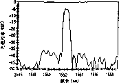
The light amplitude that Fig. 2 has described Waveguide array inside in the array waveguide grating of example 1 distributes.In addition, Fig. 3 describe example 1 array waveguide grating see through spectrum.As can be seen from Figure 3, the array waveguide grating of example 1 forms good basically array waveguide grating, and adjacent crosstalking is approximately-30dB.
(example 2)
The parameter of the array waveguide grating of example 2 is as shown in table 4.The array waveguide grating of example 2 utilizes the said method manufacturing.In example 2, utilize the parameter in the table 4 to make photomask pattern.
Table 4
| Parameter | Design load |
| Number of wavelengths | 16 |
| Channel spacing | 100GHz |
| Free Spectral Range (FSR) | (25.86nm for 32 ripples) |
| The focal length of first and second slab guides | 13580.1μm |
| The optical path difference Δ L of channel waveguide | 63.06μm |
| The order of diffraction | 59 |
| The |
200 |
The light amplitude that Fig. 4 has described Waveguide array inside in the array waveguide grating of example 2 distributes.In addition, Fig. 5 describe example 2 array waveguide grating see through spectrum.As can be seen from Figure 5, the array waveguide grating of example 2 forms good basically array waveguide grating, and adjacent crosstalking is approximately-31dB.
The present invention is not limited to above-mentioned each embodiment, but can adopt different embodiment.For example, the number of channel waveguide is set at 111 in example 1, and the number of channel waveguide is set at 200 in example 2.Yet the number of channel waveguide can be set arbitrarily according to the number of wavelengths of array waveguide grating or the quantity of transmittance wave band.
And each parameter is not limited to parameter shown in example 1 and the example 2 in the array waveguide grating, but can set arbitrarily.Under grating type and flat type both of these case, suitably determine the number of channel waveguide (4a), can improve and crosstalk.
In the above-described embodiments, though array waveguide grating is used as demodulation multiplexer, array waveguide grating is also as multiplexer.In this case, light is from 6 inputs of second optical waveguide, and multiplexed optical is exported from one of first optical waveguide 2.
Claims (16)
1, a kind of array waveguide grating comprises
At least one first optical waveguide;
First slab guide;
Waveguide array, the output terminal of this first optical waveguide are connected to this first slab guide, and the output terminal of this first sheet is connected to this Waveguide array, and described Waveguide array comprises a plurality of channel waveguides, and the length of each channel waveguide differs from one another;
Second slab guide; With
A plurality of second optical waveguides, the output terminal of this Waveguide array are connected to this second slab guide, and the output terminal of this second slab guide is connected to this second optical waveguide,
Wherein the number of a plurality of channel waveguides is defined as making crosstalking and is predetermined value to the maximum, makes light amplitude on the interphase between one of described first optical waveguide and first slab guide distribute and reappears on the interphase between second slab guide and described second optical waveguide basically.
2, array waveguide grating according to claim 1, wherein said predetermined value is approximately-26dB.
3, array waveguide grating according to claim 1, wherein, the light transmission rate of array waveguide grating is Gaussian distribution with wavelength, and wherein the number of a plurality of channel waveguides is defined as making first secondary lobe that the light amplitude that sees through in the Waveguide array distributes and includes only main lobe and appear at the main lobe both sides.
4, array waveguide grating according to claim 3, wherein the number of a plurality of channel waveguides is defined as making light amplitude to distribute and includes only the part of the main lobe and first secondary lobe.
5, array waveguide grating according to claim 3, wherein the number of a plurality of channel waveguides is defined as making light amplitude to distribute and includes only the whole of the main lobe and first secondary lobe.
6, array waveguide grating according to claim 1, wherein, the light transmission rate of array waveguide grating is with the rectangular distribution of wavelength, and wherein the number of a plurality of channel waveguides is defined as making the light amplitude that sees through in the Waveguide array to distribute including only main lobe, appears at first secondary lobe on main lobe both sides and appears at two second secondary lobes in each first secondary lobe outside.
7, array waveguide grating according to claim 6, wherein the number of a plurality of channel waveguides is defined as making light amplitude to distribute and includes only the part of main lobe, first secondary lobe and second secondary lobe.
8, array waveguide grating according to claim 6, wherein the number of a plurality of channel waveguides is defined as making light amplitude to distribute and includes only the whole of main lobe, first secondary lobe and second secondary lobe.
9, a kind of method of manufacturing array waveguide optical grating comprises:
At least one first optical waveguide is provided;
First slab guide is provided;
Waveguide array is provided, and the output terminal of this first optical waveguide is connected to this first slab guide, and the output terminal of this first sheet is connected to this Waveguide array, and described Waveguide array comprises a plurality of channel waveguides, and the length of each channel waveguide differs from one another;
Second slab guide is provided; With
A plurality of second optical waveguides are provided, and the output terminal of this Waveguide array is connected to this second slab guide, and the output terminal of this second slab guide is connected to this second optical waveguide; And
The number of determining a plurality of channel waveguides makes to crosstalk and is predetermined value to the maximum, makes light amplitude on the interphase between one of described first optical waveguide and first slab guide distribute and reappears on the interphase between second slab guide and described second optical waveguide basically.
10, method according to claim 9, wherein said predetermined value is approximately-26dB.
11, method according to claim 9 wherein also comprises:
Array waveguide grating is provided, and light transmission rate is Gaussian distribution with wavelength; With
Determine the number of a plurality of channel waveguides, make first secondary lobe that the light amplitude that sees through in the Waveguide array distributes and includes only main lobe and appear at the main lobe both sides.
12, method according to claim 11, wherein the number of definite a plurality of channel waveguides makes light amplitude distribute and includes only the part of the main lobe and first secondary lobe.
13, method according to claim 11, wherein the number of definite a plurality of channel waveguides makes light amplitude distribute and includes only the whole of the main lobe and first secondary lobe.
14, method according to claim 9 wherein also comprises:
Array waveguide grating is provided, and light transmission rate is with the rectangular distribution of wavelength; With
Determine the number of a plurality of channel waveguides, make the light amplitude that sees through in the Waveguide array distribute and include only main lobe, appear at first secondary lobe on main lobe both sides and appear at two second secondary lobes in each first secondary lobe outside.
15, method according to claim 14 determines that wherein the number of a plurality of channel waveguides makes the light amplitude distribution include only the part of main lobe, first secondary lobe and second secondary lobe.
16, method according to claim 14 determines that wherein the number of a plurality of channel waveguides makes the light amplitude distribution include only the whole of main lobe, first secondary lobe and second secondary lobe.
Applications Claiming Priority (4)
| Application Number | Priority Date | Filing Date | Title |
|---|---|---|---|
| JP2001007867 | 2001-01-16 | ||
| JP2001007867 | 2001-01-16 | ||
| JP2001142859A JP3700930B2 (en) | 2001-01-16 | 2001-05-14 | Arrayed waveguide grating |
| JP2001142859 | 2001-05-14 |
Publications (2)
| Publication Number | Publication Date |
|---|---|
| CN1366193A CN1366193A (en) | 2002-08-28 |
| CN1221825C true CN1221825C (en) | 2005-10-05 |
Family
ID=26607774
Family Applications (1)
| Application Number | Title | Priority Date | Filing Date |
|---|---|---|---|
| CNB021016860A Expired - Fee Related CN1221825C (en) | 2001-01-16 | 2002-01-15 | Array wave guide grating and its making method |
Country Status (5)
| Country | Link |
|---|---|
| US (1) | US6768840B2 (en) |
| EP (1) | EP1223444A3 (en) |
| JP (1) | JP3700930B2 (en) |
| KR (1) | KR100452686B1 (en) |
| CN (1) | CN1221825C (en) |
Families Citing this family (8)
| Publication number | Priority date | Publication date | Assignee | Title |
|---|---|---|---|---|
| JP2007065562A (en) * | 2005-09-02 | 2007-03-15 | Furukawa Electric Co Ltd:The | Array waveguide diffraction grating |
| JP4748524B2 (en) * | 2006-08-31 | 2011-08-17 | 古河電気工業株式会社 | Arrayed waveguide grating type multiplexer / demultiplexer |
| JP5100175B2 (en) * | 2007-03-28 | 2012-12-19 | 古河電気工業株式会社 | Arrayed waveguide grating type multiplexer / demultiplexer |
| JP2010276639A (en) * | 2009-05-26 | 2010-12-09 | Furukawa Electric Co Ltd:The | Arrayed waveguide grating |
| US20110085761A1 (en) * | 2009-05-26 | 2011-04-14 | Furukawa Electric Co., Ltd. | Arrayed waveguide grating and method of manufacturing arrayed waveguide grating |
| JP5432047B2 (en) * | 2010-04-15 | 2014-03-05 | 日本電信電話株式会社 | Optical switch and wavelength selective switch |
| WO2015070389A1 (en) * | 2013-11-13 | 2015-05-21 | 华为技术有限公司 | Waveguide structures, waveguide coupling structures, and manufacturing methods |
| CN107148561B (en) * | 2014-09-10 | 2019-01-11 | 电子光子集成电路股份有限公司 | Curve grating spectrograph and wavelength multiplexer or demultiplexer with high wavelength resolution |
Family Cites Families (5)
| Publication number | Priority date | Publication date | Assignee | Title |
|---|---|---|---|---|
| JP3201560B2 (en) | 1994-06-13 | 2001-08-20 | 日本電信電話株式会社 | Optical signal processing circuit |
| FR2743234B1 (en) | 1995-12-28 | 1998-01-23 | Alcatel Optronics | WAVELENGTH DEMULTIPLEXER |
| JP2858656B2 (en) * | 1997-02-14 | 1999-02-17 | 日立電線株式会社 | Optical wavelength multiplexer / demultiplexer |
| CA2253972C (en) * | 1998-05-29 | 2001-07-31 | Hitachi Cable, Ltd. | Optical wavelength multiplexer/demultiplexer |
| US6298186B1 (en) * | 2000-07-07 | 2001-10-02 | Metrophotonics Inc. | Planar waveguide grating device and method having a passband with a flat-top and sharp-transitions |
-
2001
- 2001-05-14 JP JP2001142859A patent/JP3700930B2/en not_active Expired - Fee Related
- 2001-12-18 US US10/020,220 patent/US6768840B2/en not_active Expired - Fee Related
-
2002
- 2002-01-08 EP EP02250100A patent/EP1223444A3/en not_active Withdrawn
- 2002-01-15 CN CNB021016860A patent/CN1221825C/en not_active Expired - Fee Related
- 2002-01-16 KR KR10-2002-0002415A patent/KR100452686B1/en not_active IP Right Cessation
Also Published As
| Publication number | Publication date |
|---|---|
| KR100452686B1 (en) | 2004-10-14 |
| US20020136492A1 (en) | 2002-09-26 |
| JP3700930B2 (en) | 2005-09-28 |
| JP2002286951A (en) | 2002-10-03 |
| EP1223444A2 (en) | 2002-07-17 |
| EP1223444A3 (en) | 2004-08-11 |
| KR20020061177A (en) | 2002-07-23 |
| CN1366193A (en) | 2002-08-28 |
| US6768840B2 (en) | 2004-07-27 |
Similar Documents
| Publication | Publication Date | Title |
|---|---|---|
| CN1387628A (en) | Phaser with flattened pass-band | |
| JPH116928A (en) | Arrayed waveguide grating type wavelength multiplexer /demultiplexer | |
| CN1221825C (en) | Array wave guide grating and its making method | |
| CN104570200B (en) | Utilize the improved silica base Arrayed Waveguide Grating device of silica-based waveguides and preparation | |
| JP2012014027A (en) | Star coupler and optical multiplexing/demultiplexing device | |
| KR102414506B1 (en) | Echelle lattice multiplexer or demultiplexer | |
| US6529649B1 (en) | Optical filter with improved crosstalk rejection | |
| CN1372156A (en) | Array waveguide raster multiplexer/demultiplexer | |
| US6229938B1 (en) | WDM filter | |
| CN111830628B (en) | Coarse wavelength division multiplexer/demultiplexer and optical communication equipment | |
| WO2012002368A1 (en) | Arrayed waveguide grating optical division multiplexing module | |
| US20030002786A1 (en) | Optical multiplexer/demultiplexer | |
| US6728435B2 (en) | Arrayed waveguide grating type optical multiplexer/demultiplexer and optical waveguide circuit | |
| JP3472247B2 (en) | Waveguide type optical multiplexer / demultiplexer | |
| EP2579076B1 (en) | Optical waveguide and arrayed waveguide grating | |
| JP2000131540A (en) | Optical multiplexing/demultiplexing device | |
| JP4643924B2 (en) | Lattice modulation type photonic crystal wavelength filter, array type wavelength multiplexer / demultiplexer using the same, and manufacturing method thereof | |
| KR20170069900A (en) | Wavelength division device, wavelength division multiplexing system and wavelength multiplexing system | |
| CN106443880B (en) | Demultiplexer with blazed waveguide side wall grating and sub-wavelength grating structures | |
| CN1308432A (en) | Multiplex/demultiplex light path | |
| JP6660985B2 (en) | Wavelength filter | |
| CN1411197A (en) | Plane oprical waveguide segmented Bragg optical grating interleaving apparatus/de-interleaving apparatus | |
| US20040022485A1 (en) | Apparatus and method for producing a flat-topped filter response for (de)multiplexer having a diffraction grating with variable line spacing | |
| US20100110546A1 (en) | Photonics device | |
| JP3691782B2 (en) | Planar optical waveguide circuit manufacturing method |
Legal Events
| Date | Code | Title | Description |
|---|---|---|---|
| C10 | Entry into substantive examination | ||
| SE01 | Entry into force of request for substantive examination | ||
| C06 | Publication | ||
| PB01 | Publication | ||
| C14 | Grant of patent or utility model | ||
| GR01 | Patent grant | ||
| CF01 | Termination of patent right due to non-payment of annual fee |
Granted publication date: 20051005 Termination date: 20160115 |
|
| EXPY | Termination of patent right or utility model |