CN1202545C - Planar electron emitter (PEE) - Google Patents
Planar electron emitter (PEE) Download PDFInfo
- Publication number
- CN1202545C CN1202545C CNB998072478A CN99807247A CN1202545C CN 1202545 C CN1202545 C CN 1202545C CN B998072478 A CNB998072478 A CN B998072478A CN 99807247 A CN99807247 A CN 99807247A CN 1202545 C CN1202545 C CN 1202545C
- Authority
- CN
- China
- Prior art keywords
- electronics
- material layer
- conduction
- layer
- electric charge
- Prior art date
- Legal status (The legal status is an assumption and is not a legal conclusion. Google has not performed a legal analysis and makes no representation as to the accuracy of the status listed.)
- Expired - Fee Related
Links
- 239000000463 material Substances 0.000 claims abstract description 245
- 239000004065 semiconductor Substances 0.000 claims abstract description 184
- 230000005684 electric field Effects 0.000 claims abstract description 56
- 239000013078 crystal Substances 0.000 claims abstract description 19
- 238000000034 method Methods 0.000 claims description 92
- 229910052751 metal Inorganic materials 0.000 claims description 46
- 239000002184 metal Substances 0.000 claims description 44
- XUIMIQQOPSSXEZ-UHFFFAOYSA-N Silicon Chemical compound [Si] XUIMIQQOPSSXEZ-UHFFFAOYSA-N 0.000 claims description 24
- 229910052710 silicon Inorganic materials 0.000 claims description 24
- 239000010703 silicon Substances 0.000 claims description 24
- 239000000203 mixture Substances 0.000 claims description 21
- 239000012535 impurity Substances 0.000 claims description 17
- 238000004519 manufacturing process Methods 0.000 claims description 16
- BASFCYQUMIYNBI-UHFFFAOYSA-N platinum Chemical compound [Pt] BASFCYQUMIYNBI-UHFFFAOYSA-N 0.000 claims description 16
- 238000002360 preparation method Methods 0.000 claims description 16
- 230000005540 biological transmission Effects 0.000 claims description 15
- 229910052782 aluminium Inorganic materials 0.000 claims description 12
- 239000004411 aluminium Substances 0.000 claims description 12
- XAGFODPZIPBFFR-UHFFFAOYSA-N aluminium Chemical compound [Al] XAGFODPZIPBFFR-UHFFFAOYSA-N 0.000 claims description 12
- 239000002019 doping agent Substances 0.000 claims description 11
- 238000001803 electron scattering Methods 0.000 claims description 11
- PCHJSUWPFVWCPO-UHFFFAOYSA-N gold Chemical compound [Au] PCHJSUWPFVWCPO-UHFFFAOYSA-N 0.000 claims description 11
- 229910052737 gold Inorganic materials 0.000 claims description 11
- 239000010931 gold Substances 0.000 claims description 11
- VYZAMTAEIAYCRO-UHFFFAOYSA-N Chromium Chemical compound [Cr] VYZAMTAEIAYCRO-UHFFFAOYSA-N 0.000 claims description 10
- HCHKCACWOHOZIP-UHFFFAOYSA-N Zinc Chemical compound [Zn] HCHKCACWOHOZIP-UHFFFAOYSA-N 0.000 claims description 10
- 229910052804 chromium Inorganic materials 0.000 claims description 10
- 239000011651 chromium Substances 0.000 claims description 10
- 229910052732 germanium Inorganic materials 0.000 claims description 10
- GNPVGFCGXDBREM-UHFFFAOYSA-N germanium atom Chemical compound [Ge] GNPVGFCGXDBREM-UHFFFAOYSA-N 0.000 claims description 10
- 229910052738 indium Inorganic materials 0.000 claims description 10
- APFVFJFRJDLVQX-UHFFFAOYSA-N indium atom Chemical compound [In] APFVFJFRJDLVQX-UHFFFAOYSA-N 0.000 claims description 10
- 239000011159 matrix material Substances 0.000 claims description 10
- 230000003287 optical effect Effects 0.000 claims description 10
- 229910052725 zinc Inorganic materials 0.000 claims description 10
- 239000011701 zinc Substances 0.000 claims description 10
- RYGMFSIKBFXOCR-UHFFFAOYSA-N Copper Chemical compound [Cu] RYGMFSIKBFXOCR-UHFFFAOYSA-N 0.000 claims description 8
- 229910052581 Si3N4 Inorganic materials 0.000 claims description 8
- 229910052802 copper Inorganic materials 0.000 claims description 8
- 239000010949 copper Substances 0.000 claims description 8
- 229910052697 platinum Inorganic materials 0.000 claims description 8
- 229910010271 silicon carbide Inorganic materials 0.000 claims description 8
- HQVNEWCFYHHQES-UHFFFAOYSA-N silicon nitride Chemical compound N12[Si]34N5[Si]62N3[Si]51N64 HQVNEWCFYHHQES-UHFFFAOYSA-N 0.000 claims description 8
- JBRZTFJDHDCESZ-UHFFFAOYSA-N AsGa Chemical compound [As]#[Ga] JBRZTFJDHDCESZ-UHFFFAOYSA-N 0.000 claims description 7
- 229910000673 Indium arsenide Inorganic materials 0.000 claims description 7
- GPXJNWSHGFTCBW-UHFFFAOYSA-N Indium phosphide Chemical compound [In]#P GPXJNWSHGFTCBW-UHFFFAOYSA-N 0.000 claims description 7
- OAICVXFJPJFONN-UHFFFAOYSA-N Phosphorus Chemical compound [P] OAICVXFJPJFONN-UHFFFAOYSA-N 0.000 claims description 7
- MDPILPRLPQYEEN-UHFFFAOYSA-N aluminium arsenide Chemical compound [As]#[Al] MDPILPRLPQYEEN-UHFFFAOYSA-N 0.000 claims description 7
- RPQDHPTXJYYUPQ-UHFFFAOYSA-N indium arsenide Chemical compound [In]#[As] RPQDHPTXJYYUPQ-UHFFFAOYSA-N 0.000 claims description 7
- 229910052698 phosphorus Inorganic materials 0.000 claims description 7
- 239000011574 phosphorus Substances 0.000 claims description 7
- 229910052701 rubidium Inorganic materials 0.000 claims description 7
- IGLNJRXAVVLDKE-UHFFFAOYSA-N rubidium atom Chemical compound [Rb] IGLNJRXAVVLDKE-UHFFFAOYSA-N 0.000 claims description 7
- OKTJSMMVPCPJKN-UHFFFAOYSA-N Carbon Chemical compound [C] OKTJSMMVPCPJKN-UHFFFAOYSA-N 0.000 claims description 6
- 229910052693 Europium Inorganic materials 0.000 claims description 6
- 229910001218 Gallium arsenide Inorganic materials 0.000 claims description 6
- 229910052777 Praseodymium Inorganic materials 0.000 claims description 6
- 229910052772 Samarium Inorganic materials 0.000 claims description 6
- OGPBJKLSAFTDLK-UHFFFAOYSA-N europium atom Chemical compound [Eu] OGPBJKLSAFTDLK-UHFFFAOYSA-N 0.000 claims description 6
- 229910052730 francium Inorganic materials 0.000 claims description 6
- KLMCZVJOEAUDNE-UHFFFAOYSA-N francium atom Chemical compound [Fr] KLMCZVJOEAUDNE-UHFFFAOYSA-N 0.000 claims description 6
- WPYVAWXEWQSOGY-UHFFFAOYSA-N indium antimonide Chemical compound [Sb]#[In] WPYVAWXEWQSOGY-UHFFFAOYSA-N 0.000 claims description 6
- PUDIUYLPXJFUGB-UHFFFAOYSA-N praseodymium atom Chemical compound [Pr] PUDIUYLPXJFUGB-UHFFFAOYSA-N 0.000 claims description 6
- KZUNJOHGWZRPMI-UHFFFAOYSA-N samarium atom Chemical compound [Sm] KZUNJOHGWZRPMI-UHFFFAOYSA-N 0.000 claims description 6
- 229910052712 strontium Inorganic materials 0.000 claims description 6
- CIOAGBVUUVVLOB-UHFFFAOYSA-N strontium atom Chemical compound [Sr] CIOAGBVUUVVLOB-UHFFFAOYSA-N 0.000 claims description 6
- 229910052727 yttrium Inorganic materials 0.000 claims description 6
- VWQVUPCCIRVNHF-UHFFFAOYSA-N yttrium atom Chemical compound [Y] VWQVUPCCIRVNHF-UHFFFAOYSA-N 0.000 claims description 6
- 229910052799 carbon Inorganic materials 0.000 claims description 5
- ZOXJGFHDIHLPTG-UHFFFAOYSA-N Boron Chemical compound [B] ZOXJGFHDIHLPTG-UHFFFAOYSA-N 0.000 claims description 4
- GYHNNYVSQQEPJS-UHFFFAOYSA-N Gallium Chemical compound [Ga] GYHNNYVSQQEPJS-UHFFFAOYSA-N 0.000 claims description 4
- WHXSMMKQMYFTQS-UHFFFAOYSA-N Lithium Chemical compound [Li] WHXSMMKQMYFTQS-UHFFFAOYSA-N 0.000 claims description 4
- 229910052787 antimony Inorganic materials 0.000 claims description 4
- WATWJIUSRGPENY-UHFFFAOYSA-N antimony atom Chemical compound [Sb] WATWJIUSRGPENY-UHFFFAOYSA-N 0.000 claims description 4
- 229910052785 arsenic Inorganic materials 0.000 claims description 4
- RQNWIZPPADIBDY-UHFFFAOYSA-N arsenic atom Chemical compound [As] RQNWIZPPADIBDY-UHFFFAOYSA-N 0.000 claims description 4
- 229910052796 boron Inorganic materials 0.000 claims description 4
- 229910052733 gallium Inorganic materials 0.000 claims description 4
- 229910052744 lithium Inorganic materials 0.000 claims description 4
- 239000007769 metal material Substances 0.000 claims description 4
- 238000004381 surface treatment Methods 0.000 claims description 4
- 229910052715 tantalum Inorganic materials 0.000 claims description 4
- GUVRBAGPIYLISA-UHFFFAOYSA-N tantalum atom Chemical compound [Ta] GUVRBAGPIYLISA-UHFFFAOYSA-N 0.000 claims description 4
- FYYHWMGAXLPEAU-UHFFFAOYSA-N Magnesium Chemical compound [Mg] FYYHWMGAXLPEAU-UHFFFAOYSA-N 0.000 claims description 3
- BUGBHKTXTAQXES-UHFFFAOYSA-N Selenium Chemical compound [Se] BUGBHKTXTAQXES-UHFFFAOYSA-N 0.000 claims description 3
- NINIDFKCEFEMDL-UHFFFAOYSA-N Sulfur Chemical compound [S] NINIDFKCEFEMDL-UHFFFAOYSA-N 0.000 claims description 3
- 239000005864 Sulphur Substances 0.000 claims description 3
- ATJFFYVFTNAWJD-UHFFFAOYSA-N Tin Chemical compound [Sn] ATJFFYVFTNAWJD-UHFFFAOYSA-N 0.000 claims description 3
- 229910052790 beryllium Inorganic materials 0.000 claims description 3
- ATBAMAFKBVZNFJ-UHFFFAOYSA-N beryllium atom Chemical compound [Be] ATBAMAFKBVZNFJ-UHFFFAOYSA-N 0.000 claims description 3
- 229910052797 bismuth Inorganic materials 0.000 claims description 3
- JCXGWMGPZLAOME-UHFFFAOYSA-N bismuth atom Chemical compound [Bi] JCXGWMGPZLAOME-UHFFFAOYSA-N 0.000 claims description 3
- 229910052793 cadmium Inorganic materials 0.000 claims description 3
- BDOSMKKIYDKNTQ-UHFFFAOYSA-N cadmium atom Chemical compound [Cd] BDOSMKKIYDKNTQ-UHFFFAOYSA-N 0.000 claims description 3
- 229910052749 magnesium Inorganic materials 0.000 claims description 3
- 239000011777 magnesium Substances 0.000 claims description 3
- 229910052711 selenium Inorganic materials 0.000 claims description 3
- 239000011669 selenium Substances 0.000 claims description 3
- 229910052714 tellurium Inorganic materials 0.000 claims description 3
- PORWMNRCUJJQNO-UHFFFAOYSA-N tellurium atom Chemical compound [Te] PORWMNRCUJJQNO-UHFFFAOYSA-N 0.000 claims description 3
- 229910052718 tin Inorganic materials 0.000 claims description 3
- 239000003086 colorant Substances 0.000 claims description 2
- 230000003746 surface roughness Effects 0.000 claims description 2
- 229910052792 caesium Inorganic materials 0.000 claims 4
- TVFDJXOCXUVLDH-UHFFFAOYSA-N caesium atom Chemical compound [Cs] TVFDJXOCXUVLDH-UHFFFAOYSA-N 0.000 claims 4
- 239000002772 conduction electron Substances 0.000 claims 1
- 239000012212 insulator Substances 0.000 abstract description 15
- 239000010410 layer Substances 0.000 description 77
- 239000000758 substrate Substances 0.000 description 45
- 238000001259 photo etching Methods 0.000 description 23
- 230000008569 process Effects 0.000 description 22
- 235000012431 wafers Nutrition 0.000 description 21
- 230000004888 barrier function Effects 0.000 description 14
- 238000013461 design Methods 0.000 description 12
- 239000010408 film Substances 0.000 description 12
- 239000011810 insulating material Substances 0.000 description 12
- 238000012545 processing Methods 0.000 description 12
- 238000006243 chemical reaction Methods 0.000 description 11
- 230000000694 effects Effects 0.000 description 11
- 238000005516 engineering process Methods 0.000 description 11
- 238000010586 diagram Methods 0.000 description 10
- 230000033001 locomotion Effects 0.000 description 9
- 230000005669 field effect Effects 0.000 description 8
- 238000005381 potential energy Methods 0.000 description 8
- 238000010521 absorption reaction Methods 0.000 description 7
- 230000003321 amplification Effects 0.000 description 7
- 238000003199 nucleic acid amplification method Methods 0.000 description 7
- 238000001704 evaporation Methods 0.000 description 6
- 239000007789 gas Substances 0.000 description 6
- 239000002784 hot electron Substances 0.000 description 6
- 238000002347 injection Methods 0.000 description 6
- 239000007924 injection Substances 0.000 description 6
- 239000000126 substance Substances 0.000 description 6
- 238000010276 construction Methods 0.000 description 5
- 229910003460 diamond Inorganic materials 0.000 description 5
- 239000010432 diamond Substances 0.000 description 5
- 230000006870 function Effects 0.000 description 5
- 238000010438 heat treatment Methods 0.000 description 5
- 239000002245 particle Substances 0.000 description 5
- 230000015572 biosynthetic process Effects 0.000 description 4
- 230000008859 change Effects 0.000 description 4
- 239000002800 charge carrier Substances 0.000 description 4
- 230000002950 deficient Effects 0.000 description 4
- 239000000428 dust Substances 0.000 description 4
- 230000005670 electromagnetic radiation Effects 0.000 description 4
- 238000010894 electron beam technology Methods 0.000 description 4
- 230000008020 evaporation Effects 0.000 description 4
- 238000009413 insulation Methods 0.000 description 4
- 238000001459 lithography Methods 0.000 description 4
- 238000005036 potential barrier Methods 0.000 description 4
- 230000005855 radiation Effects 0.000 description 4
- 238000003860 storage Methods 0.000 description 4
- 230000015556 catabolic process Effects 0.000 description 3
- 238000001514 detection method Methods 0.000 description 3
- 238000002474 experimental method Methods 0.000 description 3
- 239000011521 glass Substances 0.000 description 3
- 238000005286 illumination Methods 0.000 description 3
- 238000001393 microlithography Methods 0.000 description 3
- 238000005457 optimization Methods 0.000 description 3
- 238000005498 polishing Methods 0.000 description 3
- 230000004044 response Effects 0.000 description 3
- 229920006395 saturated elastomer Polymers 0.000 description 3
- 239000000243 solution Substances 0.000 description 3
- 238000001228 spectrum Methods 0.000 description 3
- XKRFYHLGVUSROY-UHFFFAOYSA-N Argon Chemical compound [Ar] XKRFYHLGVUSROY-UHFFFAOYSA-N 0.000 description 2
- IJGRMHOSHXDMSA-UHFFFAOYSA-N Atomic nitrogen Chemical compound N#N IJGRMHOSHXDMSA-UHFFFAOYSA-N 0.000 description 2
- 230000006399 behavior Effects 0.000 description 2
- 230000008901 benefit Effects 0.000 description 2
- 230000000052 comparative effect Effects 0.000 description 2
- 239000002131 composite material Substances 0.000 description 2
- 239000002178 crystalline material Substances 0.000 description 2
- 230000007547 defect Effects 0.000 description 2
- 238000000151 deposition Methods 0.000 description 2
- 230000008021 deposition Effects 0.000 description 2
- 230000023077 detection of light stimulus Effects 0.000 description 2
- 230000005672 electromagnetic field Effects 0.000 description 2
- 238000005530 etching Methods 0.000 description 2
- 239000000284 extract Substances 0.000 description 2
- 230000002349 favourable effect Effects 0.000 description 2
- -1 hook Chemical compound 0.000 description 2
- 150000002500 ions Chemical class 0.000 description 2
- 230000009467 reduction Effects 0.000 description 2
- 230000003595 spectral effect Effects 0.000 description 2
- 238000012360 testing method Methods 0.000 description 2
- 230000005641 tunneling Effects 0.000 description 2
- 238000003466 welding Methods 0.000 description 2
- 208000012468 Ewing sarcoma/peripheral primitive neuroectodermal tumor Diseases 0.000 description 1
- 108010076504 Protein Sorting Signals Proteins 0.000 description 1
- 230000001133 acceleration Effects 0.000 description 1
- 230000009471 action Effects 0.000 description 1
- 238000013459 approach Methods 0.000 description 1
- 229910052786 argon Inorganic materials 0.000 description 1
- RBFDCQDDCJFGIK-UHFFFAOYSA-N arsenic germanium Chemical compound [Ge].[As] RBFDCQDDCJFGIK-UHFFFAOYSA-N 0.000 description 1
- 238000005452 bending Methods 0.000 description 1
- 230000009286 beneficial effect Effects 0.000 description 1
- 239000010406 cathode material Substances 0.000 description 1
- 230000002860 competitive effect Effects 0.000 description 1
- 238000002109 crystal growth method Methods 0.000 description 1
- 238000009792 diffusion process Methods 0.000 description 1
- 238000009826 distribution Methods 0.000 description 1
- 238000001914 filtration Methods 0.000 description 1
- 229910002804 graphite Inorganic materials 0.000 description 1
- 239000010439 graphite Substances 0.000 description 1
- 238000009434 installation Methods 0.000 description 1
- 230000010354 integration Effects 0.000 description 1
- 230000003993 interaction Effects 0.000 description 1
- 238000010884 ion-beam technique Methods 0.000 description 1
- 230000002427 irreversible effect Effects 0.000 description 1
- 230000007246 mechanism Effects 0.000 description 1
- XZWYZXLIPXDOLR-UHFFFAOYSA-N metformin Chemical group CN(C)C(=N)NC(N)=N XZWYZXLIPXDOLR-UHFFFAOYSA-N 0.000 description 1
- 230000005012 migration Effects 0.000 description 1
- 238000013508 migration Methods 0.000 description 1
- 238000002156 mixing Methods 0.000 description 1
- 230000004048 modification Effects 0.000 description 1
- 238000012986 modification Methods 0.000 description 1
- 229910021421 monocrystalline silicon Inorganic materials 0.000 description 1
- 238000000465 moulding Methods 0.000 description 1
- 230000007935 neutral effect Effects 0.000 description 1
- 229910052757 nitrogen Inorganic materials 0.000 description 1
- 230000008520 organization Effects 0.000 description 1
- 230000003647 oxidation Effects 0.000 description 1
- 238000007254 oxidation reaction Methods 0.000 description 1
- 230000001590 oxidative effect Effects 0.000 description 1
- 229920002120 photoresistant polymer Polymers 0.000 description 1
- 230000000704 physical effect Effects 0.000 description 1
- 238000005293 physical law Methods 0.000 description 1
- 238000003908 quality control method Methods 0.000 description 1
- 230000027756 respiratory electron transport chain Effects 0.000 description 1
- 230000002441 reversible effect Effects 0.000 description 1
- 238000012552 review Methods 0.000 description 1
- 238000004626 scanning electron microscopy Methods 0.000 description 1
- 230000008054 signal transmission Effects 0.000 description 1
- 239000002356 single layer Substances 0.000 description 1
- 239000007787 solid Substances 0.000 description 1
- 239000010421 standard material Substances 0.000 description 1
- 239000010409 thin film Substances 0.000 description 1
- XOLBLPGZBRYERU-UHFFFAOYSA-N tin dioxide Chemical compound O=[Sn]=O XOLBLPGZBRYERU-UHFFFAOYSA-N 0.000 description 1
- 229910001887 tin oxide Inorganic materials 0.000 description 1
- 230000007306 turnover Effects 0.000 description 1
- 230000000007 visual effect Effects 0.000 description 1
Images


Classifications
-
- H—ELECTRICITY
- H01—ELECTRIC ELEMENTS
- H01J—ELECTRIC DISCHARGE TUBES OR DISCHARGE LAMPS
- H01J1/00—Details of electrodes, of magnetic control means, of screens, or of the mounting or spacing thereof, common to two or more basic types of discharge tubes or lamps
- H01J1/02—Main electrodes
- H01J1/30—Cold cathodes, e.g. field-emissive cathode
-
- B—PERFORMING OPERATIONS; TRANSPORTING
- B82—NANOTECHNOLOGY
- B82Y—SPECIFIC USES OR APPLICATIONS OF NANOSTRUCTURES; MEASUREMENT OR ANALYSIS OF NANOSTRUCTURES; MANUFACTURE OR TREATMENT OF NANOSTRUCTURES
- B82Y10/00—Nanotechnology for information processing, storage or transmission, e.g. quantum computing or single electron logic
-
- H—ELECTRICITY
- H01—ELECTRIC ELEMENTS
- H01J—ELECTRIC DISCHARGE TUBES OR DISCHARGE LAMPS
- H01J1/00—Details of electrodes, of magnetic control means, of screens, or of the mounting or spacing thereof, common to two or more basic types of discharge tubes or lamps
- H01J1/02—Main electrodes
- H01J1/30—Cold cathodes, e.g. field-emissive cathode
- H01J1/312—Cold cathodes, e.g. field-emissive cathode having an electric field perpendicular to the surface, e.g. tunnel-effect cathodes of metal-insulator-metal [MIM] type
-
- H—ELECTRICITY
- H01—ELECTRIC ELEMENTS
- H01J—ELECTRIC DISCHARGE TUBES OR DISCHARGE LAMPS
- H01J35/00—X-ray tubes
- H01J35/02—Details
- H01J35/04—Electrodes ; Mutual position thereof; Constructional adaptations therefor
- H01J35/06—Cathodes
- H01J35/065—Field emission, photo emission or secondary emission cathodes
-
- H—ELECTRICITY
- H01—ELECTRIC ELEMENTS
- H01J—ELECTRIC DISCHARGE TUBES OR DISCHARGE LAMPS
- H01J2235/00—X-ray tubes
- H01J2235/06—Cathode assembly
- H01J2235/062—Cold cathodes
Landscapes
- Engineering & Computer Science (AREA)
- Chemical & Material Sciences (AREA)
- Nanotechnology (AREA)
- Theoretical Computer Science (AREA)
- Physics & Mathematics (AREA)
- Crystallography & Structural Chemistry (AREA)
- Mathematical Physics (AREA)
- Cold Cathode And The Manufacture (AREA)
- Cathode-Ray Tubes And Fluorescent Screens For Display (AREA)
- Electron Sources, Ion Sources (AREA)
- Electrodes For Cathode-Ray Tubes (AREA)
- Discharge Lamps And Accessories Thereof (AREA)
- Bipolar Transistors (AREA)
- Crystals, And After-Treatments Of Crystals (AREA)
- Electrodes Of Semiconductors (AREA)
Abstract
A planar electron emitter, based on the existence of quasi-ballistic transport of electrons is disclosed. In its preferred embodiment the planar electron emitter structure consists of a body of finite gap pure semiconductor or insulator, the said body of macroscopic thickness (similar 1mm) being terminated by two parallel surfaces and of a set of two electrodes deposited/grown on the said two free surfaces such that when a low external electrical field (similar 100V/cm) is applied to this structure, consisting of two electrodes and the said semiconductor or insulating body sandwiched between them, a large fraction of electrons injected into the said semiconductor or insulator body from the negatively charged electrode (cathode) is quasi-ballistic in nature, that is this fraction of injected electrons is accelerated within the said semiconductor or insulator body without suffering any appreciable inelastic energy losses, thereby achieving sufficient energy and appropriate momentum at the positively charged electrode (anode) to be able to traverse through the said anode and to escape from the said structure into empty space (vacuum), said semiconductor or insulator body comprises a material or material system having a predetermined crystal orientation.
Description
Technical field
The present invention relates to a kind of new method that produces and conduct accurate ballistic electron when using at the bottom of semiconductor or the insulator-base in being exposed to low electric field.This method will make may be in described semiconductor or insulator accelerated electron and can not suffer any tangible non-resilient energy loss.Its main embodiment will be the plane electronics reflector in flat-panel monitor and the photoetching of plane electronics bundle for example.
Background technology
In various applications, use many devices of described (disclosed) plane electronics reflector also to be disclosed, also apply for priority simultaneously described device.
The accurate ballistic transport of electronics when the present invention relates in high ohmic semiconductor or insulator in being exposed to low electric field (about 100V/cm).The meaning of accurate ballistic transport is that electron scattering reduces to minimum so that as seen electron mean free path becomes naked eyes.This effect so far just when putting on very in the short-range when very high electric field and semiconductor in semiconductor, just detect when being cooled to very low temperature.Be as the criterion ballistic semiconductor or claim QB-Sem of a kind of semiconductor with above-mentioned characteristic or insulating material will be called in the back.
The utilization of accurate ballistic transport can be passed through number of ways.These will be divided into two main fields in this application:
1. electric transmission semiconductor: its characteristic performance transmission performance of ballistic electron in material that be as the criterion in this field, with
2. electron source, the performance of its characteristic performance in this field for launching accurate ballistic electron from substrate.
Relevant prior art had not been mentioned the ballistic electron in high resistivity semiconductor or the insulator, yet not mentioned ballistic electron in being exposed to high electric field the time.This fact is the result who causes owing to the common opinion to accurate ballistic transport in the semiconductor.The possibility of the accurate ballistic transport of highly resistant material is counterintuitive, thereby does not explore as yet so far.Understanding to the basic physical property of this type of ballistic transport is, as long as the electric field E that applies is in ohm scope (density of flexible lamp charge carrier and charge mobility are constant and irrelevant with electric field E), and the thickness of described semiconductor or insulating material (is about 1000-2000 dust (10 to the maximum greater than the mean free path of flexible lamp charge carrier
-10M) in the time of the order of magnitude), at this moment the current component from ballistic electron is little of insignificant, and causing electron emission current is null value substantially.(as a reference, referring to S.M.Sze: semiconductor device physics; John wiley 1981 or K.W.Boer: Semiconductor Physics summary, II volume; VanNotrand Reinhold 1992).
1. electric transmission semiconductor
Electronics is the accurate ballistic transport when being exposed in the low electric field (about 100V/cm) in high resistivity semiconductor or insulator, is a kind of performance that can be used for any semiconductor element or device to some extent.
Semiconductor element and device comprise wide application and claim, and the reference in this scope is a large amount of.It makes 4 kinds of application types, and each class has the example of product.
Category-A: rectification and electric charge (information) are stored
This based semiconductor device/device comprises Schottky barrier diode (US5627479 and EP672257B1), bipolar p-n, p-i-n diode, transistor and many unipolar devices, MIS (metal-insulator semiconductor) diode for example, CCD (charge coupled device), the MIS tunnel diode, the MIS switching diode, IMPATT (impact avalanche and transit time) diode and BARITT (potential barrier injection and transit time) diode and other relevant transit time device.
Category-B: photosensitive and luminescent device
This based semiconductor device/device is comprising LEDs (light-emitting diode), and photodiode, semiconductor laser, avalanche diode and other are used for the photoconductive device of photosignal conversion purpose.
C class: amplify and fixed storage
The present invention comprises bipolar transistor and bipolar unijunction transistor in the application aspect this based semiconductor device/device, together with many unipolar components and device, comprise FETs (field-effect transistor), JFETs (junction field effect transistor), MESFETs (metal-semiconductor field effect transistor), MOSFETs (MOS (metal-oxide-semiconductor) memory) and permanent memory.Relevant especially with the present invention in this type of is tunnel transistor, TEDs (transmission electronic device) and other trajectory (hot electron) transistor AND gate/or device.
D class: the detection of light image, formation and processing
Semiconductor gamma camera, the signal of telecommunication are to the conversion of two-dimentional light image/signal, and two light images/luminance signals/contrast is amplified with the space and amplified.
Ballistic electron device or be called the existing in the past people of hot-electron device and proposed (as an example referring to S.M.Sze: semiconductor device physics; The 184th page of John Wiley 1981, and K.W.Boer: Semiconductor Physics summary, II volume; Wan Nostrond Reinhold 1992 the 1265th and 1247 pages), but the structure producing cost that proposes is high and unreliable, requires minimum size (the 100 dust order of magnitude) and high electric field.
2. electron source
The present invention relates to the general type of a kind of being called " electron source ", more specifically to the electronic device of " plane electronics source " subclass of a kind of being called.All these devices provide a branch of and can move through the region of no pressure and can be used for the electronics that various technology are used.
The basic demand of all electron sources is electronics that the emitting surface (towards the device surface of vacuum) at device provides capacity, and enough energy (in most cases for 3-5eV) and the speed of an edge towards the emitting surface direction are arranged, so that make these electronic energies pass the energy barrier of emitting surface-vacuum interface and escape into vacuum from material.Energy barrier is provided by the difference between the electron chemistry potential energy at vacuum level and emitting surface place roughly.The energy that needs can be by arbitrary the providing in the following method:
Heating emitting surface (" heat emission " electron source).
In emitting surface-vacuum area, set up a sufficiently high electric field (" emission " electron source).
Along the electronics in the essential part zone of the device that fully quickens towards the direction of emitting surface (" emission of field, tunnel " and " emission of field, tunnel " electron source).
By photon or other high energy particle irradiation emitting surface (" light emission " electron source).
Reduce the described energy barrier (" negative electron affinity emission " electron source) at emitting surface-vacuum interface place.
Or any combination by said method.
Although some purposes is required a point-like electron electron gun, electronics is accelerated continuously and carries out electronics-light modulation under this occasion, has a large amount of technology to use, and requires a plane electronics source and this electron source comparatively favourable under this occasion.When this moment, all prior aries were used for these application, all relate to point shape emitter region from a special material part.A bigger plane electronics reflector can only obtain by the array of making a this sub-district.In addition, most of device needs the opening in the anode to be used to allow electronics escape into vacuum.
Very a large amount of inventions is arranged, as can from the quoted passage of for example US5703435 (in December, 1997) and US5534859 (in September, 1996), seeing, all mainly focus on these inventions of use as the basic structural unit in the Field Emission Display all about the plane electronics reflector.
Most of prior art can generally be divided into two types.
The first kind
In the first kind, the K-A emitting structural all is solid-state structure usually and is constituted by metal, semiconductor and insulating material, so that be based upon the necessary condition that cathode surface-vacuum space produces electronic field emission at the interface.The purpose of these devices is to improve electronic transmitting efficiency, all use same substrate above have the negative electrode of some deposited material.Electronics is injected free space from semiconductor surface by the aperture the anode.Its principle is the potential barrier of doing narrow semiconductor free space potential barrier and enabling to escape and pass anode for momentum electronics.Any said method can be used to increase electron emission current I
Em
In a special characteristic of the first kind most of solid state device of the prior art, be to apply high external voltage in the short-range (having the electron mean free path order of magnitude) very much, so that making, the enough strong electric field of generation is convenient to produce and accelerated electron.These electronics are advanced to the emission anode surface along the track that can be described as accurate trajectory (common here avalanche multiplication that also stands electronics) in described electric field then.Yet simultaneously, they are expert at and emit considerable energy by inelastic collision (scattering) on the route.Present understanding is to apply high voltage for obtain significant electron emission requirements by the method.If apply low electric field E (in ohm scope, the density of flexible lamp charge carrier and charge mobility are constant and irrelevant with electric field E), and the thickness L of semiconductor or insulating material
Sem(Fig. 2) greater than the average free radius (being the 1000-2000 dust order of magnitude to the maximum) of flexible lamp charge carrier, current component I at this moment
BalLittle of insignificant, cause electron emission current I
EmBasic is null value (Fig. 2).
Some selected first kind prior art is described in detail in detail below, and other relates in the end of this section.
US5536193 relates to a kind of method of making field emission device and uses the following step: diffusion wide bandgap materials in a small amount on substrate, covered with metal, and etching metal appears until wide bandgap materials, makes several and is used for the small peak of emitting electrons.
US5463275 only illustrates that electron emission device comprises a layer structure that is made of at least 3 kinds of special selected semi-conducting materials.
US4801994 relates to 3 layers of semiconductor structure, and wherein the intermediate layer is assumed to an intrinsic semiconductor, supposes that it should be with very low loss transmission electronic.
GB1223729 (North American Rockwell Corporation) has described a kind of electronics emission tunnel cathode, comprises the sandwich construction that is described in this invention accompanying drawing 2.Electronics is provided by basalis (negative electrode) 21, by insulation barrier 22 transmission, and from emission layer (anode) 23 emissions.By applying a bias voltage, electronics is excited to upper state by insulation barrier 22, as shown in Figure 4 by quantum mechanical tunneling (Fowler-Nordheim tunnel effect).Thin film positive pole layer 23 is suitable for transmitting some electrons excited (Fig. 4,98-118 is capable) at least owing to have very little thickness and the monocrystalline character of reduction ballistic electron-electron collision probability.Offer the electronics of anode layer 23, promptly those have obtained to surpass the electronics (hot electron) of the necessary energy of thermal energy by barrier layer 22 by the quantum mechanical tunneling process, no longer further obtain energy in their motion processes in anode region.The preparation of anode layer 23 provides the transparency that is used for the ballistic electron layer.
EP504603B1 comprises that one of configuration has special impurity level so that influence the complicated semiconductor structure of different depletion regions.This explanation discloses one and has used a Schottky barrier metal semiconductor junction so that improve emission effciency.
US5554859, US4303930 and GB1303659 comprise the scope that is similar to EP504603B1.
Other relevant reference is: metal-insulator-metal type electron field emitter (Physical Review Letters the 76th volume, 17 (1996), 320) electron field emitter (US 5631196, US5703435 and their quoted passage) that, comprises various forms diamond like carbon element in addition.
Second class
Under some situation of described prior art, the feature of the first kind (by more or less planar metal, the semiconductor of all thickness are formed with insulating material) combines with the feature of shape with the form/density that relates to necessary electric field.Usually prepare emitting cathode in this case so that carry out the field emission of electronics from a single-point.This can have the material of low electronic work function and the geometry of moulding material obtains to produce a launch point or spike by cover one on little regional area.
Comment some second selected class prior art below, other relates in the end of this section.
US 5229682 relates to an electronic field emission device, and wherein electronics sends from the part of emission electrode, by the direct freedom of entry of an aperture space in comparative electrode and the intermediate layer.Semiconductor or insulator layer in the middle of electronics does not cross.Emitter is shaped so that have a part of having alarmmed by aperture in opposite electrode and the intermediate layer.A flat-panel monitor is made by the array of a kind electrode.
US 5712490 relates to a kind of photocathode device, comprises some several semiconductor layers that are arranged on the Window layer, and these semiconductor layers are photoconduction the best through selecting to optimize the absorption electronic capability, increase the scattering length of those electronics.This invents a unexposed transparent electrode (being listed as the 11st row referring to the 3rd) that is arranged between the Window layer and first semiconductor layer.
US 5528103 is as US 5229682, but also comprises the focusing ridge, its objective is that producing one causes that electronics injects electric field between them from control electrode, makes electronics be converged to an arrowband, rather than in order to absorb electronics.And, these electrodes/focusing ridge must be the conduction (just like be set out in addition the 7th be listed as the 27th the row in) so that can be in order to reach their purpose.
US 5212426 is as US 5229682, but comprises that also each electrode (pixel) is had an integrated manipulator, and the dress transistor controls is supplied with the electric charge of each emission electrode in using.
US 4823004 relates to a device and is used for the trajectory track of analytical electron by a kind of material, and by analyzing the body inner structure of trajectory track acquisition about material.
US 5444328 relates to a kind of method, is used for a kind of less method construct high voltage electronics emission semiconductor structure that may cause electrical breakdown.
US 5631196 is as US 5229682, but has flat emission electrode, and the part of having alarmmed by aperture in comparative electrode and the intermediate layer is partly replaced as electronic emitting material by doping diamond.
Other relevant reference is: US 4683399, EP150885B1, EP601637A1, US5340997 and their quoted passage.
Exception
The exception of the above-mentioned type comprises these devices, injects vacuum space between the two poles of the earth by apply enough voltage electronics between negative electrode and anode in these devices.In this case, emitting cathode cover by a kind of material with low electronic work function usually and through geometrical figuration so that electronic field emission.An example of this device is:
US5703435 relates to a field-transmitting cathode, and wherein the material of electron emission layer comprises mixture or noncrystal diamond of graphite and diamond crystal.
Use
In order in the device that is fit to, to utilize electric transmission semiconductor and electron source, must do some expansions to the primary element of in the prior art joint, describing.
Electrons emitted may thereby must further be quickened not for the due enough energy of the purpose that reaches them.This typically by be equipped with in certain distance from emitting surface one at " accelerating electrode " under the high normal potential thus in middle vacuum space electrons emitted being accelerated to higher-energy realizes.
For realizing electronics-light conversion purpose, can in anode construction, introduce " luminous element " material that is suitable for, described anode construction becomes an integration section of K-A structure, or is a part of leaving " accelerating electrode " of a definite vacuum range of K-A structure.
The application typical case of electronic source device comprises the electron microscope of form of ownership, the photoetching of plane electronics bundle, the electron gun that evaporating materials is used, X-ray tube, electron multiplier (light multiplier, two-dimentional particle/electromagnetic radiation detector array), electron beam welding machine, flat-panel monitor (based on electronic field emission), and some quick ballistic semiconductor device and devices.
Existing photoetching technique
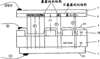
Of the present invention one very important use be in photoetching (micro-lithography) field, more specifically saying so is called in plane electronics bundle photoetching (PEBL) field in the literature.Lithography step is absolutely necessary in integrated circuit (IC) production process.The photoetching part that IC produces be included in substantially by one " writing implement " resist is deposited on wafer and bear on the surface of expose portion of radiation (photon, electronics or ion) and the last repeating step of removing resist in.The photoetching of light, X ray and electron/ion beams is known method, and they can finish the photoetching task of IC production period substantially.The light photoetching is standard, quite ripe industrial technology; Their major defect is that diffraction of light has limited printable minimum details.Usually for to reduce in the further competition of IC element and ICs size, have to think that this is an important shortcoming.By using electronics, the restriction of optical diffraction has not been existed as radiation source.The plane electronics bundle photoetching principle schematic of using in the prior art is illustrated among Fig. 8.The basic structure that its uses comprises negative electrode 1, one deck thin dielectric film 24, an Electron absorption template 19 and anode 4.The electronics quantum just directly passes thin dielectric film 24 and injects free space FS by surperficial S4 in the place of contact with electric matter film at anode.These electronics are accelerated and project on the wafer of the responsive resistant layer 6 of electronics that has pre-deposition then.In people's (comprising some inventor of the present invention) such as the breadboard H.Ahmed of Cambridge Cavendish in 1989 " micro-lithography discussion collection of thesis ", rule of thumb point out and demonstrated how to carry out the photoetching of plane electronics bundle in practice.In the prior art, use a prior art plane electronics reflector example that electron lithography system has been described.Yet, this susceptible electronic emitter has other shortcoming: the plane electronics reflector that is suitable for this purposes can expose whole wafers by a broad beam, but, under essential voltage, because the effect that essential high electric field and short distance cause causes the life-span of these plane electronics reflectors extremely short.
The invention provides a solution to this problem.
A shortcoming of existing field emission planar electronic device is, must apply high external voltage in very short relatively distance range (order of magnitude of electron mean free path), makes and is convenient to emission and accelerated electron so that produce sufficiently high electric field.
Another shortcoming is, in very short relatively distance range, apply this requirement of very high internal field relatively, quality together with the acquisition material, cause following result: shortened electron mean free path (strengthen scattering ratio), then in fact set up to the electronics in the described device can by but do not produce the too significantly restriction of the possible actual range of energy loss.
Also have a shortcoming, because result above-mentioned, these electronics have only sub-fraction to have enough energy enter adjacent cathodes-anode construction to escape anode (emission) surface space.
Have a shortcoming to be again, these devices have quite little electron emission current I usually
Em(Fig. 2) with big background current I
Back(Fig. 2).
Another shortcoming of existing field emission planar electronic device is that they suffer for example excessive weakness of electric power consumption of every square centimeter of electron emission surface area.
It is that The above results causes low electronic transmitting efficiency that a shortcoming is arranged again.
Another shortcoming of existing field emission planar electronic device is, they are usually unstable and be easy to dielectric breakdown, and this seriously limits their life-span usually.
Another shortcoming of described device is and since in the key area of described device (in very short-range high electric field scope) big energy loss that they are suffered is frequent overheated.
Have a shortcoming to be again, the expansion in proportion of these plane electronics feds (increasing the electron emission region of negative electrode) constitutes serious problems.
Another shortcoming of described device is that they use expensive non-standard material.
Another shortcoming of existing field emission planar electronic installation is that structure is too complicated.
Be applicable to that another shortcoming of plane electronics reflector that exposes a broad beam of emission of wafer in the IC manufacture process is, their life-span is extremely lacked (less than 30 minutes), and this makes them not be suitable for the photoetching of plane electronics bundle.
Summary of the invention
The electric transmission semiconductor
The present invention is intended to by using existing, in normal working conditions, and with quite simple semiconductor and insulator structure, by means of accurate ballistic electron, to solve above-mentioned shortcoming.
An object of the present invention is to make and can use a semiconductor or insulator substrates, when described substrate bear low extra electric field (≤100V/cm) time electronics in this substrate along accurate trajectory orbital motion.The side (Fig. 3 surperficial S2) of electronics (accurate ballistic electron) along these tracks from substrate be to opposite side (surperficial S4) motion, and be accelerated to energy and be enough to pass electron emitting surface S4 and escape into vacuum.(described from now on substrate is also referred to as accurate ballistic semiconductor substrate-" QB-Sem substrate ".)
Another object of the present invention is to make to use a kind of QB-Sem substrate, does not change when accurate ballistic electron almost has energy loss and momentum during by this QB-Sem substrate motion.
Another purpose of the present invention is to make to use a kind of QB-Sem substrate, and this substrate does not produce heat when it is used for the accurate ballistic transport of accurate ballistic electron.
Another purpose of the present invention is to make to use a kind of QB-Sem substrate, and accurate ballistic transport can and produce in macroscopic distance range under low (ohm) electric field in this substrate.
Another purpose of the present invention is to make to use a kind of QB-Sem substrate, and velocity of electrons is not subjected to the restriction of high electric field mobility saturation effect in this substrate.
Another purpose of the present invention is to make to use a kind of QB-Sem substrate, and the behavior of electronics is similar to the behavior of electronics in vacuum tube in this substrate.
Another purpose of the present invention is to make to use a kind of QB-Sem substrate, and it does not require high electric field and minimum substrate thickness (the 100 dust order of magnitude).
Another purpose of the present invention is to make to use a kind of QB-Sem substrate, but the semiconductor device simple, sturdy and durable by its production structure, cheap, that reliability is high and the life-span is long.
Another purpose of the present invention is to make to use a kind of QB-Sem substrate, is used in the field of electronics-light application.
Another purpose of the present invention is to make to use a kind of QB-Sem substrate, is used for the design and the manufacturing of semiconductor element and device and integrated circuit (ICs).
Another purpose of the present invention is to make to use a kind of QB-Sem substrate, in this substrate, because the unusual low power loss of QB electronics in the QB semiconductor, thereby the heating problem when helping to solve element when use high-bulk-density in ICs.
Another purpose of the present invention is to make to use a kind of QB-Sem substrate, so that make the design of " hot electron " device needn't depend on complicated film multiple structure, this structure is often unreliable and manufacturing expense is expensive.
Another purpose of the present invention is to make to use a kind of QB-Sem substrate, and it does not need high electric field, so that eliminate various semiconductor device basically by going bad that irreversible dielectric breakdown causes.
Another purpose of the present invention provides the QB-Sem substrate, and they can utilize the conventional semiconductor technology all integrated.
Another purpose of the present invention provides the QB-Sem substrate, and they can utilize existing integrated circuits technology and achievement all integrated.
Another purpose of the present invention provides the QB-Sem substrate, and the design of carrying out quick and high-frequency semiconductor element and device with them will not be subjected to the constraint of geometry.
Another purpose of the present invention provides the QB-Sem substrate, owing to there have been them new design concept about semiconductor element/device and actual device may occur.
Another purpose of the present invention provides the QB-Sem substrate, and they have the life-span with common semi-conductor industry product same order (or longer).
In the QB semiconductor, electronic energy under the low extra electric field in macroscopic distance range valid ballistic movement, by this result disclosed by the invention, will produce significant impact with the various semiconductor elements of one pole type and the design and the structure/manufacturing of device to bipolar.These will be as unit in the integrated circuit structure or components/parts.
Electron source
An object of the present invention is to provide electronic emitter, wherein electrons emitted stands low extra electric field at one and (uses macroscopic accurate trajectory track (these tracks are long as the hundreds of micron) in≤100V/cm) the QB-Sem substrate.Side along those tracks from substrate (Fig. 3 surface S2) is accelerated to opposite side (surperficial S4) ELECTRON OF MOTION (accurate ballistic electron), has increased their energy thus, thereby has escaped into vacuum by electron emitting surface S4.
Another object of the present invention provides the plane electronics reflector, it is characterized in that applying very low electric field/voltage.
Another purpose of the present invention provides the plane electronics reflector, it is characterized in that very low power loss.
Another purpose of the present invention provides thin (≤1cm) the plane electronics reflector that has whole solid-state structures.
Another purpose of the present invention provides the plane electronics reflector, and wherein macroscopic emitting surface is not divided again.
Another purpose of the present invention provides the plane electronics reflector, it is characterized in that assembling simple and sturdy and durable (Fig. 3).
Another purpose of the present invention provides the plane electronics reflector, it is characterized in that being assembled into self supporting structure.
Another purpose of the present invention provides the plane electronics reflector, wherein the restriction that physical dimension of electron emitting surface is not enlarged.
Another purpose of the present invention provides the plane electronics reflector, and wherein the electron emission region area is subjected to the restriction of QB semiconductor wafer lateral dimension greatly and only, and this emission area is about 800cm at present
2(this restriction can be overcome by making module certainly).
A further object of the present invention provides the electronic emitter that is applicable to the photoetching of plane electronics bundle.
The number that the technology of the accurate ballistic electron reflector in plane is used is a lot, and founder of the present invention is intended that same application the present invention application in these areas.These applications comprise method and apparatus/product, for example plane electronics bundle photoetching, Field Emission Display, (low-loss) signal transmitting apparatus at a high speed, high performance detector, high efficiency light source, electron emission microscope, two-dimensional electromagnetic radiation and particle detector array, at a high speed easy integrated semiconductor device, various (novel) electron sources and many other devices.
In first aspect,, provide a kind of electron emission device to comprise according to above-mentioned purpose of the present invention:
-one has first and second surface and comprises a separately element of this first and second surperficial material layer, and wherein first surface is suitable for keeping a kind of first electric charge, and second surface is suitable for keeping a kind of second electric charge,
-being used to provide the device of the electric field that crosses at least a portion element, described device comprises:
-provide the device of first electric charge to the first surface of element, with
-device of second electric charge is provided to the second surface of element, second electric charge is different with first electric charge, so that along be basically perpendicular at least first or the direction of second surface move a plurality of electronics by element, and the part in described at least a plurality of electronics is from this element emission
Wherein:
This material layer of-preparation so that by it being become have perpendicular to first or the monocrystal material of the predetermined crystal orientation of second surface, and is lower than 10 by having
14Cm
-3Impurity concentration, thereby reduce electron scattering in this material layer, wherein this material layer is a semiconductor layer.
In second aspect, the present invention relates to a kind of device, comprising:
-one element with first and second surf zone, wherein
-first surface zone is suitable for keeping a kind of first electric charge, and the second surface zone is suitable for keeping a kind of second electric charge, and wherein
-this element comprises a kind of material or material system, is prepared into the electron scattering that make to reduce in this material or the material system, and have one predetermined perpendicular to first or the crystal orientation of second surface,
-device that crosses the electric field of at least a portion element is provided, described device comprises:
-provide the device of first electric charge to the first surface zone of element, and
-provide the device of second electric charge to the second surface zone of element, second electric charge and first electric charge not jack per line so that the electronics between mobile first surface zone and the second surface zone.
Material or material system according to first aspect and second aspect can comprise a kind of semiconductor, for example silicon, germanium, carborundum, arsenic germanium, indium phosphide, indium arsenide, aluminium arsenide, zinc telluridse or silicon nitride or their any combination.
Be to reduce electron scattering, thereby and be beneficial to the existence of accurate ballistic electron, this material or material system one or more following dopants that can mix: phosphorus, lithium, antimony, arsenic, boron, aluminium, tantalum, gallium, indium, bismuth, silicon, germanium, sulphur, tin, tellurium, selenium, carbon, beryllium, magnesium, zinc or cadmium.Predetermined doped level can be lower than 1 * 10
18Cm
-3, for example be lower than 1 * 10
16Cm
-3, for example be lower than 1 * 10
14Cm
-3, for example be lower than 1 * 10
13Cm
-3, for example be lower than 1 * 10
12Cm
-3
Provide the device of first electric charge can comprise first material or the material system of conduction at least in part to first surface.Equally, provide the device of second electric charge can comprise second material or the material system of conduction at least in part to second surface.
Dao Dian first and second material or material system constitute each and have first and second surperficial thin layer at least in part.These two thin layers can comprise one or more following materials: gold, chromium, platinum, aluminium, copper, hook, rubidium, rubidium, strontium, indium, praseodymium, samarium, yttrium, francium or europium or their any combination.
For providing energy to system, the second surface of first thin layer can effectively be connected with the first terminal of a charge reservoir, and first surface can directly contact with the material of element or the first surface of material system.Equally, the first surface of second thin layer can effectively be connected with second terminal of charge reservoir, and second surface can directly contact with the material of element or the second surface of material system.
Charge reservoir can comprise that a storage battery or any other can provide the energy of direct current or alternating current to device.
First and second thin layer can comprise that a kind of metal or a doped level are higher than 1 * 10
17Cm
-3High doping semiconductor.
The third aspect the present invention relates to a kind of method of launching first kind electronics, and described method comprises step:
-provide one to have first and second surperficial element, wherein
-first surface is suitable for keeping a kind of first electric charge, and second surface is suitable for keeping a kind of second electric charge, and first surface is substantially parallel with second surface,
-preparation material layer, thereby so that by make have perpendicular to first or the predetermined crystal orientation of second surface the track of material layer inner trajectory or the transmission of accurate ballistic electron is provided, and prepare this material layer, so that be lower than 10 by making to have
14Cm
-3Thereby impurity concentration reduce electron scattering in this material layer, wherein this material layer is a semiconductor layer,
-provide first electric charge to the element first surface, and
-providing second electric charge to the element second surface, second electric charge is different with first electric charge, so that in this material or material system, set up an electric field, and
-be basically perpendicular to first or the direction of second surface transmit many electronics by this material layer along trajectory or accurate ballistic trajectory, at least a portion in wherein said many electronics is launched.
Herein, first kind electronics can comprise the electronics that passes element with normal loss, and second electron-like can comprise accurate ballistic electron.
The material or the material system that constitute at least a portion element can comprise semi-conducting material.Relevant with a first aspect of the present invention and second aspect, the table of various suitable material or their combination has been proposed.Equally, preparation work can comprise uses above-mentioned dopant and doped level to mix, so that reduce the scattering of accurate ballistic electron.
For moving accurate ballistic electron, can between first and second surface of element, apply the potential difference that is higher than 2V.And provide the suitable material of first and second electric charge or material system can comprise that a kind of metal or a kind of doped level are higher than 1 * 10 to element
17Cm
-3The high doping semiconductor material.These examples of material are: gold, chromium, platinum, aluminium, copper, hook, rubidium, strontium, indium, praseodymium, samarium, yttrium, francium or europium or their any combination.
In fourth aspect, the present invention relates to a kind of method of making a kind of electron emission device, described method comprises step:
-provide one to have first and second surperficial semiconductor material layer, second surface is substantially parallel with first surface, prepare this material layer, thereby so that by making the predetermined crystal orientation that has perpendicular to first and second surface be provided at trajectory or accurate ballistic electron transmission locus in this material layer, prepare this material layer, so that have one and be lower than 10 by making
14Cm
-3Thereby impurity concentration reduce electron scattering in this material layer,
-provide one to first and second surperficial surface treatment so that reduce surface roughness,
-provide one at least in part the conduction first material or material system, described first material or material system constitute the layer with first and second surface, wherein second surface effectively is connected with the first terminal of a charge reservoir, and wherein first surface directly contacts with the first surface of the material layer of element, and
-provide one at least in part the conduction second material or material system, described second material or material system constitute the layer with first and second surface, wherein first surface effectively is connected with second terminal of charge reservoir, and wherein second surface directly contacts with the second surface of the material layer of element.
About above-mentioned material or material system, relevant with first and second aspect of the present invention, a suitable table for selection material or their combination has been proposed.Equally, preparation work can comprise uses above-mentioned dopant and doped level to mix, so that reduce the scattering of accurate ballistic electron.
Predetermined crystal orientation can comprise<111 〉,<110 or<100, or be applicable to any other crystal orientation of element crystal structure.Surface treatment can comprise different types of technology, for example etching and polishing.Polishing can comprise optics and mechanical polishing.
About dopant, they can be selected from the material group of lithium, phosphorus, antimony, arsenic, boron, aluminium, tantalum, gallium or indium or their any group of Yu.Doped level can be lower than 1 * 10
18Cm
-3, for example be lower than 1 * 10
16Cm
-3, for example be lower than 1 * 10
14Cm
-3, for example be lower than 1 * 10
13Cm
-3, for example be lower than 1 * 10
12Cm
-3
Dao Dian first and second material or material system can comprise that a kind of metal or a kind of doped level are higher than 1 * 10 at least in part
17Cm
-3The high doping semiconductor material.The material that is suitable for can comprise gold, platinum, chromium, aluminium or copper or their any combination.
Aspect the 5th, the present invention relates to a kind of flat-panel monitor and comprise:
-one goods according to first aspect present invention, these goods also comprise:
-one material layer that is suitable in being exposed to electronics time emission multi-wavelength light, described material layer is determined the two-dimensional matrix with one or more surface elements in first and second surperficial plane that is basically parallel to element, each surface element is suitable for launching a kind of light of predetermined wavelength, and
-be used for selectively providing the device of electronics to one or more surface elements of two-dimensional matrix.
The material layer of emission multi-wavelength light can comprise a kind of suitable luminous element or the color TV fluorescent material of standard.This material layer can be by first or second surface support of element.Perhaps, this material layer can be by an add-on parts support.
For obtaining full-color information, the light of emission can comprise at least 3 kinds of wavelength corresponding at least 3 kinds of colors.By these 3 kinds of color combinations, should be able to derive any color in the visual range.The wavelength of emission can be corresponding to red, yellow and blue look, or corresponding to red, green and blue look.
The device of selecting can comprise a pattern in case one be basically parallel to first or the plane of second surface in determine the two-dimensional matrix of an electric controlled member, described pattern is by the material or the material system of conduction constitute at least in part.
Aspect the 6th, the present invention relates to a kind of method that is used for film is exposed to many electronics, described method comprises step:
-electronic emitter according to foregoing invention is provided,
-provide one second element, described second element to be suitable for keeping being exposed to film by in the electronic emitter electrons emitted,
-provide a absorbed layer between first and second element, described suction layer to be suitable for absorbing by the reflector electrons emitted in the position of determining by pattern through composition,
-provide first electric charge to the first surface of the material layer of electronic emitter,
-provide second electric charge to the second surface of the material layer of electronic emitter, the opposite in sign of second electric charge and first electric charge so as from first surface to the second surface mobile electron, and
-film of second element is exposed at least among some electronics that is not absorbed by the absorbed layer through composition by the electronic emitter emission.
About above-mentioned material or material system, relevant with first and second aspect of the present invention, a suitable table for selection material or their combination has been proposed.Equally, preparation work can comprise that above-mentioned dopant and doped level mix so that reduce the scattering of accurate ballistic electron.
First and second terminal by the charge storage device provides first and second electric charge respectively to first and second surface of first element, and wherein the potential difference between first and second terminal of charge reservoir is higher than 2V.The 3rd terminal by charge reservoir provides tricharged to second element.
Second element can comprise a kind of metal or a kind of semi-conducting material, for example silicon, germanium, carborundum, GaAs, indium phosphide, indium antimonide, indium arsenide, aluminium arsenide, zinc telluridse or silicon nitride or their any combination.
At last, first kind electronics can comprise the electronics that passes element with normal loss, and second electron-like can comprise accurate ballistic electron.
Description of drawings
Briefly introduce accompanying drawing below.
Fig. 1 is according to the electron energy band rough schematic view when applied voltage is zero of the present invention.
Fig. 2 is when the electron energy band rough schematic view that adds when determining voltage according to of the present invention.
Fig. 3 is a simplified model according to the basic structure of plane electronics reflector of the present invention.
Fig. 4 is that a flat-panel monitor represents that luminous element is placed between QB Semiconductor substrate and the anode through the diagrammatic side view of the electrode and the luminous element of composition.
Fig. 5 is the top view of Fig. 4.
Fig. 6 is an alternate embodiment according to the flat-panel monitor of Fig. 4, and wherein luminous element is placed on the back of anode.
Fig. 7 is another alternate embodiment according to the flat-panel monitor of Fig. 4, wherein introduce an electronics intensifying ring, and luminous element is placed on the back of intensifying ring.
Fig. 8 is the diagrammatic side view of plane electronics reflector that is used for the prior art of plane electronics bundle photoetching.An Electron absorption material pattern is placed between QB semiconductor and the anode.Additional electronics accelerator card, and the substrate that exposes is placed on the front of this accelerator card.
Fig. 9 is an alternate embodiment according to Fig. 8, and wherein the substrate of Bao Luing is placed on the back of electronics accelerator card and the outside of vacuum, and the entire infrastructure of QB semiconductor and electrode is placed in a vacuum.
Figure 10 is the isoboles of Fig. 8 but has an accurate ballistic electron reflector in the plane according to a most preferred embodiment of the present invention.
Figure 11 is a schematic representation of apparatus of implementing the accurate ballistic electron emission in plane in the photoetching of a plane electronics bundle.
Figure 12 is the photo of Figure 11 device.
Figure 13 is a possible template of mentioning among Figure 10.
Figure 14 is the photo of a scanning electron microscopy, and expression is by some structure of plane electronics bundle photoetching making.
Figure 15 is the 3-D view of an expression according to the embodiment inside of two-dimentional illuminatian plate.
Figure 16 is the 3-D view of expression Figure 15 embodiment outside.
Figure 17 is an alternate embodiment according to two-dimentional illuminatian plate.
Figure 18 be one according to a typical case of the present invention, plane Schottky barrier diode schematic diagram fast.
Figure 19 is the electron energy band rough schematic view according to the embodiment of photosensitive and luminescent device.
Figure 20 is the schematic diagram of a typical planar metal semiconductor field effect transistor (MESFET).
Figure 21 is a schematic diagram according to detection of the present invention and the two-dimentional light signal/image device of record.
Figure 22 is a schematic diagram according to the embodiment of a light signal/image processing device.
Figure 23 is an energy diagram according to a possible solar battery structure of the present invention.
Figure 24 is a schematic diagram according to the embodiment of a pop-up electron microscope (ECEM).
Embodiment
Theoretical explanation of the present invention
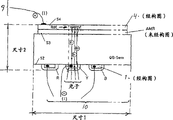
At first will use the enforcement of a plane electronics reflector (PEE) the present invention to be done theoretic explanation with reference to figure 1 and Fig. 2.And, for clarity sake, under the prerequisite of not loosening theoretical validity and generality, will using the model of a simplification, this model will use the electrode of one group of special use.Should think that in no case this is a limiting factor of the present invention.Special configuration among Fig. 1 and Fig. 2 just is used for the purpose of graphic extension, has other more general and/or different configuration, must regard them as to be included within the present invention.
In Fig. 1, represent a simplification electronic band structure as the space coordinates function of a semiconductor or insulating material, indicate that wherein quantum mechanical can Ev (top of valence band) and Ec (bottom of conduction band) to two the closest places of electric transmission relation.These two ENERGY E v and Ec are separated by a band gap Eg.One group of two metal electrode of deposition on two surperficial S2 of correspondence of described semiconductor or sheet of insulation and S3, negative electrode 1 and anode 4.For simplicity, suppose that these two electrodes are identical.
Under the Kelvin zero degree, the above chemical potential energy (μ with metal electrode of all Ec
M Ch) above quantum mechanical electronic state be blank, the chemical potential energy (μ of the following and metal electrode of Ev
M Ch) those following states are occupied.Certain determine temperature for example under Kelvin 300 degree with hot dynamic equilibrium under, suppose described semiconductor or the insulating material chemical potential energy (μ in essential part
B Ch) in somewhere near the band gap centre.For simplicity, suppose that this chemical potential energy (on energy) is identical with the chemical potential energy of metal electrode, so just form one and be called neutral electrically contacting.Under this determines temperature, a little and definite activity electron density n will be arranged at ENERGY E c place
e, and a little and definite activity hole density n will be arranged at the Ev place
hAnd supposition half classical approximatioss is effective, this means when applying external electrical field E not change partly in the electronics band structure.Because the existence of classical electromotive force, this effect of electric field by whole quantum mechanical at given distance X place can the suitable energy excursion relevant with the space calculate
V(X)=E·X (1)
Therefore Fig. 1 is described in and determines the situation when not applying external electrical field under the temperature.
When adding on the metal electrode 1 that a definite negative electrical charge changes Δ Q simultaneously when metal electrode 2 is removed corresponding negative electrical charge and changed Δ Q, the situation that Fig. 1 describes will become the situation that Fig. 2 describes.These additional charge on two described electrodes will cause existing a constant electric field E in described semiconductor or sheet of insulation.At low ohm electric field E (about 100V/cm; Also referring to Fig. 2) under, mobility and hot electron density n
eWith hole density n
h(Fig. 2) will keep substantially constant, and their migration velocity will change correspondingly
Vdrift (electronics; The hole)=mobility (electronics; The hole) E (2)
Electric current I separately
eWith I
h(Fig. 2) increase along with applying increasing of electric field E in this way.Current component I
Bal(Fig. 2) the accurate ballistic electron of influence is by the total current of structure shown in Fig. 2, accurate ballistic electron is those electronics of injecting described semiconductor or insulating material from metal electrode 1, when it along accurate trajectory track shown in Figure 2 by described semiconductor or insulating material when metal electrode 2 moves, do not have non-resilient loss to change basically without any tangible momentum yet.Current component I
EmFormation be because those electronics (accurate ballistic electron), they still have enough energy (this energy is greater than the energy barrier at emitting surface S4-free space interface) and enough big velocity components along directions X after passing described semiconductor or insulating material from metal electrode 1 and entering metal electrode 2, thereby can escape into free space (FS Fig. 2) by electron emitting surface S4 (Fig. 2) from added the structure that the above semiconductor or insulating material add that metal electrode 2 is formed by metal electrode 1.
QB-Sem
The preparation in each zone of the accurate ballistic electron transmitter/reflector of explanation now.
The preparation of a high ohmic semiconductor or insulator will be described now with reference to figure 3.In this case, accurate ballistic semiconductor (QB-Sem) is described monocrystal silicon sample, and it is held in both hands from a monocrystalline silicon of making through the float-zone crystal growth method and downcuts.Thin slice (wafer) is from then on held in both hands cutting-out, have perpendicular to wafer surface<111〉crystal orientation.But, also can select other<110〉have identical result with<100〉crystal orientation.If the crystalline material beyond the use silicon should select to be suitable for the crystal orientation of this crystalline material.Surface S2 and S3 pass through optical polish.The doped level of phosphorus (given n N-type semiconductor N) elects 2.0 * 10 as
12Cm
-3Make a Schottky contacts (negative electrode) by on surperficial S2, evaporating the thick gold of evaporation 200nm (2000 ) that the thick chromium of 5nm (50 ) continues one by one.Anode is an ohmic contact, comprises the rotten silicon layer (the thick thin district of about 1 μ m, below surperficial S3-referring to Fig. 3) of high phosphorus density, with the golden film of the thick evaporation of one deck 15nm (150 ).
The accurate ballistic semiconductor of zone 2-
The selection of accurate ballistic semiconductor is not limited to a kind of specific material, and can use different materials to prepare with many diverse ways.Unique requirement is the accurate trajectory track that has a definite band gap Eg (referring to Fig. 1) and have electronics between the opposite sides of material.At material described in the most preferred embodiment (QB-Sem) is silicon, but the 111-V of family composite semiconductor (for example gallium arsenic) is the confession selection material of getting well with the 11-VI of family composite semiconductor too.When selecting a suitable accurate ballistic semiconductor, the working temperature of the doped level of crystal orientation, deep layer and shallow-layer and the device that completes is the important parameter that should consider.Insulator is SiO for example
2, Al
2O
3, carborundum, silicon nitride, diamond (or diamond-like carbon particle) and other be suitable as accurate ballistic semiconductor (at least on principle) too well.Or studied about some material is used as field emitting electronic source (referring to prior art).
In the most preferred embodiment that Fig. 3 describes, cathode zone forms by the metal film of evaporation chromium on the surperficial S2 of silicon sample or gold, forms the Schottky contacts of a rectification with the method.The sole purpose of cathode zone is the negative electrical charge Δ Q that keeps the various quantity on the surperficial S2, and this can realize by many diverse ways.
In such alternative method, zone 1 is for example argon and a nitrogen of a gas phase part ion oxidizing gases.Do not need metal electrode in this case fully.
For obtaining the optimum performance as the negative electrode of the electronics injection utmost point of electronics being injected QB semiconductor regions (2 among Fig. 3), requiring (increases and injects the semi-conductive electronics of QB) mobile chemical potential energy μ as much as possible from the described additional negative electrical charge Δ Q of storage battery (referring to Fig. 3)
M Ch(referring to Fig. 2).This can reach reduction interface electron density state by surperficial S2 being carried out machinery, chemistry and/or heat treatment.If desired or require metallic cathode, this processing of surperficial S2 should be carried out before deposit metallic material.Perhaps, can select a kind of have the low electron density state under Fermi level and the metal material of low electronic work function.
As mentioned above, the phosphorus of high dose has been injected in the thin district of a silicon sample that is close to surperficial S3, goes bad by the method.On described surperficial S3, deposited the thin golden film of one deck (surperficial S3 is through optical polish before deposited gold film) then, made total form a ohmic contact silicon sample with the method.The making of this anode region may not produce the optimum performance of described plane electronics reflector PEE.
As cathode zone, the sole purpose of anode region is the negative electrical charge Δ Q that guarantees to remove from the various quantity in surperficial S3 zone.Here, the requirement about described (anode) regional best-of-breed functionality effectively requires different with the target zone.Hole current I
h(referring to Fig. 2) should be as far as possible little (as surface chemistry potential energy μ
M ChElectric current I when moving down
hIncrease), the thickness of metal anode also should approach (when accurate ballistic electron has big relatively energy loss 4 the time by regional) as far as possible.For realizing first target, in 4 interfaces, surperficial S3-zone, need one to have the high electron density state under Fermi level and the metal of very high electron density state.As making to surperficial S2, here equally can by before plated metal to described surperficial S3 carry out suitable machinery, the chemistry and/or heat treatment realize.
For realizing second target, can select another possible alternative.In the case, surperficial S3 does not have metal electrode (zone 4 among Fig. 3) and is placed in the free space FS (Fig. 3) an additional electrode (electronics intensifying ring 7-is for example referring to Fig. 8) and adjacent surperficial S3.This interpole with respect to surperficial S3 with/or cathode zone be biased under the relative high positive potential, whole device polarizes in this way.If the electric fields of setting up in the zone 2 are not enough to the accurate ballistic electrons in the zone 2 are accelerated to have make these electronics escape into the energy of the needs of free space FS by described surperficial S3, can with surperficial S3 with such method geometrical figuration make some spikes of on the space of surperficial S3, approaching electronics intensifying ring 7 among Fig. 8 most (with/or rapid bending area) locate to increase partly described electric field.
At last, an available thin metal electrode (as anode) covers the surperficial S3 of geometrical figuration, and whole plane electronics reflector assembling (comprising electronics intensifying ring 7) seems as the layout of representing among Fig. 8.Arrange that with this effect that discharges and recharges on surperficial S3 that makes geometrical figuration reduces to minimum.
Here the emphasis that will emphasize is that the shape of electronic emitter surface S3 (if existing metal electrode 4 to be surperficial S4) needs not to be strict plane.
The performance of QB-Sem
Sample is placed in the vacuum between negative electrode and the anode and is under about 4.0V external voltage (forward bias) and (applies under the situation of 4.0V in 0.5 μ m silicon sample thickness range, in the silicon sample essential part, set up the electric field of 80.0V/cm), can be observed definite, big relatively and a horizontal electron emission current I uniformly
EmEmission current I
EmAmplitude indicate about 30% of whole electronics to inject silicon sample from negative electrode, arrive the anode that has about 4eV energy (electron affinity energy is 4.0eV in the silicon) more than the ENERGY E c (referring to Fig. 2), be enough to make these electronics to overcome the energy barrier of anode surface S4-vacuum interface and escape into free space FS (referring to Fig. 3).
Practice explanation of the present invention
At first will use a plane electronics reflector (PEE) from putting into practice the present invention to be described with reference to figure 3, Fig. 3 is the schematic diagram of a graphic extension according to one of most preferred embodiment of the present invention possible physical model.
Zone 1 (negative electrode) passes through surperficial S2 join domain 2 (an accurate ballistic semiconductor), and connects external charge/voltage source 8 (batteries) by female electrical contact (ECP).Its (negative electrode) is to supply with and keep negative electrical charge Δ Q (electronics) on the surperficial S2 together with the effect of battery.Simultaneously, remove the negative electrical charge Δ Q of equivalent from zone 4 (negative electrodes).Anode passes through surperficial S3 join domain 2, and connects the positive pole in external charge/voltage source 8 by ECP.Described electron source is kept the just charging of surperficial S3.Between surperficial S2 and S3, set up a uniform electric field E with the method, cause a definite electric current I
TotFlow through zone 2.Referring now to Fig. 2,, this electric current I
TotComprise 3 current component I
e, I
hWith I
EmPreceding 2 components form background current I
Back, and component I
EmBy that part of electronics (being called accurate ballistic electron from now on) if-have a sufficiently high electric field E and corresponding potential difference (V=Et1) to remain between surperficial S2 and the S3, they leave device and freedom of entry space FS (Fig. 3)-formation according to physical laws.
When a block semiconductor or insulating material (regional 2-is called QB-Sem from now on) through suitably preparation, surperficial S2 and S3 through suitably handling zone 1 and zone 2 through suitably selecting when constructing current component I
Em(electron emission current) can become with respect to background current I
BackQuite big.
When the QB semiconductor is suitably selected and is prepared, at this moment make great efforts (comprising the optimization of surperficial S2 and S3) even without any optimization, at the gross thickness L2 of device is under the situation of naked eyes visible (less than several mm), under the electric field (being called an ohm electric field from now on) of about 100V/cm order of magnitude, can measure the Iem of every square centimeter of hundreds of nanoampere.Length dimension L1 (square root of device area) with the 30cm order of magnitude (for example present die size), the device of describing among Fig. 3 is a large-area planar electronic emitter, its manufacturing is very simple, and can under the ten minutes competitive price, produce, even same standard cathode ray tube (CRT) screen is compared.
In the most preferred embodiment of in Fig. 3, describing, by supplying with the negative electrical charge Δ Q of extra quantity to metal electrode 1 (negative electrode) from battery, realized on electric one fully the electronics from negative electrode to silicon sample inject (electric charge inject-referring to Fig. 2).Yet because semi-conductive electronics injects also relevantly strongly with temperature from cathode zone to QB, therefore plane electronics reflector alternate embodiment according to the present invention can comprise the cathode construction (regional 1-is referring to Fig. 3) of a heating.In another alternate embodiment, electronics injects the QB semiconductor by optical illumination cathode emission S2 zone, surface (this zone can comprise a part of QB semiconductor of abutment surface S2 in some cases) through surperficial S1.This embodiment of flat emitters PEE according to the present invention is particularly useful in light-electronics charging.These electronics injecting methods will illustrate in the description to relevant most preferred embodiment during each saves below.
Illustrate according to plane electronics reflector of the present invention (PEE) by describing the most preferred embodiment of representing among a Fig. 3 now.But also have other embodiment in a large number, all according to the present invention, they relate to the different choice of material, design, making and the structure of described plane electronics reflector, and described difference depends on the requirement of using on hand.Should emphasize that though electronics is injected the free space of the PEE that is used to illustrate the semiconductor-based present principles of QB, this is not a requirement.Other possible embodiment will show as some, the semi-conductive fundamental characteristics of QB, and the accurate ballistic transport of electronics can be improved many non-emission semiconductor device equally.
Applicating example (most preferred embodiment explanation)
Referring now to Fig. 3 to Figure 24 graphic extension with discuss except that the plane electronics reflector according to many application of the present invention.Although will with relevant drawings each application and product be described by a special implementing example, and at this moment must emphasize to use the generality of each application of the present invention.For each such most preferred embodiment, exist a large amount of other embodiment and the modification of this most preferred embodiment, they all use the present invention as a conclusive part.Therefore, should not see restriction to what in former joints, provided as to the explanation of the present invention and the explanation to application of the present invention that will provide in the back to the present invention and application thereof.This understanding is basic.
Example 1. Field Emission Display (FE-FPD)
One of the present invention significantly to use be the structural member that is used for firm, reliable, large-scale, low-power consumption and the Field Emission Display (FE-FPD) of cheapness.
Fig. 4 along the cutaway view of the A-A line of the FE-FPD that represents among Fig. 5, is according to one of possible no vacuum FE-FPD of the present invention promptly.Referring to Fig. 3, basic planar structure-1 of the present invention (negative electrode), 2 (QB-Sem) and 4 (being optical transparency in anode-this most preferred embodiment) are same clear the demonstration in Fig. 4.Unique negative electrode and anode of not being both in this flat panel display applications of the present invention introduced an additional thin layer 3 through composition and between semi-conductive surperficial S3 of QB and anode 4.This 3rd thin layer comprises redness 5 that (through composition) for choosing form by fluorescent material or other colorful light-emitting body, yellow 18 and blue look 11 sections.These sections are isolated from each other by means of non-luminous Electron absorption material 16.
Typical overall size L1, the L2 of " single-chip " FE-FPD that describes among Fig. 4,5,6 and 7 under the silicon wafer situation that can utilize diameter for 30.0cm, take advantage of the 20cm order of magnitude for 20cm at present.When the big color monitor of needs, " single-chip " assembly of a random number can combine on a suitable substrate, utilizes section d2 and d4 (referring to Fig. 5) as the land, prevents that with the method the space of the light image quality that forms is rotten.The thickness L3 of the described FE-FPD that describes among Fig. 4,5,6 and 7 is the 1mm order of magnitude, and this thickness is exactly the thickness of QB semiconductor wafer basically.
In Fig. 6, thin layer 3 and 4 by changing-over so that the another kind of possible physics pattern of the described FE-FPD of graphic extension.Here colored hair photosphere 3 is directly towards free space FS.If desired, surperficial S5 can comprise the protection coverage of transparent (antireflection).Here must emphasize that the section 5,6 and 11 of expression not necessarily must be a luminous element among Fig. 4,5,6 and 7.Colored hair photosphere 3 is also represented material and the device of other type electronics to the colourama conversion.Such type can illustrate layout by Fig. 4.In the case, structure 1 (negative electrode), 2 (QB semiconductor), redness/yellow/blue color component (5,18,11) form a colorful light-emitting diode (CLED) matrix with 4 (anodes).Other FE-FPD arranges also can use the present invention certainly, and never the most preferred embodiment of expression among Fig. 4,5,6 and 7 should be regarded as a restriction to the range of application of the present invention in this application.
At last, use under the present luminous element and the unappeasable situation of other electronics-light conversion element/equipment on hand in the requirement of color-resolution, brightness and color contrast, may still need to adopt the quite high electron energy of the requirement standard TV color fluorescence material of (the interior high accelerating voltage in zone is about 10 to 20kV).One is used the present invention, is illustrated in solution and a possible physical model that vacuum field emission flat panel display among Fig. 7 may be still a best.
In this is arranged, Fig. 4,5, with 6 in the colored hair photosphere 3 of expression from the removal of basic plane electronics emitting structural 1 (negative electrode), 2 (QB semiconductor) and 4 (anodes) and be deposited on the optical transparency plate (for example glass) 13, this plate with part 14 with 12 Vacuum Package that constitute described vacuum FE-FPD.The electronics intensifying ring 7 that is deposited on the luminescent layer 3 biases to suitable high positive voltage.This arrange to guarantee to leave the accurate ballistic electron of basic electronic plane trigger mechanism (being mechanically anchored on the base plate 12 by mechanical support 15) by surface 54 and is accelerated in free space FS (now being vacuum) and has sufficiently high energy, so that the correct work of assurance standard colour TV fluorescent material 5,6,11.
The thickness of the vacuum FE-FPD that represents among Fig. 7 (Dim2-size 2) is 1 to the 2cm order of magnitude, and area (Dim1-size 1) is constant with respect to previously described no vacuum FE-FPD.
Example 2. plane electronics bundle photoetching
By using plane electronics reflector according to the present invention to solve the major defect that the short life by prior art plane electronics reflector brings.The present invention need provide qualitatively novel and a robust solution for modern times of semi-conductor industry.The method and embodiment are illustrated among Fig. 9 to 14.
In the prior art, used Fig. 8 to describe plane electronics bundle photoetching principle schematic.In prior art joint, used the plane electronics reflector of prior art that the projection system of an electric lithography has been described.Plane electronics reflector of the present invention can directly be implemented to replace the reflector of prior art.
Be illustrated among Figure 10 according to one of this plane electronics emitter structures of the present invention possible embodiment.It is to have replaced a film oxidation layer 24 among Fig. 8 with one among Figure 10 accurate ballistic semiconductor GB-Sem with the main distinction of prior art Fig. 8.Turn over now to Figure 10, annotate the semi-conductive electronics of QB from negative electrode 1 by surperficial S2, along the accurate trajectory track transmission in the QB semiconductor.They enter absorption template 19 or anode 4 through composition by surperficial S3.The accurate ballistic electron of a part is not stoped by Electron absorption template 19, at this moment has enough energy with freedom of entry space FS, for example electronics on the i point by surperficial S4.These electronics are accelerated to by electronics accelerator card 7 in the FS of free space zone then has sufficiently high energy.Electronics accelerator card 7 is deposited on the responsive resist layer 6 of electronics in this special wafer legend.
By electronics-light method, for example the electronics that occurs at an i (Figure 10) is mapped into the some j that is in the resist layer 6.Sequentially be transferred on wafer-resist assembly with the situation of the whole photoengraving pattern of the method (layer 19) in the time of can shifting rather than resemble with the photoetching of standard electronic bundle simultaneously.And, the not basic restriction of the lateral dimension of patterned layer 19, and this means and can in once exposing, handle entire wafer.If optimization of electronic-photosystem is together with 1: 1 electron projection stepper of plane electronics emitter element, available minimum details (" Mins-is minimum ") is much smaller than 0.15 μ m.In addition, expose simultaneously by entire wafer, the quantum of output that makes the photoetching of this plane electronics bundle is very big.Other layout of many plane electronics photoetching can be arranged, and the layout of representing among Figure 10 is one of them.
The possible replacing representation of the embodiment that represents among Figure 10 is in Fig. 9.Referring now to Fig. 9,, clearly illustrate one with discussion referring to Figure 10 in identical accurate substantially ballistic electron emitter structures.In the specific most preferred embodiment of in Fig. 9, representing, an accelerator card 7 and electron flare device 17 structures are inserted in plane electronics emitter structures 1,2,19,4 and wafer adds between light-resist part 6.This layout makes the plane electronics projection system can be in vacuum (Vacuum Package of the described electronic emitter structures that zone 17,12 and 14 constitutes) time continuous operation (if necessary), and pending wafer can be placed on scintillator 17 above.Provide better a electric transmission at vacuum work, and emptying in advance, increased the quantum of output of entire device from emitting surface to wafer.If the air gap of indicating among Fig. 9 is enough little,, can reduce the size of minimum details " Min-minimum " owing to can keep scattering of light minimum.
Publication (the H.Ahmed et al: " micro-lithography discussion collection of thesis " that writes by inventors more of the present invention that in prior art joint, mentions; Cavendish laboratory, Cambridge 1989) in, in Figure 11,12,13 and 14, indicate and experimental demonstration how to carry out the photoetching of plane electronics bundle in practice.Disclose a device " experiment with 1: 1 electron projection stepper ", and clearly proved the whole industrial needs and the requirement of the satisfied lithography step about IC production period needs of its performance.Its schematic is shown among Figure 11.Here 20 is described negative electrode-QB-Sem-anode assemblings (quite similar with the part in the arrangement of representing among Figure 10 1,2,19 and 4), the 6th, have the wafer substrates that deposits resist layer, the 21st, X, Y position desktop, last 22 is a pair of Helmholtz coils of setting up uniform magnetic field between K-A assembling and wafer-X, Y desktop assemble.In this special layout, negative electrode-QB-Sem-anode assembling is a negative bias with respect to wafer substrates, and wafer substrates keeps closely current potential.Electrons emitted is quickened to ground from high negative potential in the electric field of setting up.Parallel electric field and magnetic field form 1: 1 electronics-light projection system with the method, the electron transfer that occurs from a specified point on the lower surface of negative electrode-QB-Sem-anode assembling 22 to the interior single-point (referring to Figure 10) of resist layer 6.
Described experiment is illustrated among Figure 12 with total figure of 1: 1 electron projection stepper, and the experimental result of some wafer compositions is illustrated in Figure 13 and 14.Tested positive with negative resist, under the situation of typical exposure time of 0.1 second order of magnitude, the minimum details that can easily obtain (size among Fig. 8 " Min-minimum ") is in 0.15 mu m range (Figure 13 and 14).Represent a whole part that is exposed with composition (test composition repeatedly) silicon substrate among Figure 13, represented the detailed structure of test composition among Figure 14, clearly proved the minimum details ability of 0.15 μ m of this prototype instrument.
Example 3. two-dimentional illuminatian plates
Because according to simple in structure, sturdy and durable, the low-power consumption of plane electronics reflector of the present invention, low working temperature and two-dimensional nature, described plane electronics reflector can be advantageously used in the light source of two dimension (plane and on-plane surface).
A this possible illuminatian plate schematically illustrates in Figure 15 and 16.Here the basic structure of plane electronics reflector (negative electrode 1, QB semiconductor 2 and anode 4 injected free space FS as plane electronics source (when applying a suitable voltage between negative electrode and anode) with electronics).These electronics are accelerated electrode 7 and quicken to go forward side by side into light-emitting layer 3 in free space.Can make the Vacuum Package of the luminous energy of generation from the whole assembling of optical transparency plate 13 (being generally glass plate) (together with plate 14 and 12) formation of described structure effusion.
In another possible layout, omitted light-emitting layer 3 and be full of free space FS with suitable gas and admixture of gas, at this moment produce the illumination that needs by gas ionization and fluorescence.The typical sizes of above-mentioned flat illumination plate is pointed out in Figure 16." Dim1-size 1 "-illuminatian plate thickness can be easily below 1cm; " Dim2-size 2 " can easily be the m order of magnitude.
Because simple in structure, the present invention also can be used in the two-dimentional light source structure of on-plane surface (figure).A possible layout of this light source schematically illustrates in Figure 17.Here, negative electrode 1, QB semiconductor 2 are concentric cylindrical layer with anode 4.The QB electronics is radially injected free space FS, and after quickening through accelerator card 7, they enter light-emitting zone 3.Luminous light is overflowed by transparent (glass) shell 13.In this arranges, also can omit luminescent layer and be full of free space with suitable luminous gas.
Example 4. semiconductor elements and device
To only provide briefly introducing of some the typical case application of a present invention in semiconductor element/device and integrated circuit manufacturing field below, these must only be looked at as several case illustrated, and never they should be seen as a restriction to the application of the present invention in this area that relates to.Example to be enumerated is selected from the semiconductor element/device that can use 4 different main types (A to D) of the present invention.
In these examples, keep basic structure of the present invention (negative electrode, QB semiconductor and anode), although only utilize in some applications accurate ballistic electron between two electrodes characteristic and do not utilize them to escape into the ability of free space FS (referring to Fig. 2).Title " negative electrode " will always not be to use to attempt to use more the term of semiconductor physics with " anode ".The semi-conductive electron transport property of these QB with in the vacuum tube between negative electrode and anode the characteristic of ELECTRON OF MOTION quite similar, do not need vacuum only now.At room temperature produce and the whole equipment discussed can be made into submicron-scale from the electronics of cathode emission.Combine all advantages of vacuum tube and whole modern solid-state semiconductor technologies with the method the present invention.
Example 4A
Category-A: rectification and electric charge (information) are stored
This based semiconductor device/device comprises bipolar p-n, p-i-n diode, transistor and many unipolar devices, MIS (metal-insulator semiconductor (MIS)) diode for example, CCD (charge coupled device), the MIS tunnel diode, the MIS switching diode, IMPATT (impact avalanche and transit time) diode and BARITT (potential barrier injection and transit time) diode and other relevant transit time device.
Example: accurate trajectory Schottky diode
Figure 18 be one according to a typical quick plane Schottky barrier diode of the present invention.Also shown the equivalent RC circuit 36 and 37 (referring to US5627479 and EP672257B1) of describing a prior art diode 36 and a QB semiconductor diode 37 among the figure.
Referring now to Figure 18,, diode current I
DiodeExhausted resistance R d and control, and Rd is by depletion region W
dExtension determine.This depletion region length (width) W
dThe voltage Vso exponent function relation that applies between electrically contacting with Schottky.By controlling W by Vso
dObtain rectified action, thereby cause the strong variations control diode current I of the exponential relationship of Rd successively
Diode(forward and reverse diode current).Owing under high electric field, do not have velocity of electrons saturated, thereby in frequency applications, do not need to reduce the front of overall size L, especially depletion region and distance L so between the ohmic contact.According to accurate trajectory Schottky diode of the present invention can work under the upper frequency and it is characterized in that can by Figure 18 37 in R in parallel
QbWith L
Qb(dynamic inductance of accurate ballistic electron) and better simply structure and very low power loss arranged.
Example 4b
Category-B: photosensitive and luminescent device
This based semiconductor device/device comprises LEDs (light-emitting diode), photodiode, semiconductor laser, avalanche diode and be used for light other photoconductive device to the conversion of signals purpose.
Example: accurate trajectory photodiode and accurate trajectory light-emitting diode
The energy band diagram explanation of a simplification of expression among Figure 19 is according to the physical principle and a possible structure (most preferred embodiment) of an accurate trajectory photodiode of the present invention (A-mark), an accurate trajectory light-emitting diode (B-mark) and a first order input/amplification/space amplifying device (C-mark).Below these devices will be discussed successively.
Accurate trajectory photodiode (process A among Figure 19)
Light signal (entering light) is absorbed in cathode zone, and (zone between surperficial S1 and the S2-Figure 19) and a thin zone that is positioned near the QB semiconductor of surperficial S2 form many electron-hole pairs (process of mark among Figure 19 " Exc1 ") with this process.The electronics of light stimulus forms accurate trajectory current Ib al then, is accelerated and enters avalanche multiplication zone AMR by surperficial S5.Avalanche multiplication process AM causes an amplified current signal I
eWith I
hCan omit avalanche multiplication zone AMR in some applications, fully be amplified by the acceleration of the accurate ballistic electron that produces from the signal of telecommunication (" Exc1 ") of photon-electronic switch.
Accurate trajectory photodiode according to the present invention has high quantum efficiency and relative very low power loss, thus when need two-dimentional light images (signal) detect when handling can a two-dimensional light sensor array the form manufacturing.
Accurate trajectory light-emitting diode (process B among Figure 19)
Under the light-emitting diode situation, the signal of telecommunication (bias voltage between negative electrode and the anode) but also time modulation (light-electronic application) if desired, the electron injection quantity (process among Figure 19 " Exc2 ") that control enters QB semiconductor regions QB-Sem.After quickening, when by the QB-Sem regional movement, these electronics (electric current I among Figure 19
Bal) enter light-emitting zone (LER) and form photon stream (referring to the process B among Fig. 2 and Figure 19) by the process that reconfigures of crossing over band gap Eg by surperficial S5.This photon stream (if K-A AC bias voltage Δ Q (t) is relevant with the time, but also the time modulates) injects free space FS at last.
When electronics injection process " Exc2 " has sufficient intensity and light-emitting zone LER (P that normally attaches most importance to doping) when satisfying the necessary condition of population inversion, above-mentioned device will play accurate ballistic semiconductor laser, have low-power consumption, high efficiency and can very be used for light-electronic application, for example fiber-optic signal transmission and telecommunication effectively usually.
Light image detects and handles (process c among Figure 19)
In some applications, handle the accurate trajectory electric current I that forms by process " Exc1 " and process " Exc2 " in electronics-light mode
BalTo be necessary with/or favourable.In this case, the zone between interface S5 and the S3 just in time is the extendible portion of accurate ballistic semiconductor zone QB-Sem, as shown in Figure 19.After passing anode region, these accurate ballistic electrons are injected space FS as the electron emission current I that can carry out electronics-optical processing by surperficial S4
EmAmong the example 4d such device will be described.
Example 4c
C class: amplify and permanent memory
The application of the present invention in this based semiconductor device/device also comprises bipolar transistor and bipolar unijunction transistor, together with many unipolar components and device, comprise EFTs (metal-semiconductor field effect transistor, MOSFETs (mos field effect transistor) and permanent memory.Related especially with the present invention in this type of is tunnel transistor, TEDs (transferred electron device) and other trajectory (hot electron) transistor AND gate/or device.
Example: accurate ballistic transistor
Figure 20 is a typical planar metal semiconductor field effect transistor (MESFET) schematic diagram.Electric current I between source electrode and the drain electrode
dBe subjected to voltage V
gBy changing effective width of depletion region W
d(V
d) control." a " is the electric live part of substrate semiconductor SEM, and " L " is conducting channel length, and " L " is the width of device.When requiring quick performance, channel length must be enough shortens (<1.5 μ m) and typical operating voltage V
DsSet up the high electric field between source electrode and the drain electrode.At this moment electric charge (electronics) speed becomes saturated (reaching the mobility scope relevant with electric field), and this will limit the operating rate of described device.
For make discuss simple and clear for the purpose of, even the transistorized geometry designs of described MESFET as shown in Figure 20 keeps identical, when this mosfet transistor is constructed by the present invention, 2 design constraints above-mentioned (little physical dimension and velocity of electrons are saturated) will not exist.The device that provides as shown in Figure 20 constitutes, and this comprises the Semiconductor substrate Sem (referring to Figure 20) that is replaced standard merely by accurate ballistic semiconductor QB-Sem.
According to the present invention and the MESFET device of representing in Figure 20, its feature not only is quick response (high frequency response), and is very low power loss, the trajectory character because source electrode-drain current Id is as the criterion.
Here must emphasize once more that the transistorized project organization of the MESFET that represents among Figure 20 is in amplifications/switching device a large amount of possible just.Because character of the present invention, other better design is possible and should be appreciated that these designs will absorb some design feature of vacuum tube (referring to the 1237th page of the publication of above-mentioned K.W.Boer).
For in this type of according to the structure of mos field effect transistor of the present invention (MOSFET), permanent memory MOSFETs and other device, have and top identical and/or quite similar argument during the MESFET transistor is discussed.All these devices are characterised in that simplicity of design, sturdy and durable, high response speed and very low power loss.
Example 4d
D class: the detection of light image, formation and processing
Because two-dimensional nature of the present invention can carry out detection, conversion and the processing of large-area light signal.With the electromagnetic field radiation is example, and the present invention can be used for many aspects:
The signal of telecommunication (electrographic light image) of record is changed back two-dimensional image/signal (accurate ballistic semiconductor Field Emission Display-referring to example 1).
Two-dimentional light image is converted to the signal of telecommunication (accurate ballistic semiconductor gamma camera).
The two dimension light image detects, and the signal of telecommunication amplifies as a result, amplifies and last two-dimentional light image record succeeded by two-dimentional light image space.The result that this light image is handled is still original two-dimentional light image, but contrast is amplified and amplify in the space.
During detecting, form at light image and handle, latter two aspect all uses the two-dimensional detection array of electromagnetic field radiation.This comprises can be defined as two basic application of the present invention roughly:
A) accurate ballistic semiconductor gamma camera (two-dimentional light image/signal is to the conversion of electrical signal sequence).
B) brightness/contrast that is used for two-dimentional light image/signal is amplified the system of amplifying with the space.
To narrate in this section QB semiconductor gamma camera a) with light image/signal processing b) a brief description.For simple and clear for the purpose of, when these two of explanations are used, suppose that light signal takes by the two-dimensional image form that forms from the photon in the visible part of Spectrum of Electromagnetic Radiation.In any case certainly can not regard this supposition as in this type of is used, use a limiting factor for the present invention and its.The light signal of to be detected/processing is probably by forming from the photon in the other parts of Spectrum of Electromagnetic Radiation, and it also may be a signal that is formed by other particle.The bulk of light image also can from 0 to 3 variation.At last, provide the feature of 2 example application of the present invention below, be used for explanation/instruction purpose purely, can not regard them as a limiting factor that the present invention is used in this field.
A) accurate ballistic semiconductor gamma camera
Figure 21 be one according to a schematic diagram that is used to detect and write down two-dimentional light signal/image device of the present invention.In this most preferred embodiment, the QB semiconductor is clipped between negative electrode 1 and the anode 4.2 electrodes are all by the method composition that is similar to the X shown in Fig. 5, Y composition.Metallic cathode, QB semiconductor and anode constitute the two-dimensional array of a Schottky barrier photodiode, it can by seriatim with addressing sequentially, (pixel diode i, j-connects) as shown in Figure 5.
Light image forms around surperficial S2, through conversion and processing, by means of described device, determine the sequential of the signal of telecommunication with following method: the light image that forms light (electronics) enters described structure that Figure 21 represents by suitable colour filtering R (redness), Y (yellow) and B (blue look), be absorbed in then in the zone that comprises negative electrode-QB interface and QB semiconductor depletion region, in this process, produce many electron-hole pairs.
By between cathode strip " i " and anode strap " j ", applying specific pixel diode (i of suitable voltage " connection ", j) (diode that has yellow filter " Y " among Figure 21), the accurate ballistic electron that produces is accelerated in QB semiconductor regions QB-Sem (Figure 21), and can further be amplified by the avalanche multiplication effect in the avalanche multiplication zone AMR (Figure 21) if necessary.The current impulse that obtains thus forms electronic signal, and (i, j) luminous intensity of " yellow " photon on is relevant at the pixel shown in Figure 21 with collision for this electronic signal.
The gross thickness (Dim2-size 2) of described device (QB semiconductor gamma camera) is in several mm scopes, and the effective area of described device (lateral dimension Dim1-size 1) can reach about 30cm order of magnitude under modern technologies.High-quantum efficiency, high spatial resolution, the several attractive characteristics of the device of proposition according to the present invention just sturdy and durable and simple in structure.
B) light signal/image processing device
In many application (for example do not have historical relic Neo-Confucianism, infrared imagery and other), must detect, handle and write down very faint two-dimentional light image, and have about high spatial resolution/amplification and about the additional requirement of extractible spectral information.Satisfy schematically illustrating in Figure 22 of these requirements according to one of possible device of the present invention.It comprises two parts, and part A is two-dimentional light image/signal amplifying part branch, and part B is the space amplifier section of two-dimentional light image/signal.
In primary light image plane 25, form entering in the zone that photon is absorbed in negative electrode, interface S2 and QB semiconductor depletion region of light image,, produce many electron-hole pairs with the method as schematically illustrating among Figure 21.Its number depends on energy (spectral information) that enters photon and the number (signal strength information) that enters photon.The accurate ballistic electron that produces in the primary light image plane is accelerated (once amplifying) in QB semiconductor regions QB-Sem, and since their characteristic they can leave basic plane electronics emitter structures (negative electrode, QB semiconductor and anode) by surperficial S4.Meanwhile they form the electronics-light image of a primary light image equally in the primary light image plane with the method.
This photon to the conversion of electronics (photon enters-electron hole pair output) with once amplify (electronics of generation quickens) afterwards in the QB-Sem zone, the electronics-light image that forms in the plane of surperficial S4 that obtains can be for further processing by suitable electron lens (not shown).It further amplifies (secondary amplification) by means of accelerating electrode, and if necessary, also can carry out the space and amplify (electronics-light primary space amplifies).
This amplifies the electronics-light image that amplifies with luminous intensity and back is converted to the secondary light image by a suitable electron flare device 17 through the space.The plane 26 of this secondary light image becomes the objective plane of last optical amplification system 29 to guarantee the quadratic space amplification of primary light image then.The last light image that amplifies through signal/intensity in part A and amplify through the space in 29 in the end forms on the light image plane 27, is ready to carry out record by suitable optical recording device 28 (videotaping plate or CCD).The spatial resolution that depends on requirement, whole assembling (part A and part B) can laterally be moved in the primary light image plane.
Should point out at last because the characteristic of the basic plane electronics reflector of the part A bottom of formation device, described plane electronics reflector partly can be used as a spectroscopic device together with the electronics-light in the FS of free space zone, extracts the necessary information about photons spectrum in the initial light image.
Example 5. photovoltaics are used
Because accurate ballistic electron inelastic scattering seldom and very low combination rate again, Schottky barrier diode according to the present invention is a kind of photoconductor efficiently, and its purposes in photovoltaic is used is conspicuous.Schematically illustrate one of possible structure according to solar cell of the present invention among Figure 23.
Described device is clipped between 2 electrode-negative electrodes 1 and the anode 4 by QB semiconductor layer 2 and constitutes.Negative electrode constitutes a Schottky rectification with the QB semiconductor and contacts, and anode and QB semiconductor constitute an ohmic contact.When constructing with the method (using a P type QB-Sem), the electric charge that takes place because setting up dynamic heat balance shifts the internal electric field E (X) in the described device that causes, has the distribution pattern that Figure 23 lower part is represented.
(Figure 23) enters described device (according to solar cell of the present invention) and is absorbed in the structure by negative electrode daylight from the left side, and each photon that enters produces an electron-hole pair.The absorption process of separating on the space can be divided into 3 classes.Process D is the production process of the electron-hole pair at the interface between negative electrode and QB semiconductor.Process E is that the production process of electron-hole pair in the semi-conductive depletion region of QB and process F are described in and absorb the process that photon produces electron-hole pair in semiconductor-based this part of QB (internal electric field is 0 QB-Sem zone).Because at accurate trajectory track, the great majority of the special electronics that produces are with depleted district W in the semi-conductive depletion region of QB at the QB semiconductor memory
dIn the internal electric field anode direction that exists quicken and not again in conjunction with/or inelastic scattering.This effect has improved the quantum efficiency of described solar cell significantly.By making the live part scope extend minimum and suitable cathode material (for example tin oxide of electrically conducting transparent) the optimised devices structure of selecting, solar cell according to the present invention provides a conversion equipment with very high, simple in structure and robust light of efficient of big effective area to electric energy.
Example 6. electronics pop-up microscopes
Here be called electronics pop-up microscope (ECCM) and carry out in the field that defective in " mixing " semiconductor wafer and weakness detect a potential application crucial of the present invention being arranged using.Referring to Figure 24 this device is discussed.
In the electron emission microscope of standard, sample to be detected is heated to when thermionic emission and becomes temperature when determining.These electronics break away from sample by a surface, then through the electronic light image of electronics-optical processing with the part surface (injecting vacuum by its electronics) that forms a high spatial resolution.But, the information that can extract by this electron-like microscope about being detected sample be confined to the surface with just in time at subsurface several monolayer materials.This is because the mean free path of electronics (having enough energy to escape into vacuum) is minimum (much smaller than 50 dusts) under these conditions.
In the scheme that experimental technique according to the present invention proposes, leave the electronics of sample (the QB-Sem zone among Figure 24) by surperficial S3 and inject described QB semiconductor at surperficial S2 place, thereby they are loaded with information about sample state in the sample along their whole accurate trajectory track.Any blemishes and defective (these may be one dimension, two dimension and/or three-dimensional various ways) will cause the scattering (with the thermalization that then causes electronics) of electronics and leave their accurate trajectory track.This will produce the contrast of a projection-type on electronics-light image plane.
Schematically illustrate a microscopical possible most preferred embodiment of electronics pop-up according to the present invention among Figure 24.Same in this case reservation basic structure of the present invention (negative electrode, the QB semiconductor, anode-referring to Fig. 1 and 2), just at this moment described basic structure constitutes a sample to be detected.Inject the semi-conductive words of QB if can produce the electric field and the electronic energy of sufficient intensity in the QB semiconductor by surperficial S2, in fact not demand side to the metal electrode of QB semiconductor surface S2 and S3.Can contactlessly not mix the in this configuration overall process of defective quality control.These electron injection are along the accurate trajectory orbital motion of their straight line, and those will not injected vacuum by QB semiconductor surface S3 at last by the electronics of blemishes, impurity, defective and/or other irregularity deflection.The superficial density of these electronics, their energy and their emission angle be with accurate accurate ballistic electron with surperficial S2, with along the semiconductor-based this part of the QB of their tracks and with the relevant parameter of the interaction of surperficial S3 (quantity).
Handle through electronics that the section 32 of surperficial S4 is injected electronics-light image 33 by standard electronic lens 34 then with the high spatial resolution (through amplification) that is formed on described section electronics-light image plane 30 in.
By the QB semiconductor being placed on a high-precision X, the Y platform, can the method detect the standard resolution that entire wafer reaches 10 to 50 dusts of an exemplary scanning electron microscope.
Example 7. ordinary electronic electron guns
Though the present invention's's (plane electronics reflector) main target be need with/or the application of getting profit from the two-dimensional nature of described invention, feature of the present invention (for example low power loss, simple structure, high electron emission current density and working and room temperature) make the use of the present invention in the electron beam source of standard more equally very attractive.Can easily make the electron source of point-like, composition, directrix plane and common shape, here they are referred to as " cold schottky cathode ".Their typical use is the electron source as cathode ray tube (CRT), X-ray tube, electron microscope, comprises as evaporation, welding, the developing electron gun with possible other electron beam application.
Because all these application are looked at as common application of the present invention,, and in the prior art joint, describe again because they have been well-known.Therefore will not be described in a more detailed discussion here.
Claims (54)
1. an electron emission device comprises:
-one has first and second surperficial element, and wherein first surface is suitable for keeping a kind of first electric charge, and second surface is suitable for keeping a kind of second electric charge, it is characterized in that, this element also comprises separately this first and second surperficial material layer,
-being used to provide the device of the electric field that crosses at least a portion element, described electron emission device also comprises:
-provide the device of first electric charge to the first surface of element, with
-device of second electric charge is provided to the second surface of element, second electric charge is different with first electric charge, so that along be basically perpendicular at least first or the direction of second surface move a plurality of electronics by element, and the part in described at least a plurality of electronics is from this element emission
Wherein:
This material layer of-preparation so that by it being become have perpendicular to first or the monocrystal material of the predetermined crystal orientation of second surface, and is lower than 10 by having
14Cm
-3Impurity concentration, thereby reduce electron scattering in this material layer, wherein this material layer is a semiconductor layer.
2. according to the electron emission device of claim 1, wherein said material layer comprises the material of selecting by in silicon, germanium, carborundum, GaAs, indium phosphide, indium antimonide, indium arsenide, aluminium arsenide, zinc telluridse and silicon nitride or their group that any combination constituted.
3. according to the electron emission device of claim 1, the preparation of wherein said material layer comprises with a kind of dopant mixes so that obtain a predetermined impurity concentration to this material layer.
4. according to the electron emission device of claim 3, wherein dopant comprises phosphorus, lithium, antimony, arsenic, boron, aluminium, tantalum, gallium, indium, bismuth, silicon, germanium, sulphur, tin, tellurium, selenium, carbon, beryllium, magnesium, zinc or cadmium or their any combination.
5. according to the electron emission device of claim 1, wherein provide the device of first electric charge to comprise first material or the material system of conduction at least in part to first surface.
6. according to the electron emission device of claim 1, wherein provide the device of second electric charge to comprise second material or the material system of conduction at least in part to second surface.
7. according to the electron emission device of claim 5, wherein first material of conduction or material system constitute the layer with first and second surface at least in part, wherein first material of conduction or the second surface of material system effectively are connected with the first terminal of a charge reservoir at least in part, and wherein first material of conduction or the first surface of material system directly contact with the first surface of the material layer of element at least in part.
8. according to the electron emission device of claim 6, wherein second material of conduction or material system constitute the layer with first and second surface at least in part, wherein second material of conduction or the first surface of material system effectively are connected with second terminal of charge reservoir at least in part, and wherein second material of conduction or the second surface of material system directly contact with the second surface of the material layer of element at least in part.
9. according to each electron emission device in the claim 5,7, wherein first material or the material system of conduction comprise that metal or doped level are higher than 1 * 10 at least in part
17Cm
-3The high doping semiconductor material.
10. according to each electron emission device in the claim 6,8, wherein second material or the material system of conduction comprise that metal or doped level are higher than 1 * 10 at least in part
17Cm
-3The high doping semiconductor material.
11. according to the electron emission device of claim 9, wherein first material or the material system of conduction comprise gold, chromium, platinum, aluminium, copper, caesium, rubidium, strontium, indium, praseodymium, samarium, yttrium, francium or europium or their any combination at least in part.
12. according to the electron emission device of claim 10, wherein second material or the material system of conduction comprise gold, chromium, platinum, aluminium, copper, caesium, rubidium, strontium, indium, praseodymium, samarium, yttrium, francium or europium or their any combination at least in part.
13. according to the electron emission device of claim 1, wherein conduction electron comprises accurate ballistic electron.
14. according to the electron emission device of claim 1, wherein material layer has and is lower than 10
13Cm
-3Or be lower than 10
12Cm
-3Impurity concentration.
15., wherein provide the device of second electric charge to be suitable for launching the electronics of at least a portion by the material layer conduction to second surface according to the electron emission device of claim 1.
16., wherein provide the device of second electric charge to comprise the thin layer of an emission at least a portion by the electronics of material layer conduction to second surface according to the electron emission device of claim 15.
17. the method for an emitting electrons, described method comprises step:
-element is provided, it has first and second surface, and comprises separately first and second surperficial material layer, wherein
-first surface is suitable for keeping a kind of first electric charge, and second surface is suitable for keeping a kind of second electric charge, and first surface is substantially parallel with second surface,
-preparation material layer, thereby so that by make this material layer have perpendicular to first or the predetermined crystal orientation of second surface the track of material layer inner trajectory or the transmission of accurate ballistic electron is provided, and preparation material layer is so that be lower than 10 by providing to have
14Cm
-3Thereby the material layer of impurity concentration reduce electron scattering in this material layer, wherein this material layer is a semiconductor layer,
-provide first electric charge to the element first surface, and
-providing second electric charge to the element second surface, second electric charge is different with first electric charge, so that in this material layer, set up an electric field, and
-be basically perpendicular to first or the direction of second surface transmit many electronics by this material layer along trajectory or accurate ballistic trajectory, at least a portion in wherein said many electronics is launched.
18. according to the method for claim 17, wherein said material layer comprises the material of selecting by in silicon, germanium, carborundum, GaAs, indium phosphide, indium antimonide, indium arsenide, aluminium arsenide, zinc telluridse and silicon nitride or their group that any combination constituted.
19. according to the method for claim 17, wherein the preparation of material layer comprises with a kind of dopant this material layer is mixed so that obtain a predetermined impurity concentration.
20. according to the method for claim 19, wherein dopant is selected from by in phosphorus, lithium, antimony, arsenic, boron, aluminium, tantalum, gallium, indium, bismuth, silicon, germanium, sulphur, tin, tellurium, selenium, carbon, beryllium, magnesium, zinc and cadmium or their group that any combination constituted.
21. according to the method for claim 19, wherein Yu Ding impurity concentration is lower than 1 * 10
13Cm
-3, or be lower than 1 * 10
12Cm
-3
22., wherein provide the device of first electric charge to comprise first material or the material system of conduction at least in part to first surface according to the method for claim 17.
23., wherein provide the device of second electric charge to comprise second material or the material system of conduction at least in part to second surface according to the method for claim 17.
24. method according to claim 22, wherein first material of conduction or material system constitute the layer with first and second surface at least in part, wherein first material of conduction or the second surface of material system effectively are connected with the first terminal of a charge reservoir at least in part, and wherein first material of conduction or the first surface of material system directly contact with the first surface of the material layer of element at least in part.
25. method according to claim 23, wherein second material of conduction or material system constitute the layer with first and second surface at least in part, wherein second material of conduction or the first surface of material system effectively are connected with second terminal of charge reservoir at least in part, and wherein second material of conduction or the second surface of material system directly contact with the second surface of the material layer of element at least in part.
26. according to the method for claim 24 or 25, wherein the potential difference between the first terminal of charge reservoir and second terminal is higher than 2 volts.
27. according to each method in the claim 22,24, wherein first material or the material system of conduction comprise that metal or doped level are higher than 1 * 10 at least in part
17Cm
-3The high doping semiconductor material.
28. according to each method in the claim 23,25, wherein second material or the material system of conduction comprise that metal or doped level are higher than 1 * 10 at least in part
17Cm
-3The high doping semiconductor material.
29. according to the method for claim 27, wherein first material or the material system of conduction comprise gold, chromium, platinum, aluminium, copper, caesium, rubidium, strontium, indium, praseodymium, samarium, yttrium, francium or europium or their any combination at least in part.
30. according to the method for claim 28, wherein second material or the material system of conduction comprise gold, chromium, platinum, aluminium, copper, caesium, rubidium, strontium, indium, praseodymium, samarium, yttrium, francium or europium or their any combination at least in part.
31. according to the method for claim 17, wherein said material layer has and is lower than 10
13Cm
-3Or be lower than 10
12Cm
-3Impurity concentration.
32. a method of making electron emission device, described method comprises step:
-provide one to have first and second surperficial semiconductor material layer, second surface is substantially parallel with first surface, prepare this semiconductor material layer, thereby so that be provided at trajectory or accurate ballistic electron transmission locus in this semiconductor material layer by making semiconductor material layer have predetermined crystal orientation perpendicular to first and second surface, prepare this semiconductor material layer, so that have one and be lower than 10 by providing
14Cm
-3Thereby the semiconductor material layer of impurity concentration reduce electron scattering in this semiconductor material layer,
-provide one to first and second surperficial surface treatment so that reduce surface roughness,
-provide one at least in part the conduction first material or material system, described first material or material system constitute the layer with first and second surface, wherein first material of conduction or the second surface of material system effectively are connected with the first terminal of a charge reservoir at least in part, and wherein first material of conduction or the first surface of material system directly contact with the first surface of semiconductor material layer at least in part, and
-provide one at least in part the conduction second material or material system, described second material or material system constitute the layer with first and second surface, wherein second material of conduction or the first surface of material system effectively are connected with second terminal of charge reservoir at least in part, and wherein second material of conduction or the second surface of material system directly contact with the second surface of semiconductor material layer at least in part.
33. according to the method for claim 32, wherein semiconductor material layer comprises silicon, germanium, carborundum, GaAs, indium phosphide, indium antimonide, indium arsenide, aluminium arsenide, zinc telluridse or silicon nitride or their any combination.
34. according to the method for claim 32, wherein Yu Ding crystal orientation is<111 〉,<110 or<100〉direction.
35. according to the method for claim 32, wherein surface treatment comprises optical polish.
36., comprise that also the step of material layer being mixed with a kind of dopant is so that obtain a predetermined impurity concentration according to the method for claim 32.
37. according to the method for claim 36, wherein dopant comprises one or more materials of selecting from following group: silicon, germanium, carborundum, GaAs, indium phosphide, indium antimonide, indium arsenide, aluminium arsenide, zinc telluridse or silicon nitride.
38. according to the method for claim 32, wherein first and second material or the material system of conduction comprise that metal or doped level are higher than 1 * 10 at least in part
17Cm
-3High doping semiconductor.
39. according to the method for claim 38, wherein first and second material or the material system of conduction comprise gold, platinum, chromium, aluminium or copper or their any combination at least in part.
40. according to the method for claim 32, wherein semiconductor layer has and is lower than 10
13Cm
-3Or be lower than 10
12Cm
-3Impurity concentration.
41. a flat-panel monitor comprises
Electron emission device, this electron emission device comprises:
-one has first and second surface and comprises a separately element of this first and second surperficial material layer, and wherein first surface is suitable for keeping a kind of first electric charge, and second surface is suitable for keeping a kind of second electric charge,
-being used to provide the device of the electric field that crosses at least a portion element, described device comprises:
-provide the device of first electric charge to the first surface of element, with
-device of second electric charge is provided to the second surface of element, second electric charge is different with first electric charge, so that along be basically perpendicular at least first or the direction of second surface move a plurality of electronics by element, and the part in described at least a plurality of electronics is from this element emission
Wherein:
This material layer of-preparation so that by it being become have perpendicular to first or the monocrystal material of the predetermined crystal orientation of second surface, and is lower than 10 by having
14Cm
-3Impurity concentration, thereby reduce electron scattering in this material layer, wherein this material layer is a semiconductor layer,
Provide the device of second electric charge to be suitable for launching the electronics of at least a portion to second surface by the material layer conduction,
Provide the device of second electric charge to comprise the thin layer of an emission at least a portion to second surface by the electronics of material layer conduction,
Described flat-panel monitor also comprises:
Launch the light-emitting layer of many wavelength light when being suitable in being exposed to electronics for-one, described light-emitting layer is determined the two-dimensional matrix with one or more surface elements in first and second surperficial plane that is basically parallel to element, each surface element is suitable for launching the light of predetermined wavelength, and
-be used for selectively providing the device of electronics to one or more surface elements of two-dimensional matrix.
42. according to the flat-panel monitor of claim 41, the light-emitting layer that wherein is used to launch many wavelength light comprises suitable luminous element or standard color TV fluorescent material.
43. according to the flat-panel monitor of claim 41, wherein Fa She light comprises three kinds of wavelength corresponding at least three kinds of colors at least.
44. according to the flat-panel monitor of claim 43, wherein any color can be derived by at least 3 kinds of color combinations of described layer emission.
45. according to the flat-panel monitor of claim 41, wherein Fa She wavelength is corresponding to red, yellow and blue look, or red, green and blue look.
46. according to the flat-panel monitor of claim 41, wherein electronics comprises accurate ballistic electron.
47. flat-panel monitor according to claim 41, wherein the device of Xuan Zeing comprise a pattern in case one be basically parallel to first or the plane of second surface in determine the two-dimensional matrix of an electric controllable matrix element, described pattern is by the material or the material system of conduction constitute at least in part.
48. a method that is used for film is exposed to many electronics, described method comprises step:
-electronic emitter is provided, this electronic emitter comprises:
-one has first and second surface and comprises separately this first and second table
The element of the material layer of face, wherein first surface is suitable for keeping a kind of first electric charge, and second surface is suitable for keeping a kind of second electric charge,
-being used to provide the device of the electric field that crosses the described element of at least a portion, described device comprises:
-provide the device of first electric charge to the first surface of described element, with
-device of second electric charge is provided to the second surface of described element, second electric charge is different with first electric charge, so that along be basically perpendicular at least first or the direction of second surface move a plurality of electronics by element, and the part in described at least a plurality of electronics is from this element emission
Wherein:
This material layer of-preparation so that by it being become have perpendicular to first or the monocrystal material of the predetermined crystal orientation of second surface, and is lower than 10 by having
14Cm
-3Impurity concentration, thereby reduce electron scattering in this material layer, wherein this material layer is a semiconductor layer,
Provide the device of second electric charge to be suitable for launching the electronics of at least a portion to second surface by the material layer conduction,
Provide the device of second electric charge to comprise the thin layer of an emission at least a portion to second surface by the electronics of material layer conduction,
-provide one second element, described second element to be suitable for keeping being exposed to film by in the electronic emitter electrons emitted,
-provide a absorbed layer between the described element and second element, described absorbed layer to be suitable for by absorbing by the reflector electrons emitted through the determined position of the absorbed layer of composition through composition,
-provide first electric charge to the first surface of the material layer of electronic emitter,
-provide second electric charge to the second surface of the material layer of electronic emitter, the opposite in sign of second electric charge and first electric charge so as from first surface to the second surface mobile electron, and
-film of second element is exposed among at least some electronics that do not absorbed by described absorbed layer by the electronic emitter emission.
49. according to the method for claim 48, wherein the first terminal by charge reservoir provides first electric charge to the first surface of the material layer of electronic emitter.
50. according to the method for claim 48, wherein second terminal by charge reservoir provides second electric charge to the second surface of the material layer of electronic emitter.
51. according to the method for claim 49, wherein the potential difference between first and second terminal of charge reservoir is higher than 2 volts.
52. method according to claim 48, wherein second element comprises metal or semi-conducting material, and described metal or semi-conducting material are selected from by silicon, germanium, carborundum, GaAs, indium phosphide, indium antimonide, indium arsenide, aluminium arsenide, zinc telluridse and silicon nitride or their group that any combination constituted.
53. according to the method for claim 48, wherein film comprises resist.
54., wherein comprise accurate ballistic electron in the material layer of electronic emitter by the electronic emitter electrons emitted according to the method for claim 48.
Applications Claiming Priority (2)
| Application Number | Priority Date | Filing Date | Title |
|---|---|---|---|
| US8897898P | 1998-06-11 | 1998-06-11 | |
| US60/088,978 | 1998-06-11 |
Publications (2)
| Publication Number | Publication Date |
|---|---|
| CN1305636A CN1305636A (en) | 2001-07-25 |
| CN1202545C true CN1202545C (en) | 2005-05-18 |
Family
ID=22214628
Family Applications (1)
| Application Number | Title | Priority Date | Filing Date |
|---|---|---|---|
| CNB998072478A Expired - Fee Related CN1202545C (en) | 1998-06-11 | 1999-06-11 | Planar electron emitter (PEE) |
Country Status (19)
| Country | Link |
|---|---|
| US (1) | US7399987B1 (en) |
| EP (1) | EP1086480B1 (en) |
| JP (1) | JP2002518788A (en) |
| KR (1) | KR20010083046A (en) |
| CN (1) | CN1202545C (en) |
| AT (1) | ATE249094T1 (en) |
| AU (1) | AU755927B2 (en) |
| BR (1) | BR9912185A (en) |
| CA (1) | CA2332556A1 (en) |
| CZ (1) | CZ20004455A3 (en) |
| DE (1) | DE69911012T2 (en) |
| HK (1) | HK1034358A1 (en) |
| HU (1) | HUP0103631A3 (en) |
| IL (1) | IL139693A0 (en) |
| RU (1) | RU2224327C2 (en) |
| SK (1) | SK18512000A3 (en) |
| UA (1) | UA64802C2 (en) |
| WO (1) | WO1999065050A1 (en) |
| ZA (1) | ZA200006692B (en) |
Cited By (1)
| Publication number | Priority date | Publication date | Assignee | Title |
|---|---|---|---|---|
| CN102243967A (en) * | 2011-05-25 | 2011-11-16 | 西安交通大学 | Preparation method for cathode of ballistic field-emitting display device based on porous dielectric material thin film |
Families Citing this family (15)
| Publication number | Priority date | Publication date | Assignee | Title |
|---|---|---|---|---|
| TW497278B (en) * | 2000-03-24 | 2002-08-01 | Japan Science & Tech Corp | Method for generating trajectory electron, trajectory electron solid state semiconductor element |
| US7129626B2 (en) * | 2001-03-20 | 2006-10-31 | Copytele, Inc. | Pixel structure for an edge-emitter field-emission display |
| US6643248B2 (en) * | 2001-04-16 | 2003-11-04 | Hewlett-Packard Development Company, L.P. | Data storage device |
| US6891176B2 (en) * | 2003-06-20 | 2005-05-10 | Nanion Aps | Planar electron emitter with extended lifetime and system using same |
| US6872964B2 (en) | 2003-08-20 | 2005-03-29 | Hewlett-Packard Development Company, L.P. | Data storage device |
| EP1801842A1 (en) * | 2005-12-23 | 2007-06-27 | Nederlandse Organisatie voor toegepast-natuurwetenschappelijk Onderzoek TNO | Device for generating X-rays and use of such a device |
| JP2007194087A (en) * | 2006-01-19 | 2007-08-02 | Matsushita Electric Ind Co Ltd | Electron emission device and method of manufacturing same |
| EP2031630A4 (en) * | 2006-05-31 | 2010-07-21 | Panasonic Corp | Plasma display panel and method for manufacturing the same |
| JP5354598B2 (en) * | 2009-12-17 | 2013-11-27 | 独立行政法人産業技術総合研究所 | Electron source |
| WO2011079434A1 (en) * | 2009-12-29 | 2011-07-07 | 海洋王照明科技股份有限公司 | Field emission device for emitting white light |
| ES2705690T3 (en) * | 2010-01-08 | 2019-03-26 | Tae Tech Inc | Conversion of high energy photons into electricity |
| US9443691B2 (en) | 2013-12-30 | 2016-09-13 | General Electric Company | Electron emission surface for X-ray generation |
| GB2531326B (en) * | 2014-10-16 | 2020-08-05 | Adaptix Ltd | An X-Ray emitter panel and a method of designing such an X-Ray emitter panel |
| US9525077B1 (en) * | 2015-11-04 | 2016-12-20 | Texas Instruments Incorporated | Integration of a baritt diode |
| US10825939B2 (en) | 2016-01-07 | 2020-11-03 | The Research Foundation For The State University Of New York | Selenium photomultiplier and method for fabrication thereof |
Family Cites Families (28)
| Publication number | Priority date | Publication date | Assignee | Title |
|---|---|---|---|---|
| BE716262A (en) * | 1967-07-25 | 1968-11-04 | ||
| GB1303659A (en) | 1969-11-12 | 1973-01-17 | ||
| NL184589C (en) | 1979-07-13 | 1989-09-01 | Philips Nv | Semiconductor device for generating an electron beam and method of manufacturing such a semiconductor device. |
| US4683399A (en) | 1981-06-29 | 1987-07-28 | Rockwell International Corporation | Silicon vacuum electron devices |
| GB2109160B (en) * | 1981-11-06 | 1985-05-30 | Philips Electronic Associated | Semiconductor electron source for display tubes and other equipment |
| NL8400297A (en) | 1984-02-01 | 1985-09-02 | Philips Nv | Semiconductor device for generating an electron beam. |
| NL8600675A (en) | 1986-03-17 | 1987-10-16 | Philips Nv | SEMICONDUCTOR DEVICE FOR GENERATING AN ELECTRONIC CURRENT. |
| US4823004A (en) | 1987-11-24 | 1989-04-18 | California Institute Of Technology | Tunnel and field effect carrier ballistics |
| EP0367195A3 (en) | 1988-10-31 | 1991-10-02 | Matsushita Electric Industrial Co., Ltd. | Mim cold-cathode electron emission elements and methods of manufacture thereof |
| DE69033677T2 (en) | 1989-09-04 | 2001-05-23 | Canon K.K., Tokio/Tokyo | Electron emission element and manufacturing method thereof |
| US5229682A (en) | 1989-12-18 | 1993-07-20 | Seiko Epson Corporation | Field electron emission device |
| NL9000297A (en) | 1990-02-08 | 1991-09-02 | Philips Nv | LOAD-COUPLED DEVICE. |
| JPH0425175A (en) | 1990-05-21 | 1992-01-28 | Canon Inc | Diode |
| US5212426A (en) | 1991-01-24 | 1993-05-18 | Motorola, Inc. | Integrally controlled field emission flat display device |
| ATE155610T1 (en) | 1991-02-20 | 1997-08-15 | Canon Kk | SEMICONDUCTOR ELECTRON EMISSION DEVICE |
| JP3126158B2 (en) * | 1991-04-10 | 2001-01-22 | 日本放送協会 | Thin film cold cathode |
| US5536193A (en) | 1991-11-07 | 1996-07-16 | Microelectronics And Computer Technology Corporation | Method of making wide band gap field emitter |
| US5659224A (en) | 1992-03-16 | 1997-08-19 | Microelectronics And Computer Technology Corporation | Cold cathode display device |
| US5463275A (en) | 1992-07-10 | 1995-10-31 | Trw Inc. | Heterojunction step doped barrier cathode emitter |
| DE69316960T2 (en) | 1992-11-12 | 1998-07-30 | Koninkl Philips Electronics Nv | Electron tube with semiconductor cathode |
| DK146692D0 (en) | 1992-12-07 | 1992-12-07 | Petr Viscor | METHOD AND APPARATUS FOR DETERMINING CHARACTERISTIC ELECTRICAL MATERIAL PARAMETERS FOR SEMI-CONDUCTIVE MATERIALS |
| EP0601637B1 (en) | 1992-12-08 | 1999-10-27 | Koninklijke Philips Electronics N.V. | Cathode ray tube comprising a semiconductor cathode |
| US5340997A (en) | 1993-09-20 | 1994-08-23 | Hewlett-Packard Company | Electrostatically shielded field emission microelectronic device |
| CH689190A5 (en) | 1993-10-19 | 1998-11-30 | Hans Ulrich Meyer | Instrument for measuring lengths or angles. |
| US5528103A (en) | 1994-01-31 | 1996-06-18 | Silicon Video Corporation | Field emitter with focusing ridges situated to sides of gate |
| US5631196A (en) | 1994-07-18 | 1997-05-20 | Motorola | Method for making inversion mode diamond electron source |
| US5729094A (en) * | 1996-04-15 | 1998-03-17 | Massachusetts Institute Of Technology | Energetic-electron emitters |
| US5712490A (en) | 1996-11-21 | 1998-01-27 | Itt Industries, Inc. | Ramp cathode structures for vacuum emission |
-
1999
- 1999-06-11 AT AT99926278T patent/ATE249094T1/en not_active IP Right Cessation
- 1999-06-11 HU HU0103631A patent/HUP0103631A3/en unknown
- 1999-06-11 SK SK1851-2000A patent/SK18512000A3/en unknown
- 1999-06-11 EP EP99926278A patent/EP1086480B1/en not_active Expired - Lifetime
- 1999-06-11 DE DE69911012T patent/DE69911012T2/en not_active Expired - Fee Related
- 1999-06-11 AU AU43589/99A patent/AU755927B2/en not_active Ceased
- 1999-06-11 KR KR1020007014014A patent/KR20010083046A/en not_active Application Discontinuation
- 1999-06-11 CZ CZ20004455A patent/CZ20004455A3/en unknown
- 1999-06-11 WO PCT/DK1999/000323 patent/WO1999065050A1/en not_active Application Discontinuation
- 1999-06-11 CA CA002332556A patent/CA2332556A1/en not_active Abandoned
- 1999-06-11 JP JP2000553971A patent/JP2002518788A/en active Pending
- 1999-06-11 IL IL13969399A patent/IL139693A0/en not_active IP Right Cessation
- 1999-06-11 CN CNB998072478A patent/CN1202545C/en not_active Expired - Fee Related
- 1999-06-11 US US09/700,463 patent/US7399987B1/en not_active Expired - Fee Related
- 1999-06-11 BR BR9912185-9A patent/BR9912185A/en not_active IP Right Cessation
- 1999-06-11 RU RU2001101493/09A patent/RU2224327C2/en not_active IP Right Cessation
- 1999-11-06 UA UA2001010209A patent/UA64802C2/en unknown
-
2000
- 2000-11-16 ZA ZA200006692A patent/ZA200006692B/en unknown
-
2001
- 2001-07-12 HK HK01104860A patent/HK1034358A1/en not_active IP Right Cessation
Cited By (1)
| Publication number | Priority date | Publication date | Assignee | Title |
|---|---|---|---|---|
| CN102243967A (en) * | 2011-05-25 | 2011-11-16 | 西安交通大学 | Preparation method for cathode of ballistic field-emitting display device based on porous dielectric material thin film |
Also Published As
| Publication number | Publication date |
|---|---|
| KR20010083046A (en) | 2001-08-31 |
| DE69911012D1 (en) | 2003-10-09 |
| HK1034358A1 (en) | 2001-10-19 |
| HUP0103631A2 (en) | 2002-01-28 |
| RU2224327C2 (en) | 2004-02-20 |
| ZA200006692B (en) | 2002-02-18 |
| WO1999065050A1 (en) | 1999-12-16 |
| DE69911012T2 (en) | 2004-06-17 |
| AU4358999A (en) | 1999-12-30 |
| CZ20004455A3 (en) | 2002-06-12 |
| BR9912185A (en) | 2001-04-10 |
| US7399987B1 (en) | 2008-07-15 |
| JP2002518788A (en) | 2002-06-25 |
| SK18512000A3 (en) | 2003-01-09 |
| IL139693A0 (en) | 2002-02-10 |
| EP1086480A1 (en) | 2001-03-28 |
| EP1086480B1 (en) | 2003-09-03 |
| HUP0103631A3 (en) | 2004-07-28 |
| ATE249094T1 (en) | 2003-09-15 |
| CN1305636A (en) | 2001-07-25 |
| CA2332556A1 (en) | 1999-12-16 |
| AU755927B2 (en) | 2003-01-02 |
| UA64802C2 (en) | 2004-03-15 |
Similar Documents
| Publication | Publication Date | Title |
|---|---|---|
| CN1202545C (en) | Planar electron emitter (PEE) | |
| CN1146060C (en) | Photoelectronic material, device using same and method for manufacturing same | |
| CN1286347C (en) | Method for manufacturing and/or repairing lighting equipment | |
| CN1866540A (en) | Semiconductor device and manufacturing method thereof | |
| CN1396626A (en) | Semiconductor device and making method thereof | |
| CN1348197A (en) | Electronic emission device, cold cathode field-emission device and display device, and its producing method | |
| CN1198117C (en) | Laser device and gyroscope | |
| CN1409373A (en) | Stripping method and method for producing semiconductor device | |
| CN1910763A (en) | Quantum dot light-emitting device and method for manufacturing same | |
| CN1397984A (en) | Semiconductor device and stripping method and method for mfg. semiconductor device | |
| CN1533579A (en) | Electron emitter and method for fabricating the same, cold cathode field electron emission element and method for fabricating the same, and cold cathode field electron emission display and method | |
| CN1892734A (en) | Display device, electronic device and method of driving display device | |
| CN1317830A (en) | Semiconductor device and driving method thereof | |
| CN1516211A (en) | Field emission device and mfg. method thereof | |
| CN1934604A (en) | Organic electroluminescent display device | |
| CN1630979A (en) | Charge or particle detecting device and detecting method | |
| CN101057339A (en) | Amorphous oxide and field effect transistor | |
| CN101079397A (en) | Method of fabricating semiconductor device | |
| CN1886769A (en) | Manufacturing method of display device | |
| CN1652186A (en) | Light emitting device | |
| CN1361921A (en) | Display device and method of manufacture thereof | |
| CN1574155A (en) | Electron emission device, electron source, and image display having dipole layer | |
| CN1123037C (en) | Electron source, image forming apparatus, using the same, method of manufacturing the same, and method of driving the same | |
| CN1781192A (en) | Solid-state imaging device, and its manufacturing and driving method | |
| CN1714454A (en) | Back illuminated photodiode array, manufacturing method and semiconductor device thereof |
Legal Events
| Date | Code | Title | Description |
|---|---|---|---|
| C06 | Publication | ||
| PB01 | Publication | ||
| C10 | Entry into substantive examination | ||
| SE01 | Entry into force of request for substantive examination | ||
| C14 | Grant of patent or utility model | ||
| GR01 | Patent grant | ||
| C17 | Cessation of patent right | ||
| CF01 | Termination of patent right due to non-payment of annual fee |
Granted publication date: 20050518 |