Prior art
Up to the present, known a kind of ring is used as a kind of switching power unit with choke formula transducer (being called RCC hereinafter) type switching power unit.This RCC type Switching Power Supply utilizes commercial ac power source that the galvanic current source is provided, and because this structure is simple relatively and supply unit is a small size light weight and high efficiency, so it is widely used in various device, for example electronic computer, communication equipment, business automation equipment or the like.In addition, this supply unit also is used as a kind of servicing unit and preregulator in the low capacity series controller.
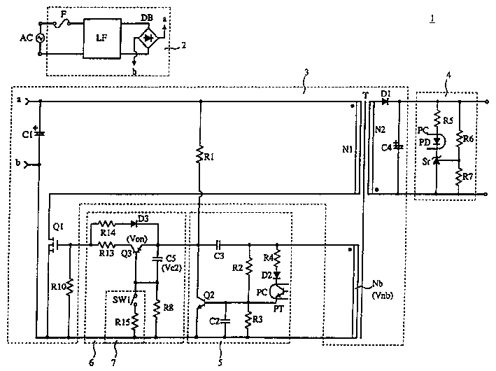
Fig. 8 is a kind of circuit diagram of RCC type Switching Power Supply of routine.As shown in this Fig, switching power unit 10 comprises an input circuit 2, DC-to-DC (DC-DC) converter circuit 3, voltage detector circuit 4 and control circuit 5.
Input circuit 2 comprises a fuse F, a filter circuit LF and a rectifier diode bridge circuit DB, and an AC power AC is connected to this input.In addition, an input of this input circuit 2 is connected to the end of filter circuit LF by fuse F, and another input of input circuit 2 is directly connected to the other end of the input side of filter circuit LF.In addition, the terminal on the outlet side of filter circuit LF is connected to each input of diode bridge DB.The output a of diode bridge DB and b are connected to the input a and the b of DC-DC converter circuit 3.
DC-DC converter circuit 3 comprises capacitor C1 and C4, transformer T, a main switch element and a diode D1, and this main switch element is MOS field-effect transistor (FET) Q1 and resistor R 1 and R10 for example.In addition, transformer T comprises a primary coil N1, a secondary coil N2 and the feedback coil Nb that polarity is identical with primary coil N1 that polarity is opposite with primary coil N1.Smmothing capacitor C1 is provided between the input a and b of DC-DC converter circuit 3, and primary coil N1 is in parallel with capacitor C1 with the series circuit of FET Q1.Therefore, the starting point of the primary coil N1 of transformer T is connected to the input a of DC-DC converter circuit 3, and the drain electrode of FET Q1 is connected to the end of primary coil N1, and the source electrode of FET Q1 is connected to the input of DC-DC converter circuit 3.In addition, the end of starting resistance R1 is connected to the starting point of primary coil N1, and the other end of resistor R 1 is connected to the grid of FET Q1.Resistor R 10 is connected between the grid and source electrode of FET Q1.In addition, the anode of rectifier diode D1 is connected to the end of the secondary coil N2 of transformer T, and smmothing capacitor C4 is connected between the starting point of the negative electrode of diode D1 and secondary coil N2.Diode D1 and capacitor C4 constitute a rectification and smoothing circuit.
Voltage detector circuit 4 is provided at the outside of DC-DC converter circuit 3, and comprise resistor R 5, R6 and R7, as LED P D and a shunt regulator Sr of the luminescent device of optical coupler PC.The capacitor C4 of the output of voltage detector circuit 4 and DC-DC converter circuit 3 is in parallel.In addition, the series circuit of the series circuit of resistor R 5, LED P D and shunt regulator Sr and resistor R 6 and R7 and capacitor C4 are in parallel.In addition, the negative electrode of LED P D is connected with the negative electrode of shunt regulator Sr.In addition, the reference edge of shunt regulator Sr is connected to the tie point between resistor R 6 and the R7.
Control circuit 5 comprises resistor R 2, R3, R4 and R13, capacitor C2 and C3, diode D2, as phototransistor PT and a NPN transistor Q2 of the light receiving element of optical coupler PC.Capacitor C3 and resistor R 13 are connected between the starting point of the grid of FET Q1 of DC-DC converter circuit 3 and feedback coil Nb.In addition, the collector and emitter of transistor Q2 is connected respectively to grid and the source electrode of FET Q1.In addition, the series circuit of resistor R 2 and resistor R 3 is connected between the starting point and end of feedback coil Nb.In addition, series circuit and the resistor R 2 of resistor R 4, diode D2 and the phototransistor PT in optical coupler PC are in parallel.In addition, the negative electrode of diode D2 is connected to the collector electrode of the phototransistor PT among the optical coupler PC.In addition, capacitor C2 is connected between the base stage and emitter of transistor Q2, and above-mentioned resistor R 3 is in parallel with capacitor C2.
The operation of the switching power unit 10 of formation as indicated above then, is described.At first, when power initiation, voltage is applied on the grid of FET Q1 by starting resistance R1, and the FETQ1 conducting.In this manner, power source voltage is applied to the primary coil N1 of transformer T, and produces the voltage that has with primary coil N1 identical polar in feedback coil Nb.Be provided to the grid of FETQ1 and the quick conducting of FET Q1 by resistor R 13 and capacitor C3 as this voltage signal of a positive feedback signal.At this moment, excitation energy is stored among the primary coil N1.
Because the electromotive force in feedback coil Nb makes charging current flow to capacitor C2 by resistor R 1.When the voltage of capacitor C2 surpasses the base stage of oxide-semiconductor control transistors Q2 and the forward drop between the emitter, transistor Q2 conducting.In this manner, the grid of FET Q1 and the vanishing basically of the voltage between the source electrode, thus FET Q1 is ended.
Therefore, the excitation energy that is stored in the turn-on cycle process of FET Q1 among the primary coil N1 of transformer T is released, pass through secondary coil N2 as electric energy, by the rectification of diode D1 institute, level and smooth by capacitor C4 institute, and be provided to the load (not illustrating in the drawings) of the output that connects voltage detector circuit 4.
When the electric charge in the capacitor C2 of charging by by resistor R 3 discharge circuits such as grade when discharge, charging voltage becomes the base stage that is equal to or less than transistor Q2 and the forward drop between the emitter, transistor Q2 ends.In addition, when the excitation energy among the primary coil N1 that is stored in transformer T is discharged by secondary coil N2 and is passed through the electric current vanishing of diode D1, in feedback coil Nb, produce a bounce voltage, wherein the starting point of coil is a positive polarity, and FET Q1 is by the conducting once more of this bounce voltage.When FET Q1 conducting, voltage is provided to the primary coil N1 of transformer T once more, and excitation energy is stored among the primary coil N1.
Therefore, above-mentioned vibration repeats in switching power unit 10.
Then, the feedback of being controlled by voltage detector circuit 4 is described.Under normal condition, detected at the output voltage of load-side voltage divider, and this detection voltage is compared with the reference voltage of shunt regulator Sr by resistor R 6 and R7.The variation of output voltage is amplified by shunt regulator Sr, and the electric current of the LED P D by optical coupler PC changes, and the light emission measure of LED P D also changes.In addition, according to the light quantity that the phototransistor PT by optical coupler PC is received, the impedance of phototransistor PT changes, and the charge constant of capacitor C2 correspondingly changes.Output voltage descends many more, and it is big more that above-mentioned charge constant then becomes, and output voltage more correspondingly descends, the FET Q1 that is caused by transistor Q2 is conducting to and forces time period of ending long more, that is to say that the conducting state time period of FET Q1 increases, force output voltage to increase.In addition, when output voltage increased, situation was opposite, and output voltage is forced to reduce.In this manner, realize voltage stabilizing control, make output voltage constant.
In addition, the situation that little load condition increases corresponding to above-mentioned output voltage, and the heavy load state is corresponding to the situation of above-mentioned output voltage decline.
In the RCC of the routine shown in Fig. 8 type switching power unit, the frequency of oscillation of known FET Q1 changes inversely with input power or power output basically.This that is to say frequency of oscillation (switching frequency) and the relation of exporting (bearing power) of illustrating shown in Fig. 5 (b).
Usually, when load diminishes, reduce for the switching loss of each switching manipulation, but as Fig. 5 (b) as shown in, power output is more little, i.e. load is more little, and then frequency of oscillation becomes high more, and the number of times of switching manipulation is big more, correspondingly switching loss increase.As a result, even load diminishes, the degree that reduces of switching loss is very little.Therefore, load is more little, and then the efficient of supply unit descends more.
In order to reduce the switching loss under this little load condition, can the design circuit constant, make frequency of oscillation become lower at the nominal load place, but when supply unit need be used for from the very for a short time wide region that loads to heavy load.That is, determined,, then caused problems such as transformer is saturated if frequency of oscillation is too low in the general main magnetic density of the frequency of oscillation of nominal load, the influence that exchanges pulsation, noise or the like by transformer.
In addition, when making the equipment of conventional RCC type switching power unit be in holding state, promptly be in above-mentioned little load condition, when frequency of oscillation uprises, because switching loss and in main switch element, produce heat.
For example, in the switching power unit that in printer, uses, when mains switch is in closed condition, can in the standby process, use a switching signal to make this power work at optimum working mode.On the other hand, in case the mains switch of printer is unlocked to print or the like operation, switching power unit turns back to the optimum working mode that is used for operate as normal.In addition, when the mains switch of printer is in opening,, then there is one period stand-by period if do not carry out printing.Because printer is little load in the stand-by period process, so as indicated abovely in the main switch element of the switching power unit that is used for this printer, produce heat.
For this problem, announce in 11-235036 number in Japanese unexamined patent, the present inventor discloses a kind of technology about switching power unit, wherein by at holding state input switch signal and the loss when reducing frequency of oscillation and improving standby.
In addition, in Japanese patent application 11-253550 number, the present inventor has proposed a kind of technology about switching power unit, the loss when wherein the frequency of oscillation in the rated range that uses when being reduced in standby continuously changes standby.
But, announce in the switching power unit in 11-235036 number being disclosed in Japanese unexamined patent, this supply unit is as a kind of RCC when switching signal is used for normal running.Therefore,, be not provided for reducing the measure of loss when supply unit is in holding state as in the above-mentioned printer, and the problem that causes input power to increase and in main switch element, generate heat in this existence.In addition, also have the intermittent oscillation operation, exporting ripple voltage in this case increases.In addition, in the switching power unit that proposes in Japanese patent application 11-253550 number, when this supply unit was in little load condition, frequency of oscillation reduced automatically.In this case, when frequency of oscillation reduces when too many, the response characteristic variation of load then, and correspondingly when with examine in Japanese unexamined patent please announce the technology described in 11-235036 number and compare the time, this frequency is limited to high frequency.Therefore, exist the effect that reduces the wastage and be worse than the imported problem of switching signal.
Detailed Description Of The Invention
First embodiment
With reference to the structure of Fig. 1 description according to the RCC type switching power unit of first embodiment of the invention.Fig. 1 is the circuit diagram that illustrates according to the switching power unit of first embodiment of the invention.In addition, in the described in the figure switching power unit 1, the switching power unit shown in Fig. 8 10 is added delay circuit 6 and delay switch circuit 7, and other circuit is with identical shown in Fig. 8.Therefore, give identical reference number, and omit concrete description identical part.
In the illustrated embodiment of Fig. 1, delay circuit in switching power unit 1 is provided between DC-DC converter circuit 3 and the control circuit 5, and comprises resistor R 8, R13 and R14, capacitor C5, diode D3 and as the PNP transistor Q3 of a switching device.In addition, resistor R 13 is transferred to delay circuit 6 by the control circuit from Fig. 85.In delay circuit 6, the series circuit of the series circuit of resistor R 13 and transistor Q3 and resistor R 14 and diode D3 is connected in parallel between the grid and the capacitor C3 in the control circuit 5 as the control end of FET Q1 in the DC-DC converter circuit 3.In addition, in above-mentioned delay circuit 6, an end of resistor R 13 is connected with the collector electrode of transistor Q3, and an end of resistor R 14 is connected with the anode of diode D3.In addition, capacitor C5 and resistor R 8 are in series, and are connected between the collector electrode and emitter of the transistor Q2 in the control circuit 5.Capacitor C5 and resistor R 8 constitute a time constant circuit.The base stage of transistor Q3 is connected to the tie point between capacitor C5 and the resistor R 8, and capacitor C5 is between the base stage and emitter of transistor Q3.
Delay switch circuit 7 is provided in the delay circuit 6, and comprises switch SW 1 and resistor R 15.Resistor R 8 in the series circuit of switch SW 1 and resistor R 15 and the delay circuit 6 is in parallel.Usually, switch SW 1 conducting.
Then, will the operation of the switching power unit that so constitutes be described.In addition, at this all major parts of operation are described.
At first, when voltage was provided to the grid of FET Q1 and FET Q1 conducting, supply voltage was provided to the primary coil N1 of transformer T, and produced and the identical voltage of primary coil N1 polarity in feedback coil Nb.This voltage signal is used as the grid that transistor Q3 and the resistor R 13 of a positive feedback signal by capacitor C3, conducting is provided to FET Q1, and the quick conducting of FET Q1.At this moment, excitation energy is stored among the primary coil N1.
Because the electromotive force of feedback coil Nb makes charging current also flow to capacitor C2 by resistor R 2.When the charging voltage of capacitor C2 surpasses the base stage of transistor Q2 and the forward drop between the emitter, transistor Q2 conducting.Therefore, the base stage of FET Q1 and the vanishing basically of the voltage between the source electrode, FET Q1 ends as a result.
Therefore, when FET Q1 conducting, being stored in excitation energy among the primary coil N1 of transformer T is used as electric energy and discharges, this electric energy is by secondary coil N2, by the rectification of diode D1 institute, level and smooth by capacitor C4 institute, and be provided to a load that is connected to the output of voltage detector circuit 4, it does not illustrate in the drawings.
When the electric charge in the capacitor C2 of charging by by comprising the discharge circuit discharge of resistor R 3, and the charging voltage of capacitor C2 is when becoming the base stage that is lower than transistor Q2 and the forward drop between the emitter, transistor Q2 ends.In addition, when the total excitation energy among the primary coil N1 that is stored in transformer T was discharged by secondary coil N2 and passes through the electric current vanishing of diode D1, the resilience voltage Vnb that capacitor C5 is produced in feedback coil Nb charged.
When the charging voltage Vc2 of capacitor C5 arrives the voltage Von of transistor Q3 conducting, transistor Q3 conducting, a voltage is applied to the grid of FET Q1, and FET Q1 conducting.
As indicated above, can postpone the conducting of FET Q1, the charging voltage Vc2 of the transistor Q2 in delay circuit 6 arrives voltage Von.In addition, the time period till the transistor Q3 conducting is determined by the time constant of the time constant circuit that comprises capacitor C5 and parallel resistor device R8 and resistor R 15.
When resistor R 15 was disconnected with resistor R 8, this time constant was determined by capacitor C5 and resistor R 8.In addition, be extended the time of delay that is used for FET Q1 conducting.In this manner, the conducting of FET Q1 is delayed, and the cut-off state time period of FET Q1 is extended.
In this manner, when little load, can keep substantially invariable frequency of oscillation, and, perhaps improve the pulsating voltage of output by avoiding the switching frequency increase to make that the efficient of RCC improves in the standby process because delay circuit 6 makes.In addition, the time of delay till by the conducting and the disconnection of the switch SW in delay switch circuit 71, in the time of can being adjusted to FET Q1 conducting, and can improve efficient when little load greatly.
Second embodiment
The structure of the RCC type switching power unit of second embodiment of the invention then, is described according to Fig. 2.Fig. 2 is the circuit diagram that illustrates according to the second embodiment of the invention switching power unit.In Fig. 2, the structure of the delay circuit 6 of the switching power unit 1a delay circuit 6 with the switching power unit 1 shown in Fig. 1 basically is identical.In addition, comprise switch SW 1 and resistor R 15 at the delay switch circuit 7a of switching power unit 1a.In the series circuit of switch SW 1 and resistor R 15, an end of resistor R 15 is connected to the grid of the FET Q1 in the DC-DC converter circuit 3, and an end of switch SW 1 is connected to the base stage of the transistor Q3 in the delay circuit 6.
The switching power unit 1a of Gou Chenging works according to the mode identical with switching power unit 1 in this manner.Correspondingly, can keep substantially invariable frequency of oscillation in little load, and by avoiding the increase of switching frequency, can improve the efficient of RCC when standby, perhaps can improve the pulsating voltage of output, simultaneously, by making switch SW 1 conducting and disconnecting the efficient improve widely when the little load.
In addition, in switching power unit 1a, because delay switch circuit 7a is provided at the position shown in Fig. 2, when resistor R 15 had little resistance, switching power unit 1a compares with switching power unit 1 had following effect.That is to say,, exist FET Q1 not to be switched on and switching power unit 1 situation that can not be activated correspondingly when under the state in switch SW 1 conducting of delay switch circuit 7 during starting switch supply unit 1.This be because, because the combined resistance of resistor R 8, R15 and R10 that the grid of FET Q1 and the voltage between the source electrode are connected by power supply is determined with the ratio between the resistance of resistor R 1, so can not be arrived threshold level at grid and the voltage between the source electrode of FET Q1.
On the other hand, in switching power unit 1a, because delay switch circuit 7a is in the position shown in Fig. 2, even therefore when switch SW 1 conducting during starting switch supply unit 1a, switching power unit 1a also can be activated.This be because, because the series circuit and the resistor R 8 of resistor R 15 and resistor R 10 are in parallel, and switch SW 1 conducting, even then resistor R 15 has the small resistor value, the negative effect that is not subjected to resistor R 15 at grid and the voltage between the source electrode of FET Q1.Correspondingly, even switch SW 1 conducting, the grid of FET Q1 and the voltage between the source electrode arrive threshold level, with conducting FET Q1.
The 3rd embodiment
Below, the structure of the RCC type switching power unit of third embodiment of the invention is described according to Fig. 3.Fig. 3 is the circuit diagram that illustrates according to the switching power unit of third embodiment of the invention.In the switching power unit 1b shown in Fig. 3, output power detector circuit 8 is connected delay switch circuit 7 and output power detector circuit 8 with one resistive element (impedance) is added in the switching power unit 1 shown in Fig. 1, and other circuit is identical to those shown in Fig. 1.Correspondingly, give identical reference number, and omit detailed description them to identical part.
In Fig. 3, the output power detector circuit 8 of switching power unit 1b is provided between the feedback coil Nb and control circuit 5 of DC-DC converter circuit 3, and this series circuit comprises as the diode D4 of rectifier cell and the capacitor C6 of the level and smooth element of conduct.Diode D4 and capacitor C6 are in series, and are provided between the two ends of feedback coil Nb.That is to say that the negative electrode of diode D4 is connected to the starting point of feedback coil Nb, and the end of capacitor C6 is connected to the end of feedback coil Nb.
In addition, in delay circuit 6, be connected to the tie point of capacitor C5 and resistor R 8, and the other end of resistor R 16 is connected to diode D4 in the output power detector circuit 8 and the tie point of capacitor C6 as the end of the R16 of resistive element.
Then, will the operation of the switching power unit 1b that so constitutes be described.The major part of switching power unit 1b is described at this in addition.
At first, a voltage is applied to the grid of FET Q1, and FET Q1 is switched on.Therefore, power source voltage is applied on the primary coil N1 of transformer T, and produces and the identical voltage of primary coil N1 polarity in feedback coil Nb.Be provided to the grid of FET Q1 and the quick conducting of FET Q1 by capacitor C3, transistor Q3 and resistor R 13 as the voltage signal of positive feedback signal.At this moment, excitation energy is stored among the primary coil N1.
Because the electromotive force in feedback coil Nb makes charging current flow to capacitor C2 by resistor R 2.When the charging voltage of capacitor C2 surpasses the base stage of oxide-semiconductor control transistors Q2 and the forward drop between the emitter, transistor Q2 conducting.Therefore, the vanishing basically of the voltage between FET Q1 grid and the source electrode, and FET Q1 ends.
When the cut-off state time of FET Q1 began, the capacitor C6 in output power detector circuit 8 was charged by the voltage that produces in the feedback coil Nb of transformer T.In addition, in the conducting state time period of FET Q1 process, the excitation energy that is stored among the primary coil N1 of transformer T is used as electric energy by secondary coil N2 discharge, by the rectification of diode D1 institute, level and smooth by capacitor C4 institute, and be provided to a load that connects the output of voltage detector circuit 4, not shown.
Then, the electric charge in the capacitor C2 of charging is by by comprising the discharge circuit discharge of resistor R 3 grades, and charging voltage is when becoming the base stage that is lower than transistor Q2 and the forward drop between the emitter, and transistor Q2 ends.In addition, the total excitation energy that is stored among the primary coil N1 of transformer T is discharged by secondary coil N2, and flow through the electric current vanishing of diode D1, the charging voltage Vc1 of capacitor C6 is released, by charging voltage Vc1 and the voltage Vnb that in feedback coil Nb, produces a voltage is applied to the emitter of transistor Q3, and the capacitor C5 in delay circuit 6 is recharged.When switch SW 1 conducting, the voltage of capacitor C5 increases according to the time constant of capacitor C5, parallel resistor device R8 and resistor R 15 and the resistor R 16 of connecting with capacitor C6.
Fig. 4 is the curve chart that the absolute value of the charging voltage Vc1 of the primary side that is illustrated in the switching power unit 1b shown in Fig. 3 capacitor C6 that constitutes output power detector circuit 8 changes.At this because the influence of leakage inductance of transformer T or the like, shown in the absolute value of charging voltage Vc1 and the load capacity of switching power unit 1b increase pro rata, as shown in Figure 4.
Therefore, when little load, the absolute value of the charging voltage Vc1 of capacitor C6 is less relatively, and it is elongated to arrive the required time of the voltage Von that makes transistor Q3 conducting up to the charging voltage Vc2 of the capacitor C5 that constitutes time constant circuit.Therefore, the conducting of FET Q1 is delayed, and the cut-off state time period of FET Q1 is extended result, the switching frequency reduction of FET Q1.On the other hand, when heavy load, the absolute value of the charging voltage Vc1 of capacitor C6 becomes relatively large, and up to the charging voltage Vc2 of capacitor C5 arrival is shortened the required time of voltage Von of transistor Q3 conducting.Therefore, the conducting of FET Q1 is accelerated, and the cut-off state time period of FET Q1 is shortened.
Because the capacitor C6 as voltage source is placed in the path of capacitor C5 and resistor R 16, so the absolute value of the voltage of capacitor C6 is big more, then the voltage increase of capacitor C15 is fast more.
When the charging voltage Vc2 of capacitor C5 arrives voltage Von, transistor Q3 conducting, voltage is applied on the grid of FET Q1, and FET Q1 conducting.
In this manner, can postpone the conducting of FET Q1, when the charging voltage Vc2 of the transistor Q2 in delay circuit 6 arrives voltage Von till.
When making that by the switch SW in the off delay switching circuit 71 resistor R 15 disconnects with resistor R 8, time constant is determined by capacitor C5 and resistor R 8.Correspondingly, be extended the time of delay till when FET Q1 conducting.Therefore, the conducting of FET Q1 is delayed, and the cut-off state time period of FET Q1 is extended.
At this, the result who increases as the load capacity of switching power unit 1b causes the change of switching frequency shown in Figure 5.Fig. 5 is the curve chart that is illustrated in the change of switching frequency in switching power unit of the present invention and the ordinary tap supply unit.In Fig. 5, (a) and (a) ' change of the switching frequency of switching power unit 1b is shown, and the change of the switching frequency of conventional switching power unit 10 (b) is shown.When little load, the frequency of switching power unit of the present invention (a) is compared low especially with the frequency (b) of the switching power unit 10 of routine, and when the load increase surpassed specific POL, frequency (a) changed with frequency (b) same way as with routine.In addition, when switch SW 1 disconnected, this frequency was by curve (a) ' illustrate.
The 4th embodiment
The RCC type switching power unit of fourth embodiment of the invention is described according to Fig. 6 below.Fig. 6 is the circuit diagram that illustrates according to the switching power unit of fourth embodiment of the invention.In Fig. 6, the structure of the delay circuit 6 of the switching power unit 1c delay circuit 6 with the switching power unit 1 shown in Fig. 1 basically is identical.In addition, the delay switch circuit 7b of switching power unit 1c comprises resistor R 15 and as the phototransistor PT2 of the part of optical coupler PC2.The series circuit of resistor R 15 and phototransistor PT2 and resistor R 8 are in parallel.That is to say that an end of resistor R 15 is connected to the capacitor C5 in the delay circuit 6 and the tie point of resistor R 8, and the emitter of phototransistor PT2 is connected to the source electrode of the FETQ1 in the DC-DC converter circuit 3.
In addition, an external remote control signal REM is provided to the anode of the light-emitting diode among the optical coupler PC2, the negative electrode of LED P D2 is by resistor R 17 ground connection.
So the switching power unit 1c that constitutes works according to the mode identical with switching power unit 1.That is to say that when external remote control signal REM was high level signal, LED P D2 was luminous, and as the phototransistor PT2 conducting of light-receiving source part.Therefore, resistor R 15 is in parallel with resistor R 8, and the time constant of the time constant circuit that is made of capacitor C5 and resistor R 8 changes.Correspondingly, when switching power unit 1c is used for above-mentioned printer, can be by remote signal be switched to high level signal and standby mode is changed into normal mode of operation.
The 5th embodiment
The RCC type switching power unit of fifth embodiment of the invention then, is described according to Fig. 7.Fig. 7 is the circuit diagram that illustrates according to the switching power unit of fifth embodiment of the invention.In the switching power unit 1d shown in Fig. 7, resistor R 16 is provided between the end of resistor R 6 of voltage detector circuit 4 of the switching power unit 1 shown in output and Fig. 1, and is provided for detecting the current detection circuit 9 of the electric current of resistor R 16.In addition, provide phototransistor PT2, to replace the switch SW 1 in the delay switch circuit 7 as the light receiving element of the optical coupler PC2 in the current detection circuit 9.Current detection circuit 9 comprises resistor R 16 to R23, capacitor C11, comparator C OMP1 and COMP2, and reference voltage Vref.Resistor R 16 is connected between the end of the output of voltage detector circuit 4 and resistor R 6.Resistors in series R17 and resistor R 18 between the output of voltage detector circuit 4.The positive input terminal of comparator C OMP1 is connected to the tie point of resistor R 17 and resistor R 18.Be connected by the parallel circuits that series circuit constituted of the LED P D2 of the series circuit of series circuit, resistor R 21 and the capacitor C11 of resistor R 19 and resistor R 20 and resistor R 22 and optical coupler PC2 between the starting point of secondary coil N2 of the tie point of resistor R 16 and resistor R 6 and transformer T.In addition, an end of resistor R 22 is connected with the anode of LED P D2.In addition, the negative input end of comparator C OMP1 is connected to the tie point of resistor R 19 and resistor R 20.In addition, an end of the negative input end of the output of comparator C OMP1, comparator C OMP2 and resistor R 23 is connected to the tie point of resistor R 21 and capacitor C11.In addition, the other end of the output of comparator C OMP2 and resistor R 23 is connected to the tie point of resistor R 22 and LED P D2.Reference voltage Vref is connected to the positive input terminal of comparator C OMP2.
In addition, the delay switch circuit 7c in switching power unit 1d is identical with delay switch circuit 7b structure among the switching power unit 1c shown in Fig. 5, and comprises the phototransistor PT2 of resistor R 15 and optical coupler PC2.The series circuit of resistor R 15 and phototransistor PT2 and resistor R 8 are in parallel.That is to say that an end of resistor R 15 is connected to the capacitor C5 in the delay circuit 6 and the tie point of resistor R 8, and the repellel of phototransistor PT2 is connected to the source electrode of the FET Q1 in the DC-DC converter circuit 3.
The operation of the switching power unit 1d of formation as indicated above then, is described.The major part of switching power unit 1d is described at this in addition.
When the load of switching power unit 1d becomes standby load (little load) from nominal load (heavy load), and output current is when reducing, and the output of the comparator C OMP1 in current detection circuit 9 becomes open-circuit condition.
At this moment, in current detection circuit 9, when the voltage of the capacitor C1 in the RC time constant circuit to rise by the needed speed of time constant and when surpassing reference voltage Vref, the output of comparator C OMP2 becomes low level signal.Then, the electric current in LED P D2 stops to flow, and LED P D2 extinguishes, and ends as the phototransistor PT2 of light receiving element.Therefore, time constant becomes and is not subjected to the influence of resistor R 15, and comprises that the time constant of the time constant circuit of capacitor C5 and resistor R 8 changes.Therefore, when switching power unit 1d was used for above-mentioned printer, because the output signal of comparator C OMP2 becomes a low level signal, so normal manipulation mode became standby mode.
When a current detection circuit is provided in the above-mentioned switching power unit, can obtain an effect, even when wherein nominal load becomes standby load, operator scheme is constant in the determined time period by time constant.
Then, when waiting for that load becomes nominal load, the output step-down of the comparator C OMP1 in current detection circuit 9.Be less than or equal to reference voltage Vref when the voltage of the capacitor C11 in the RC time constant circuit reduces and becomes, the output of comparator C OMP2 becomes a high level signal, and standby mode becomes the normal rating operator scheme.
When a current detection circuit is provided in the switching power unit, occurs becoming the moment pattern of nominal load, and under any load condition, can realize optimal operator scheme from the wait load.
As indicated above, in the fifth embodiment of the present invention, can change pattern automatically by using current detection circuit to detect the electric current of output loading.In addition, when a timer circuit is provided, can handle any unexpected load variations.
For example, in printer, owing to printing, paper feed, printer control or the like make load change fast.When the conventional efficient power device that is in holding state that uses automatic change pattern in this state, carry out switching between standby mode and the normal mode of operation according to the load frequent on printer ground, and the switching power unit that correspondingly, needs printer has good response.Therefore, because this response has priority, can not dynamically reduce switching frequency.
On the contrary, when switching power unit of the present invention is used for inductor, because even printer is in the wait load condition, in certain period of time, normal mode of operation does not become standby mode yet, correspondingly, and when load frequent with when changing apace, printer is operated in normal mode of operation, and result's switching power unit of the present invention is reliable.In addition, standby mode switches to normal mode of operation immediately, and because processing before printing or the like makes that the load when switching is less relatively usually, and no problem aspect response.
In addition, in each embodiment of the present invention, the phototransistor of this switch and the optical coupler in the time of delay commutation circuit is used as the two-state device under the state that is operated in two states and illustrates, but the invention is not restricted to this.By constituting a delay switch circuit, wherein use the device that is operated in the plural state in conjunction with switch, phototransistor or the like in optical coupler.In this case, can carry out meticulous adjusting according to switching frequency.
According to the present invention, forbid main switch element conducting in special time by delay circuit, and the cut-off state cycle of vibration is extended, make by using switching circuit to change time of delay according to two or more classifications, and correspondingly, when comparing with the situation of not using delay circuit, can reduce the switching frequency of main switch element, and by using switching circuit to be arranged on required frequency to the switching frequency of main switch element.Therefore, the frequency of oscillation increase under little load and holding state is suppressed, and standby power is suppressed, and the heating in main switch is suppressed, and perhaps can suppress by being interrupted the output ripple voltage that vibration is caused.
In addition, owing to the delay circuit that comprises switching device and time constant circuit between the control end of feedback coil that is provided at transformer and main switch element, and the switching circuit that is provided for the time constant of constant circuit switching time, therefore the ON time of switching device changes according to the time constant of time constant circuit, also can change the time constant of time constant circuit, and can when little load, raise the efficiency greatly by switching circuit.
In addition, owing to provide and prolong output power detector circuit and time of delay circuit, wherein in the output power detector circuit, the voltage of the feedback coil of transformer is level and smooth by rectifier cell institute's rectification and smoothed element institute, and should prolong circuit time of delay as the resistive element between the control end that is connected to delay circuit by the output power detector circuit, therefore further postpone the conducting of main switch element, and can reduce the switching frequency of main switch element, the result can reduce frequency of oscillation in little load, and the efficient of the RCC can improve standby time the and improve output ripple voltage.
In addition, because switching circuit can be switched by external signal, therefore can easily change the switching frequency of main switch element from the outside.
In addition, owing to be provided for detecting current detection circuit by the electric current of secondary coil, and provide other switching circuit, be used for when current detection circuit detects load current or bearing power under holding state after certain period of time, therefore the time of delay of switching delay circuit, can automatically change the switching frequency of main switch element.
Although describe the present invention according to certain embodiments, the professional in this area can adopt many other conspicuous change and variations.Therefore, the present invention can't help this concrete open the restriction, and is only limited by appended claims.