CN1199218C - Method for creating field electron emission material and field electron emitter comprising said material - Google Patents
Method for creating field electron emission material and field electron emitter comprising said material Download PDFInfo
- Publication number
- CN1199218C CN1199218C CNB008099960A CN00809996A CN1199218C CN 1199218 C CN1199218 C CN 1199218C CN B008099960 A CNB008099960 A CN B008099960A CN 00809996 A CN00809996 A CN 00809996A CN 1199218 C CN1199218 C CN 1199218C
- Authority
- CN
- China
- Prior art keywords
- mixture
- electronic emission
- silica
- precursor
- amorphous silica
- Prior art date
- Legal status (The legal status is an assumption and is not a legal conclusion. Google has not performed a legal analysis and makes no representation as to the accuracy of the status listed.)
- Expired - Fee Related
Links
Images


Classifications
-
- H—ELECTRICITY
- H01—ELECTRIC ELEMENTS
- H01J—ELECTRIC DISCHARGE TUBES OR DISCHARGE LAMPS
- H01J1/00—Details of electrodes, of magnetic control means, of screens, or of the mounting or spacing thereof, common to two or more basic types of discharge tubes or lamps
- H01J1/02—Main electrodes
- H01J1/30—Cold cathodes, e.g. field-emissive cathode
- H01J1/304—Field-emissive cathodes
-
- H—ELECTRICITY
- H01—ELECTRIC ELEMENTS
- H01J—ELECTRIC DISCHARGE TUBES OR DISCHARGE LAMPS
- H01J9/00—Apparatus or processes specially adapted for the manufacture, installation, removal, maintenance of electric discharge tubes, discharge lamps, or parts thereof; Recovery of material from discharge tubes or lamps
- H01J9/02—Manufacture of electrodes or electrode systems
- H01J9/022—Manufacture of electrodes or electrode systems of cold cathodes
- H01J9/025—Manufacture of electrodes or electrode systems of cold cathodes of field emission cathodes
-
- C—CHEMISTRY; METALLURGY
- C01—INORGANIC CHEMISTRY
- C01B—NON-METALLIC ELEMENTS; COMPOUNDS THEREOF; METALLOIDS OR COMPOUNDS THEREOF NOT COVERED BY SUBCLASS C01C
- C01B32/00—Carbon; Compounds thereof
- C01B32/05—Preparation or purification of carbon not covered by groups C01B32/15, C01B32/20, C01B32/25, C01B32/30
-
- H—ELECTRICITY
- H01—ELECTRIC ELEMENTS
- H01J—ELECTRIC DISCHARGE TUBES OR DISCHARGE LAMPS
- H01J1/00—Details of electrodes, of magnetic control means, of screens, or of the mounting or spacing thereof, common to two or more basic types of discharge tubes or lamps
- H01J1/02—Main electrodes
- H01J1/30—Cold cathodes, e.g. field-emissive cathode
- H01J1/304—Field-emissive cathodes
- H01J1/3048—Distributed particle emitters
-
- H—ELECTRICITY
- H01—ELECTRIC ELEMENTS
- H01J—ELECTRIC DISCHARGE TUBES OR DISCHARGE LAMPS
- H01J63/00—Cathode-ray or electron-stream lamps
- H01J63/02—Details, e.g. electrode, gas filling, shape of vessel
-
- H—ELECTRICITY
- H01—ELECTRIC ELEMENTS
- H01J—ELECTRIC DISCHARGE TUBES OR DISCHARGE LAMPS
- H01J9/00—Apparatus or processes specially adapted for the manufacture, installation, removal, maintenance of electric discharge tubes, discharge lamps, or parts thereof; Recovery of material from discharge tubes or lamps
- H01J9/02—Manufacture of electrodes or electrode systems
-
- B—PERFORMING OPERATIONS; TRANSPORTING
- B82—NANOTECHNOLOGY
- B82Y—SPECIFIC USES OR APPLICATIONS OF NANOSTRUCTURES; MEASUREMENT OR ANALYSIS OF NANOSTRUCTURES; MANUFACTURE OR TREATMENT OF NANOSTRUCTURES
- B82Y40/00—Manufacture or treatment of nanostructures
Landscapes
- Engineering & Computer Science (AREA)
- Manufacturing & Machinery (AREA)
- Chemical & Material Sciences (AREA)
- Organic Chemistry (AREA)
- Inorganic Chemistry (AREA)
- Cathode-Ray Tubes And Fluorescent Screens For Display (AREA)
- Cold Cathode And The Manufacture (AREA)
- Electrodes For Cathode-Ray Tubes (AREA)
Abstract
A field electron emission material is created by applying a silica precursor to graphite particles (11); processing the silica precursor to produce amorphous silica (12) which is doped and/or is heavily defective, and disposing the graphite particles (11) upon an electrically conductive surface (14) of a substrate (13) such that they are at least partially coated with the amorphous silica (12).
Description
Technical field
The present invention relates to a field electronic emission body and an electronic emission equipment that an electronic radiating material forms this class material of methods and applications.
Background technology
In classical electronic emission, the high electric field of material surface is as near 3 * 10
9Vm
-1, the thickness of surface-potential barrier can be reduced to electronic energy leaves this material by the quantum mechanical tunnel effect degree.Utilize the sharp point of atom to concentrate macroscopical electric field can realize these necessary conditions.Use low work function surface energy and further increase an electronic emission electric current.Well-known Fowler-Nordheim equation has been described measuring of an electronic emission.
Original technology that a kind of important relevant radiation body based on the tip is arranged has been described the electronic emission body and the radiation array of the field electronic emission of using sharp point (tip).Those skilled in the art's main purpose is hole (gate circuit) to be placed away from each single radiation most advanced and sophisticated less than the electrode of 1 μ m, applies 100 volts or lower current potential and can realize required high electric field one these radiate bodies and are called the gate array.The C.A.Spindt that works in California Stanford Research Institute has described this gate array of realizing first (J.Appl.Phys.39,7, pp3504-3505, (1968)).The array of Spindt has used molybdenum radiation most advanced and sophisticated, and its method for making is to use from macking technique by vacuum evaporation evaporation of metal SiO to the silicon substrate
2The cylindricality recess of layer.
At the seventies, make the another kind of method of homogeneous structure and use directional solidification eutectic alloy (DSE).It is the metallographic that fiber is aimed in another phase matrix that the DSE alloy has a kind of form.It is outstanding that matrix can stay fiber through dark etching.After the etching, vacuum evaporation insulating barrier and conductive layer can be made into door again.The evaporating materials that is deposited on the tip is used as mask, stays annular space around outstanding fiber.
A kind of important method is to utilize the silicon microfabrication to form the gate array, has made an electronic emission display with this technology at present, receives the concern of the many tissues in the whole world.
All are based on the radiology system at tip, and the subject matter of existence is the damage that is easy to suffer ion bombardment, large-current electric resistance heating, and disastrous damage is that electrical breakdown causes in the device.The making large-area devices is both difficult and expensive.
Greatly about 1985, once found can be on by the substrate of hydrogen-methane atmosphere heating growing diamond membrane, make large tracts of land field emission body, promptly need not the field emission body at precision machined tip.
Utilization was hanged down and is reached 3MVm according to people such as Wang report (Electron, Lett., 27, pp1459-1461 (1991)) in 1991
-1Electric field, can obtain an electronic emission electric current from large-area diamond film.Some people thinks that this performance is the faceted low electron affinity of diamond (the 111) (Xu that combines with the local high density of graphite fusion at random, Latham and Tzeng:Electron.Lett., 29, pp1596-159 (1993) is although also have some other explanation.
Use laser ablation (ablation) and ion beam technology, now can be on substrate with the grow coating of high diamond content of room temperature.Yet the visual plant of application of expensive is all wanted in all these class processing, can not predict the performance of the material of making like this.
A kind of the electronic emission display (FED) that U.S. S.I.Diamon describes is used as electron source to a kind of material that calls AmorphicDiamond (amorphous diamond).The University of Texas has permitted the coated with CVD (chemical vapor deposition) diamond technology.This material is by making the graphite laser ablation to substrate.
Since the sixties, another group researcher studying always with electrode between in a vacuum the relevant mechanism of electrical breakdown.(Latham and Xu, Vacuum, 42,18, pp1173-1181 (1991)) as everyone knows along with the voltage between the electrode increases, just has electric current to flow up to reaching a certain critical value, and have a noisy little electric current to begin to flow this moment.This electric current along with electric field be dull, progressively increase, up to reaching another critical value, then can cause electric arc.It is generally acknowledged that the key of improving voltage cut-off is to eliminate these prebreakdown current sources.Think that now active site is metal-insulator-vacuum (MIV) structure, this structure is formed by embedding insulating particles or conductive patch on the insulation fragments such as oxidation on metal surface thing.In these two kinds of occasions, electric current all is derived from hot-electron processes, and this process has been quickened electronics, causes producing on surface-potential barrier standard-thermionic emission.The existing description of this situation (as Latham, High Voltage Vacuum Insulation, Academic press (1995)) in scientific literature.Though existing some technology (as particle accelerator) have been adopted this research contents and improved the vacuum insulation degree, still this knowledge of few people's research and utilization is formulated an electronic emission body up to date.
Latham and Mousa (J.Phys.D:Appl, phys.19, pp699-713 (1986)) the synthetic metal-insulator tip-based radiation body of using above-mentioned hot-electron processes has been described, in 1988, S.Bajic and R.V.Latham (Journal of physics D Applied Physics, vol.21 200-204 (1988)) describes a kind of synthetic and formulated high-density metal-insulator-metal-insulator-vacuum (MIMIV) radiation position, the conducting particles of this synthetic is dispersed in the epoxy resin, and coating is coated onto the surface with the standard spin-on technology.
Afterwards in nineteen ninety-five, Tuck, Taylor and Latham (GB2304989) replace epoxy resin and have improved above-mentioned MIMIV radiation body with inorganic insulator, have both improved stability, can work in the shutoff vacuum plant again again.
Tuck, Taylor and Latham (GB2304989) propose, and the MIMIV radiation is the general characteristic that contains the conducting particles inorganic insulation layer.This to a certain degree is being correct, but still strong request identification obtains the particle of the required electric field of radiation and the combination of insulating material, can obtain the radioactive department bit density like this, and the use that whole evenly performance is generally electronic installation is accepted.
Summary of the invention
All preferred embodiments of the present invention provide the combination of particle and insulating material, and the field electronic emission has been proposed the good unusually structural form of characteristic.
According to an aspect of the present invention, propose a kind of method that forms an electronic radiating material, comprised step:
Graphite particle is added silica precursor (precursor);
Handle described silica precursor, form through mixing and/or the amorphous silica of major defect being arranged; With
Described graphite particle is placed substrate conductive surfaces, make them be coated with described amorphous silica to small part.
In this manual, the term " major defect " that is applied to silicon dioxide is illustrated in the silicon dioxide, and band edge (band edges) is with the various states diffusion, and these states can or needn't be restricted, make them extend to band gap, be beneficial to carry charge carrier with hopping reaction mechanism.
Described graphite particle can be formed granular projection or the tip that is produced on the described conductive surface, perhaps described graphite particle is a loose particles.
Said method can comprise step:
Described graphite particle and described silica precursor are mixed into first mixture;
Described first mixture is applied to described conductive surface; Then
Handle described first mixture and form second mixture that described graphite particle is mixed with described amorphous silica.
In addition, these class methods can comprise step:
Described graphite particle and described silica precursor are mixed into first mixture;
Handle described first mixture, form second mixture that described graphite particle is mixed with described amorphous silica; Then
Described second mixture is applied to the described conductive surface of described substrate.
Described silica precursor, all available spin coating of first or second mixture, spraying or typography are applied to described conductive surface.
The major advantage of this class spin coating, printing, spray bar or similar technology is to avoid using relatively costly plasma or vacuum covering technology.
Described typography can be ink-jet printing process or silk-screen printing technique.
Described silica precursor, first or second mixture can be coated onto the selected position of described conductive surface with emission (lift-off) technology.
Described silica precursor, described first or second mixture are the liquid ink form.
Printing ink is represented a kind of liquid that contains described silica precursor or amorphous silica, described first or the situation of second mixture under, described graphite particle is a suspension.
Described silica precursor can be the sol-gel form.
Described sol-gel can be synthetic with tetraethyl orthosilicate.
Described sol-gel can comprise in propan-2-ol (propan-2-ol) solvent and contain silicon dioxide, adds or do not add acetone.
Described silica precursor can be a soluble precursors.
Described soluble precursors can be the soluble polymer precursor.
Described soluble polymer precursor comprises silicon Bei Ban oxane (silsequioxane) polymer.
Described silsequioxane polymer comprises β-chloroethyl silicon Bei Ban oxane (β-chloroethyl-silsequioxane) in solvent.
Described silica precursor can comprise the silica colloidal dispersion.
Described silica precursor, described first or second mixture are the dry color form.
Colorant is represented: containing the dry mash of described silica precursor or amorphous silica, in the described first or second mixture occasion, is described graphite particle; Or in the described first or second mixture occasion, graphite particle precoating has described silica precursor or amorphous silica, as our patent GB2304989 is described.
Described amorphous silica or its precursor can be mixed with metallic compound or metal cation.
Described metallic compound can be a nitrate.
Described metallic compound can be an organo-metallic compound.
Described amorphous silica can mix with tin oxide or tin indium oxide.
Described amorphous silica available iron and/or manganese compound doped.
The described processing of described amorphous silica can comprise heating.
Described heating is implemented with laser.
The described processing of described amorphous silica can comprise exposure.
Described exposure can be undertaken by predetermined pattern.
Described graphite particle can comprise carbon nano-tube (nanotubes).
Described graphite particle can comprise the non-graphite particle that applies or catch graphite.
Described graphite can be oriented and be exposed to prism planes.
When handling described amorphous silica, each described particle can have the described amorphous silica of one deck, and described amorphous silica layer is in the primary importance between described conductive surface and the described particle and/or the second place between described particle and park electronic radiating material environment, thus at least some described first and/or the second place form the electronic emission position.
The present invention extends to the field electronic emission body that contains an electronic radiating material, and the method for described electronic radiating material utilization either side of the present invention forms.
According to a further aspect in the invention, provide a kind of method of electronic emission equipment that forms, may further comprise the steps:
Form an electronic emission body according to the described method that forms an electronic radiating material of claim 1;
For being equipped with, described electronic emission body make it bear electric field so that the device of its emitting electrons.
In the said method, described electronic emission equipment comprises the control electrode of the array of apertures of aiming at the substrate and the band of described the little chip arrays of electronic emission body, and described electrode is supported in radiation body small pieces top with insulating barrier.
In the said method, described hole is the flute profile formula.
In the said method, described electronic emission equipment is as plasma reactor, corona discharge assembly, static discharge device, ozone generator, electron source, electron gun, electronic installation, x ray tube, vacuum gauge, aerating device or ion propeller.
In the said method, described field electronic emission body provides total current for the operation of described electronic emission equipment.
In the said method, described electronic emission body provides startup, triggers or causes electric current to described electronic emission equipment.
In the said method, described electronic emission equipment comprises display unit.
In the said method, described electronic emission equipment comprises lamp.
In the said method, described lamp is essentially the plane.
In the said method, described electronic emission body is connected to electric driver through ballast resistor, with the restriction electric current.
In the said method, a ballast resistor places below each described radiation body small pieces as resistor disc.
In the said method, the material of described radiation body and/or fluorescent material are coated on one or more one-dimensional electric orbit arrays, and described conductive traces is positioned to by the electronic driver addressing, to form the scanning illuminating line.
In the said method, described electronic emission body places gaseous state, liquid state, solid-state or vacuum environment.
In the said method, described electronic emission equipment comprises the negative electrode of the translucent and relative anode arrangement of an optics, the electronic impact anode of cathode emission and cause the anode electroluminescence, and this electroluminescence can be seen by the optics semitransparent cathode.
Obviously, electrical terms " conduction " is relative with " insulation ", depends on their Fundamentals of Measurement.Semiconductor has useful conductive characteristic, in fact can be used as conducting particles in the present invention.In this manual, the conductance of each described conducting particles is 10 of insulating material at least
2Doubly (preferably be at least 10
3Or 10
4Doubly).
The present invention has many different embodiment, and n example is described below.Obviously, in fact the feature of embodiment or example can be used in combination the feature of other embodiment or example.
Description of drawings
Brightly there are a plurality of similar embodiment effective in order to understand the present invention better and to show, can be with reference to all accompanying drawings, wherein
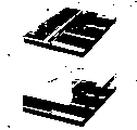
Fig. 1 illustrates a kind of MIMIV field emission body material;
Fig. 2 a and 2b illustrate the voltage-current characteristic of two kinds of different negative electrodes;
Fig. 3 a and 3b illustrate the radiation image of Fig. 2 a and 2b negative electrode respectively and make comparisons;
Fig. 4 illustrates the radiation image of a negative electrode; With
Fig. 5 a~5c illustrates the field emission device that each example is used the material of this paper announcement.
Embodiment
Fig. 1 illustrates a kind of MIMIV radiation body material of Tuck, Taylor and Latham (GB2304989) description, in the inorganic electric insulation matrix 12 on conductive substrates 13 conducting particles 11 is arranged.Dielectric substrate 13 adds one deck conductive layer 14 earlier before coating, add conductive electrode 14 and can utilize the whole bag of tricks, includes but not limited to vacuum and plasma coating, plating, electrodeless plating and printing ink based method.
Though all embodiment of the present invention are not limited to the particular transmitter reason, the radiative process of material shown in Figure 1 it is believed that as follows.Originally, insulator 12 forms a kind of obstruct and contacts between particle 11 and substrate, and particle voltage will be elevated to the highest equipotential current potential that it can be surveyed, and this is called antenna effect.When applying voltage, this current potential height must be enough to form an electrical forming conducting channel 17 between particle and substrate a certain.Then, the particle current potential promptly to the current potential reversing of substrate 13 or conductive layer 14, generally is positioned to the negative electrode track.So the residual charge of particle top forms a high electric field, causes second electrical forming raceway groove 18 and relevant metal-insulator-vacuum (MIV) thermionic emission position.After this connection process, can draw reversible field emission electric current 20 from this position.
Connect the required lasting electric field of electrical forming raceway groove by the ratio decision of particle height 16 with the interior stromal thickness in conducting channel 15 zones.For the minimal turn-on electric field, the thickness of conducting channel matrix 12 should be significantly less than the particle height.The granularity of conducting particles is generally (but being not limited to) 0.1~400 micron, preferably is narrow size distribution.
" raceway groove ", " conducting channel " or " electrical forming raceway groove " refer to a certain zone of insulator, and its characteristic was generally made local correction with the forming technology that certain relates to electric charge injection or heating.This correction helps electronics from conducting electricity back contact injection insulator, makes electronics move the acquisition energy by insulator, and injects vacuum by surface-potential barrier.In crystalline solid, can directly inject conduction band, or in amorphous materials, inject to be in and to make the energy level that electronics jumps and conducts.
Now be surprised to find, control the variant of amorphous silica meticulously, can provide a kind of desirable material the insulator composition of MIMIV structure.Different with many candidates' amorphous materials, amorphous silica has (can localize or not the tail state of local branch) of a diffusion but the strict band gap that limits, thereby can revise its characteristic with similar semiconductor processing technology (as mixing),, donor level gives the n type characteristic of this material expectation so that being provided.In the application GB2340299 that we await the reply jointly, described the effect of this donor level, the reader has been done guidance.Should be understood that as all amorphous materialses, produce the required concentration of dopant of electronic effect and be higher than crystalline material far away.In some cases, because structure has been introduced high concentration impurities, the alloying of material can appear also.Except adding alloy, provide alms giver and internal electric field centrostigma by form with lattice defect and granule boundary controlling diaphragm, can revise the electrology characteristic of silicon dioxide.Find that perfect high-quality silicon dioxide film does not provide essential charge carrier/conduction state on the electricity.Find also that in addition the prescription of unoptimizable or incorrect processing causes too perfectly silicon dioxide too easily.
Silicon dioxide (SiO
2) be a kind of polymorphic structure of complexity, form by the silicon atom and the oxygen atom of tetrahedral structure, wherein, tetrahedron is in the combination by bridge joint oxygen key of each corner.Zero defect silicon dioxide must mean pure and perfect crystalline material, the band edge anury attitude that it is sharp-pointed.
For silicon is done thermal oxidation and the almost flawless amorphous silica film of growing, semicon industry has been done very big effort, the electron pole silicon dioxide that makes thus can be used as the gate circuit medium of metal oxide semiconductor device, and the defect concentration of these media is very low, high pressure resistant puncture.
On the other hand, the silicon dioxide by method deposits such as plasma, sol-gel or polymer precursors is amorphous, and is chaotic on component, structure or form.For example, than the silicon dioxide of heat growth, it contains the much higher point defect of density, as dangling bonds, non-bridge joint oxygen key and hydrogen terminating key, makes the material non-stoichiometry.Except other factors, the electrology characteristic of this class film depends on that deposit, impurity add and follow-up annealing.The available traditional burner, rapid thermal annealing of annealing or use laser to realize.
Therefore, by controlling deposition technology and avoiding prolonging after annealing (post-annealing), can controllably be formed with the silicon dioxide of major defect.This class material can be described as and has many electronic states that can localize or can not localize, and makes them extend to band gap, causes wired mao wide band edge (often being called magnetic tape trailer) thus, and reduces full band gap.
The conditional electronic industry of good dielectric film of attempting to grow is avoided this class major defect silicon dioxide always, and main cause is that its anti-electrical breakdown is poor.This characteristic results from various charged attitudes and middle condition, for example provides conductive path by material by jump conduction (hopping conduction) and ionization process of electronics.
Silicon dioxide film with correct characteristic can be used the sol-gel manufactured, and the follow-up heat treatment of suspension formulation, coating process and layer plays key effect to final radiation body performance.
The exemplary process that forms this class sol-gel is as follows.
Example 1
Tetraethyl orthosilicate (10ml) and MOS grade propan-2-ol (47ml) are mixed and are cooled to 5~10 ℃ with 1000r.p.m, then this mixture is added the solution that contains cone nitric acid (0.10g) in the deionized water (2.5g), after spending 2 hours this mixture is transferred to airtight container, in refrigerating chamber with 4 ℃ of storages, up to use.
Example 2
Tetraethyl orthosilicate (10ml) and acetone (13ml) and MOS grade propan-2-ol (34ml) are mixed and are cooled to 5~10 ℃ with 1000r.p.m, then this mixture is added the solution that contains concentrating hydrochloric acid (0.25g) in the deionized water (2.5g), after spending 2 hours this mixture is transferred to airtight container, in refrigerating chamber with 4 ℃ of storages, up to use.
Example 3
Tetraethyl orthosilicate (10ml) and acetone (13ml) and MOS grade propan-2-ol (34ml) are mixed and are cooled to 5~10 ℃ with 1000r.p.m, then this mixture is added the solution that contains cone nitric acid (0.10g) in the deionized water (2.5g), after spending 2 hours this mixture is transferred to airtight container, in refrigerating chamber with 4 ℃ of storages, up to use.
Add for example tin oxide, can advantageously revise the band gap of silicon dioxide.SnO
2Be similar to SiO
2The band gap of silicon dioxide is~9eV, and SnO
2Band gap be~3.6eV that these two kinds of mixtures of material have the band gap between the two.In addition, SnO
2Because easy anoxic is so be a kind of n section bar material.Therefore, SiO
2With SnO
2Suitable mixture had both had the band gap narrower than simple silicon dioxide, had n type characteristic again.Tin indium oxide or antimony tin also can be used as additive.
The other method that can revise the silicon dioxide characteristic electron is that the amorphous silica net is added the metallicity cationic form.We find, can reduce the mixture of iron and manganese salt (as nitrate) adding sol-gel to radiate the applied electric field of body.Can add other slaine and organo-metallic compound and produce same effect.
The exemplary process that forms this metal-doped sol-gel is as follows.
Example 4
Tetraethyl orthosilicate (10.0ml) is mixed with MOS grade propan-2-ol (34ml) with acetone (13ml) and be cooled to 5~10 ℃, then this stirred mixture (1000r.p.m) is added the solution that contains cone nitric acid (0.1g), Fe (NO3) 3.9H20 (0.125g) and Mn (NO3) 2.6H20 (0.125g) in the deionized water (2.5ml), after spending 2 hours this mixture is transferred to airtight container, in refrigerating chamber with 4 ℃ of storages.
When preparing radiation body printing ink with the spin coating cambium layer, use the sol-gel precursors of silicon dioxide comparatively desirable.Yet its shortcoming is can not reversibly be dissolved in solvent after the drying, and this makes them not be suitable for many typographies, and as ink-jet and silk screen printing, material blocks because the spout of silk screen and narrow opening order are cured.
Arkles (United States Patent (USP) 5,853,808) has described with the Silsequioxane polymer and prepared the rich silicon dioxide film of the high-quality that is used for electronic installation as precursor, and is so as discussed here, preferably perfect as far as possible.We find that aspect preparation radiation body printing ink, these materials are suitable for substituting sol-gel suspension.This class material can reversibly be dissolved in some solvents, as methoxypropanol (methoxypropanol).Discovery has a kind of polymer β-chloroethylsilsesquioxane to be particularly useful.In this work, processing is controlled.Find, different with Arkles, control the film that course of processing energy crime of willfully making or propagating computer viruses and other destructive programs goes out rich defective meticulously.
Another useful feature based on the prescription of this class silsequioxane polymer is that their available ultra-violet radiations and heating convert silicon dioxide to.Can not only come cured film by cover layer (wide district) radiation like this, can also use photoetching technique (comprise and use laser explosure) to form figuratum radiation body.
Also can use other polymer precursor.
Aspect particle selected for use, we were surprised to find, graphite than all other material excellences many.
Graphite particle is meant a kind of like this particle, and wherein so-called prism planes is exposed to disconnected edge or step and shape in echelon on basal plane.In this scope, comprise carbon nano-tube (carbon nanotube), preferably but be not unique single wall and Duo Bi of not covering.
This preferential particulate material is wondrous, because the effect of this particle strengthens element mainly as electric field at first sight.Yet in MIMIV radiation mechanism, this particle surface has formed the back of the body contact of MIV raceway groove.Known in the art, and mention among the GB2340299 in our application of awaiting the reply jointly, this surface plays an important role aspect the insulating barrier in that electronics is injected.In addition, static simulation shows that compare with the MIV raceway groove, lower metal-insulator-metal (MIM) raceway groove its two ends before formation have higher electric field, thereby its back of the body contact component (among Fig. 1 13/14) is not key factor, and this is by experiment confirm.
Because other conduction form of carbon does not present same excellent properties, so preferred graphite is very effective.For example, complex-shaped (as (aciriform) of multinuclear) carbon black particle can provide good electric field humidification equally, but can not do good radiation body.This has ignored such fact, and promptly aspect crystallography, the surface of exposure is very similar to the graphite basal plane.
We infer, prism planes of opening wide and the step on the basal plane and trapezoidal shape possess fine rough surface, make the oxygen atom in the silicon dioxide be in graphite surface, reduced negative dipole that will form originally, this structure helps electronics and injects silicon dioxide from graphite.Thermion distributor negative electrode (thermionicdispenser cathodes) has been observed similar effect (seeing Norman, people PhysicalReview letters Vol.58 such as Tuck, No.5,2nd Feb.1987 page 519).The further evidence of the extraordinary characteristic of graphite is that other strip material (as nickel and silver-plated nickel) is inferior unusually.
Suitable graphite particle can be available from Timcal SA, Grafite Tecnolgoie, CH-6743-Bodio, Switzerland.
Their KS4, KS6 and KS15 grade (numeral refers to the nominal particle size of micron meter) are particularly useful.Obviously, those skilled in the art can find other source of goods.
Also the graphite of segmentation can be applied on have other desirable characteristics particle of (as higher resistivity) and form composite structure.A kind of method that a kind of suitable master control particle is boron carbide, add this class coating is that radiation body printing ink is added colloidal graphite.
The exemplary process that forms radiation body printing ink with graphite particle is as follows.
Example 5
The Timrex KS6 graphite (0.150g) that filters through 0.2 micron filter is in advance mixed mutually with the sol-gel suspension (9.850g) of example 1, with high-power ultrasonics probe ultrasonic agitation 10 minutes, sample is chilled to room temperature ultrasonic agitation 10 minutes again, obtains required printing ink as black suspension.Mixture is transferred to airtight container, in refrigerating chamber with 4 ℃ of storages.
Example 6
To mix mutually with Gelest Seramic silicon (9.945g) through the pre-filtered Timrex KS6 of 0.2 micron filter powder (0.049g), stir 10 minutes, mixture will be transferred to airtight container with high-power ultrasonics probe, in refrigerating chamber with 4 ℃ of storages.
Attention: Gelest Seramic silicon is the special solution that contains β-chloroethyl-silsesquioxane among a kind of methoxypropanol.
In all embodiment of the present invention, can promote that particle disperses in liquid medium with dispersant or surfactant.
Use-case 5 is as follows with the exemplary process of the printing ink formation field emission negative electrode that example 6 is described.
Example 7
Utilization dash coat (nichrome lower floor is used for adhering to) or liquid light gold are to the oil gidling of borosilicate glass substrate.
Liquid light gold refers to that this coating contains organic metallic compound with a kind of metal level of coating making, promptly so-called resinate or light gold, palladium and platinum.The formation method of metal level is to use certain coating, fires with 480~920 ℃ of temperature in air, and organo-metallic compound decomposes when this temperature, obtains the thick simple metal film of 0.1~0.2 μ m.Add metallic traces such as rhodium and chromium, adhere to control form and to help.At present, this class known product of great majority and development concentrate on the decoration characteristic of film.Yet this technology is quite ripe.In current field emission technical field, although seldom (or not) used, though perhaps know, this class technology is used by the electron tube industry in the past.For example, the classical teaching material of Fred Rosebury " Handbook ofElectron Tube and Vacuum Techniques " originally published in 1964 (Reprinted by American Institute of Physics-ISBN 1-56396-121-0) has provided the prescription of liquid light platinum.Nearer, Koroda (United States Patent (USP) 4,098,939) has described the application of electrode in vacuum fluorescent display.
The printing ink of selecting (as being selected from above-mentioned all examples) taken out in the refrigerating chamber be preheated to room temperature, substrate is placed the spin coater vacuum chuck, make it can forward coating speed to and (be generally 3000~8000r.p.m),, inject the propan-2-ol of MOS grade as clean.
Stir printing ink before using earlier, substrate goes to coating speed (be generally 3000~8000r.p.m), with near the suction pipe printing ink the substrate pivot, speed is 0.2~0.4ml/cm then
2After having added printing ink, substrate continues to rotate for 10 seconds at full speed.
After the substrate spin coating, under the following conditions they are transferred to heating plate: a) 10 minutes 50 ℃--the hot plate surface temperature that records; B) 10 minutes 120 ℃--the hot plate surface temperature of measurement.Then by following distribution curve with substrate-transfer to heating furnace (air atmosphere): ambient temperature to 450 ℃, 10 ℃/minute; 450 ℃ of isothermals 120 minutes; Then naturally cool to room temperature.The speed of early stage heating steps and method (being hot plate) all are key factor to film integrality with radiation body performance.
After the heat treatment, radiation body 10~60 seconds of ultrasonic cleaning in MOS grade propan-2-ol.
The radiation body is used the lift pump drying then, and places 50 ℃ of hot plates 2 minutes, to remove residual solvent.
Example 8
The Pyrex substrate is coated with the reaction dash coat layer chromium oxide of ~ 1 micron thickness on the metallic chromium layer of ~ 0.5 micron thickness.For providing the resistance ballast to do, can regulate the stoichiometry of this oxide and the resistivity of controlled oxidation film in order to control radiation body region electric current.
The printing ink of selecting (as being selected from above-mentioned all examples) is taken out in refrigerating chamber, be preheated to room temperature, then substrate placed the spin coater vacuum chuck, substrate forwards coating speed to and (is generally 3000~8000r.p.m), as clean, inject MOS grade propan-2-ol.
Will stir earlier before printing ink uses, (be generally 3000~8000r.p.m), add glossy blackly with near the suction pipe of substrate pivot, speed is 0.2~0.4ml/cm to make substrate forward coating speed to then
2Add glossy black after, substrate continues to change for 10 seconds at full speed again.
After the substrate spin coating, be transferred to hot plate under the following conditions: a) 10 minutes 50 ℃--the hot plate surface temperature of measurement; B) 10 minutes 120 ℃--the hot plate surface temperature that records.Then by following distribution curve with substrate-transfer to heating furnace (air atmosphere): ambient temperature to 450 ℃, 10 ℃/minute; 450 ℃ of isothermals 120 minutes; Naturally cool to room temperature then.The speed of early stage heating steps and method (being hot plate) are very crucial with radiation body performance to film integrality.
After the heat treatment, radiation body 10~60 seconds of ultrasonic cleaning in MOS grade propan-2-ol.
The radiation body is then used the lift pump drying, and places 50 ℃ of hot plate last 2 minutes, to remove residual solvent.
We find that as long as careful, Zhi Bei radiation body can form pattern with unloading technology as stated above.
Printing ink with example 5 is as follows to the exemplary process that the field emission negative electrode forms pattern.
Example 9
1. there is the substrate of conductive coating in ultrasonic pond, to clean 1 minute, uses the plastic forceps clamp substrate, move the beaker that contains acetone in the pond on every side with MOS product grade acetone.Then, spray MOS grade propan-2-ol flushing substrate two sides, use the lift pump drying, follow on 50 ℃ of hot plates dry substrate a few minutes.
2. in Qxford Plasma Technology RIE 80, use the oxygen plasma clean substrate, 100 watts of power, pressure 200 millitorrs, oxygen 35sccm lasts 1 minute.
3. JSR resist-type IX500 is spinned on substrate, the 2ml resist is drawn onto on the slide glass, and the latter rotates about 5 seconds with 1000rpm, rotate about 50 seconds with 3000rpm again.
4. resist dried by the fire 2 minutes on 100 ℃ hot plate then, allowed substrate cool off again.
5. on SET mask alignment machine, resist is exposed 15 seconds time for exposure (30mWcm with chromium/glass mask
-2s
-1).
6. substrate dried by the fire 2 minutes on 100 ℃ of hot plates again.
Then in TMA238WA type JSR developing machine to 20 seconds of pattern development, the slide glass deionized water rinsing dries up with nitrogen again.
8. follow strict the baking 10 minutes in 140 ℃ of stoves.
9. in Oxford Plasma Technology RIE 80, substrate is done slagging-off then and handle, 50 watts of power, pressure 200 millitorrs, oxygen 35sccm lasts 0.7 minute.Slagging-off refers to promote the cleaning that adheres to, such as but not limited to oxygen plasma etch, removes any photoresist chemicals vestige in the zone of coating radiation body small pieces.
10. the printing ink in the example 5 is taken out in the refrigerating chamber and be preheated to room temperature, again substrate is placed the spin coater vacuum chuck.
11. printing ink will stir earlier before use, substrate forwards coating speed to (be generally 3000~8000r.p.m), add glossy blackly with near the suction pipe the undercoat commentaries on classics center, speed is 0.2~0.4ml/cm then
2After printing ink added well, substrate continued to rotate for 10 seconds at full speed again.
12. after the substrate spin coating, be transferred to hot plate under the following conditions: a) 10 minutes 50 ℃--the hot plate surface temperature that records; B) 10 minutes 120 ℃--the hot plate surface temperature that records.
13. for unloading processing, in ultrasonic tank, substrate is clamped in 10~20 seconds in the MOS product grade acetone, moves around it simultaneously with plastic forceps.
14. then clean the substrate two sides, clean with MOS grade propan-2-ol again with MOS product grade acetone.Use the lift pump drying, and it is placed 50 ℃ of hot plates, guarantee bone dry.
15. micrograph observed in record on metallomicroscope then.
16. then by following distribution curve with substrate-transfer (air atmosphere) to stove: ambient temperature is by 10 ℃/minute to 450 ℃; 450 ℃ of isothermals 120 minutes; Naturally cool to room temperature again.
17. after the heat treatment, radiation body 10~60 seconds of ultrasonic cleaning in MOS grade propan-2-ol.
Fig. 4 illustrate use above-mentioned technology form the negative electrode pattern radiogram--letter has the 6mm height.For ease of observing and reappearing, Fig. 4 view promptly is shown stain to original luminous point to the illumination background to black background with contrary graphical representation in Fig. 4.
All technologies described herein are for example, and those skilled in the art can change or adopt and without departing the teaching of the invention.Though above-mentioned all examples have provided MIMIV radiation mechanism, other embodiments of the invention can be radiated mechanism (comprising MIV mechanism) work with other.
In above-mentioned all examples, the silicon dioxide that obtains is doping and/or the amorphous silica that major defect is arranged.No matter application of heat, uv-exposure still are other method, and a key character of silica precursor processing is, only could continue to process after silica precursor has been processed into high dense attitude.On the contrary, control processing meticulously, guarantee that the amorphous silica that obtains is not processed into its densest possible attitude, and major defect is arranged.
For the difference of graphite and non ideal particle is described, Fig. 2 a represents the voltage-current characteristic with the negative electrode of printing ink to manufacture shown in the example 5, and in the characteristic of Fig. 2 b, other factors is all the same, but graphite replaces with dihedral titanium diboride (the angular titanium diboride) particle with similar resistivity.Two kinds of suspension are all pressed example 7 coatings and are handled.Be to obtain data, the square sample of 26mm is mounted to leave is coated with tin oxide glass anode 0.25mm.Under computer control, change the voltage that puts on this diode, observe being coated with the electron bombard induction fluoroscopic image of tin oxide anode with ccd video camera.Fig. 2 a illustrates the curve chart that contains KS6 graphite radiation body, and Fig. 2 b illustrates the data of titanium diboride sample.Note higher electric field and the electric current that reduces sharply (different scale) among Fig. 2 b.
Fig. 3 has compared ccd video camera, and (Fig. 3 a) and contain the radiation image that the negative electrode of titanium diboride (Fig. 3 b) is taken to graphitiferous.Note, can see a hundreds of radiation body region among Fig. 3 a, and have only 2 among Fig. 3 b.The visual field is 26mm * 26mm.For ease of observing and paying attention to, the view of Fig. 3 a and 3b is contrary image, promptly among the figure original luminous point is shown stain to bright background to black background.
Also can use in the MIV device and implement improved radiation body material of the present invention (as seeing our patent application GB2332089), the conduction here " particle " is provided by the granular projection or the tip that are produced on the substrate and be coated with layer of cloth.In all embodiment of the present invention, the conductive layer on conductive substrates or the substrate can be a graphite.
Field electronic emission electric current by above-mentioned improved radiation body material production can be applicable to far-ranging device, comprises (especially comprising): an electronic emission display floater; Light fixture; The highpowerpulse device is as electronics master (MASERS) and gyrotron; The cross(ed) field microwave tube is as CFA; The straight line beam tube is transferred pipe as bundle; The flash X-ray pipe; Triggered spark discharger and relevant apparatus; The wide district of sterilization x-ray source; Vacuum gauge; Universe delivery ion propeller and particle accelerator.
Fig. 5 a~5c shows the example of some this class device.
Fig. 5 a illustrates the addressable door negative electrode that can be applicable to the field emission display, and this structure comprises dielectric substrate 500, negative electrode track 501, radiation body layer 502, is electrically connected to focused grid layer 503, door insulator 504 and the door track mark 505 of negative electrode track.The door track mark is run through by radiation unit 506 with the door insulator.The back bias voltage of selected negative electrode track and the relevant positive bias of door track mark make the radiation of electronics 507 anode (not shown).
The reader wants the formation situation of detail knowledge fieldtron, the application GB2330687 (9722258.2) that can await the reply jointly referring to us.
The electrode trace of each layer can be merged into one controlled but non-addressing electron source can be applicable to many devices.
Fig. 5 b represents how with glass frit seal 513 above-mentioned addressable structure 510 to be linked to each other with the transparent anode plate 511 that phosphor screen 512 is arranged on it.Space 514 between the plate forms display through finding time.
Though for ease of the diagram and declarative description a kind of monochrome display, those skilled in the art will readily appreciate that available corresponding construction with three partial pixels is realized color monitor.
Flat lamp applications shown in Fig. 5 c a kind of above-mentioned material, this lamp can provide background illumination to LCD, does not get rid of other application certainly, as room lighting etc.
This lamp comprises a minus plate 520, above deposit conductive layer 521 and emitting layer 522.Can improve the radiation uniformity as above-mentioned (describing in our other patent application of mentioning with this paper) ballast layer.Conductive layer 524 and fluorescence coating 525 are arranged above the transparent anode plate 523.Ring glass material 526 seals this two boards and separates, and central space 527 is evacuated.
Those skilled in the art obviously understands the operation principle and the structure of these devices, and these devices are some examples of the many Application Examples of the present invention just.A key character of all preferred embodiments of the present invention is to print the radiation pattern, so just can make many radiation body pattern of the desired complexity of display with moderate cost.In addition, printing capability also allows to use cheap backing materials such as glass; On the contrary, retrofit structure is set up on expensive single crystalline substrate usually.In this manual, printing refers to a kind of technology of placing or form radioactive material with the pattern of regulation.Suitable processing instance has (especially): silk screen printing, electrostatic printing, photoetching (photolithography), electrostatic precipitation, spraying, ink jet printing and offset lithography.
Can make all sizes implementing device of the present invention, changeable, especially for display, this means that its scope can be from single pixel arrangement to many pixel arrangements, from microminiature to grand display.
Verb in this explanation " comprises " having only general dictionary implication, refers to unspecific comprising, and " comprises " that promptly a speech (or arbitrary derivative) contains one or more features, does not get rid of the possibility that also comprises further feature.
Reader's attentiveness be directed into all submit to simultaneously or more early with present disclosure and with the application relevant paper and file, these papers and file and present disclosure public publication, its content is combined in this and does reference.
The institute of all features that this specification (comprising arbitrary claims, summary and accompanying drawing) discloses and/or any method of announcement or processing in steps, can any compound mode combine, except the combination that some this category feature and/or step are repelled mutually at least.
Except as otherwise noted, each feature that this specification (comprising arbitrary claims, summary and accompanying drawing) discloses, the available further feature that plays same, equal or similar effect replaces.Therefore, except as otherwise noted, each feature of announcement is a series of equal or with a kind of example of category feature.
The present invention is not limited to the details of above-mentioned all embodiment, but expand to any novel feature or any the new combination that this specification (comprising arbitrary claims, summary and accompanying drawing) discloses feature, or expand to arbitrary novel step or any new combination of the arbitrary method or the procedure of processing of announcement.
Claims (47)
1. method that forms an electronic radiating material is characterized in that comprising step:
A. graphite particle is added silica precursor;
B. handle described silica precursor, form through mixing and/or the amorphous silica of major defect being arranged; With
C. described graphite particle is placed substrate conductive surfaces, make them be coated with described amorphous silica to small part.
2. method according to claim 1 is characterized in that described graphite particle is formed granular projection or the tip that is produced on the described conductive surface.
3. the method for claim 1 is characterized in that comprising step:
A. described graphite particle and described silica precursor are mixed into first mixture;
B. described first mixture is applied to described conductive surface; Then
C. handle described first mixture and form second mixture that described graphite particle is mixed with described amorphous silica.
4. the method for claim 1 is characterized in that comprising step:
A. described graphite particle and described silica precursor are mixed into first mixture;
B. handle described first mixture, form second mixture that described graphite particle is mixed with described amorphous silica; Then
C. described second mixture is applied to the described conductive surface of described substrate.
5. as the described method of above-mentioned arbitrary claim, wherein utilize spin coating proceeding that described silica precursor, described first or second mixture are applied to described conductive surface.
6. as claim 3 or 4 described methods, it is characterized in that utilizing spraying coating process that described silica precursor, described first or second mixture are applied to described conductive surface.
7. as claim 3 or 4 described methods, it is characterized in that utilizing typography with described silica precursor, described first or second mixture is applied to described conductive surface.
8. method as claimed in claim 7 is characterized in that described typography is an ink-jet printing process.
9. method as claimed in claim 7 is characterized in that described typography is a silk-screen printing technique.
10. as the arbitrary described method of claim 1 to 4, it is characterized in that utilizing and unload technology described silica precursor, described first or second mixture are applied to the selected position of described conductivity meter.
11., it is characterized in that described silica precursor, described first or second mixture are the liquid ink form as claim 3 or 4 described methods.
12., it is characterized in that described silica precursor comprises colloidal sol-gel as the arbitrary described method of claim 1 to 4.
13. method as claimed in claim 12 is characterized in that described colloidal sol-gel is synthetic by tetraethyl orthosilicate.
14. method as claimed in claim 13 is characterized in that described colloidal sol-gel comprises silicon dioxide in the propan-2-ol solvent.
15. method as claimed in claim 14 is characterized in that described colloidal sol-gel comprises silicon dioxide in the propan-2-ol solvent that adds acetone.
16., it is characterized in that described silica precursor is a kind of soluble polymer precursor as the arbitrary described method of claim 1 to 4.
17. method as claimed in claim 16 is characterized in that described silica precursor is a kind of soluble polymer precursor.
18. method as claimed in claim 17 is characterized in that described soluble polymer precursor comprises silicon Bei Ban oxane polymer.
19. method as claimed in claim 18 is characterized in that described silicon Bei Ban oxane polymer comprises β-chloroethyl silicon Bei Ban oxane in solvent.
20., it is characterized in that described silica precursor comprises silica colloidal suspension as the arbitrary described method of claim 1 to 4.
21., it is characterized in that described silica precursor, described first or second mixture are the dry color form as claim 3 or 4 described methods.
22., it is characterized in that described amorphous silica or its precursor are mixed with metallic compound or metal cation as the arbitrary described method of claim 1 to 4.
23. method as claimed in claim 22 is characterized in that described metallic compound is nitrate or organo-metallic compound.
24. method as claimed in claim 22 is characterized in that described amorphous silica is mixed with tin oxide or tin indium oxide.
25. method as claimed in claim 22 is characterized in that described amorphous silica is mixed with the compound of iron and/or manganese.
26., it is characterized in that the described processing of described amorphous silica comprises heating as the arbitrary described method of claim 1 to 4.
27. method as claimed in claim 26 is characterized in that described heating realizes with laser.
28., it is characterized in that the described processing of described amorphous silica comprises exposure as the arbitrary described method of claim 1 to 4.
29. method as claimed in claim 28 is characterized in that described exposure is predetermined pattern.
30., it is characterized in that described graphite particle comprises carbon nanometer tube as the arbitrary described method of claim 1 to 4.
31., it is characterized in that described graphite particle comprises the non-graphite particle that is coated with or is mixed with graphite as the arbitrary described method of claim 1 to 4.
32. method as claimed in claim 31 is characterized in that described graphite is oriented to be exposed to prism planes.
33. as the arbitrary described method of claim 1 to 4, it is characterized in that described amorphous silica is treated, make each described particle that the described amorphous silica of one deck all be arranged, and described amorphous silica layer is in the primary importance between described conductive surface and the described particle and/or the second place between described particle and park electronic radiating material environment, thus at least some described first and/or the second place form the electronic emission position.
34. one kind forms a method of electronic emission equipment, it is characterized in that may further comprise the steps:
Form an electronic emission body according to the described method that forms an electronic radiating material of claim 1;
For being equipped with, described electronic emission body make it bear electric field so that the device of its emitting electrons.
35. method as claimed in claim 34 is characterized in that described electronic emission equipment comprises the control electrode of the array of apertures of aiming at the substrate and the band of described the little chip arrays of electronic emission body, described electrode is supported in radiation body small pieces top with insulating barrier.
36. method as claimed in claim 35 is characterized in that described hole is the flute profile formula.
37. method as claimed in claim 34 is characterized in that described electronic emission equipment is as plasma reactor, corona discharge assembly, static discharge device, ozone generator, electron source, electron gun, electronic installation, x ray tube, vacuum gauge, aerating device or ion propeller.
38. method as claimed in claim 34 is characterized in that described electronic emission body provides total current for the operation of described electronic emission equipment.
39. method as claimed in claim 34 is characterized in that described electronic emission body provides startup, triggers or cause electric current to described electronic emission equipment.
40. method as claimed in claim 34 is characterized in that described electronic emission equipment comprises display unit.
41. method as claimed in claim 34 is characterized in that described electronic emission equipment comprises lamp.
42. method as claimed in claim 41 is characterized in that described lamp is essentially the plane.
43. method as claimed in claim 34 is characterized in that described electronic emission body is connected to electric driver through ballast resistor, with the restriction electric current.
44. method as claimed in claim 35 is characterized in that a ballast resistor places below each described radiation body small pieces as resistor disc.
45. method as claimed in claim 34 is characterized in that the material of described radiation body and/or fluorescent material are coated on one or more one-dimensional electric orbit arrays, described conductive traces is positioned to by the electronic driver addressing, to form the scanning illuminating line.
46. method as claimed in claim 34 is characterized in that described electronic emission body places gaseous state, liquid state, solid-state or vacuum environment.
47. method as claimed in claim 34, it is characterized in that described electronic emission equipment comprises the negative electrode of the translucent and relative anode arrangement of an optics, the electronic impact anode of cathode emission and cause the anode electroluminescence, this electroluminescence can be seen by the optics semitransparent cathode.
Applications Claiming Priority (2)
| Application Number | Priority Date | Filing Date | Title |
|---|---|---|---|
| GB9915633.3 | 1999-07-05 | ||
| GBGB9915633.3A GB9915633D0 (en) | 1999-07-05 | 1999-07-05 | Field electron emission materials and devices |
Publications (2)
| Publication Number | Publication Date |
|---|---|
| CN1360731A CN1360731A (en) | 2002-07-24 |
| CN1199218C true CN1199218C (en) | 2005-04-27 |
Family
ID=10856606
Family Applications (1)
| Application Number | Title | Priority Date | Filing Date |
|---|---|---|---|
| CNB008099960A Expired - Fee Related CN1199218C (en) | 1999-07-05 | 2000-06-30 | Method for creating field electron emission material and field electron emitter comprising said material |
Country Status (9)
| Country | Link |
|---|---|
| US (1) | US6969536B1 (en) |
| EP (1) | EP1198818A1 (en) |
| JP (1) | JP2003504802A (en) |
| KR (1) | KR20020015707A (en) |
| CN (1) | CN1199218C (en) |
| AU (1) | AU5694400A (en) |
| CA (1) | CA2378454A1 (en) |
| GB (2) | GB9915633D0 (en) |
| WO (1) | WO2001003154A1 (en) |
Cited By (1)
| Publication number | Priority date | Publication date | Assignee | Title |
|---|---|---|---|---|
| CN110189967A (en) * | 2019-07-02 | 2019-08-30 | 电子科技大学 | A kind of field emission cathode structure and preparation method thereof with current limiting change resistance layer |
Families Citing this family (17)
| Publication number | Priority date | Publication date | Assignee | Title |
|---|---|---|---|---|
| GB0015928D0 (en) * | 2000-06-30 | 2000-08-23 | Printable Field Emitters Limit | Field emitters |
| KR20020049630A (en) * | 2000-12-19 | 2002-06-26 | 임지순 | field emitter |
| GB0106358D0 (en) * | 2001-03-13 | 2001-05-02 | Printable Field Emitters Ltd | Field emission materials and devices |
| JP3839713B2 (en) * | 2001-12-12 | 2006-11-01 | 株式会社ノリタケカンパニーリミテド | Method for manufacturing flat display |
| JP2003303540A (en) * | 2002-04-11 | 2003-10-24 | Sony Corp | Field electron emission membrane, field electron emission electrode, and field electron emission display device |
| KR20040011314A (en) * | 2002-07-30 | 2004-02-05 | 김영철 | Anion generator using carbon nanotube powder |
| US20040198892A1 (en) * | 2003-04-01 | 2004-10-07 | Cabot Microelectronics Corporation | Electron source and method for making same |
| CN1300818C (en) * | 2003-08-06 | 2007-02-14 | 北京大学 | Field-emitting needle tip, and its preparing method and use |
| EP1737044B1 (en) * | 2004-03-12 | 2014-12-10 | Japan Science and Technology Agency | Amorphous oxide and thin film transistor |
| US7834530B2 (en) * | 2004-05-27 | 2010-11-16 | California Institute Of Technology | Carbon nanotube high-current-density field emitters |
| JP5072220B2 (en) * | 2005-12-06 | 2012-11-14 | キヤノン株式会社 | Thin film manufacturing method and electron-emitting device manufacturing method |
| WO2009131754A1 (en) * | 2008-03-05 | 2009-10-29 | Georgia Tech Research Corporation | Cold cathodes and ion thrusters and methods of making and using same |
| ATE535937T1 (en) * | 2009-05-18 | 2011-12-15 | Soitec Silicon On Insulator | PRODUCTION PROCESS FOR A HYBRID SEMICONDUCTOR SUBSTRATE |
| CN101714496B (en) * | 2009-11-10 | 2014-04-23 | 西安交通大学 | Flat gas excitation light source utilizing multilayer thin film type electron source |
| US9058954B2 (en) | 2012-02-20 | 2015-06-16 | Georgia Tech Research Corporation | Carbon nanotube field emission devices and methods of making same |
| KR101340356B1 (en) * | 2012-03-20 | 2013-12-10 | 한국과학기술원 | Carbon nanotube/metal nanocomposites and preparing method thereof |
| EP3933881A1 (en) | 2020-06-30 | 2022-01-05 | VEC Imaging GmbH & Co. KG | X-ray source with multiple grids |
Family Cites Families (10)
| Publication number | Priority date | Publication date | Assignee | Title |
|---|---|---|---|---|
| GB1473849A (en) * | 1973-09-28 | 1977-05-18 | Mullard Ltd | Glow-discharge display device |
| US5608283A (en) * | 1994-06-29 | 1997-03-04 | Candescent Technologies Corporation | Electron-emitting devices utilizing electron-emissive particles which typically contain carbon |
| US5623180A (en) * | 1994-10-31 | 1997-04-22 | Lucent Technologies Inc. | Electron field emitters comprising particles cooled with low voltage emitting material |
| US5709577A (en) * | 1994-12-22 | 1998-01-20 | Lucent Technologies Inc. | Method of making field emission devices employing ultra-fine diamond particle emitters |
| KR100405886B1 (en) * | 1995-08-04 | 2004-04-03 | 프린터블 필드 에미터스 리미티드 | Electron emission material, method of manufacturing the same, and device using a net |
| US5667724A (en) * | 1996-05-13 | 1997-09-16 | Motorola | Phosphor and method of making same |
| JP3568345B2 (en) * | 1997-01-16 | 2004-09-22 | 株式会社リコー | Electron generator |
| EP1036402B1 (en) * | 1997-12-04 | 2003-07-16 | Printable Field Emitters Limited | Field electron emission materials and method of manufacture |
| KR20010033106A (en) * | 1997-12-15 | 2001-04-25 | 메리 이. 보울러 | Ion Bombarded Graphite Electron Emitters |
| US6250984B1 (en) * | 1999-01-25 | 2001-06-26 | Agere Systems Guardian Corp. | Article comprising enhanced nanotube emitter structure and process for fabricating article |
-
1999
- 1999-07-05 GB GBGB9915633.3A patent/GB9915633D0/en not_active Ceased
-
2000
- 2000-06-30 GB GB0015926A patent/GB2353631B/en not_active Expired - Fee Related
- 2000-06-30 US US10/030,570 patent/US6969536B1/en not_active Expired - Fee Related
- 2000-06-30 WO PCT/GB2000/002537 patent/WO2001003154A1/en active Application Filing
- 2000-06-30 KR KR1020017016755A patent/KR20020015707A/en active IP Right Grant
- 2000-06-30 JP JP2001508471A patent/JP2003504802A/en active Pending
- 2000-06-30 CA CA002378454A patent/CA2378454A1/en not_active Abandoned
- 2000-06-30 CN CNB008099960A patent/CN1199218C/en not_active Expired - Fee Related
- 2000-06-30 AU AU56944/00A patent/AU5694400A/en not_active Abandoned
- 2000-06-30 EP EP00942240A patent/EP1198818A1/en not_active Withdrawn
Cited By (1)
| Publication number | Priority date | Publication date | Assignee | Title |
|---|---|---|---|---|
| CN110189967A (en) * | 2019-07-02 | 2019-08-30 | 电子科技大学 | A kind of field emission cathode structure and preparation method thereof with current limiting change resistance layer |
Also Published As
| Publication number | Publication date |
|---|---|
| KR20020015707A (en) | 2002-02-28 |
| GB2353631A (en) | 2001-02-28 |
| US6969536B1 (en) | 2005-11-29 |
| JP2003504802A (en) | 2003-02-04 |
| WO2001003154A1 (en) | 2001-01-11 |
| CN1360731A (en) | 2002-07-24 |
| CA2378454A1 (en) | 2001-01-11 |
| GB2353631B (en) | 2001-07-11 |
| AU5694400A (en) | 2001-01-22 |
| EP1198818A1 (en) | 2002-04-24 |
| GB0015926D0 (en) | 2000-08-23 |
| GB9915633D0 (en) | 1999-09-01 |
Similar Documents
| Publication | Publication Date | Title |
|---|---|---|
| CN1199218C (en) | Method for creating field electron emission material and field electron emitter comprising said material | |
| CN1206690C (en) | Field electron emission materials and device | |
| CN1103110C (en) | Field electron emission materials and devices | |
| CN1643636A (en) | Field emission devices using modified carbon nanotubes | |
| CN1229836C (en) | Diamond/carbon nanotube structures for efficient electron field emission | |
| CN1240095C (en) | Electronic transmitting element, electron source, image display device and manufacture method thereof | |
| CN1246513C (en) | Electronic transmitting and electron source, and fiber and image display device manufacture method | |
| CN1226765C (en) | Electronic transmitting device, electron source and its manufacture method and imaging apparatus | |
| US8294348B2 (en) | Field emission electrode, method of manufacturing the same, and field emission device comprising the same | |
| CN1542887A (en) | Electron-emitting device, electron-emitting apparatus, image display apparatus, and light-emitting apparatus | |
| CN1497639A (en) | Manufacturing method of electronic transmitting element, electronic source and image forming device using carbon fibre, ink made of carbon fibre | |
| CN1712351A (en) | Method for manufacturing carbon fibers and use thereof | |
| CN1700401A (en) | Field emission display (fed) and method of manufacture thereof | |
| CN1420518A (en) | Carbon nanotube for electron emitting source, and method for mfg. same | |
| CN1440561A (en) | Field electron emission materials and devices | |
| CN1702820A (en) | Field emission display (fed) and method of manufacture thereof | |
| CN1519879A (en) | Electronic device, electronic source and mfg. method for electronic device | |
| JP5517369B2 (en) | Cold cathode electron source, manufacturing method thereof, field emission flat panel display and lamp | |
| CN1281585A (en) | Ion bombarded graphite electron emitters | |
| CN1277775C (en) | Method of producing transparent substrate and trasparent substrate&comma, and organic electroluminescence element having the transparent substrate | |
| CN1637998A (en) | Electron-emitting device manufacturing method, electron source manufacturing method, image-forming apparatus manufacturing method, and information displaying and playing apparatus manufacturing method | |
| JP2008280241A (en) | Mixed composite material containing carbon nanotube and carbide derived carbon, electron emission source containing the mixed composite material and method of manufacturing the same, and electron emission element adopting the electron emission source | |
| RU2161838C2 (en) | Field-emission film-coated cathode and process of its manufacture | |
| CN1644248A (en) | Method of forming antistatic film and image display device formed thereby | |
| CN102398892A (en) | Preparation method and application of zinc oxide nanowires |
Legal Events
| Date | Code | Title | Description |
|---|---|---|---|
| C06 | Publication | ||
| PB01 | Publication | ||
| C10 | Entry into substantive examination | ||
| SE01 | Entry into force of request for substantive examination | ||
| C14 | Grant of patent or utility model | ||
| GR01 | Patent grant | ||
| C19 | Lapse of patent right due to non-payment of the annual fee | ||
| CF01 | Termination of patent right due to non-payment of annual fee |