CN1497639A - Manufacturing method of electronic transmitting element, electronic source and image forming device using carbon fibre, ink made of carbon fibre - Google Patents
Manufacturing method of electronic transmitting element, electronic source and image forming device using carbon fibre, ink made of carbon fibre Download PDFInfo
- Publication number
- CN1497639A CN1497639A CNA031598447A CN03159844A CN1497639A CN 1497639 A CN1497639 A CN 1497639A CN A031598447 A CNA031598447 A CN A031598447A CN 03159844 A CN03159844 A CN 03159844A CN 1497639 A CN1497639 A CN 1497639A
- Authority
- CN
- China
- Prior art keywords
- mentioned
- particle
- electronic emission
- manufacture method
- emission element
- Prior art date
- Legal status (The legal status is an assumption and is not a legal conclusion. Google has not performed a legal analysis and makes no representation as to the accuracy of the status listed.)
- Granted
Links
Images


Classifications
-
- C—CHEMISTRY; METALLURGY
- C09—DYES; PAINTS; POLISHES; NATURAL RESINS; ADHESIVES; COMPOSITIONS NOT OTHERWISE PROVIDED FOR; APPLICATIONS OF MATERIALS NOT OTHERWISE PROVIDED FOR
- C09D—COATING COMPOSITIONS, e.g. PAINTS, VARNISHES OR LACQUERS; FILLING PASTES; CHEMICAL PAINT OR INK REMOVERS; INKS; CORRECTING FLUIDS; WOODSTAINS; PASTES OR SOLIDS FOR COLOURING OR PRINTING; USE OF MATERIALS THEREFOR
- C09D11/00—Inks
- C09D11/30—Inkjet printing inks
-
- C—CHEMISTRY; METALLURGY
- C09—DYES; PAINTS; POLISHES; NATURAL RESINS; ADHESIVES; COMPOSITIONS NOT OTHERWISE PROVIDED FOR; APPLICATIONS OF MATERIALS NOT OTHERWISE PROVIDED FOR
- C09D—COATING COMPOSITIONS, e.g. PAINTS, VARNISHES OR LACQUERS; FILLING PASTES; CHEMICAL PAINT OR INK REMOVERS; INKS; CORRECTING FLUIDS; WOODSTAINS; PASTES OR SOLIDS FOR COLOURING OR PRINTING; USE OF MATERIALS THEREFOR
- C09D11/00—Inks
- C09D11/02—Printing inks
- C09D11/03—Printing inks characterised by features other than the chemical nature of the binder
-
- C—CHEMISTRY; METALLURGY
- C23—COATING METALLIC MATERIAL; COATING MATERIAL WITH METALLIC MATERIAL; CHEMICAL SURFACE TREATMENT; DIFFUSION TREATMENT OF METALLIC MATERIAL; COATING BY VACUUM EVAPORATION, BY SPUTTERING, BY ION IMPLANTATION OR BY CHEMICAL VAPOUR DEPOSITION, IN GENERAL; INHIBITING CORROSION OF METALLIC MATERIAL OR INCRUSTATION IN GENERAL
- C23C—COATING METALLIC MATERIAL; COATING MATERIAL WITH METALLIC MATERIAL; SURFACE TREATMENT OF METALLIC MATERIAL BY DIFFUSION INTO THE SURFACE, BY CHEMICAL CONVERSION OR SUBSTITUTION; COATING BY VACUUM EVAPORATION, BY SPUTTERING, BY ION IMPLANTATION OR BY CHEMICAL VAPOUR DEPOSITION, IN GENERAL
- C23C16/00—Chemical coating by decomposition of gaseous compounds, without leaving reaction products of surface material in the coating, i.e. chemical vapour deposition [CVD] processes
- C23C16/02—Pretreatment of the material to be coated
- C23C16/0272—Deposition of sub-layers, e.g. to promote the adhesion of the main coating
- C23C16/0281—Deposition of sub-layers, e.g. to promote the adhesion of the main coating of metallic sub-layers
-
- C—CHEMISTRY; METALLURGY
- C23—COATING METALLIC MATERIAL; COATING MATERIAL WITH METALLIC MATERIAL; CHEMICAL SURFACE TREATMENT; DIFFUSION TREATMENT OF METALLIC MATERIAL; COATING BY VACUUM EVAPORATION, BY SPUTTERING, BY ION IMPLANTATION OR BY CHEMICAL VAPOUR DEPOSITION, IN GENERAL; INHIBITING CORROSION OF METALLIC MATERIAL OR INCRUSTATION IN GENERAL
- C23C—COATING METALLIC MATERIAL; COATING MATERIAL WITH METALLIC MATERIAL; SURFACE TREATMENT OF METALLIC MATERIAL BY DIFFUSION INTO THE SURFACE, BY CHEMICAL CONVERSION OR SUBSTITUTION; COATING BY VACUUM EVAPORATION, BY SPUTTERING, BY ION IMPLANTATION OR BY CHEMICAL VAPOUR DEPOSITION, IN GENERAL
- C23C16/00—Chemical coating by decomposition of gaseous compounds, without leaving reaction products of surface material in the coating, i.e. chemical vapour deposition [CVD] processes
- C23C16/22—Chemical coating by decomposition of gaseous compounds, without leaving reaction products of surface material in the coating, i.e. chemical vapour deposition [CVD] processes characterised by the deposition of inorganic material, other than metallic material
- C23C16/26—Deposition of carbon only
-
- C—CHEMISTRY; METALLURGY
- C23—COATING METALLIC MATERIAL; COATING MATERIAL WITH METALLIC MATERIAL; CHEMICAL SURFACE TREATMENT; DIFFUSION TREATMENT OF METALLIC MATERIAL; COATING BY VACUUM EVAPORATION, BY SPUTTERING, BY ION IMPLANTATION OR BY CHEMICAL VAPOUR DEPOSITION, IN GENERAL; INHIBITING CORROSION OF METALLIC MATERIAL OR INCRUSTATION IN GENERAL
- C23C—COATING METALLIC MATERIAL; COATING MATERIAL WITH METALLIC MATERIAL; SURFACE TREATMENT OF METALLIC MATERIAL BY DIFFUSION INTO THE SURFACE, BY CHEMICAL CONVERSION OR SUBSTITUTION; COATING BY VACUUM EVAPORATION, BY SPUTTERING, BY ION IMPLANTATION OR BY CHEMICAL VAPOUR DEPOSITION, IN GENERAL
- C23C8/00—Solid state diffusion of only non-metal elements into metallic material surfaces; Chemical surface treatment of metallic material by reaction of the surface with a reactive gas, leaving reaction products of surface material in the coating, e.g. conversion coatings, passivation of metals
- C23C8/02—Pretreatment of the material to be coated
-
- H—ELECTRICITY
- H01—ELECTRIC ELEMENTS
- H01J—ELECTRIC DISCHARGE TUBES OR DISCHARGE LAMPS
- H01J9/00—Apparatus or processes specially adapted for the manufacture, installation, removal, maintenance of electric discharge tubes, discharge lamps, or parts thereof; Recovery of material from discharge tubes or lamps
- H01J9/02—Manufacture of electrodes or electrode systems
- H01J9/022—Manufacture of electrodes or electrode systems of cold cathodes
- H01J9/025—Manufacture of electrodes or electrode systems of cold cathodes of field emission cathodes
-
- Y—GENERAL TAGGING OF NEW TECHNOLOGICAL DEVELOPMENTS; GENERAL TAGGING OF CROSS-SECTIONAL TECHNOLOGIES SPANNING OVER SEVERAL SECTIONS OF THE IPC; TECHNICAL SUBJECTS COVERED BY FORMER USPC CROSS-REFERENCE ART COLLECTIONS [XRACs] AND DIGESTS
- Y10—TECHNICAL SUBJECTS COVERED BY FORMER USPC
- Y10S—TECHNICAL SUBJECTS COVERED BY FORMER USPC CROSS-REFERENCE ART COLLECTIONS [XRACs] AND DIGESTS
- Y10S977/00—Nanotechnology
- Y10S977/84—Manufacture, treatment, or detection of nanostructure
- Y10S977/842—Manufacture, treatment, or detection of nanostructure for carbon nanotubes or fullerenes
- Y10S977/844—Growth by vaporization or dissociation of carbon source using a high-energy heat source, e.g. electric arc, laser, plasma, e-beam
Abstract
The present invention provides a method of producing an electron emitting device using a carbon fiber using a catalyst, capable of preferably growing carbon fibers at a low temperature without the need of a high temperature process for growing the carbon fibers or a high temperature alloy process on a substrate, and growing the carbon fibers by a density capable of applying an electric field necessary for the electron emission further effectively. Using alloy particles containing Pd and at least one element selected from the group consisting of Fe, Co, Ni, Y, Rh, Pt, La, Ce, Pr, Nd, Gd, Tb, Dy, Ho, Er, and Lu as the catalyst, a dispersion of the alloy particles is applied on a carbon fiber producing subject surface for providing the alloy particles so as to grow the carbon fibers.
Description
Technical field
The manufacture method of electronic emission element, electron source and image processing system of carbon fiber and the China ink of carbon fiber manufacturing usefulness have been the present invention relates to use.
Background technology
In recent years, the carbon fiber of the nano-scale of carbon nano-tube etc. is more and more noticeable.As the manufacture method of carbon fiber, known have various methods (for example, patent documentation 1~3).
And the carbon fiber that has carried out many nano-scales with carbon nano-tube etc. is used for the test (for example, with reference to patent documentation 4~6) of the electronic emission element of electric field emission type.
[patent documentation 1]
Te Kaiping 5-287616 communique
[patent documentation 2]
Te Kaiping 3-260119 communique
[patent documentation 3]
No. 4900483 specification of United States Patent (USP)
[patent documentation 4]
No. 5872422 specification of United States Patent (USP)
[patent documentation 5]
No. 2002/9637 specification of U.S. Patent Application Publication
As the method that carbon fiber is grown on substrate, have at configuration catalyst layer on the substrate and in hydrocarbon gas, carry out the method for hot CVD (chemical vapor deposition).In so existing method,, make the electric field strength step-down that applies on the top of each bar carbon fiber with the very high density many carbon fibers of on substrate, growing.Its result can not bring into play the characteristic of the carbon fiber with high electron emissivity mostly fully.
Summary of the invention
The object of the present invention is to provide the manufacture method of the electronic emission element, electron source and the image processing system that have used the carbon fiber that under lower temperature, to grow.In addition, purpose of the present invention also is with desirable density, with good controlled and easily dispose a plurality of catalyst particles dispersedly on substrate, so that can make carbon fibre growth with the density that can apply electric field effectively.
The present invention carries out to achieve these goals.
A kind of manufacture method with electronic emission element of carbon fiber is characterized in that having: the operation that (A) applies the liquid that comprises a plurality of dispersed particles on substrate; (B) the above-mentioned particle that disposes on to aforesaid substrate carries out the operation of reducing again after the oxidation; And (C) by making carbonaceous gas contact the operation that forms carbon fiber with the above-mentioned particle that has been reduced, wherein, above-mentioned particle comprises 2 kinds of elements respectively at least.
A kind of manufacture method with electronic emission element of carbon fiber is characterized in that having: the operation that (A) applies the liquid that comprises the dispersed particle with catalyst function on substrate; (B) operation of the above-mentioned particle that on aforesaid substrate, disposes of oxidation; And (C) reduction above-mentioned particle and make the above-mentioned operation that primary particle contacts with carbonaceous gas of going back.
A kind of manufacture method of having used the electronic emission element of carbon fiber is characterized in that having: (A) coating is dispersed with a plurality of operations of liquid that comprise macromolecule and comprise the particle of catalyst metals on substrate; The operation of a plurality of particles that comprise above-mentioned catalyst metals that (B) oxidation is disposed on aforesaid substrate; And (C) by reducing above-mentioned oxidized catalyst particle and make it contact the operation that forms carbon fiber with carbonaceous gas.
A kind of manufacture method with electron source of a plurality of electronic emission elements is characterized in that: utilize the manufacture method of electronic emission element of the present invention to make this electronic emission element.
A kind of manufacture method of image processing system, this image processing system have electron source and the image that relatively disposes with this electron source forms member, it is characterized in that: utilize the manufacture method of electron source of the present invention to make above-mentioned electron source.
A kind ofly make the China ink that carbon fiber is used, it is characterized in that having: the particle that comprises the element more than at least 2 kinds; Macromolecule; And disperse above-mentioned dispersion of nano-particles media.
Description of drawings
Figure 1A, 1B-1,1B-2,1C-1 and 1C-2 are the figure of an example that the manufacture method of carbon fiber of the present invention is shown.
Fig. 2 A, 2B-1,2C-1,2C-2,2D-1,2D-2,2E-1 and 2E-2 are the figure of an example of manufacturing process that the electronic emission element of the manufacture method of having used carbon fiber of the present invention is shown.
Fig. 3 A, 3B are schematic plane graph and the a-a profiles that an example of the electronic emission element that the manufacture method of utilizing carbon fiber of the present invention obtains is shown.
Fig. 4 is the figure that is illustrated in the structure example when electronic emission element of the present invention is worked.
Fig. 5 is the figure that the operating characteristic example of basic electronic emission element of the present invention is shown.
Fig. 6 is the figure that the structure example of the simple matrix circuit that has used a plurality of electron sources of the present invention is shown.
Fig. 7 is the figure that the structure example of the image forming surface plate that has used electron source of the present invention is shown.
Fig. 8 is the synoptic diagram that the structure of carbon nano-tube is shown.
Fig. 9 is the synoptic diagram that the structure of gnf is shown.
Embodiment
Manufacture method example separately with electronic emission element, electron source and image processing system of carbon fiber of the present invention below is described.But, the below size of Ji Zai component parts, material, shape, its relative position etc., its purport is not only scope of the present invention to be defined in these parameters.Equally, below the manufacturing process of Ji Shuing neither be unique.
At first, the catalyst that uses in order to make carbon fibre growth in the present invention is described.
The catalyst that uses in order to make carbon fibre growth in the present invention is the particle that comprises multiple metal.And particularly alloy particle is comparatively desirable.As the particle that comprises this multiple metal, at least a element that preferably contains Pd and from Fe, Co, Ni, Y, Rh, Pt, La, Ce, Pr, Nd, Gd, Tb, Dy, Ho, Er, Lu, select.In addition, with the above-mentioned element that is added of Pd combination in, preferably comprise a certain of Fe, Co, Ni at least.And the combination of Pd and Co is comparatively desirable.
At this, " carbon fiber " among so-called the present invention or " is the fiber of main component with carbon " comprise carbon nano-tube, gnf, amorphous carbon fiber, diamond fiber etc.And, particularly average diameter be 5nm above be comparatively desirable to the carbon fiber below the 100nm.In addition, average diameter is that 10nm is above then even more ideal to the carbon fiber below the 50nm.In addition, the member of the ratio that " carbon fiber " among the present invention or " is the fiber of main component with carbon " refer to diameter and length big (under typical situation, aspect ratio (length/diameter) is more than 10, comparatively it is desirable to more than 100, even more ideal be more than 1000).
In the present invention, the particle that uses as catalyst is that comparatively desirable reason is as described below at least a element of selecting by Pd with from Fe, Co, Ni, Y, Rh, Pt, La, Ce, Pr, Nd, Gd, Tb, Dy, Ho, Er, Lu constitutes.
Under particle state, if with the catalyst exposure beyond the Pd in atmosphere, then with atmosphere in water or oxygen produce chemical reaction and become oxide, but Pd is different with other catalyst material, can more stably keep the metallic bond state.If particularly the metallic of Fe class is exposed to atmosphere, then cause chemical reaction sharp, there is the danger of dust outburst, but in metal Pd, do not have such danger.Moreover, even because as the metallic catalyst that comprises Pd and Co, Ni, Fe etc., its oxidation reaction is also carried out slowlyer, so can handle catalyst safely.
On the other hand, relevant with high absorption characteristic for hydrogen, there is special behavior in Pd.If Pd is exposed in the reducing atmosphere of atmosphere of containing hydrogen etc., the particle that then comprises hydrogen links together (about more than 450 ℃) under the lower temperature each other, becomes the particle of the shape bigger than initial condition.According to this phenomenon, if the Pd particle is changed to the particle of big shape, then not only the growth temperature of carbon fiber has improved, and exists when it is used as electronic emission material electronics to launch unfavorable conditions such as threshold value raising.
As the method for avoiding such unfavorable condition, also have before reaching the necessary temperature of growth, to make catalyst not be exposed to method in hydrogen and/or the hydrocarbon as far as possible.But, as more efficient methods, the present inventor has found, by with at least a element constituent particle among Pd and Fe, Co, Ni, Y, Rh, Pt, La, Ce, Pr, Nd, Gd, Tb, Dy, Ho, Er, the Lu, can prevent that particle from linking together each other and become the change of shape of the particle with shape bigger than initial condition.
In addition, with the above-mentioned element that is added of Pd combination in, it is comparatively desirable comprising a certain of Fe, Co, Ni at least.And particularly, the combination of Pd and Co is comparatively desirable.When the particle that comprises the element selected and Pd in use from Fe, Co, Ni makes carbon fiber and should resulting carbon fiber be applied to electronic emission element, particularly in applying voltage-electron emission current characteristic, can obtain sharp-pointed rising characteristic.In addition, can in long-time, obtain stable electron emission characteristic.In addition, with the above-mentioned element that is added (Fe, Co, Ni) of Pd combination with the alloy state of Pd under constituent particle, but high and stably to make aspect the many carbon fibers be comparatively desirable in uniformity.
About Pd and the atoms of elements ratio that is combined among the Pd, the interpolation element in being combined in Pd is 5atm% (atomic percentage) when above with respect to Pd, presents significant effect.And then the interpolation element that is combined among the Pd is to be comparatively desirable more than the 20atm% (atomic percentage) with respect to Pd.In addition, if surpass 80atm% (atomic percentage), then the growth of carbon fiber is slack-off, or existence must be added hydrogen to carry out the trend of active reducing process.In addition, if the element that adds for Pd surpasses 80atm% (atomic percentage) with respect to the ratio (atomic ratio) of Pd, then become and an identical in fact characteristic of catalyst that constitutes by the element that adds among the Pd.Its result uses a crystallinity of the carbon fiber that the catalyst that is made of the element that adds among the Pd forms to descend.Therefore, the addition to the interpolation element of above-mentioned Pd is to be comparatively desirable below the 80atm% (atomic percentage).Particularly, if the ratio that contains the Co in the catalyst particle of Pd and Co respectively less than 20atm%, then can obtain stable electron emission characteristic in long-time in having the electronic emission element of many carbon fibers.In addition, surpass 80atm% respectively if contain the ratio of Co in the catalyst particle of Pd and Co, the minimum growth temperature of then using general glass substrate to form carbon fiber comes down to difficulty.In addition,, then have good stability, but electron emission characteristic descends if the ratio of Co surpasses 80atm%.Therefore, it is above to being comparatively desirable below the 80atm% that the ratio that contains Co in the catalyst particle of Pd and Co is respectively 20atm%.
The manufacture method of above-mentioned particle is not particularly limited, as long as can form the particle that satisfies above-mentioned major requirement, then can use any manufacture method.Even high-temperature process was necessary when this particle was made, to the later operation of the operation of coating particle on matrix also without any influence.
In addition, though detailed content is narrated in the back, when carbon fiber is applied to electronic emission element, the aggregate (situation that is called " film that comprises many carbon fibers " is also arranged) of many carbon fibers is applied to 1 electronic emission element.High and stably make like this when comprising the film of many carbon fibers in uniformity, above-mentioned Pd that comprises in catalyst particle of the present invention and the element that is added are that alloy state is important.Therefore, comparatively it is desirable to, demonstrate alloy state at the moment particle that makes carbon fibre growth and get final product.Up to the present, above-mentioned Pd that not necessarily need comprise in (state that is dispersed in the dispersion liquid for example described later) particle before making carbon fibre growth and interpolation element are realized alloying.
For the growth temperature of carbon fiber is kept low threshold value of launching with the electronics that reduces when it is used as electronic emission material, the average grain diameter of the above-mentioned particle that in the growth of carbon fiber, uses as 1nm more than to 100nm, it is above to 50nm comparatively to it is desirable to 1nm, and even more ideal is that 1nm is above to 20nm.
In the present invention, in order to make carbon fiber on matrix, dispose above-mentioned particle in growth on the matrix.Above-mentioned particle is to be undertaken by the additional liquid (coating has used the electronic emission element of carbon fiber to make the China ink of usefulness) that comprises a plurality of above-mentioned dispersed particles on matrix in the setting on the matrix.Usually, the coating that comprises the liquid of this dispersed particle (decentralized photo) can be dispersed in particle to disperse dispersion liquid in the media to carry out by coating.This dispersion liquid below is described.
As disperseing media, can make water or organic solvent.As organic solvent, can use for example ethanol, isopropyl alcohol, benzene etc.If consider load, preferably make water as disperseing media to environment.
Owing in dispersion liquid, on matrix, dispose above-mentioned particle discretely in the mode that separates desirable interval, pretend and be anti-agglutinant, preferably add the macromolecule of effect with protecting colloid.As above-mentioned macromolecule, preferably use for example PVP (polyvinylpyrrolidone), PVA (polyvinyl alcohol), polyacrylic (polyacrylic acid, polymethylacrylic acid and homolog thereof (ester, amine, nitrile etc.)).As polymethacrylic acid, for example can use polymethyl methacrylate or polyacrylonitrile.In addition, if consider to make water, then preferably use water soluble polymer as the macromolecule that uses in the China ink of the present invention as disperseing media.The degree of polymerization of water-soluble high-molecular compound is preferably in 400~2000 scope.
The viewpoint of the stability of the particle from dispersion liquid, with respect to dispersion liquid comprise more than the 0.1wt% to the above-mentioned anti-agglutinant below the 30wt% be comparatively desirable.And then, comprise more than the 0.2wt% then even more ideal with respect to dispersion liquid to the anti-agglutinant below the 10wt%.
In dispersion liquid, above-mentioned macromolecule covers each above-mentioned particle of (parcel).And, more than 0.1wt%, to the scope below the 30wt%, in dispersion liquid, having added under the above-mentioned high molecular situation, macromolecule is so that the average grain diameter of above-mentioned particle is the surface that covers each particle more than the 5nm to the degree of the increase of the scope below the 50nm.That is, say fifty-fifty, just cover particle with the above macromolecule of 2.5nm to the thickness below the 25nm.
And, with respect to dispersion liquid, preferably comprise above-mentioned particle with the ratio below the 1g/L.And then, with the ratio below the 0.1g/L comprise above-mentioned particle this point improved electric field strength that the carbon fiber of having grown is applied effectively aspect be even more ideal.In addition, comprising above-mentioned particle with respect to dispersion liquid with the ratio more than the 0.01g/L is comparatively desirable obtaining aspect the sufficient emission from an electronic emission element.In the present invention, " g/L " means every liter gram number.
In addition, as described later,, the situation that disposes 11 above-mentioned particle on matrix is dispersedly arranged not only, and a plurality of particles that disposed aggegation dispersedly on matrix are arranged and the situation of each agglutination body of constituting according to the concentration of anti-agglutinant in the dispersion liquid.Therefore, can select the interpolation of above-mentioned anti-agglutinant or addition when not adding and adding according to the dispersity of desirable carbon fiber.But,, comparatively it is desirable in disperseing media, add and on matrix, dispose above-mentioned anti-agglutinant dispersedly with high uniformity from the controlled viewpoint of the density of carbon fiber.
Secondly, the summary of the manufacture method of the carbon fiber among the present invention is described.
At first, on the carbon fiber formation object face matrix (substrate or electrode) of pedestal (when for example the forming electronic emission element described later or electron source as), adhere to the dispersion liquid that comprises a plurality of above-mentioned particles (decentralized photo).In addition, carbon fiber is being applied under the situation of electronic emission element, owing to must supply with electronics, so above-mentioned dispersion liquid is attached on the electroconductive member of electrode etc. carbon fiber.In addition, above-mentioned dispersion liquid also can comprise the photonasty composition again.In above-mentioned dispersion liquid, add photonasty composition (for example photosensitive polymer etc.), to by irradiates light on the desirable zone of filming that obtains of the above-mentioned dispersion liquid of coating on the formation object face, and then film by the above-mentioned of zone of removing the zone of having shone above-mentioned light or shone beyond the zone of above-mentioned light, can only on desirable zone, dispose catalyst particle.
And, formed on the above-mentioned matrix or on the electrode comprise the filming of above-mentioned particle (and macromolecule) after, film and disperse media (under the situation that macromolecule has entered by heating this to remove, remove macromolecule and disperse media), on matrix, above-mentioned particle is set as the formation object face of carbon fiber.Removing of general dispersion media can be used about 120 ℃ drying process.But only with such drying process, above-mentioned particle is difficult for fixedly securing of substrate.In addition, under the situation of the configuring area of catalyst particle being carried out composition (particularly utilizing wet processing to carry out the situation of composition), forfeiture such as remover during sometimes with composition or solvent constitutes the material of catalyst particle.Therefore, comparatively it is desirable to, by in oxidizing atmosphere, carrying out above-mentioned heating process of filming, in that being become under the state of oxide, catalyst particle carries out above-mentioned composition, thereafter catalyst particle is reduced processing (for example carrying out heat treated in reducing gas atmosphere).Like this, the catalyst particle that disposes on matrix by temporary transient oxidation, reduce thereafter, forfeitures such as remover except can suppress with composition time the or solvent constitute the effect of material of catalyst particle, can stably carry out the growth of fiber described later.
And, present the necessary energy of catalyst action (as the easiest method by supplying with the above-mentioned particle that on matrix, disposes, add hot basal body with particle), the particle that has presented catalyst action is contacted with carbonaceous gas (the source gas that is equivalent to the CVD method), can on above-mentioned matrix, make carbon fibre growth (CVD growth).
Available above-mentioned operation forms carbon fiber planning to make on the matrix of carbon fibre growth.In addition, in the present invention, the composition of the particle during gnf is constant basically with the composition of dispersed particle in dispersion liquid, but degree of crystallinity changes sometimes.Constituted under the state of the particle in the dispersion liquid at mixture with different kinds material, as the particle alloying when making carbon fibre growth the situation etc. of state be equivalent to above-mentioned crystallinity change.In addition, the variety classes that formed particle, the particle when making carbon fibre growth of bunch flocking together each other of the different elements of the particle in dispersion liquid is element alloyed and situation of having formed a particle etc. also is equivalent to above-mentioned crystallinity change.In addition, under the situation that particle is made of Pd and Co, under the both of these case, particle is the viewpoint of alloy state this point from stability, is comparatively desirable when the dispersion liquid neutralization makes carbon fibre growth.
As the coating method of above-mentioned dispersion liquid on matrix, can suitably use the print process of whirl coating, gunite, ink-jet method, infusion process, skew printing etc. etc.When the coating of dispersion liquid, not only additional number of times of concentration adjustment by above-mentioned dispersion of nano-particles liquid but also the adjustment by the rotation number in the whirl coating or the drop that undertaken by ink-jet method etc., the also Particle Density on the may command matrix.
It is intensive that it is come with high density, also can be with the carbon fiber that generates after the low density configuration.In fact its result can suppress the decline (having improved in fact the effective electric-field intensity that the end to carbon fiber applies) of effective electric-field intensity that the end to many carbon fibers disposing applies on matrix.
In the present invention, for the matrix that has added above-mentioned dispersion of nano-particles liquid,, also can make carbon fibre growth even do not use plasma but only use the hot CVD method.In addition, in order to make carbon fibre growth, as making its carbonaceous gas that contacts with above-mentioned catalyst particle, except the hydrocarbon gas of for example acetylene, ethene, methane, propane, propylene etc., for example also can use for example steam of the organic solvent of ethanol or acetone etc.In order to obtain high-quality carbon fiber, preferably use hydrocarbon gas.And then (for example in the reative cell) imports the hydrogen this point with above-mentioned carbonaceous gas in making the environment of carbon fibre growth, is comparatively desirable making expeditiously aspect the carbon fibre growth.
Comprising the schematic diagram that the catalyst action that utilizes above-mentioned particle decomposes an example of the film with many carbon fibers that above-mentioned carbonaceous gas (comparatively it is desirable to hydrocarbon gas) obtains shown in Fig. 8 and Fig. 9.In each figure, the leftmost side schematically shows the form with the appreciable carbon fiber of light microscope level (~1000 times), the centre schematically shows the form with the appreciable carbon fiber of scanning electron microscopy (SEM) level (~10 ten thousand times), and the rightmost side schematically shows the form with the appreciable carbon fiber of transmission electron microscope (TEM) level (~100 ten thousand times).
The carbon fiber that comprises cylindric graphite linings 16 shown in Fig. 8 is called carbon nano-tube.The columnar graphite linings 16 that becomes multiplet is called many walls nanotube.Under situation used as the electronics of electronic emission element emission member, be under the situation of open architecture particularly on the top of pipe, launch necessary threshold field and can reach minimum in order to carry out electronics.
Schematically illustrated gnf in Fig. 9.A plurality of graphite linings 16 of the carbon fiber of this form are folded at the direction of principal axis upper quilt layer of fiber.And graphite linings 16 is separately arranged with respect to the direction of principal axis of fiber non-perpendicularly.More particularly, shown in the schematic diagram of the rightmost side of Fig. 9, gnf refers at its length direction (direction of principal axis of fiber) and has gone up the fibrous material of graphite linings 16 stacked.Perhaps, shown in the schematic diagram of the rightmost side of Fig. 9, gnf refers to the fibrous material that has disposed graphite linings 16 with respect to the axle of fiber non-parallelly.The situation that graphite linings in fact vertically disposes with respect to the direction of principal axis of fiber is also contained in the gnf among the present invention.
In addition, one deck graphite is called " graphite linings " or " graphite flake ".Graphite comprises stacked or stratification carbon plane.The carbon plane is included in the repetition hexagonal body that has carbon atom on each summit, has covalent bond along each sidepiece respectively.Utilize the sp of carbon atom
2Mixed track forms covalent bond.The interplanar distance of the carbon of adjacency is desirably 3.354 dusts.
Necessary threshold field intensity all is about 1V~10V/ μ m in the emission of the electronics of any carbon fiber, has as electronic emission material Ideal Characteristics comparatively.Using carbon fiber to form under the situation of electronic emission element, 1 electronic emission element comprises many carbon fibers.And, as electronic emission material, use gnf even more ideal as carbon fiber.Its reason is, many graphite nanofibers are being used as in the electronic emission element of electronic emission material (film that will be made of many graphite nanofibers is as electron emissive film), compare with the situation of using carbon nano-tube, can guarantee big electron emission current density.Gnf and carbon nano-tube etc. are different, as shown in Fig. 9 waits, have fine projection from the teeth outwards.Therefore, it is concentrated to think that electric field causes on the surface of gnf easily, and electronics is launched from fiber easily.And, in addition, because the form that to be the graphite linings that comprises in the fiber extend towards the periphery (surface) of fiber from the central shaft of fiber, so can think that carrying out electronics easily launches.In addition, the side of the fiber of carbon nano-tube is non-activation basically aspect chemical.Moreover carbon nano-tube is different with gnf, has smooth in fact side.(on the side of carbon nano-tube, do not produce projection.) thereby, can think and launch the threshold voltage height of desired threshold voltage for electronics than gnf from the sidepiece of carbon nano-tube.Gnf that Here it is is compared to the application even more ideal reason of carbon nano-tube for electronic emission element (emitter) for the application of electronic emission element (emitter).
In the present invention, be connected on the cathode electrode to constitute emitter the film conductivity that will constitute by many carbon fibers.Draw the electrode that the electrode that electronics uses (in the face of the gate electrode or the anode electrode of emitter) or control are used from the carbon fiber electrons emitted by configuration from this emitter, can make electron emitting device (electron emitting device of so-called diode structure).Moreover, if go up configuration using from the irradiation of carbon fiber electrons emitted and the luminous element of luminous fluorophor etc., then can form the light-emitting device of lamp etc. at anode (or draw the electrode that electronics is used from fiber).By to dispose the luminous element with fluorophor etc. and the transparent substrate of anode, also can constitute the image display device of display etc. with having arranged a plurality of opposed modes of matrix with electronic emission element of many carbon fibers.
In the image display device of the electron emitting device that has used carbon fiber of the present invention, the light-emitting device that uses electronic emission element or use electronic emission element, even inside is not remained ultra high vacuum the existing electronic emission element owing to do not resemble, also can carry out stable electronics emission, in addition, under low electric field, carry out the electronics emission, so the high device of fabrication reliability very simply.
In addition, in the present invention, " film that is made of many carbon fibers " and " film that comprises many carbon fibers " are included in the state that disposes many carbon fibers on the matrix in discrete mode.Therefore, according to the present invention, be not limited to the state that many carbon fibers contact with each other.
Below, use Figure 1A to 1C-2 to explain an example of the manufacturing process of the electronic emission element that has used carbon fiber.Figure 1A to 1C-2 is a generalized section, becomes the simple structure that does not have extraction electrode.Use such electronic emission element with drawing (anode) electrode contraposition ground, can constitute the electron emitting device of so-called diode structure.
In Figure 1A to 1C-2, the 101st, the substrate of insulating properties, the 103rd, cathode electrode, the 105th, the conductive material film, the 106th, catalyst particle, the 107th, carbon fiber, Figure 1A to 1C-2 show utilization makes many carbon fibers 107 growths that become emitter material on conductive material layer 105 at the catalyst action of the particle 106 of configuration on the conductive material layer 105 operation.The material of cathode electrode 103 is for example suitably selected from the boride of the carbide of the nitride of metal, metal, metal, metal, semiconductor, semi-conductive metallic compound etc.Comparatively it is desirable to, the material of cathode electrode 103 is the thermal endurance material of carbide of nitride, the metal of metal, metal.Constitute cathode electrode 103 and conductive material layer 105 by conductive material.
In addition, though determine conductive material layer 105, not necessarily need to dispose conductive material layer 105 by the combination of the material of the material of employed particle and cathode electrode.But the design freedom for the combination that improves cathode electrode and particle preferably uses conductive material layer 105.Under the situation of using conductive material layer 105,, preferably use the oxide or the nitride of the material of from Ti, Zr, Nb, Al, selecting as conductive material layer 105.Particularly preferably use TiN.This conductive material layer 105 is to be used for suppressing the reaction that the heating when making the carbon fibre growth between electrode 103 and the particle 106 produces.
As the substrate 101 of insulating properties, can use the plate of the electrical insulating property of glass plate etc., cleaned its surface fully and used.
Below, each operation is described.
(operation 1)
After having cleaned substrate fully, form cathode electrode 103 and conductive material layer 105 (Figure 1A).
(operation 2)
Comprise the dispersion liquid of above-mentioned particle 106 in (under the situation that has formed conductive material layer 105 on the cathode electrode 103, on conductive material layer 105) coating on the above-mentioned cathode electrode 103.Then, disperse media (specifically heating), the many particles 106 that comprise multiple metal of configuration on conductive material layer 105 by removing from filming at least.Then, particularly, the atmosphere of (when particularly heating) oxidizing atmosphere preferably when removing above-mentioned dispersion media and anti-agglutinant.By heating in oxidizing atmosphere, its surface at least of oxidic particle 106 can increase the connecting airtight property with matrix (for example cathode electrode 103).Its result, even between this operation 2 and operation described later 3, carry out the composition operation of for example photoetching etc., also can suppress to result from the solution (stripper etc.) that uses in the composition operation matting constituent particle 106 element a part of stripping or be removed the situation of (outflow) with solution particle 106.In addition, can stably carry out the growth of fiber.By the concentration adjustment of the particle in the dispersion liquid or the adjustment of the rotation number in the spin coated, can be controlled in the Particle Density of configuration on the substrate 101.
At this moment, using the dispersion of adding anti-agglutinant under the situation of dispersion liquid as above-mentioned dispersion liquid of particle 106, for particle 106, on the substrate 101 in dispersion liquid under the substantially inagglutinable situation of dispersed particle one by one in statu quo one by one particle be arranged on (on the conductive material layer 105) on the matrix (Figure 1B-1) disconnected from each otherly.In addition, under the situation of having used the dispersion liquid that does not add the anti-agglutinant amount of the anti-agglutinant of above-mentioned comparatively desirable scope (or be lower than), for particle 106, disperse to be provided with a plurality of particles aggegation and each agglutination body (Figure 1B-2) of forming on substrate 101 disconnected from each otherly.
It should be noted in the present invention photosensitive material (agent) to be appended to and carry out this point in the above-mentioned dispersion liquid that composition uses to filming.Minus or positive type light sensitive material (agent) can be appended in the above-mentioned dispersion liquid.Thereby, under the situation of usability luminescent material, above-mentioned operation 2 also comprise with rayed film zone (dry coating) operation and remove the operation in the obsolete zone of filming.Under the situation of having used negative photosensitive material, irradiation area is the requirement zone of filming.Under the situation of having used the positive type light sensitive material, irradiation area be film do not use the zone.
(operation 3)
Then, handle if in carbonaceous gas, utilize the catalyst action of particle 106 to carry out heating and decomposition carbonaceous gas (hot CVD), then carbon fibre growth.At this moment, under the situation of having used the dispersion liquid that adds anti-agglutinant, though according to particle size, in general for carbon fiber 107 of a particle growth (Fig. 1 C-1).In addition, under the situation of having used the dispersion liquid that does not add the anti-agglutinant amount of the anti-agglutinant of above-mentioned comparatively desirable scope (or be lower than), for an agglutination body 106 that constitutes by a plurality of particles, a branch of carbon fiber 107 (Fig. 1 C-2) of growing.
In addition, in above-mentioned operation 2, under the situation of the oxidation operation that has increased particle 106, before carrying out above-mentioned operation 3 (after the composition operation that is through with), preferably increase the operation go back primary particle 106 (for example operation that in the reducibility gas of hydrogen etc., heats).In addition, also can carry out above-mentioned reduction operation with above-mentioned operation 3.That is, can in above-mentioned carbonaceous gas, sneak into the growth operation that reducibility gas (for example hydrogen) carries out above-mentioned carbon fiber 107.Perhaps, if the gas that uses carbonaceous gas itself to have the reproducibility function then also there is no need to increase in addition reducibility gas.
In order to carry out the electronics emission from the carbon fiber 107 that forms by this way, if apply voltage in a vacuum at cathode electrode 103 and between the not shown anode (positive plate) of configuration above the substrate 101, then usually from the top of carbon fiber 107 towards the anode emitting electrons.
As mentioned above, the dispersion of nano-particles liquid that contains of the application of the invention disposes particle 106 dispersedly with low-density on matrix, can dispose many carbon fibers 107 in the mode that separates suitable distance.Its result more effectively applies electric field to each bar carbon fiber 107.Thus, the threshold voltage of electronics emission is descended, can reduce the necessary electric field that the electron emission current that obtains identical value is used.
Below, according to Fig. 2 A to 2E-2, the example in the manufacturing process of the electronic emission element shown in Fig. 3 A and the 3B is described.Example shown in Fig. 2 A to 2E-2 and Fig. 3 A and the 3B comprises the 1st electrode (cathode electrode) 203 and the 2nd electrode of configuration (drawing the extraction electrode (gate electrode) that electronics is used from fiber 207 or control electrode in order to control from the emitting electrons of fiber 207) discretely on the surface of same substrate 201.Make it opposed by configuration anode electrode 411, can form the electron emitting device (with reference to Fig. 4) of so-called audion (3 terminal structure) with the substrate 201 that has disposed gate electrode 202 and cathode electrode 203.Moreover, in the component structure shown in Fig. 3 A, the 3B, using under the situation of the 2nd electrode 202 as control electrode in order to control from the terminal of fiber emission, anode electrode is also as drawing the electrode that electronics is used from fiber.
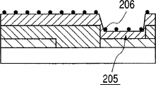
Fig. 3 A and 3B are the schematic diagrames of an example that the structure of the electronic emission element that is obtained by the present invention is shown, and Fig. 3 A is a plane graph, and Fig. 3 B is the a-a profile of Fig. 3 A.
In Fig. 3 A and 3B, 201 show the substrate of insulating properties, and 202 show the 2nd electrode (control electrode or extraction electrode), and 203 show the 1st electrode (cathode electrode), and 205 show conductive material layer, and 207 show the carbon fiber as emitter material.
As the substrate 201 of insulating properties, as having illustrated among Figure 1A to Fig. 1 C-2, can use the sheet material of the electrical insulating property of quartz glass etc., cleaned its surface fully and used.
The material that can use as cathode electrode 203, conductive material layer 205, with the material of the cathode electrode 103 that in Figure 1A to Fig. 1 C-2, has illustrated, conductive material layer 105 be same.In addition, in this embodiment, depend on the material of employed particle, conductive material layer 205 not necessarily needs configuration, but preferably uses conductive material layer 205.Moreover, as the material of electrode 202, can use the material same with cathode electrode 203.
As the carbon fiber 207 of emitter material,, be to use the carbon fiber of particle 206 (with reference to Fig. 2 A to 2E-2) growth as having illustrated among Figure 1A to Fig. 1 C-2.
Below, illustrate by each operation.
(operation 1)
After having cleaned substrate 201 fully,, at first on the whole surface of substrate 201, cover and form not shown electrode layer in order to form electrode 202 and cathode electrode 203.
Secondly, in photo-mask process, use not shown positive light anti-etching agent to form the resist figure, the above-mentioned photoresist of composition is carried out dry etching as mask, electrode gap (width in interelectrode gap) is decided to be several microns (for example 5 microns), electrode 202 and cathode electrode 203 are carried out composition (Fig. 2 A).
Below, with photo-mask process, film forming, peel off, the film of etching etc. or the composition of resist simply be called composition.
(operation 2)
Carry out composition (Fig. 2 B) to peeling off peeling off that later upper layer uses with metal (for example Cr) 204.
Secondly, form conductive material layer 205.Then, the dispersion liquid that applies particle 206 is thereon filmed with configuration.Then, film, remove (evaporation) at least and disperse media (with anti-agglutinant), a plurality of particles 206 are set on conductive material layer 205 dispersedly by heating this.At this moment, using under the situation of dispersion liquid as above-mentioned dispersion liquid of adding anti-agglutinant, as shown in Fig. 2 C-1, for particle 206, roughly in dispersion liquid, be set up under the substantially inagglutinable situation of dispersed particle one by one on the substrate 201 spaced-apart certain intervals.In addition, do not add anti-agglutinant or be lower than under the situation of dispersion liquid of amount of anti-agglutinant of above-mentioned comparatively desirable scope having used, for particle 206, spaced-apart certain compartment of terrain is provided with a plurality of particles aggegation and each agglutination body (Fig. 2 C-2) of forming on substrate 201.
Then, particularly, the atmosphere of (when particularly heating) oxidizing atmosphere preferably when removing above-mentioned dispersion media and anti-agglutinant.By in oxidizing atmosphere, heating, its surface at least of oxidizable particles 206, its result can increase the connecting airtight property of matrix (for example cathode electrode 203) and particle 206.Its result can suppress to result from a part of stripping of element of constituent particle 206 of matting etc. of the stripper that uses in the composition operation in the operation 3 described later or situation that particle 206 flows out with stripper etc.In addition, can stably carry out the growth of fiber.
(operation 3)
The stripper (etching liquid) of the metal level of peeling off usefulness 204 of use in operation 2, conductive material layer 205 in each metal level 204 on the stripping metal layer 204 and particle 206, the figure of formation conductive material layer 205 and particle 206 in desirable zone (Fig. 2 D-1,2D-2).
(operation 4)
Then, in carbonaceous gas, utilize the catalyst action of particle 206 to carry out heating and decomposition carbonaceous gas (hot CVD) processing.Use sem observation if handle the back at this, then formed as can be known carbon fiber 207 (Fig. 2 E-1,2E-2).In addition, in above-mentioned operation 2, under the situation of the oxidation operation that has increased particle 206, before carrying out above-mentioned operation 4 (operation that is through with 3 back), preferably increase the operation of going back primary particle 206 (for example operation that in the reducibility gas of hydrogen etc., heats).In addition, also can carry out above-mentioned reduction operation with above-mentioned operation 4 (making carbon fibre growth).That is, can in above-mentioned carbonaceous gas, sneak into the growth operation that reducibility gas (for example hydrogen) carries out above-mentioned carbon fiber 207.Perhaps, if use the carbonaceous gas of reproducibility, then also there is no need to increase in addition reducibility gas.In addition, above-mentioned reduction operation is in order to present the catalyst action of losing because of oxidation operation once more or to improve the operation that catalyst action carries out.
In addition, the effect of above-mentioned oxidation operation is not limited to comprise the situation of the element of the particle (catalyst particle) that has catalyst action more than 2 kinds.Promptly, even under the situation of having used the particle that constitutes by single-element (the metallic element simple substance of Pd, Fe, Co, Ni etc.) with catalyst action, if used the composition of solution (also comprising stripper etc.) after having carried out above-mentioned oxidation operation, also reproducibility well, stably disposes particle.In addition, if carry out the growth operation of carbon fiber after having carried out above-mentioned oxidation operation, then can stably form the carbon fiber high with the bonding force of substrate, its result can obtain stable electron emission characteristic.In addition, such particle that constitutes by single-element with catalyst action preferably be dispersed in except that the forming of particle with the same dispersion liquid of the particle that has disperseed to constitute with catalyst action by multiple element in to be coated on the substrate.
Utilize above operation, can form electronic emission element with many carbon fibers.
In addition, on this shows surface at same substrate, disposed the example of the 1st electrode 203 (cathode electrode) and the 2nd electrode 202 (extraction electrode or control electrode), but electronic emission element of the present invention is not limited to such form.For example, also can be the form of many carbon fibers of configuration on the 1st electrode of as the Spindt type, going up the 2nd electrode (extraction electrode or control electrode) that configuration has opening, in opening, exposing at the 1st electrode (cathode electrode).More particularly, also can be the 1st electrode (cathode electrode) go up insulating barrier that configuration has the 1st opening so that on the insulating barrier stacked have with the 2nd electrode (extraction electrode or control electrode) of the 2nd opening of the 1st open communication, utilize method of the present invention to make many carbon fibre growths so as conductivity be connected to the form that disposes on the part of the 1st electrode that is arranged in the opening that the 1st and the 2nd opening forms.
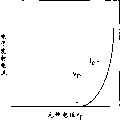
Moreover, utilize Fig. 4, Fig. 5 explanation to utilize the electron emission characteristic of the electronic emission element with many carbon fibers 207 of above-mentioned operation 1~operation 4 formation.A bit be that the 2nd electrode uses as draw the extraction electrode that electronics uses from fiber 207 by what this example will be noted.
In order to measure electron emission characteristic, at first, the gap that is provided with in the vacuum plant 408 shown in Figure 4 with several microns~tens microns has separated the 2nd electrode 202 (extraction electrode or control electrode) and Fig. 3 A of the 1st electrode 203 (cathode electrode) and the electronic emission element shown in Fig. 3 B, utilize vacuum pumping hardware 409 exhaust fully, up to making inner vacuum reach about 10
-4Pa.Then, use high-voltage power supply,, apply the high voltage Va that constitutes by several kilovolts on the position of the height H of substrate more than 201 mm, anode 410 being set.Have again, the fluorophor 411 that has covered conductive film is set on anode 410.
Then, by applying the pulse voltage that constitutes by about tens V at the 1st electrode 203 of electronic emission element and 202 at the 2nd electrode, can detect at electrode 203 and 202 mobile element current If of electrode and electron emission current Ie as driving voltage Vf.
The equipotential line of this moment is shown with dotted line 412 in Fig. 4.Can imagine the most concentrated point 413 of electric field near as the most close anode 410 of the carbon fiber 207 of electronic emission material, and be in electrode 203 and electrode 202 the gap near, can think from this emitting electrons consumingly.
As the electron emission characteristic that utilizes configuration detection as described above, can obtain the characteristic shown in Fig. 5.Promptly, if Vf (voltage that is applied between electrode 203 and electrode 202) is increased, then Ie (emission current) rises sharp, and not shown If (electric current that flows between electrode 203 and electrode 202) is similar to the characteristic of Ie, but its value and Ie relatively become enough little value.In addition, do not use in the form of gate electrode 202 even dispose anode electrode above the substrate shown in Figure 1A to 1C-2 101, this electron emission characteristic also is same.
Below, use Fig. 6, Fig. 7 explanation to possess the image processing system that the electron source of the electronic emission element shown in a plurality of Fig. 3 A and the 3B obtains according to this principle configuration.What should note in this embodiment a bit is, the 2nd electrode 202 uses as draw the extraction electrode that electronics uses from fiber 207.
In Fig. 6, the 601st, electron source matrix, the 602nd, directions X wiring, the 603rd, the wiring of Y direction.The 604th, the electronic emission element that obtains by the present invention.
In Fig. 6, by Dx1, Dx2 ..., Dxm constitutes m bar directions X wiring 602.The suitably material of designing wiring, thickness, width.By n bar Dy1, Dy2 ..., Dyn wiring constitute Y direction wiring 603, similarly form with directions X wiring 602.Between this m bar directions X wiring 602 and n bar Y direction wiring 603, be provided with not shown interlayer insulating film, both carried out the isolation (m, n are positive integers) of conductivity.
As shown in Figure 7, be connected respectively to the last outside that is drawn out to of outside terminal Dox1~Doxm, Doy1~Doyn by directions X wiring 602 and Y direction wiring 603.In addition, at this, distinguished Dx1~Dxm (Dv1~Dvn) and Dox1~Doxm (Doy1~Doyn), but also can be respectively a continuous wiring.
The pair of electrodes (the 1st electrode 203 and electrode 202 among Fig. 3 A and the 3B) that constitutes electronic emission element 604 separately is connected to conductivity a certain of m bar directions X wiring 602 and n bar Y direction respectively and connects up on 603 a certain.
The not shown sweep signal bringing device that in directions X wiring 602, connects the sweep signal of the capable usefulness that applies the electronic emission element 604 that selection for example arranges on directions X.On the other hand, by in Y direction wiring 603, connecting respectively being listed as of electronic emission element 604 of arranging modulated the not shown modulation signal occurrence device of usefulness on the Y direction according to input signal, select other electronic emission element 604, can drive independently.
Use Fig. 7 that the image processing system that the electron source of the simple matrix configuration that use is such constitutes is described.
Fig. 7 is the figure that illustrates as the image display device (flat-panel monitor) of an example of the image processing system that is obtained by the present invention.
In Fig. 7, the 701st, disposed the electron source matrix of a plurality of electronic emission elements of the present invention 706, the 703rd, fixed the back plate of electron source matrix 701, the 710th, the header board that on the inner surface of glass basis 709, constitutes by fluorescent film 708 and metal base (metal film that constitutes by Al etc.) 707 etc.The 704th, carriage is connected with back plate 703, header board 710.The 711st, peripheral device constitutes by the bonding above-mentioned header board 710 of mutual sealing, carriage 704, back plate 703.In addition, the inside of this periphery device is retained as vacuum.
702,705 directions X that is connected with electronic emission element 706 wiring and the wirings of Y direction that are to use Fig. 6 to illustrate.
In the structure of the image processing system of this narration is to utilize an example of the image processing system that the present invention obtains, and can carry out various distortion according to technological thought of the present invention.About input signal, except NTSC mode, PAL, SECAM mode etc., also can adopt and compare TV signal (for example, in the MUSE mode being the high-grade TV of the representative) mode that constitutes by the multi-strip scanning line with aforesaid way.In addition, utilize image processing system that the present invention obtains except the display unit of display unit, video conference system or the computer etc. that can be used as television broadcasting, also can be used as the optical printer that utilizes the photonasty drum to wait to constitute etc.
[embodiment]
Below, illustrate in greater detail the present invention.
<embodiment 1 〉
Preparation consists of Pd (60atm%), Co (40atm%), average grain diameter is the alloy particle of 5nm, has formed the dispersion liquid that has disperseed this alloy particle with 0.1g/L.In above-mentioned dispersion liquid, as disperseing media, use ethanol, the PVP (polyvinylpyrrolidone) that has added 5wt% is as anti-agglutinant, so that disperse above-mentioned alloy particle with monomer.
Below, use above-mentioned dispersion liquid, explain the manufacturing process of the electronic emission element of the present embodiment shown in Fig. 2 A to 2E-2.
(operation 1)
Use quartz base plate as substrate 201, after having carried out sufficient cleaning, in order to form extraction electrode 202 and negative electrode (emitter) electrode 203, at first on whole of substrate 201, utilize sputtering method successively continuously evaporation not shown thickness be the substrate of the Ti of 5nm and thickness Pt for 100nm.
Secondly, utilize photo-mask process, use not shown positive light anti-etching agent to form the resist figure.With the above-mentioned photoresist that has carried out composition is mask, and above-mentioned Pt layer and Ti layer are carried out dry etching, is that the extraction electrode 202 and the cathode electrode 203 of 5 microns formations carried out composition (Fig. 2 A) to electrode gap.
(operation 2)
Carry out composition (Fig. 2 B) to peeling off peeling off that later upper layer uses with Metal Cr 204.
Secondly, formed the TiN layer as conductive material layer 205.
Use thereon from spigot with the condition spin coated of 2000rpm the dispersion liquid of above-mentioned alloy particle 206.After coating, utilize 350 ℃ of oxidation operations of 10 minutes in the atmosphere in cleaning in the stove, carried out disperseing the oxidation with particle of removing of media and anti-agglutinant.Peel off thereafter.
(operation 3)
Use stripper of the resist of composition in operation 2, in each Cr layer 204, peel off conductive material layer 205 and alloy particle 206 on the resist figure 204, in desirable zone, formed the figure (Fig. 2 D-1) of conductive material layer 205 and alloy particle 206.
(operation 4)
Then, in containing the atmosphere of hydrogen, carried out the reduction of particle.
Then, in the mixed atmosphere of ethene and hydrogen, under 550 degree, carried out heat treated.When after processing, having carried out observation, confirmed sparsely roughly to have formed one by one carbon fiber 207 (Fig. 2 E-1) with scanning electron microscopy.
Above such electronic emission element of making is provided with in the vacuum plant shown in Figure 4 408, utilizes vacuum pumping hardware 409 exhaust fully, up to reaching about 2 * 10
-5Pa is to having applied Va=10KV as anode voltage from substrate 201 for the anode 411 of H=2mm.At this moment, electronic emission element is applied the pulse voltage that is made of driving voltage Vf=20V, detected the element current And if the electron emission current Ie that are flowed.
The If of element, Ie characteristic are the characteristics shown in Fig. 5.That is, if surpass threshold voltage, then Ie increases sharp, when Vf is 15V, has measured the electron emission current Ie of about 1 μ A.On the other hand, the property class of If is similar to the characteristic of Ie, but its value and the Ie value that the order of magnitude is above that has been little relatively.
In addition, the situation intensive with making carbon fiber 207 compared, and can apply electric field effectively, can reduce threshold value (electronics emission) voltage.
<embodiment 2 〉
Used with 0.1g/L and disperseed to consist of Pd (60atm%), Co (40atm%), average grain diameter dispersion liquid as the alloy particle of 8nm.Use pure water as disperseing media, do not use the anti-agglutinant that in embodiment 1, uses, made the dispersion liquid of alloy particle for several agglutination bodies to tens.
In the present embodiment, carried out as described below having carried out the making of electronic emission element similarly to Example 1 beyond the operation 2 among the embodiment 1.
(operation 2)
Carry out composition (Fig. 2 B) to peeling off peeling off that later upper layer uses with Metal Cr 204.
Secondly, formed the TiN layer as the conductive material layer 205 that makes carbon fiber 207 growths through alloy particle 206.
Use thereon from spigot with the condition spin coated of 3000rpm the dispersion liquid of above-mentioned alloy particle 206.After coating, utilize 350 ℃ of oxidation operations of 10 minutes in the atmosphere, carried out disperseing the oxidation operation with particle removed of media and anti-agglutinant.Peel off thereafter.
The reduction of the particle in having carried out containing the atmosphere of hydrogen is handled the back and has been carried out after the heat treated in the mixed atmosphere of ethene and hydrogen, when having carried out observation, confirmed that carbon fiber 207 is that 1 unit has sparsely carried out the situation (Fig. 2 E-2) that growth forms with several to tens bundle with scanning electron microscopy.But, on the other hand, also there is the big agglutination body of alloy particle, as a whole, the uniformity of the density of carbon fiber has reduced.
Similarly to Example 1, the If of resulting electronic emission element, Ie characteristic are the characteristics shown in Fig. 5.That is, if surpass threshold voltage, then Ie increases sharp, when Vf is 15V, has measured the electron emission current Ie of about 1 μ A.On the other hand, the property class of If is similar to the characteristic of Ie, but its value and the Ie value that the order of magnitude is above that has been little relatively.
In addition, compare with the situation that has formed carbon fiber under the high state of in the past Particle Density, can apply electric field effectively, can reduce threshold value (electronics emission) voltage, but compare with the electronic emission element that makes in embodiment 1, the reproducibility of characteristic has reduced.
<embodiment 3 〉
Prepared with 0.1g/L disperseed to consist of Pd (70atm%), Co (30atm%), average grain diameter is the dispersion liquid of the alloy particle of 10nm.Use isopropyl alcohol as disperseing media.In addition, in the present embodiment, the PVA (polyvinyl alcohol) that has added 10wt% in dispersion liquid is as anti-agglutinant, so that disperse above-mentioned alloy particle with monomer.
In the present embodiment, carried out as described below having carried out the making of electronic emission element similarly to Example 1 beyond the operation 2 among the embodiment 1.
(operation 2)
Carry out composition (Fig. 2 B) to peeling off peeling off that later upper layer uses with Metal Cr 204.
Secondly, formed the TiN layer as conductive material layer 205.
Use the top from substrate 201 to apply the dispersion liquid of above-mentioned alloy particle 206 thereon from spigot.After coating, utilize 350 ℃ of oxidation operations of 10 minutes in the atmosphere in cleaning in the stove, carried out disperseing the oxidation with particle of removing of media and anti-agglutinant.Peel off thereafter.
Carried out the heat treated of 550 degree in the mixed atmosphere of acetylene and hydrogen after, if observe with scanning electron microscopy, having confirmed sparsely roughly grows has one by one formed carbon fiber 207 (Fig. 2 E-1).
Similarly to Example 1, the If of resulting electronic emission element, Ie characteristic are the characteristics shown in Fig. 5.That is, if surpass threshold voltage, then Ie increases sharp, when Vf is 15V, has measured the electron emission current Ie of about 1 μ A.
Compare with the situation of intensive carbon fiber 207, can apply electric field effectively, can reduce threshold value (electronics emission) voltage.
As above illustrated, in the manufacture method of the electronic emission element that has used the carbon fiber that adopts the particle that comprises the different element more than 2 kinds of the present invention, do not need the high-temperature alloy operation on the substrate, can stably and well make carbon fibre growth at low temperatures, can easily obtain using the electronic emission element of carbon fiber.In addition, owing to can make at low temperatures, so can prevent the harmful effect or the manufacturing cost rising of member that cause because of heating to other.
Moreover, by in having disperseed above-mentioned dispersion of nano-particles liquid, adding anti-agglutinant (macromolecule), can easily adjust the density that is provided with of the concentration of particle or particle, can more effectively be applied to necessary electric field in the electronics emission to carbon fiber.Thus, the threshold voltage of electronics emission is descended, can reduce the necessary electric field that the electron emission current that obtains identical value is used.
Moreover, if alloy particle that is made of Pd and specific interpolation element is used as catalyst, then can eliminate the danger of dust outburst, the antiknock device that does not only need manufacturing installation, and can prevent to become the change of shape of particle with shape bigger than initial condition, can prevent the rising of the threshold value of the rising of growth temperature of carbon fiber or electronics emission.
Claims (28)
1. manufacture method with electronic emission element of carbon fiber is characterized in that having:
(A) coating comprises the operation of liquid of a plurality of dispersed particles on substrate;
(B) the above-mentioned particle that disposes on to aforesaid substrate carries out the operation of reducing again after the oxidation; And
(C) by making carbonaceous gas contact the operation that forms carbon fiber with the above-mentioned particle that has been reduced, wherein, above-mentioned particle comprises 2 kinds of elements respectively at least.
2. the manufacture method of the electronic emission element described in claim 1 is characterized in that:
Above-mentioned particle is the alloy of above-mentioned element more than at least 2 kinds.
3. the manufacture method of the electronic emission element described in claim 1 is characterized in that:
At least a element that above-mentioned element more than at least 2 kinds is selected by Pd with from Fe, Co, Ni, Y, Rh, Pt, La, Ce, Pr, Nd, Gd, Tb, Dy, Ho, Er, Lu constitutes.
4. the manufacture method of the electronic emission element described in claim 3 is characterized in that:
It is at least a element of selecting from Fe, Co, Ni, Y, Rh, Pt, La, Ce, Pr, Nd, Gd, Tb, Dy, Ho, Er, Lu of 80atm% (atomic percentage) more than the 5atm% that above-mentioned particle contains with respect to Pd.
5. the manufacture method of the electronic emission element described in claim 1 is characterized in that:
Aforesaid liquid also comprises macromolecule.
6. the manufacture method of the electronic emission element described in claim 5 is characterized in that:
Above-mentioned macromolecule is water miscible macromolecule.
7. the manufacture method of the electronic emission element described in claim 5 is characterized in that:
Above-mentioned macromolecule is a certain of polyvinylpyrrolidone, polyvinyl alcohol, polyacrylic.
8. the manufacture method of the electronic emission element described in claim 7 is characterized in that:
Above-mentioned polyacrylic is a certain in polyacrylic acid, polymethylacrylic acid and their homolog.
9. the manufacture method of the electronic emission element described in claim 5 is characterized in that:
With respect to aforesaid liquid, it is above to the above-mentioned macromolecule below the 30wt% to comprise 0.1wt%.
10. the manufacture method of the electronic emission element described in claim 5 is characterized in that:
With respect to aforesaid liquid, it is above to the above-mentioned macromolecule below the 10wt% to comprise 0.2wt%.
11. the manufacture method of the electronic emission element described in claim 1 is characterized in that:
The average grain diameter of above-mentioned particle is that 1nm is above to 100nm.
12. the manufacture method of the electronic emission element described in claim 1 is characterized in that:
The average grain diameter of above-mentioned particle is that 1nm is above to 50nm.
13. the manufacture method of the electronic emission element described in claim 1 is characterized in that:
The average grain diameter of above-mentioned particle is that 1nm is above to 20nm.
14. the manufacture method of the electronic emission element described in claim 5 is characterized in that:
Above-mentioned macromolecule is to cover above-mentioned particle more than the 2.5nm to the scope below the 25nm at average film thickness.
15. the manufacture method of the electronic emission element described in claim 1 is characterized in that:
With respect to aforesaid liquid, comprise above-mentioned particle with the ratio below the 1g/L.
16. the manufacture method of the electronic emission element described in claim 1 is characterized in that:
With respect to aforesaid liquid, comprise above-mentioned particle with the ratio below the 0.1g/L.
17. the manufacture method of the electronic emission element described in claim 15 is characterized in that:
With respect to aforesaid liquid, comprise above-mentioned particle with the ratio more than the 0.01g/L.
18. the manufacture method of the electronic emission element described in claim 1 is characterized in that:
Aforesaid liquid also comprises photosensitive material, and operation (A) also comprises the irradiation area that operation and removing that irradiation is coated with diaphragm area films or the operation of non-irradiation area.
19. the manufacture method with electronic emission element of carbon fiber is characterized in that having:
(A) coating comprises the operation of liquid of the dispersed particle with catalyst function on substrate;
(B) operation of the above-mentioned particle that on aforesaid substrate, disposes of oxidation; And
(C) reduction above-mentioned particle and make the above-mentioned operation that primary particle contacts with carbonaceous gas of going back.
20. a manufacture method of having used the electronic emission element of carbon fiber is characterized in that having:
(A) coating is dispersed with a plurality of operations of liquid that comprise macromolecule and comprise the particle of catalyst metals on substrate;
The operation of a plurality of particles that comprise above-mentioned catalyst metals that (B) oxidation is disposed on aforesaid substrate; And
(C) by reducing above-mentioned oxidized catalyst particle and make it contact the operation that forms carbon fiber with carbonaceous gas.
21. the manufacture method of the electronic emission element described in claim 1 is characterized in that:
Above-mentioned carbon fiber is a certain of carbon nano-tube, gnf, amorphous carbon fiber, diamond fiber.
22. the manufacture method with electron source of a plurality of electronic emission elements is characterized in that:
Utilize the manufacture method of the electronic emission element described in the claim 1~21 to make this electronic emission element.
23. the manufacture method of an image processing system, this image processing system have electron source and the image that relatively disposes with this electron source forms member, it is characterized in that:
Utilize the manufacture method of the electron source described in the claim 22 to make above-mentioned electron source.
24. make the China ink that carbon fiber is used for one kind, it is characterized in that having:
The particle that comprises the element more than at least 2 kinds;
Macromolecule; And
Disperse above-mentioned dispersion of nano-particles media.
25. the China ink that the manufacturing carbon fiber described in claim 24 is used is characterized in that:
At least a element that above-mentioned element more than at least 2 kinds is selected by Pd with from Fe, Co, Ni, Y, Rh, Pt, La, Ce, Pr, Nd, Gd, Tb, Dy, Ho, Er, Lu constitutes.
26. the China ink that the manufacturing carbon fiber described in claim 24 is used is characterized in that:
Above-mentioned macromolecule is a certain of polyvinylpyrrolidone, polyvinyl alcohol, polyacrylic.
27. the China ink that the manufacturing carbon fiber described in each of claim 24~26 is used is characterized in that:
With respect to above-mentioned China ink, it is above to the above-mentioned macromolecule below the 30wt% to comprise 0.1wt%.
28. the China ink that the manufacturing carbon fiber described in each of claim 24~26 is used is characterized in that:
The average grain diameter of above-mentioned particle is that 1nm is above to 100nm.
Applications Claiming Priority (4)
| Application Number | Priority Date | Filing Date | Title |
|---|---|---|---|
| JP280420/2002 | 2002-09-26 | ||
| JP2002280420 | 2002-09-26 | ||
| JP2003306158A JP3625467B2 (en) | 2002-09-26 | 2003-08-29 | Electron emitting device using carbon fiber, electron source, and method of manufacturing image forming apparatus |
| JP306158/2003 | 2003-08-29 |
Publications (2)
| Publication Number | Publication Date |
|---|---|
| CN1497639A true CN1497639A (en) | 2004-05-19 |
| CN100361258C CN100361258C (en) | 2008-01-09 |
Family
ID=32032903
Family Applications (1)
| Application Number | Title | Priority Date | Filing Date |
|---|---|---|---|
| CNB031598447A Expired - Fee Related CN100361258C (en) | 2002-09-26 | 2003-09-26 | Manufacturing method of electronic transmitting element, electronic source and image forming device using carbon fibre, ink made of carbon fibre |
Country Status (3)
| Country | Link |
|---|---|
| US (1) | US7147533B2 (en) |
| JP (1) | JP3625467B2 (en) |
| CN (1) | CN100361258C (en) |
Cited By (2)
| Publication number | Priority date | Publication date | Assignee | Title |
|---|---|---|---|---|
| CN101496114B (en) * | 2006-07-29 | 2012-11-28 | 肖克科技有限公司 | Voltage switchable dielectric material having conductive or semi-conductive organic material |
| CN107275648A (en) * | 2016-04-06 | 2017-10-20 | 格林纳瑞缇有限公司 | For the method and apparatus for the film for preparing catalyst coating |
Families Citing this family (57)
| Publication number | Priority date | Publication date | Assignee | Title |
|---|---|---|---|---|
| US20100038121A1 (en) * | 1999-08-27 | 2010-02-18 | Lex Kosowsky | Metal Deposition |
| US20100038119A1 (en) * | 1999-08-27 | 2010-02-18 | Lex Kosowsky | Metal Deposition |
| WO2001017320A1 (en) * | 1999-08-27 | 2001-03-08 | Lex Kosowsky | Current carrying structure using voltage switchable dielectric material |
| US20080035370A1 (en) * | 1999-08-27 | 2008-02-14 | Lex Kosowsky | Device applications for voltage switchable dielectric material having conductive or semi-conductive organic material |
| JP3768908B2 (en) * | 2001-03-27 | 2006-04-19 | キヤノン株式会社 | Electron emitting device, electron source, image forming apparatus |
| JP3619240B2 (en) * | 2002-09-26 | 2005-02-09 | キヤノン株式会社 | Method for manufacturing electron-emitting device and method for manufacturing display |
| US7064475B2 (en) * | 2002-12-26 | 2006-06-20 | Canon Kabushiki Kaisha | Electron source structure covered with resistance film |
| JP3907626B2 (en) * | 2003-01-28 | 2007-04-18 | キヤノン株式会社 | Manufacturing method of electron source, manufacturing method of image display device, manufacturing method of electron-emitting device, image display device, characteristic adjustment method, and characteristic adjustment method of image display device |
| JP3697257B2 (en) | 2003-03-25 | 2005-09-21 | キヤノン株式会社 | Carbon fiber, electron-emitting device, electron source, image forming apparatus, light valve, and secondary battery manufacturing method |
| JP3763078B2 (en) * | 2003-06-02 | 2006-04-05 | 松下電器産業株式会社 | Electron emitting material and manufacturing method thereof |
| US7202596B2 (en) * | 2003-06-06 | 2007-04-10 | Electrovac Ag | Electron emitter and process of fabrication |
| JP4324078B2 (en) * | 2003-12-18 | 2009-09-02 | キヤノン株式会社 | Carbon-containing fiber, substrate using carbon-containing fiber, electron-emitting device, electron source using the electron-emitting device, display panel using the electron source, and information display / reproduction device using the display panel, And production methods thereof |
| JP2005190889A (en) * | 2003-12-26 | 2005-07-14 | Canon Inc | Electron emitting element, electron source, image display device and manufacturing methods for them |
| US20050279274A1 (en) * | 2004-04-30 | 2005-12-22 | Chunming Niu | Systems and methods for nanowire growth and manufacturing |
| JP3935479B2 (en) * | 2004-06-23 | 2007-06-20 | キヤノン株式会社 | Carbon fiber manufacturing method, electron-emitting device manufacturing method using the same, electronic device manufacturing method, image display device manufacturing method, and information display / reproducing apparatus using the image display device |
| JP4596878B2 (en) | 2004-10-14 | 2010-12-15 | キヤノン株式会社 | Structure, electron-emitting device, secondary battery, electron source, image display device, information display / reproduction device, and manufacturing method thereof |
| KR100682952B1 (en) * | 2005-08-31 | 2007-02-15 | 삼성전자주식회사 | Nano-elastic memory device and method of manufacturing the same |
| US7824495B1 (en) | 2005-11-09 | 2010-11-02 | Ut-Battelle, Llc | System to continuously produce carbon fiber via microwave assisted plasma processing |
| US20100264225A1 (en) * | 2005-11-22 | 2010-10-21 | Lex Kosowsky | Wireless communication device using voltage switchable dielectric material |
| EP1969627A4 (en) | 2005-11-22 | 2010-01-20 | Shocking Technologies Inc | Semiconductor devices including voltage switchable materials for over-voltage protection |
| CN100573778C (en) * | 2006-07-07 | 2009-12-23 | 清华大学 | Field-transmitting cathode and manufacture method thereof |
| JP2008027853A (en) * | 2006-07-25 | 2008-02-07 | Canon Inc | Electron emitting element, electron source, image display device, and method of manufacturing them |
| US7968014B2 (en) * | 2006-07-29 | 2011-06-28 | Shocking Technologies, Inc. | Device applications for voltage switchable dielectric material having high aspect ratio particles |
| US20080029405A1 (en) * | 2006-07-29 | 2008-02-07 | Lex Kosowsky | Voltage switchable dielectric material having conductive or semi-conductive organic material |
| US20080032049A1 (en) * | 2006-07-29 | 2008-02-07 | Lex Kosowsky | Voltage switchable dielectric material having high aspect ratio particles |
| US7879131B2 (en) * | 2006-08-15 | 2011-02-01 | Applied Nanotech Holdings, Inc. | Metal encapsulation |
| JP2010504437A (en) * | 2006-09-24 | 2010-02-12 | ショッキング テクノロジーズ インコーポレイテッド | Techniques for plating substrate devices using voltage-switchable dielectric materials and light assistance |
| WO2008036423A2 (en) | 2006-09-24 | 2008-03-27 | Shocking Technologies, Inc. | Formulations for voltage switchable dielectric material having a stepped voltage response and methods for making the same |
| US20120119168A9 (en) * | 2006-11-21 | 2012-05-17 | Robert Fleming | Voltage switchable dielectric materials with low band gap polymer binder or composite |
| US20080169003A1 (en) * | 2007-01-17 | 2008-07-17 | Nasa Headquarters | Field reactive amplification controlling total adhesion loading |
| US20090050856A1 (en) * | 2007-08-20 | 2009-02-26 | Lex Kosowsky | Voltage switchable dielectric material incorporating modified high aspect ratio particles |
| US8206614B2 (en) | 2008-01-18 | 2012-06-26 | Shocking Technologies, Inc. | Voltage switchable dielectric material having bonded particle constituents |
| US20090220771A1 (en) * | 2008-02-12 | 2009-09-03 | Robert Fleming | Voltage switchable dielectric material with superior physical properties for structural applications |
| EP2109132A3 (en) * | 2008-04-10 | 2010-06-30 | Canon Kabushiki Kaisha | Electron beam apparatus and image display apparatus using the same |
| EP2109131B1 (en) | 2008-04-10 | 2011-10-26 | Canon Kabushiki Kaisha | Electron emitter and electron beam apparatus and image display apparatus using said emitter |
| JP2009277457A (en) * | 2008-05-14 | 2009-11-26 | Canon Inc | Electron emitting element, and image display apparatus |
| JP2009277460A (en) * | 2008-05-14 | 2009-11-26 | Canon Inc | Electron-emitting device and image display apparatus |
| US20100047535A1 (en) * | 2008-08-22 | 2010-02-25 | Lex Kosowsky | Core layer structure having voltage switchable dielectric material |
| JP4458380B2 (en) * | 2008-09-03 | 2010-04-28 | キヤノン株式会社 | Electron emitting device, image display panel using the same, image display device, and information display device |
| US20100065785A1 (en) * | 2008-09-17 | 2010-03-18 | Lex Kosowsky | Voltage switchable dielectric material containing boron compound |
| JP2010073470A (en) * | 2008-09-18 | 2010-04-02 | Canon Inc | Image display apparatus |
| US9208931B2 (en) * | 2008-09-30 | 2015-12-08 | Littelfuse, Inc. | Voltage switchable dielectric material containing conductor-on-conductor core shelled particles |
| CN102246246A (en) * | 2008-09-30 | 2011-11-16 | 肖克科技有限公司 | Voltage switchable dielectric material containing conductive core shelled particles |
| US8399773B2 (en) | 2009-01-27 | 2013-03-19 | Shocking Technologies, Inc. | Substrates having voltage switchable dielectric materials |
| US8272123B2 (en) | 2009-01-27 | 2012-09-25 | Shocking Technologies, Inc. | Substrates having voltage switchable dielectric materials |
| US9226391B2 (en) | 2009-01-27 | 2015-12-29 | Littelfuse, Inc. | Substrates having voltage switchable dielectric materials |
| KR101679099B1 (en) | 2009-03-26 | 2016-11-23 | 쇼킹 테크놀로지스 인코포레이티드 | Components having voltage switchable dielectric materials |
| US8623288B1 (en) | 2009-06-29 | 2014-01-07 | Nanosys, Inc. | Apparatus and methods for high density nanowire growth |
| WO2011060017A2 (en) | 2009-11-11 | 2011-05-19 | Amprius, Inc | Intermediate layers for electrode fabrication |
| US20110198544A1 (en) * | 2010-02-18 | 2011-08-18 | Lex Kosowsky | EMI Voltage Switchable Dielectric Materials Having Nanophase Materials |
| US9320135B2 (en) * | 2010-02-26 | 2016-04-19 | Littelfuse, Inc. | Electric discharge protection for surface mounted and embedded components |
| US9224728B2 (en) * | 2010-02-26 | 2015-12-29 | Littelfuse, Inc. | Embedded protection against spurious electrical events |
| US9082622B2 (en) | 2010-02-26 | 2015-07-14 | Littelfuse, Inc. | Circuit elements comprising ferroic materials |
| WO2013006583A2 (en) | 2011-07-01 | 2013-01-10 | Amprius, Inc. | Template electrode structures with enhanced adhesion characteristics |
| RU2521436C1 (en) * | 2013-01-09 | 2014-06-27 | Открытое акционерное общество "Научно-исследовательский институт газоразрядных приборов "Плазма" (ОАО "Плазма") | Pulsed x-ray tube |
| US20170283629A1 (en) * | 2016-03-29 | 2017-10-05 | University Of North Texas | Metal-based ink for additive manufacturing process |
| US11913146B1 (en) * | 2019-07-18 | 2024-02-27 | United States Of America As Represented By The Secretary Of The Air Force | Carbon nanotube yarn cathode using textile manufacturing methods |
Family Cites Families (39)
| Publication number | Priority date | Publication date | Assignee | Title |
|---|---|---|---|---|
| US5171560A (en) * | 1984-12-06 | 1992-12-15 | Hyperion Catalysis International | Carbon fibrils, method for producing same, and encapsulated catalyst |
| US4948573A (en) * | 1986-12-02 | 1990-08-14 | Alcan International Limited | Process for producing silicon carbide and metal carbides |
| US4904895A (en) * | 1987-05-06 | 1990-02-27 | Canon Kabushiki Kaisha | Electron emission device |
| US4900483A (en) * | 1987-10-29 | 1990-02-13 | Exxon Research And Engineering Company | Method of producing isotropically reinforced net-shape microcomposites |
| JP2721075B2 (en) | 1992-04-09 | 1998-03-04 | シャープ株式会社 | Method for producing vapor grown carbon fiber |
| JPH0765708A (en) | 1993-08-25 | 1995-03-10 | Canon Inc | Manufacture of electron emission element and image formng device |
| JP3072825B2 (en) * | 1994-07-20 | 2000-08-07 | キヤノン株式会社 | Electron emitting element, electron source, and method of manufacturing image forming apparatus |
| JP3332676B2 (en) * | 1994-08-02 | 2002-10-07 | キヤノン株式会社 | Electron emitting element, electron source, image forming apparatus, and method of manufacturing them |
| US6246168B1 (en) * | 1994-08-29 | 2001-06-12 | Canon Kabushiki Kaisha | Electron-emitting device, electron source and image-forming apparatus as well as method of manufacturing the same |
| EP1037246B1 (en) * | 1994-09-22 | 2004-03-10 | Canon Kabushiki Kaisha | Method of manufacturing an electron-emitting device as well as an electron source and an image forming apparatus comprising such electron-emitting devices |
| JP2903290B2 (en) | 1994-10-19 | 1999-06-07 | キヤノン株式会社 | Method for manufacturing electron-emitting device, electron source using the electron-emitting device, and image forming apparatus |
| JP2932250B2 (en) * | 1995-01-31 | 1999-08-09 | キヤノン株式会社 | Electron-emitting device, electron source, image forming apparatus, and manufacturing method thereof |
| JP3174999B2 (en) * | 1995-08-03 | 2001-06-11 | キヤノン株式会社 | Electron emitting element, electron source, image forming apparatus using the same, and method of manufacturing the same |
| US5872422A (en) * | 1995-12-20 | 1999-02-16 | Advanced Technology Materials, Inc. | Carbon fiber-based field emission devices |
| JP3441923B2 (en) | 1997-06-18 | 2003-09-02 | キヤノン株式会社 | Manufacturing method of carbon nanotube |
| JP3740295B2 (en) * | 1997-10-30 | 2006-02-01 | キヤノン株式会社 | Carbon nanotube device, manufacturing method thereof, and electron-emitting device |
| JP3363759B2 (en) | 1997-11-07 | 2003-01-08 | キヤノン株式会社 | Carbon nanotube device and method of manufacturing the same |
| JP3631015B2 (en) * | 1997-11-14 | 2005-03-23 | キヤノン株式会社 | Electron emitting device and manufacturing method thereof |
| JP2000200544A (en) | 1999-01-08 | 2000-07-18 | Canon Inc | Manufacture of electron emitting element, and manufacture of electron source and image forming device |
| JP2000311587A (en) * | 1999-02-26 | 2000-11-07 | Canon Inc | Electron emitting device and image forming device |
| US6333016B1 (en) * | 1999-06-02 | 2001-12-25 | The Board Of Regents Of The University Of Oklahoma | Method of producing carbon nanotubes |
| KR20010082591A (en) | 1999-12-21 | 2001-08-30 | 이데이 노부유끼 | Electron emission device, cold cathode field emission device and method for the production thereof, and cold cathode field emission display and method for the production thereof |
| JP2002197965A (en) | 1999-12-21 | 2002-07-12 | Sony Corp | Electron emitting device, cold cathode field electron emitting element and its manufacturing method, and cold cathode field electron emission display device and its manufacturing method |
| JP3953276B2 (en) | 2000-02-04 | 2007-08-08 | 株式会社アルバック | Graphite nanofiber, electron emission source and manufacturing method thereof, display element having the electron emission source, and lithium ion secondary battery |
| KR20030047888A (en) | 2000-05-26 | 2003-06-18 | 이 아이 듀폰 디 네모아 앤드 캄파니 | Catalytically Grown Carbon Fiber Field Emitters and Field Emitter Cathodes Made Therefrom |
| JP3463091B2 (en) | 2000-08-29 | 2003-11-05 | 独立行政法人産業技術総合研究所 | Method for producing carbon nanotube |
| JP3610325B2 (en) * | 2000-09-01 | 2005-01-12 | キヤノン株式会社 | Electron emitting device, electron source, and method of manufacturing image forming apparatus |
| JP3658346B2 (en) | 2000-09-01 | 2005-06-08 | キヤノン株式会社 | Electron emitting device, electron source and image forming apparatus, and method for manufacturing electron emitting device |
| JP3639809B2 (en) * | 2000-09-01 | 2005-04-20 | キヤノン株式会社 | ELECTRON EMITTING ELEMENT, ELECTRON EMITTING DEVICE, LIGHT EMITTING DEVICE, AND IMAGE DISPLAY DEVICE |
| JP3639808B2 (en) * | 2000-09-01 | 2005-04-20 | キヤノン株式会社 | Electron emitting device, electron source, image forming apparatus, and method of manufacturing electron emitting device |
| JP3634781B2 (en) * | 2000-09-22 | 2005-03-30 | キヤノン株式会社 | Electron emission device, electron source, image forming device, and television broadcast display device |
| CN1207185C (en) * | 2000-09-26 | 2005-06-22 | 天津南开戈德集团有限公司 | Prepn of nano-carbon tube |
| JP3768908B2 (en) * | 2001-03-27 | 2006-04-19 | キヤノン株式会社 | Electron emitting device, electron source, image forming apparatus |
| US20030222560A1 (en) * | 2001-05-22 | 2003-12-04 | Roach David Herbert | Catalytically grown carbon fiber field emitters and field emitter cathodes made therefrom |
| JP3703415B2 (en) | 2001-09-07 | 2005-10-05 | キヤノン株式会社 | ELECTRON EMITTING ELEMENT, ELECTRON SOURCE, IMAGE FORMING APPARATUS, AND METHOD FOR MANUFACTURING ELECTRON EMITTING ELEMENT AND ELECTRON SOURCE |
| JP3605105B2 (en) * | 2001-09-10 | 2004-12-22 | キヤノン株式会社 | Electron emitting element, electron source, light emitting device, image forming apparatus, and method of manufacturing each substrate |
| JP3710436B2 (en) * | 2001-09-10 | 2005-10-26 | キヤノン株式会社 | Electron emitting device, electron source, and manufacturing method of image display device |
| JP3768937B2 (en) * | 2001-09-10 | 2006-04-19 | キヤノン株式会社 | Electron emitting device, electron source, and manufacturing method of image display device |
| JP3619240B2 (en) * | 2002-09-26 | 2005-02-09 | キヤノン株式会社 | Method for manufacturing electron-emitting device and method for manufacturing display |
-
2003
- 2003-08-29 JP JP2003306158A patent/JP3625467B2/en not_active Expired - Fee Related
- 2003-09-15 US US10/661,627 patent/US7147533B2/en not_active Expired - Fee Related
- 2003-09-26 CN CNB031598447A patent/CN100361258C/en not_active Expired - Fee Related
Cited By (3)
| Publication number | Priority date | Publication date | Assignee | Title |
|---|---|---|---|---|
| CN101496114B (en) * | 2006-07-29 | 2012-11-28 | 肖克科技有限公司 | Voltage switchable dielectric material having conductive or semi-conductive organic material |
| CN107275648A (en) * | 2016-04-06 | 2017-10-20 | 格林纳瑞缇有限公司 | For the method and apparatus for the film for preparing catalyst coating |
| CN107275648B (en) * | 2016-04-06 | 2022-02-18 | 格林纳瑞缇有限公司 | Method and apparatus for preparing catalyst coated membranes |
Also Published As
| Publication number | Publication date |
|---|---|
| JP2004139973A (en) | 2004-05-13 |
| JP3625467B2 (en) | 2005-03-02 |
| US7147533B2 (en) | 2006-12-12 |
| US20040063839A1 (en) | 2004-04-01 |
| CN100361258C (en) | 2008-01-09 |
Similar Documents
| Publication | Publication Date | Title |
|---|---|---|
| CN1497639A (en) | Manufacturing method of electronic transmitting element, electronic source and image forming device using carbon fibre, ink made of carbon fibre | |
| CN1195312C (en) | Electron emitting equipment, electron emitting device, image display device and light emitting device | |
| CN1252329C (en) | Carbon fiber mfg. method and its use, and ink for producing catalyst | |
| CN1246513C (en) | Electronic transmitting and electron source, and fiber and image display device manufacture method | |
| CN1275845C (en) | Hollow graphite flake structure, electrode structure, its producing process and device produced thereof | |
| CN1339810A (en) | Electronic transmitting device, electron source, image forming device, method for producing electronic transmitting device and electronic transmitter | |
| CN1240095C (en) | Electronic transmitting element, electron source, image display device and manufacture method thereof | |
| US8058787B2 (en) | Carbon-fiber web structure type field emitter electrode and fabrication method of the same | |
| CN1712351A (en) | Method for manufacturing carbon fibers and use thereof | |
| CN1643636A (en) | Field emission devices using modified carbon nanotubes | |
| EP1643020A1 (en) | Catalyst used to form carbon fiber, method of making the same and uses | |
| CN1215518C (en) | Electronic transmitting device electronic source and method for manufacturing image forming device | |
| CN1722345A (en) | Method for manufacturing electron-emitting device, methods for manufacturing electron source and image display device | |
| CN1396617A (en) | Electron emission element, electronic source and image forming device | |
| JP2008509540A (en) | Field emission backlight for LCD TV | |
| CN1929072A (en) | Process for fabricating electron emitting device, electron source, and image display device | |
| CN1691242A (en) | Electron-emitting device, electron source, and method for manufacturing image displaying apparatus | |
| CN1667781A (en) | Electron-emitting device, method of manufacturing the same and application thereof | |
| CN1199218C (en) | Method for creating field electron emission material and field electron emitter comprising said material | |
| CN1306537C (en) | Electronic device, electronic source and mfg. method for electronic device | |
| CN1637998A (en) | Electron-emitting device manufacturing method, electron source manufacturing method, image-forming apparatus manufacturing method, and information displaying and playing apparatus manufacturing method | |
| CN1691243A (en) | Field emission device | |
| US20220399177A1 (en) | Carbon nanotube (cnt) paste emitter, method of manufacturing the same, and x-ray tube apparatus using the same | |
| JP3897794B2 (en) | Method for manufacturing electron-emitting device, electron source, and image forming apparatus | |
| CN1725415A (en) | Electron-emitting device, electron source, image display apparatus, and television apparatus |
Legal Events
| Date | Code | Title | Description |
|---|---|---|---|
| C06 | Publication | ||
| PB01 | Publication | ||
| C10 | Entry into substantive examination | ||
| SE01 | Entry into force of request for substantive examination | ||
| C14 | Grant of patent or utility model | ||
| GR01 | Patent grant | ||
| C17 | Cessation of patent right | ||
| CF01 | Termination of patent right due to non-payment of annual fee |
Granted publication date: 20080109 Termination date: 20120926 |