CN1169156C - Semiconductor memory device provide with interface circuit consuming reduced amount of current consumption - Google Patents
Semiconductor memory device provide with interface circuit consuming reduced amount of current consumption Download PDFInfo
- Publication number
- CN1169156C CN1169156C CNB98119270XA CN98119270A CN1169156C CN 1169156 C CN1169156 C CN 1169156C CN B98119270X A CNB98119270X A CN B98119270XA CN 98119270 A CN98119270 A CN 98119270A CN 1169156 C CN1169156 C CN 1169156C
- Authority
- CN
- China
- Prior art keywords
- mentioned
- mos transistor
- type mos
- channel type
- terminal
- Prior art date
- Legal status (The legal status is an assumption and is not a legal conclusion. Google has not performed a legal analysis and makes no representation as to the accuracy of the status listed.)
- Expired - Fee Related
Links
Images


Classifications
-
- G—PHYSICS
- G11—INFORMATION STORAGE
- G11C—STATIC STORES
- G11C11/00—Digital stores characterised by the use of particular electric or magnetic storage elements; Storage elements therefor
- G11C11/21—Digital stores characterised by the use of particular electric or magnetic storage elements; Storage elements therefor using electric elements
- G11C11/34—Digital stores characterised by the use of particular electric or magnetic storage elements; Storage elements therefor using electric elements using semiconductor devices
- G11C11/40—Digital stores characterised by the use of particular electric or magnetic storage elements; Storage elements therefor using electric elements using semiconductor devices using transistors
- G11C11/401—Digital stores characterised by the use of particular electric or magnetic storage elements; Storage elements therefor using electric elements using semiconductor devices using transistors forming cells needing refreshing or charge regeneration, i.e. dynamic cells
- G11C11/4063—Auxiliary circuits, e.g. for addressing, decoding, driving, writing, sensing or timing
- G11C11/407—Auxiliary circuits, e.g. for addressing, decoding, driving, writing, sensing or timing for memory cells of the field-effect type
- G11C11/4076—Timing circuits
-
- G—PHYSICS
- G11—INFORMATION STORAGE
- G11C—STATIC STORES
- G11C11/00—Digital stores characterised by the use of particular electric or magnetic storage elements; Storage elements therefor
- G11C11/21—Digital stores characterised by the use of particular electric or magnetic storage elements; Storage elements therefor using electric elements
- G11C11/34—Digital stores characterised by the use of particular electric or magnetic storage elements; Storage elements therefor using electric elements using semiconductor devices
- G11C11/40—Digital stores characterised by the use of particular electric or magnetic storage elements; Storage elements therefor using electric elements using semiconductor devices using transistors
- G11C11/401—Digital stores characterised by the use of particular electric or magnetic storage elements; Storage elements therefor using electric elements using semiconductor devices using transistors forming cells needing refreshing or charge regeneration, i.e. dynamic cells
- G11C11/4063—Auxiliary circuits, e.g. for addressing, decoding, driving, writing, sensing or timing
- G11C11/407—Auxiliary circuits, e.g. for addressing, decoding, driving, writing, sensing or timing for memory cells of the field-effect type
-
- G—PHYSICS
- G11—INFORMATION STORAGE
- G11C—STATIC STORES
- G11C11/00—Digital stores characterised by the use of particular electric or magnetic storage elements; Storage elements therefor
- G11C11/21—Digital stores characterised by the use of particular electric or magnetic storage elements; Storage elements therefor using electric elements
- G11C11/34—Digital stores characterised by the use of particular electric or magnetic storage elements; Storage elements therefor using electric elements using semiconductor devices
- G11C11/40—Digital stores characterised by the use of particular electric or magnetic storage elements; Storage elements therefor using electric elements using semiconductor devices using transistors
- G11C11/401—Digital stores characterised by the use of particular electric or magnetic storage elements; Storage elements therefor using electric elements using semiconductor devices using transistors forming cells needing refreshing or charge regeneration, i.e. dynamic cells
- G11C11/406—Management or control of the refreshing or charge-regeneration cycles
-
- G—PHYSICS
- G11—INFORMATION STORAGE
- G11C—STATIC STORES
- G11C7/00—Arrangements for writing information into, or reading information out from, a digital store
- G11C7/22—Read-write [R-W] timing or clocking circuits; Read-write [R-W] control signal generators or management
Abstract
A clock buffer in a semiconductor memory device of the invention includes two kinds of interface circuits, i.e., an LVTTL interface and an SSTL interface. When the semiconductor memory device is set to a specific mode (self-refresh mode) for suppressing a power consumption, the LVTTL is used for taking in an external signal. In a mode other than the self-refresh mode, the SSTL interface is used to take in an externally supplied signal. Thereby, a current can be suppressed in the specific mode.
Description
The present invention relates to semiconductor memory, particularly relating to can be with the structure of multiple mode of operation work, promptly is used to realize the structure of the low current loss and the high speed operation of semiconductor memory.
Use Figure 11 that the conventional semiconductor storer is described simply.
Conventional semiconductor storer 9000 shown in Figure 11 possess input buffer 1.1,1.2 ..., 1.m, internal circuit 900 and output buffer 9.1,9.2 ..., 9.n.
Input buffer 1.1,1.2 ..., 1.m (below, be generically and collectively referred to as input buffer 1) judge respectively the signal EXT1, the EXT2 that send from the outside ..., EXTm logic level, generate the internal signal of corresponding logic level, output to internal circuit 900.Internal circuit 900 is according to the internal signal of supplying with from each input buffer 1, the work of stipulating.Output buffer 9.1,9.2 ..., 9.n amplifies the signal that is generated by internal circuit 900, and output (signal D1, D2 ..., Dn) to outside.As input buffer 1, can enumerate LVTTL interface as the typical example of TTL (TTL) series interfaces.
At this, use Figure 12 that one example of the concrete structure of input buffer 1 is described.
The gate electrode receiving inputted signal VIN separately of P channel type MOS transistor PLT2 and N channel type MOS transistor NLT1 (signal EXT1, the EXT2 among Figure 11 ..., EXTm any).
P channel type MOS transistor PLT2 and N channel type MOS transistor NLT1 constitute the CMOS phase inverter.P channel type MOS transistor PLT1 and N channel type MOS transistor NLT2 are oxide-semiconductor control transistors, and gate electrode separately receives activation signal SEL.The conduction/non-conduction state of NOR circuit 1 response P channel type MOS transistor PLT1 and N channel type MOS transistor NLT2 becomes startup (enable)/forbid (disenable) state.
Response input signal VIN is from the connected node output signal VOUT of P channel type MOS transistor PLT2, N channel type MOS transistor NLT1 and N channel type MOS transistor NLT2.Signal VOUT is sent to the internal circuit 900 shown in Fig. 1.
Under the situation of LVTTL interface, be 2.0V from the upper limit of the current potential of the input signal VIN of chip exterior input, lower limit is 0.8V (a LVTTL level).
Under the LVTTL level, any of the MOS transistor of formation interface circuit 1 all becomes conducting state, produces punchthrough current.Therefore, be under the nonselection mode at chip, interface circuit 1 responds activation signal SEL and becomes non-activation (forbidding) state, in order to avoid consume useless power in the interface section.
Secondly, the work of the NOR circuit 1 shown in Figure 12 is described.At activation signal SEL is under the situation of low level state of activation, and P channel type MOS transistor PLT1 becomes conducting state, and N channel type MOS transistor NLT2 becomes nonconducting state.Thus, input signal VIN becomes the state that can import.For example, if the input signal VIN (2.0V) of input high level, then N channel type MOS transistor NLT1 becomes conducting state, the signal VOUT of output low level.In addition, if the input signal VIN (0.8V) of input low level, then P channel type MOS transistor PLT2 becomes conducting state, the signal VOUT of output high level.
Be that P channel type MOS transistor PLT1 becomes nonconducting state under the situation of unactivated state of high level at activation signal SEL, N channel type MOS transistor NLT2 becomes conducting state.Thus, NOR circuit 2 becomes illegal state, and output signal VOUT and input signal VIN are irrelevant, are fixed in low level.
Above-mentioned LVTTL interface is to be the specification of 3.3V corresponding to supply voltage VDD, can cover the frequency of operation of about 60MHz~100MHz.
But the frequency of operation of CPU, MPU etc. improves in recent years, and is more and more stronger with the requirement of the high speed of the logic interfacing of storer to connecting CPU, MPU etc.
In this case, the LVTTL interface has also reached the limit of its performance.When using the interface of TTL series, no problem under the low situation of frequency of operation, if but frequency of operation improves, then upper punch (overshoot) reaches down and becomes obvious towards (undershoot) phenomenon, in addition, owing to switching power supply potential and the earthing potential change is noises increases such as former resulting noise, reflection noise or (crosstalk) noise of crosstalking, and the work of chip integral body is caused serious problem.In addition, in bus series,, become big problem so also cause the consumed power of device because it is big to transmit the amplitude (width of LVTTL level) of signal.Therefore, the practicability of high-speed interface that can suppress the amplitude of signal becomes very necessary.
As the countermeasure that addresses this problem, SSTL (the Stub SeriesTerminated Logic stubs series termination logic) interface as high-speed interface is arranged.Use Figure 13 that the formation of SSTL interface is described.
As shown in figure 13, SSTL interface circuit 2 comprises P channel type MOS transistor PST1 and PST2 and N channel type MOS transistor NST1, NST2 and NST3.SSTL interface circuit 2 is made of differential amplifier circuit.Below, for simplicity, SSTL interface circuit 2 is called differential amplifier 2.
As shown in figure 13, P channel type MOS transistor PST1 and N channel type MOS transistor NST1 are connected in series between power supply potential VDD and the node Z1.P channel type MOS transistor PST2 and N channel type MOS transistor NST2 are connected in series between power supply potential VDD and the node Z1.
The gate electrode separately of P channel type MOS transistor PST1 and PST2 all is connected on the connected node (being designated as nodes X 1) of P channel type MOS transistor PST1 and N channel type MOS transistor NST1.
The gate electrode of N channel type MOS transistor NST1 receives the reference potential Vref of intermediate potential, for example power supply potential VDD * 0.45V (when power supply potential VDD is 3.3V, about 1.5V).N channel type MOS transistor NST2 is at the receiving inputted signal VIN of gate electrode place.Input signal VIN is with small amplitude VH (oscillatory signal up and down for example, ± 0.4V) with respect to reference potential Vref.
N channel type MOS transistor NST3 is connected between node Z1 and the earthing potential.N channel type MOS transistor NST3 receives activation signal SEL at the gate electrode place.N channel type MOS transistor NST3 is an oxide-semiconductor control transistors, and the conduction/non-conduction state of differential amplifier 2 response N channel type MOS transistor NST3 becomes startup/illegal state.
Response input signal VIN is from the connected node output signal VOUT of P channel type MOS transistor PST2 and N channel type MOS transistor NST2.Signal VOUT for example is sent to the internal circuit 900 shown in Figure 11.
Next illustrates the work of the differential amplifier 2 shown in Figure 13.At activation signal SEL is under the low level state of activation, and differential amplifier 2 becomes starting state, and the potential difference (PD) of input signal VIN and reference potential Vref is amplified back output.For example, if the input signal VIN of input high level, then signal VOUT drops to low level.In addition, if the input signal VIN of input low level, then signal VOUT rises to high level.
At activation signal SEL is under the unactivated state of high level, and differential amplifier 2 becomes illegal state, and output signal VOUT and input signal VIN are irrelevant, are fixed in low level.
Have, because the structure of differential amplifier 2 is the twisted pair construction with electrically conducting manner, the noise composition is cancelled again.Thereby, have the advantage that can transmit the little signal of amplitude at a high speed.
But, in the differential amplifier 2 shown in Figure 13, because the frequent reference potential Vref that supplies with as intermediate potential, so N channel type MOS transistor NST1 often is in conducting state.
Thereby, at activation signal SEL (starting state) under the situation of high level, move nodes X 1 to earthing potential.Therefore, if the current potential of nodes X 1 surpasses the threshold voltage of P channel type MOS transistor, then P channel type MOS transistor PST1 begins conducting, the current potential that the ability that the current potential of nodes X 1 is fixed in the electric current of supplying with from P channel type MOS transistor PST1 and the ability of the electric current of supplying with from N channel type MOS transistor NST1 balance each other.
That is, at activation signal SEL (starting state) under the situation of high level, mean that punchthrough current (electric current) flows by N channel type MOS transistor NST1 from P channel type MOS transistor PST1.
Thereby, in semiconductor memory 9000, under the situation that has adopted the differential amplifier 2 shown in Figure 13,, also exist as long as receiving inputted signal just flows through the problem of very big punchthrough current (current sinking) even under the mode of operation that plan to suppress consumed power as far as possible.
Therefore, the objective of the invention is to, provide a kind of when realizing that high speed signal transmits, can under the specific pattern that suppresses current sinking, be reduced in the semiconductor memory of the consumed power of interface section generation.
Semiconductor memory of the present invention possesses: pattern detection circuit; The input terminal of the input signal that reception sends from the outside; And response input signal and the internal circuit of working, wherein, the pattern detection circuit response is from the mode designating signal of outside input, detect the appointed situation of specific pattern, as the corresponding pattern trigger pip of testing result output, wherein, the input signal that sends from the outside is under specific pattern, it is the signal of the 1st potential level, under the pattern except that specific pattern, it is the overlapping signal of little amplitude logical signal on the 2nd potential level, also possess: the 1st interface circuit and the 2nd interface circuit, wherein, the 1st interface circuit activates under specific pattern, according to the potential level of the input signal of importing from input terminal and the comparison of threshold value, judge logical level of input signals, to output to internal circuit corresponding to the internal signal of result of determination, the 2nd interface circuit activates under the pattern except that specific pattern, according to the potential level of the input signal of importing from input terminal and the comparison of the 2nd potential level, judge logical level of input signals, will output to internal circuit corresponding to the internal signal of result of determination.
Thereby main advantage of the present invention is, by 2 kinds of interface circuits being set and it being switched, under common pattern, realizes high-speed interface by the signal that transmits little amplitude, under specific pattern, can be reduced in the current sinking in the interface section.
Particularly under self refresh mode,, can suppress consumed power by the switching interface circuit.
Particularly under self refresh mode,, can be suppressed at the current sinking of the interface section in the self refresh mode by making the work of LVTTL interface.
Particularly under the pattern except that specific pattern,, can transmit signal at high speed by making differential amplifier work as the SSTL interface.
Fig. 1 is the schematic block diagram of an example of structure of major part that the semiconductor memory 1000 of embodiments of the invention 1 is shown.
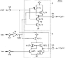
Fig. 2 is the figure of an example of structure of major part that the clock buffer 120 of embodiments of the invention 1 is shown.
Fig. 3 is the circuit diagram of an example of concrete structure that the interface circuit 100 of embodiments of the invention 1 is shown.
Fig. 4 A~Fig. 4 H is the sequential chart of work that is used for the semiconductor memory 1000 of the embodiments of the invention 1 shown in key diagram 1~Fig. 3.
Fig. 5 is the circuit diagram of an example of concrete structure that the interface circuit 200 of embodiment 2 is shown.
Fig. 6 A~Fig. 6 H is the sequential chart that is used for the work of the interface circuit 200.1 shown in the key diagram 5.
Fig. 7 is the circuit diagram of another concrete structure that the interface circuit 200 of embodiment 2 is shown.
Fig. 8 A~Fig. 8 H is the sequential chart that is used for the work of the interface circuit 200.2 shown in the key diagram 7.
Fig. 9 is the circuit diagram of an example of concrete structure that the interface circuit 200 of embodiments of the invention 2 is shown.
Figure 10 A~Figure 10 H is the sequential chart that is used for the work of the interface circuit 200.3 shown in the key diagram 9.
Figure 11 is the schematic block diagram of structure that the major part of conventional semiconductor storer 9000 is shown.
Figure 12 is the circuit diagram of an example that the concrete structure of existing input buffer 1 (LVTTL interface circuit) is shown.
Figure 13 is the circuit diagram of an example that the concrete structure of existing SSTL interface circuit 2 is shown.
[embodiment 1]
The semiconductor memory of embodiments of the invention 1 possesses a plurality of interface circuits, by response and mode of operation and the switching interface circuit can realize transmitting at a high speed and reducing current sinking.
Use Fig. 1 that the semiconductor memory of embodiments of the invention 1 is described.
For example, reading under the mode of operation, the combination by external control signal is arranged at mode register 124 reads mode of operation.Moreover, become selection mode corresponding to the storage unit of external address signal A.And, according to the control of control circuit 123, carry out the reading of canned data of selecteed storage unit.The canned data of the storage unit that is read out is sent to inputoutput buffer 128, and (DQ) outputs to the outside from the data input and output pin.Writing under the mode of operation, after having selected certain storage unit, will be written to the selecteed storage unit from the data DQ of data input and output pin input.
Under self refresh mode,, automatically carry out the renewal of the storage unit that comprises in the memory cell array 126 according to the internal address signal that takes place by self refresh counter 125.Impact damper except that clock buffer 120 (address buffer 121, controller buffer 122 and inputoutput buffer 128) response stops its work respectively corresponding to the internal signal of low level external clock enabling signal ext.CKE.That is, under self refresh mode, become respectively from the input of address pin, control pin and data input and output pin and to forbid the state that receives, just clock buffer 120 is in running order.
Secondly, use Fig. 2 that the interface circuit that comprises in the clock buffer 120 in the embodiments of the invention 1 is described.Clock buffer 120 shown in Fig. 2 comprises interface circuit 100, logical circuit 102 and NOR circuit 104.
Interface circuit 100 comprises 2 kinds of interface circuits as described below.Interface circuit 100 is received from from node N1 and upgrades trigger pip SEL, receives internal signal, is clock enabling signal CKE from node N2, receives reference potential Vref from node N3.Interface circuit 100 response self refresh trigger pip SEL export VOUT1 or VOUT2 corresponding to clock enable signal CKE respectively from node N4 or node N5.
Logical circuit 102 receives VOUT1 or VOUT2, makes the logic level unanimity.NOR circuit 104 receives corresponding to the signal of signal VOUT1 or corresponding to the signal of signal VOUT2, output is corresponding to the internal signal (being OUT in Fig. 2) of clock enable signal CKE from logical circuit 102.
Secondly, use the concrete structure of Fig. 3 specification interface circuit 100.
Interface circuit 100 comprises NOR circuit 1 and differential amplifier 2.
As having illustrated among Figure 12, NOR circuit 1 comprises P channel type MOS transistor PLT1 and PLT2 and N channel type MOS transistor NLT1 and NLT2.
The gate electrode separately of P channel type MOS transistor PLT1 and N channel type MOS transistor NLT2 is received from and upgrades trigger pip SEL.The gate electrode receive clock enabling signal CKE separately of P channel type MOS transistor PLT2 and N channel type MOS transistor NLT1 in addition.
Response clock enable signal CKE, the node N4 output signal VOUT1 that is connected from connected node with P channel type MOS transistor PLT2 and N channel type MOS transistor NLT1.Have, NOR circuit 1 is the LVTTL interface as previously discussed again, the input signal of response LVTTL level, output VOUT1.
As shown in Figure 13, differential amplifier 2 comprises P channel type MOS transistor PST1 and PST2 and N channel type MOS transistor NST1, NST2 and NST3.
The gate electrode of N channel type MOS transistor NST3 is received from and upgrades trigger pip SEL.The gate electrode receive clock enabling signal CKE of N channel type MOS transistor NST2.The gate electrode of N channel type MOS transistor NST1 receives reference potential Vref.Response clock enable signal CKE, the node N5 output signal VOUT2 that is connected from connected node with P channel type MOS transistor PST2 and N channel type MOS transistor NST2.Have, differential amplifier 2 is the SSTL interface as previously discussed again, responds with intermediate potential, is that reference potential Vref is a benchmark oscillatory signal minutely, output VOUT2.
Secondly, use Fig. 4 A~Fig. 4 H, the work of the major part in the semiconductor memory 1000 shown in key diagram 1~Fig. 3 as sequential chart.
Work (the t0~t1) constantly of the semiconductor memory 1000 under the pattern except that self refresh mode at first, is described.At this moment, self refresh trigger pip SEL is in the unactivated state of high level.N channel type MOS transistor NST3 is a conducting state, and the current potential of node Z1 (connected node of N channel type MOS transistor NST1 and N channel type MOS transistor NST2) is in low level.Thereby differential amplifier 2 is in starting state.
On the other hand, P channel type MOS transistor PLT1 is a nonconducting state, N channel type MOS transistor NLT2 is a conducting state, and the current potential of node Y1 (connected node of P channel type MOS transistor PLT1 and P channel type MOS transistor PLT2) is in the state higher slightly than low level.Thus, NOR circuit 1 is in illegal state.
If the clock enable signal CKE of input high level under this state (reference potential Vref+ amplitude VH), then differential amplifier 2 amplify clock enable signals CKE with potential difference (PD) reference potential Vref, output VOUT2.VOUT1 by 1 output of NOR circuit is maintained at low level.
Secondly, the situation of having specified self refresh mode is described.At this moment, corresponding with self refresh mode, low level self refresh trigger pip SEL (moment t1~) takes place.
N channel type MOS transistor NST3 becomes nonconducting state, till the electric current that the current potential of node Z1 rises to P channel type MOS transistor PST1 and N channel type MOS transistor NST1 balances each other.Thus, differential amplifier 2 becomes illegal state.
On the other hand, P channel type MOS transistor PLT1 becomes conducting state, and the current potential of node Y1 rises to power supply potential VDD.Response clock enable signal CKE is from NOR circuit 1 output signal VOUT1.
Have again, more particularly, under self refresh mode, external clock enabling signal ext.CKE is below the 0.2V, owing to be in, in the CMOS phase inverter that constitutes NOR circuit 1, do not flow through punchthrough current than the low voltage level of transistorized threshold voltage that constitutes NOR circuit 1.In addition, because differential amplifier 2 is in illegal state, so do not produce electric current.Thereby, compare as the situation of interface circuit with using differential amplifier 2 individually, can reduce current sinking.
As mentioned above, the semiconductor memory of embodiments of the invention 1 by the switching interface circuit, can reduce current sinking under the pattern that is necessary to suppress current sinking (for example, self refresh mode).
[embodiment 2]
Semiconductor memory about embodiment 2 describes.The one-piece construction of the semiconductor memory of embodiment 2 is identical with the structure of the semiconductor memory 1000 shown in Fig. 1.
The semiconductor memory 1000 of embodiment 2 possesses the following interface circuit that illustrates 200, replaces the interface circuit 100 shown in Fig. 1.Use the circuit diagram of Fig. 5, an example of interface circuit 200 concrete structures of embodiment 2 is described.
For the textural element identical with the interface circuit 100 of the embodiment 1 shown in Fig. 3, attached with identical mark and symbol, omit its explanation.Interface circuit 200 shown in Fig. 5 (hereinafter referred to as interface circuit 200.1) comprises phase inverter I2, NAND circuit 3 and differential amplifier 4.
The self refresh trigger pip SEL counter-rotating back output that phase inverter I2 will receive at node N1 (is called counter-rotating self refresh trigger pip/SEL).
Moreover differential amplifier 4 comprises phase inverter I1.Phase inverter I1 will reverse and export after self refresh trigger pip/SEL reverses.The gate electrode of N channel type MOS transistor NST3 receives and the synchronous signal of self refresh trigger pip SEL by phase inverter I1.Response clock enable signal CKE, the node N5 output signal VOUT2 that is connected from connected node with P channel type MOS transistor PST2 and N channel type MOS transistor NST2.Have, differential amplifier 4 is the SSTL interface as previously discussed again.
The gate electrode receive clock enabling signal CKE separately of P channel type MOS transistor PLT3 and N channel type MOS transistor NLT3.The gate electrode separately of P channel type MOS transistor PLT4 and N channel type MOS transistor NLT4 receives counter-rotating self refresh trigger pip/SEL from phase inverter I2.Response clock enable signal CKE, the node N4 output signal VOUT1 that is connected from connected node with P channel type MOS transistor PST3 and N channel type MOS transistor NST3.Have, NAND circuit 3 is a kind of of LVTTL interface again, and the input signal of response LVTTL level is exported signal VOUT1.
Secondly, use the sequential chart of Fig. 6 A~Fig. 6 H, the work of the interface circuit 200.1 shown in the key diagram 5.
At first, work under the pattern except that self refresh mode (t0~t1) constantly is described.At this moment, self refresh trigger pip SEL is in the unactivated state of high level (counter-rotating self refresh trigger pip/SEL is a low level), N channel type MOS transistor NST3 is a conducting state, and the current potential of node Z1 (connected node of N channel type MOS transistor NLT1 and N channel type MOS transistor NLT2) is in low level.Thus, differential amplifier 4 is in starting state.
On the other hand, N channel type MOS transistor NLT4 is a nonconducting state, P channel type MOS transistor PLT4 is a conducting state, and the current potential of node Y2 (connected node of N channel type MOS transistor NLT3 and N channel type MOS transistor NLT4) is in the state higher slightly than low level.Thus, NAND circuit 3 is in illegal state.
If the clock enable signal CKE of input high level under this state (reference potential Vref+ amplitude VH), then differential amplifier 4 amplify clock enable signals CKE with potential difference (PD) reference potential Vref, output signal VOUT2.VOUT1 by 3 outputs of NAND circuit is maintained at low level.
Secondly, the situation of having specified self refresh mode is described.At this moment, corresponding with self refresh mode, low level self refresh trigger pip SEL (moment t1~) takes place.
N channel type MOS transistor NST3 becomes nonconducting state, till the electric current that the current potential of node Z1 rises to P channel type MOS transistor PST1 and N channel type MOS transistor NST1 balances each other.Thus, differential amplifier 4 becomes illegal state.
On the other hand, N channel type MOS transistor NLT4 becomes conducting state, and P channel type MOS transistor PLT4 becomes nonconducting state, and the current potential of node Y2 drops to low level.Thus, NAND circuit 3 becomes starting state.Response is as the clock enable signal CKE of internal signal, from NAND circuit 3 output signal VOUT1.
As mentioned above, more particularly, under self refresh mode, external clock enabling signal ext.CKE is below the 0.2V, owing to be in, in the CMOS phase inverter that constitutes NAND circuit 3, do not flow through punchthrough current than the low potential level of transistorized threshold voltage that constitutes NAND circuit 3.In addition, because differential amplifier 4 is in illegal state, so do not produce electric current.Thereby, compare as the situation of interface circuit with using differential amplifier 4 individually, can reduce current sinking.
Secondly, use Fig. 7 that other a example of concrete structure of the interface circuit 200 of embodiments of the invention 2 is described.
For the textural element identical with the interface circuit 100 shown in Fig. 3, attached with identical symbol and mark, omit its explanation.
Interface circuit 200 shown in Fig. 7 (hereinafter referred to as interface circuit 200.2) comprises NOR circuit 1 and differential amplifier 5.As mentioned above, NOR circuit 1 is the LVTTL interface, and response self refresh trigger pip SEL exports the signal VOUT1 corresponding with clock enable signal CKE.
Differential amplifier 5 comprises P channel type MOS transistor PST1 and PST2 and N channel type MOS transistor NST1 and NST2.About the annexation of P channel type MOS transistor PST1 and PST2, N channel type MOS transistor NST1 and NST2, identical with the structure of differential amplifier 2 among Fig. 3.
Differential amplifier 5 also comprises phase inverter I3 and P channel type MOS transistor PST3.Phase inverter I3 is with self refresh trigger pip SEL counter-rotating back output.
P channel type MOS transistor PST3 is connected between the Lead-through terminal separately of power supply potential VDD and P channel type MOS transistor PST1 and PST2.P channel type MOS transistor PST3 is an oxide-semiconductor control transistors, and its gate electrode is by phase inverter I3, receives the signal after the self refresh trigger pip SEL counter-rotating (is called counter-rotating self refresh trigger pip/SEL).The conduction/non-conduction state of differential amplifier 5 response P channel type MOS transistor PST3 becomes startup/illegal state.Have, differential amplifier 5 is SSTL interfaces again.
Secondly, use the sequential chart of Fig. 8 A~Fig. 8 H, the work of the interface circuit 200.2 shown in the key diagram 7.
At first, work under the pattern except that self refresh mode (t0~t1) constantly is described.At this moment, self refresh trigger pip SEL is in the unactivated state of high level (counter-rotating self refresh trigger pip/SEL is a low level), P channel type MOS transistor PST3 is a conducting state, and node Z1 (connected node of N channel type MOS transistor NST1 and N channel type MOS transistor NST2) is in low level state.Thus, differential amplifier 5 is in starting state.
On the other hand, N channel type MOS transistor NLT2 is a conducting state, P channel type MOS transistor PLT1 is a nonconducting state, and the current potential of node Y1 (connected node of P channel type MOS transistor PLT1 and P channel type MOS transistor PLT2) is in the state higher slightly than low level.Thus, NOR circuit 1 is in illegal state.
If the clock enable signal CKE of input high level under this state (reference potential Vref+ amplitude VH), then differential amplifier 5 amplify clock enable signals CKE with potential difference (PD) reference potential Vref, output signal VOUT2.VOUT1 by 1 output of NOR circuit is maintained at low level.
Secondly, the situation of having specified self refresh mode is described.At this moment, corresponding with self refresh mode, low level self refresh trigger pip SEL (moment t1~) takes place.
P channel type MOS transistor PST3 becomes nonconducting state, and differential amplifier 5 becomes illegal state.
On the other hand, P channel type MOS transistor PLT1 becomes conducting state, and the current potential of node Y1 rises to power supply potential VDD.Thus, NOR circuit 1 becomes starting state.Response clock enable signal CKE is from NOR circuit 1 output signal VOUT1.
As mentioned above, more particularly, under self refresh mode, external clock enabling signal ext.CKE is below the 0.2V, owing to be in, in the CMOS phase inverter that constitutes NOR circuit 1, do not flow through punchthrough current than the low voltage level of transistorized threshold voltage that constitutes NOR circuit 1.In addition, because differential amplifier 5 is in illegal state, so do not produce electric current.Thereby, compare as the situation of interface circuit with using differential amplifier 5 individually, can reduce current sinking.
Secondly, use Fig. 9 that other a example of concrete structure of the interface circuit 200 of embodiments of the invention 2 is described.
For with interface circuit 100 shown in Fig. 3, Fig. 5 and Fig. 7 and 200 identical textural elements, attached with identical symbol and mark, omit its explanation.Interface circuit 200 shown in Fig. 9 (hereinafter referred to as interface circuit 200.3) comprises phase inverter I4, NAND circuit 3 and differential amplifier 6.
The self refresh trigger pip SEL counter-rotating back output that phase inverter I4 will receive at node N1 (is called counter-rotating self refresh trigger pip/SEL).
P channel type MOS transistor PST3 is an oxide-semiconductor control transistors, and the gate electrode of P channel type MOS transistor PST3 receives counter-rotating self refresh trigger pip/SEL by phase inverter I4.The conduction/non-conduction state of differential amplifier 6 response P channel type MOS transistor PST3 becomes startup/illegal state.Have, differential amplifier 6 is SSTL interfaces again.
Respectively by phase inverter I4, receive counter-rotating self refresh trigger pip/SEL as the gate electrode of the P channel type MOS transistor PLT4 of the oxide-semiconductor control transistors of NAND circuit 3 and N channel type MOS transistor NLT4.As mentioned above, NAND circuit 3 is a kind of of LVTTL interface, response self refresh trigger pip SEL, and output is corresponding to the signal VOUT1 of clock enable signal CKE.
Secondly, use the sequential chart of Figure 10 A~Figure 10 H, the work of the interface circuit 200.3 shown in the key diagram 9.
At first, work under the pattern except that self refresh mode (t0~t1) constantly is described.At this moment, self refresh trigger pip SEL is in the unactivated state of high level (counter-rotating self refresh trigger pip/SEL is a low level), P channel type MOS transistor PST3 is a conducting state, and node Z1 (connected node of N channel type MOS transistor NST1 and N channel type MOS transistor NST2) is in low level state.Thus, differential amplifier 6 is in starting state.
On the other hand, N channel type MOS transistor NLT4 is a nonconducting state, P channel type MOS transistor PLT4 is a conducting state, and the current potential of node Y2 (connected node of N channel type MOS transistor NLT3 and N channel type MOS transistor NLT4) is in the state higher slightly than low level.Thus, NAND circuit 3 is in illegal state.
If the clock enable signal CKE of input high level under this state (reference potential Vref+ amplitude VH), then differential amplifier 6 amplify clock enable signals CKE with potential difference (PD) reference potential Vref, output signal VOUT2.VOUT1 by 3 outputs of NAND circuit is maintained at low level.
Secondly, the situation of having specified self refresh mode is described.At this moment, corresponding with self refresh mode, low level self refresh trigger pip SEL (moment t1~) takes place.
P channel type MOS transistor PST3 becomes nonconducting state, and differential amplifier 6 becomes illegal state.
On the other hand, N channel type MOS transistor NLT4 becomes conducting state, and the current potential of node Y2 drops to low level.Thus, NAND circuit 3 becomes starting state.Response clock enable signal CKE is from NAND circuit 3 output signal VOUT1.
As mentioned above, more particularly, under self refresh mode, external clock enabling signal ext.CKE is below the 0.2V, owing to be in, in the CMOS phase inverter that constitutes NAND circuit 3, do not flow through punchthrough current than the low voltage level of transistorized threshold voltage that constitutes NAND circuit 3.In addition, because differential amplifier 6 is in illegal state, so do not produce electric current.Thereby, compare as the situation of interface circuit with using differential amplifier 6 individually, can reduce current sinking.
As mentioned above, in the semiconductor memory of embodiments of the invention 2, under the pattern that is necessary to suppress current sinking (for example, self refresh mode),, also can reduce current sinking by the switching interface circuit.
Claims (15)
1. semiconductor memory is characterized in that:
Possess:
Mode register (124), this mode register response detects the appointed situation of specific pattern from the mode designating signal of outside input, as the corresponding pattern trigger pip of testing result output;
The input terminal of the input signal that reception sends from the outside, the input signal that sends from the outside is under above-mentioned specific pattern, being the signal of the 1st potential level, under the pattern except that above-mentioned specific pattern, is the overlapping signal of little amplitude logical signal on the 2nd potential level; And
The internal circuit that responds input signal and work,
Also possess:
The 1st interface arrangement (1,3) and the 2nd interface arrangement (2,4), wherein, the 1st interface arrangement activates under above-mentioned specific pattern, according to comparison from the potential level of the potential level of the above-mentioned input signal of above-mentioned input terminal input and threshold value, judge above-mentioned logical level of input signals, to output to above-mentioned internal circuit corresponding to the internal signal of result of determination, the 2nd interface arrangement activates under the pattern except that above-mentioned specific pattern, according to the potential level of the above-mentioned input signal of importing from above-mentioned input terminal and the comparison of above-mentioned the 2nd potential level, judge above-mentioned logical level of input signals, will output to above-mentioned internal circuit corresponding to the internal signal of result of determination.
2. the semiconductor memory described in claim 1 is characterized in that:
Also comprise:
Memory cell array (126) comprises a plurality of storage unit that are configured to the ranks shape; And
Address producing device (125) responds the testing result of above-mentioned mode register, produces the internal address signal of the said memory cells of specifying the said memory cells array,
So-called above-mentioned AD HOC is the above-mentioned internal address signal that the above-mentioned address producing device of response (125) produces, with the self refresh mode of the Data Update of said memory cells.
3. the semiconductor memory described in claim 2 is characterized in that:
Above-mentioned the 1st interface arrangement (1) is made of the NOR circuit.
4. the semiconductor memory described in claim 2 is characterized in that:
Above-mentioned the 1st interface arrangement is made of NAND circuit (3).
5. the semiconductor memory described in claim 2 is characterized in that:
Above-mentioned the 2nd interface arrangement (2,4) is made of the differential amplifier of the potential difference (PD) of amplifying above-mentioned the 2nd potential level and above-mentioned input signal.
6. the semiconductor memory described in claim 3 is characterized in that:
Above-mentioned pattern trigger pip becomes low level state of activation under above-mentioned self refresh mode,
Above-mentioned the 1st interface arrangement (1) comprising:
The 1st P channel type MOS transistor (PLT1), an one Lead-through terminal is connected to power supply potential;
The 2nd P channel type MOS transistor (PLT2), an one Lead-through terminal is connected with another Lead-through terminal of above-mentioned the 1st P channel type MOS transistor (PLT1); And
The 1st N channel type MOS transistor (NLT1) and the 2nd N channel type MOS transistor (NLT2) are connected between another Lead-through terminal and earthing potential of above-mentioned the 2nd P channel type MOS transistor (PLT2) in parallel,
The gate electrode separately of above-mentioned the 1st P channel type MOS transistor (PLT1) and above-mentioned the 2nd N channel type MOS transistor (NLT2) receives above-mentioned pattern trigger pip,
The gate electrode separately of above-mentioned the 2nd P channel type MOS transistor (PLT2) and above-mentioned the 1st N channel type MOS transistor (NLT1) receives above-mentioned input signal,
Export above-mentioned internal signal from above-mentioned the 2nd P channel type MOS transistor (PLT2) and the connected node of above-mentioned the 1st N channel type MOS transistor (NLT1).
7. the semiconductor memory described in claim 4 is characterized in that:
Above-mentioned pattern trigger pip becomes low level state of activation under above-mentioned self refresh mode,
Above-mentioned the 1st interface arrangement (3) comprising:
The 1st P channel type MOS transistor (PLT3) and the 2nd P channel type MOS transistor (PLT4), an one Lead-through terminal is connected respectively to power supply potential; And
The 1st N channel type MOS transistor (NLT3) and the 2nd N channel type MOS transistor (NLT4), be connected in series between separately another Lead-through terminal and earthing potential of above-mentioned the 1st P channel type MOS transistor (PLT3) and the 2nd P channel type MOS transistor (PLT4)
The gate electrode separately of above-mentioned the 2nd P channel type MOS transistor (PLT4) and above-mentioned the 2nd N channel type MOS transistor (NLT4) receives the signal after the above-mentioned pattern trigger pip counter-rotating,
The gate electrode separately of above-mentioned the 1st P channel type MOS transistor (PLT3) and above-mentioned the 1st N channel type MOS transistor (NLT3) receives above-mentioned input signal,
Export above-mentioned internal signal from above-mentioned the 1st P channel type MOS transistor (PLT3) and the connected node of above-mentioned the 1st N channel type MOS transistor (NLT3).
8. the semiconductor memory described in claim 5 is characterized in that:
Above-mentioned pattern trigger pip becomes low level state of activation under above-mentioned self refresh mode,
Above-mentioned the 2nd interface arrangement (2) comprising:
The 1st P channel type MOS transistor (PST1) and the 2nd P channel type MOS transistor (PST2), its Lead-through terminal separately is connected respectively to power supply potential;
The 1st N channel type MOS transistor (NST1), an one Lead-through terminal is connected with another Lead-through terminal of above-mentioned the 1st P channel type MOS transistor (PST1);
The 2nd N channel type MOS transistor (NST2), an one Lead-through terminal is connected with another Lead-through terminal of above-mentioned the 2nd P channel type MOS transistor (PST2);
And
The 3rd N channel type MOS transistor (NST3) is connected between separately another Lead-through terminal and earthing potential of above-mentioned the 1st N channel type MOS transistor (NST1) and the 2nd N channel type MOS transistor (NST2),
The gate electrode separately of above-mentioned the 1st P channel type MOS transistor (PST1) and above-mentioned the 2nd P channel type MOS transistor (PST2) is connected to the connected node of above-mentioned the 1st P channel type MOS transistor (PST1) and above-mentioned the 1st N channel type MOS transistor (NST1)
The gate electrode of above-mentioned the 3rd N channel type MOS transistor (NST3) receives above-mentioned pattern trigger pip,
The gate electrode of above-mentioned the 1st N channel type MOS transistor (NST1) receives the reference potential of above-mentioned the 2nd potential level,
The gate electrode of above-mentioned the 2nd N channel type MOS transistor (NST2) receives above-mentioned input signal,
Export above-mentioned internal signal from above-mentioned the 2nd P channel type MOS transistor (PST2) and the connected node of above-mentioned the 2nd N channel type MOS transistor (NST2).
9. the semiconductor memory described in claim 5 is characterized in that:
Above-mentioned pattern trigger pip becomes low level state of activation under above-mentioned self refresh mode,
Above-mentioned the 2nd interface arrangement (4) comprising:
The 1st P channel type MOS transistor (PST1) and the 2nd P channel type MOS transistor (PST2) couple together separately a Lead-through terminal;
The 1st N channel type MOS transistor (NST1) is connected between another Lead-through terminal and earthing potential of above-mentioned the 1st P channel type MOS transistor (PST1);
The 2nd N channel type MOS transistor (NST2) is connected between another Lead-through terminal and earthing potential of above-mentioned the 2nd P channel type MOS transistor (PST2);
And
The 3rd P channel type MOS transistor (PST3) is connected between separately another Lead-through terminal and power supply potential of above-mentioned the 1st P channel type MOS transistor (PST1) and above-mentioned the 2nd P channel type MOS transistor (PST2),
The gate electrode separately of above-mentioned the 1st P channel type MOS transistor (PST1) and above-mentioned the 2nd P channel type MOS transistor (PST2) is connected to the connected node of above-mentioned the 1st P channel type MOS transistor (PST1) and above-mentioned the 1st N channel type MOS transistor (NST1)
The gate electrode of above-mentioned the 3rd P channel type MOS transistor (PST3) receives the signal after the above-mentioned pattern trigger pip counter-rotating,
The gate electrode of above-mentioned the 1st N channel type MOS transistor (NST1) receives the reference potential of above-mentioned the 2nd potential level,
The gate electrode of above-mentioned the 2nd N channel type MOS transistor (NST2) receives above-mentioned input signal,
Export above-mentioned internal signal from above-mentioned the 2nd P channel type MOS transistor (PST2) and the connected node of above-mentioned the 2nd N channel type MOS transistor (NST2).
10. the semiconductor memory described in claim 2 is characterized in that:
Above-mentioned pattern trigger pip becomes low level state of activation under above-mentioned self refresh mode,
Above-mentioned the 1st interface arrangement (1) comprising:
The 1st P channel type MOS transistor (PLT1), an one Lead-through terminal is connected to power supply potential;
The 2nd P channel type MOS transistor (PLT2), an one Lead-through terminal is connected with another Lead-through terminal of above-mentioned the 1st P channel type MOS transistor (PLT1); And
The 1st N channel type MOS transistor (NLT1) and the 2nd N channel type MOS transistor (NLT2) are connected between another Lead-through terminal and earthing potential of above-mentioned the 2nd P channel type MOS transistor (PLT2) in parallel,
The gate electrode separately of above-mentioned the 1st P channel type MOS transistor (PLT1) and above-mentioned the 2nd N channel type MOS transistor (NLT2) receives above-mentioned pattern trigger pip,
The gate electrode separately of above-mentioned the 2nd P channel type MOS transistor (PLT2) and above-mentioned the 1st N channel type MOS transistor (NLT1) receives above-mentioned input signal,
Export above-mentioned internal signal from above-mentioned the 2nd P channel type MOS transistor (PLT2) and the connected node of above-mentioned the 1st N channel type MOS transistor (NLT1),
Above-mentioned the 2nd interface arrangement (2) comprising:
The 3rd P channel type MOS transistor (PST1) and the 4th P channel type MOS transistor (PST2), its Lead-through terminal separately is connected respectively to power supply potential;
The 3rd N channel type MOS transistor (NST1), an one Lead-through terminal is connected with another Lead-through terminal of above-mentioned the 3rd P channel type MOS transistor (PST1);
The 4th N channel type MOS transistor (NST2), an one Lead-through terminal is connected with another Lead-through terminal of above-mentioned the 4th P channel type MOS transistor (PST2);
And
The 5th N channel type MOS transistor (NST3) is connected between separately another Lead-through terminal and earthing potential of above-mentioned the 3rd N channel type MOS transistor (NST1) and the 4th N channel type MOS transistor (NST2),
The gate electrode separately of above-mentioned the 3rd P channel type MOS transistor (PST1) and above-mentioned the 4th P channel type MOS transistor (PST2) is connected to the connected node of above-mentioned the 3rd P channel type MOS transistor (PST1) and above-mentioned the 3rd N channel type MOS transistor (NST1)
The gate electrode of above-mentioned the 5th N channel type MOS transistor (NST3) receives above-mentioned pattern trigger pip,
The gate electrode of above-mentioned the 3rd N channel type MOS transistor (NST1) receives the reference potential of above-mentioned the 2nd potential level,
The gate electrode of above-mentioned the 4th N channel type MOS transistor (NST2) receives above-mentioned input signal,
Export above-mentioned internal signal from above-mentioned the 4th P channel type MOS transistor (PST2) and the connected node of above-mentioned the 4th N channel type MOS transistor (NST2).
11. the semiconductor memory described in claim 2 is characterized in that:
Above-mentioned pattern trigger pip becomes low level state of activation under above-mentioned self refresh mode,
Above-mentioned the 1st interface arrangement (3) comprising:
The 1st P channel type MOS transistor (PLT3) and the 2nd P channel type MOS transistor (PLT4), an one Lead-through terminal is connected respectively to power supply potential; And
The 1st N channel type MOS transistor (NLT3) and the 2nd N channel type MOS transistor (NLT4), be connected in series between separately another Lead-through terminal and earthing potential of above-mentioned the 1st P channel type MOS transistor (PLT3) and the 2nd P channel type MOS transistor (PLT4)
The gate electrode separately of above-mentioned the 2nd P channel type MOS transistor (PLT4) and above-mentioned the 2nd N channel type MOS transistor (NLT4) receives the signal after the above-mentioned pattern trigger pip counter-rotating,
The gate electrode separately of above-mentioned the 1st P channel type MOS transistor (PLT3) and above-mentioned the 1st N channel type MOS transistor (NLT3) receives above-mentioned input signal,
Export above-mentioned internal signal from above-mentioned the 1st P channel type MOS transistor (PLT3) and the connected node of above-mentioned the 1st N channel type MOS transistor (NLT3),
Above-mentioned the 2nd interface arrangement (2) comprising:
The 3rd P channel type MOS transistor (PST1) and the 4th P channel type MOS transistor (PST2), its Lead-through terminal separately is connected respectively to power supply potential;
The 3rd N channel type MOS transistor (NST1), an one Lead-through terminal is connected with another Lead-through terminal of above-mentioned the 3rd P channel type MOS transistor (PST1);
The 4th N channel type MOS transistor (NST2), an one Lead-through terminal is connected with another Lead-through terminal of above-mentioned the 4th P channel type MOS transistor (PST2);
And
The 5th N channel type MOS transistor (NST3) is connected between separately another Lead-through terminal and earthing potential of above-mentioned the 3rd N channel type MOS transistor (NST1) and the 4th N channel type MOS transistor (NST2),
The gate electrode separately of above-mentioned the 3rd P channel type MOS transistor (PST1) and above-mentioned the 4th P channel type MOS transistor (PST2) is connected to the connected node of above-mentioned the 3rd P channel type MOS transistor (PST1) and above-mentioned the 3rd N channel type MOS transistor (NST1)
The gate electrode of above-mentioned the 5th N channel type MOS transistor (NST3) receives above-mentioned pattern trigger pip,
The gate electrode of above-mentioned the 3rd N channel type MOS transistor (NST1) receives the reference potential of above-mentioned the 2nd potential level,
The gate electrode of above-mentioned the 4th N channel type MOS transistor (NST2) receives above-mentioned input signal,
Export above-mentioned internal signal from above-mentioned the 4th P channel type MOS transistor (PST2) and the connected node of above-mentioned the 4th N channel type MOS transistor (NST2).
12. the semiconductor memory described in claim 2 is characterized in that:
Above-mentioned pattern trigger pip becomes low level state of activation under above-mentioned self refresh mode,
Above-mentioned the 1st interface arrangement (1) comprising:
The 1st P channel type MOS transistor (PLT1), an one Lead-through terminal is connected to power supply potential;
The 2nd P channel type MOS transistor (PLT2), an one Lead-through terminal is connected with another Lead-through terminal of above-mentioned the 1st P channel type MOS transistor (PLT1); And
The 1st N channel type MOS transistor (NLT1) and the 2nd N channel type MOS transistor (NLT2) are connected between another Lead-through terminal and earthing potential of above-mentioned the 2nd P channel type MOS transistor (PLT2) in parallel,
The gate electrode separately of above-mentioned the 1st P channel type MOS transistor (PLT1) and above-mentioned the 2nd N channel type MOS transistor (NLT2) receives above-mentioned pattern trigger pip,
The gate electrode separately of above-mentioned the 2nd P channel type MOS transistor (PLT2) and above-mentioned the 1st N channel type MOS transistor (NLT1) receives above-mentioned input signal,
Export above-mentioned internal signal from above-mentioned the 2nd P channel type MOS transistor (PLT2) and the connected node of above-mentioned the 1st N channel type MOS transistor (NLT1),
Above-mentioned the 2nd interface arrangement (4) comprising:
The 3rd P channel type MOS transistor (PST1) and the 4th P channel type MOS transistor (PST2) couple together separately a Lead-through terminal;
The 3rd N channel type MOS transistor (NST1) is connected between another Lead-through terminal and earthing potential of above-mentioned the 3rd P channel type MOS transistor (PST1);
The 4th N channel type MOS transistor (NST2) is connected between another Lead-through terminal and earthing potential of above-mentioned the 4th P channel type MOS transistor (PST2);
And
The 5th P channel type MOS transistor (PST3) is connected between separately another Lead-through terminal and power supply potential of above-mentioned the 3rd P channel type MOS transistor (PST1) and above-mentioned the 4th P channel type MOS transistor (PST2),
The gate electrode separately of above-mentioned the 3rd P channel type MOS transistor (PST1) and above-mentioned the 4th P channel type MOS transistor (PST2) is connected to the connected node of above-mentioned the 3rd P channel type MOS transistor (PST1) and above-mentioned the 3rd N channel type MOS transistor (NST1)
The gate electrode of above-mentioned the 5th P channel type MOS transistor (PST3) receives the signal after the above-mentioned pattern trigger pip counter-rotating,
The gate electrode of above-mentioned the 3rd N channel type MOS transistor (NST1) receives the reference potential of above-mentioned the 2nd potential level,
The gate electrode of above-mentioned the 4th N channel type MOS transistor (NST2) receives above-mentioned input signal,
Export above-mentioned internal signal from above-mentioned the 4th P channel type MOS transistor (PST2) and the connected node of above-mentioned the 4th N channel type MOS transistor (NST2).
13. the semiconductor memory described in claim 2 is characterized in that:
Above-mentioned pattern trigger pip becomes low level state of activation under above-mentioned self refresh mode,
Above-mentioned the 1st interface arrangement (3) comprising:
The 1st P channel type MOS transistor (PLT3) and the 2nd P channel type MOS transistor (PLT4), an one Lead-through terminal is connected respectively to power supply potential; And
The 1st N channel type MOS transistor (NLT3) and the 2nd N channel type MOS transistor (NLT4), be connected in series between separately another Lead-through terminal and earthing potential of above-mentioned the 1st P channel type MOS transistor (PLT3) and the 2nd P channel type MOS transistor (PLT4)
The gate electrode separately of above-mentioned the 2nd P channel type MOS transistor (PLT4) and above-mentioned the 2nd N channel type MOS transistor (NLT4) receives the signal after the above-mentioned pattern trigger pip counter-rotating,
The gate electrode separately of above-mentioned the 1st P channel type MOS transistor (PLT3) and above-mentioned the 1st N channel type MOS transistor (NLT3) receives above-mentioned input signal,
Export above-mentioned internal signal from above-mentioned the 1st P channel type MOS transistor (PLT3) and the connected node of above-mentioned the 1st N channel type MOS transistor (NLT3),
Above-mentioned the 2nd interface arrangement (4) comprising:
The 3rd P channel type MOS transistor (PST1) and the 4th P channel type MOS transistor (PST2) couple together separately a Lead-through terminal;
The 3rd N channel type MOS transistor (NST1) is connected between another Lead-through terminal and earthing potential of above-mentioned the 3rd P channel type MOS transistor (PST1);
The 4th N channel type MOS transistor (NST2) is connected between another Lead-through terminal and earthing potential of above-mentioned the 4th P channel type MOS transistor (PST2);
And
The 5th P channel type MOS transistor (PST3) is connected between separately another Lead-through terminal and power supply potential of above-mentioned the 3rd P channel type MOS transistor (PST1) and above-mentioned the 4th P channel type MOS transistor (PST2),
The gate electrode separately of above-mentioned the 3rd P channel type MOS transistor (PST1) and above-mentioned the 4th P channel type MOS transistor (PST2) is connected to the connected node of above-mentioned the 3rd P channel type MOS transistor (PST1) and above-mentioned the 3rd N channel type MOS transistor (NST1)
The gate electrode of above-mentioned the 5th P channel type MOS transistor (PST3) receives the signal after the above-mentioned pattern trigger pip counter-rotating,
The gate electrode of above-mentioned the 3rd N channel type MOS transistor (NST1) receives the reference potential of above-mentioned the 2nd potential level,
The gate electrode of above-mentioned the 4th N channel type MOS transistor (NST2) receives above-mentioned input signal,
Export above-mentioned internal signal from above-mentioned the 4th P channel type MOS transistor (PST2) and the connected node of above-mentioned the 4th N channel type MOS transistor (NST2).
14. the semiconductor memory described in claim 1 is characterized in that:
Above-mentioned pattern trigger pip becomes low level state of activation under above-mentioned self refresh mode,
Above-mentioned the 1st interface arrangement (1) comprising:
The 1st P channel type MOS transistor (PLT1), an one Lead-through terminal is connected to power supply potential;
The 2nd P channel type MOS transistor (PLT2), an one Lead-through terminal is connected with another Lead-through terminal of above-mentioned the 1st P channel type MOS transistor (PLT1); And
The 1st N channel type MOS transistor (NLT1) and the 2nd N channel type MOS transistor (NLT2) are connected between another Lead-through terminal and earthing potential of above-mentioned the 2nd P channel type MOS transistor (PLT2) in parallel,
The gate electrode separately of above-mentioned the 1st P channel type MOS transistor (PLT1) and above-mentioned the 2nd N channel type MOS transistor (NLT2) receives above-mentioned pattern trigger pip,
The gate electrode separately of above-mentioned the 2nd P channel type MOS transistor (PLT2) and above-mentioned the 1st N channel type MOS transistor (NLT1) receives above-mentioned input signal,
Export above-mentioned internal signal from above-mentioned the 2nd P channel type MOS transistor (PLT2) and the connected node of above-mentioned the 1st N channel type MOS transistor (NLT1),
Above-mentioned the 2nd interface arrangement (2) comprising:
The 3rd P channel type MOS transistor (PST1) and the 4th P channel type MOS transistor (PST2), its Lead-through terminal separately is connected respectively to power supply potential;
The 3rd N channel type MOS transistor (NST1), an one Lead-through terminal is connected with another Lead-through terminal of above-mentioned the 3rd P channel type MOS transistor (PST1);
The 4th N channel type MOS transistor (NST2), an one Lead-through terminal is connected with another Lead-through terminal of above-mentioned the 4th P channel type MOS transistor (PST2);
And
The 5th N channel type MOS transistor (NST3) is connected between separately another Lead-through terminal and earthing potential of above-mentioned the 3rd N channel type MOS transistor (NST1) and the 4th N channel type MOS transistor (NST2),
The gate electrode separately of above-mentioned the 3rd P channel type MOS transistor (PST1) and above-mentioned the 4th P channel type MOS transistor (PST2) is connected to the connected node of above-mentioned the 3rd P channel type MOS transistor (PST1) and above-mentioned the 3rd N channel type MOS transistor (NST1)
The gate electrode of above-mentioned the 5th N channel type MOS transistor (NST3) receives above-mentioned pattern trigger pip,
The gate electrode of above-mentioned the 3rd N channel type MOS transistor (NST1) receives the reference potential of above-mentioned the 2nd potential level,
The gate electrode of above-mentioned the 4th N channel type MOS transistor (NST2) receives above-mentioned input signal,
Export above-mentioned internal signal from above-mentioned the 4th P channel type MOS transistor (PST2) and the connected node of above-mentioned the 4th N channel type MOS transistor (NST2).
15. the semiconductor memory described in claim 1 is characterized in that:
Above-mentioned pattern trigger pip becomes low level state of activation under above-mentioned specific pattern,
Above-mentioned the 1st interface arrangement (3) comprising:
The 1st P channel type MOS transistor (PLT3) and the 2nd P channel type MOS transistor (PLT4), an one Lead-through terminal is connected respectively to power supply potential; And
The 1st N channel type MOS transistor (NLT3) and the 2nd N channel type MOS transistor (NLT4), be connected in series between separately another Lead-through terminal and earthing potential of above-mentioned the 1st P channel type MOS transistor (PLT3) and the 2nd P channel type MOS transistor (PLT4)
The gate electrode separately of above-mentioned the 2nd P channel type MOS transistor (PLT4) and above-mentioned the 2nd N channel type MOS transistor (NLT4) receives the signal after the above-mentioned pattern trigger pip counter-rotating,
The gate electrode separately of above-mentioned the 1st P channel type MOS transistor (PLT3) and above-mentioned the 1st N channel type MOS transistor (NLT3) receives above-mentioned input signal,
Export above-mentioned internal signal from above-mentioned the 1st P channel type MOS transistor (PLT3) and the connected node of above-mentioned the 1st N channel type MOS transistor (NLT3),
Above-mentioned the 2nd interface arrangement (4) comprising:
The 3rd P channel type MOS transistor (PST1) and the 4th P channel type MOS transistor (PST2) couple together separately a Lead-through terminal;
The 3rd N channel type MOS transistor (NST1) is connected between another Lead-through terminal and earthing potential of above-mentioned the 3rd P channel type MOS transistor (PST1);
The 4th N channel type MOS transistor (NST2) is connected between another Lead-through terminal and earthing potential of above-mentioned the 4th P channel type MOS transistor (PST2);
And
The 5th P channel type MOS transistor (PST3) is connected between separately another Lead-through terminal and power supply potential of above-mentioned the 3rd P channel type MOS transistor (PST1) and above-mentioned the 4th P channel type MOS transistor (PST2),
The gate electrode separately of above-mentioned the 3rd P channel type MOS transistor (PST1) and above-mentioned the 4th P channel type MOS transistor (PST2) is connected to the connected node of above-mentioned the 3rd P channel type MOS transistor (PST1) and above-mentioned the 3rd N channel type MOS transistor (NST1)
The gate electrode of above-mentioned the 5th P channel type MOS transistor (PST3) receives the signal after the above-mentioned pattern trigger pip counter-rotating,
The gate electrode of above-mentioned the 3rd N channel type MOS transistor (NST1) receives the reference potential of above-mentioned the 2nd potential level,
The gate electrode of above-mentioned the 4th N channel type MOS transistor (NST2) receives above-mentioned input signal,
Export above-mentioned internal signal from above-mentioned the 4th P channel type MOS transistor (PST2) and the connected node of above-mentioned the 4th N channel type MOS transistor (NST2).
Applications Claiming Priority (3)
| Application Number | Priority Date | Filing Date | Title |
|---|---|---|---|
| JP10006499A JPH11203866A (en) | 1998-01-16 | 1998-01-16 | Semiconductor storage device |
| JP6499/1998 | 1998-01-16 | ||
| JP6499/98 | 1998-01-16 |
Publications (2)
| Publication Number | Publication Date |
|---|---|
| CN1223442A CN1223442A (en) | 1999-07-21 |
| CN1169156C true CN1169156C (en) | 2004-09-29 |
Family
ID=11640149
Family Applications (1)
| Application Number | Title | Priority Date | Filing Date |
|---|---|---|---|
| CNB98119270XA Expired - Fee Related CN1169156C (en) | 1998-01-16 | 1998-09-15 | Semiconductor memory device provide with interface circuit consuming reduced amount of current consumption |
Country Status (5)
| Country | Link |
|---|---|
| US (1) | US6031782A (en) |
| JP (1) | JPH11203866A (en) |
| KR (1) | KR100306859B1 (en) |
| CN (1) | CN1169156C (en) |
| TW (1) | TW409461B (en) |
Cited By (1)
| Publication number | Priority date | Publication date | Assignee | Title |
|---|---|---|---|---|
| CN104052437A (en) * | 2013-03-14 | 2014-09-17 | 美国亚德诺半导体公司 | Fine timing adjustment method |
Families Citing this family (17)
| Publication number | Priority date | Publication date | Assignee | Title |
|---|---|---|---|---|
| US6347379B1 (en) * | 1998-09-25 | 2002-02-12 | Intel Corporation | Reducing power consumption of an electronic device |
| US6330635B1 (en) * | 1999-04-16 | 2001-12-11 | Intel Corporation | Multiple user interfaces for an integrated flash device |
| TW522399B (en) * | 1999-12-08 | 2003-03-01 | Hitachi Ltd | Semiconductor device |
| KR100443907B1 (en) * | 2001-09-07 | 2004-08-09 | 삼성전자주식회사 | Address buffer and semiconductor memory device using this buffer |
| US6771553B2 (en) * | 2001-10-18 | 2004-08-03 | Micron Technology, Inc. | Low power auto-refresh circuit and method for dynamic random access memories |
| US6976181B2 (en) * | 2001-12-20 | 2005-12-13 | Intel Corporation | Method and apparatus for enabling a low power mode for a processor |
| JP3667700B2 (en) | 2002-03-06 | 2005-07-06 | エルピーダメモリ株式会社 | Input buffer circuit and semiconductor memory device |
| US6731548B2 (en) * | 2002-06-07 | 2004-05-04 | Micron Technology, Inc. | Reduced power registered memory module and method |
| KR100506929B1 (en) * | 2002-08-08 | 2005-08-09 | 삼성전자주식회사 | Input buffer of a synchronous semiconductor memory device |
| KR100502664B1 (en) | 2003-04-29 | 2005-07-20 | 주식회사 하이닉스반도체 | On Die Termination Mode Conversion Circuit and its Method |
| JP4592281B2 (en) * | 2003-12-18 | 2010-12-01 | ルネサスエレクトロニクス株式会社 | LSI interface circuit |
| KR100571651B1 (en) * | 2003-12-29 | 2006-04-17 | 주식회사 하이닉스반도체 | Control circuit for escaping power-down mode confidentially |
| US7545194B2 (en) * | 2006-06-30 | 2009-06-09 | Intel Corporation | Programmable delay for clock phase error correction |
| KR100914074B1 (en) | 2007-10-09 | 2009-08-28 | 창원대학교 산학협력단 | Receiver for implementing high speed signal transmission and low power consumption |
| US7715264B2 (en) * | 2008-06-24 | 2010-05-11 | Qimonda North America Corp. | Method and apparatus for selectively disabling termination circuitry |
| US10468087B2 (en) * | 2016-07-28 | 2019-11-05 | Micron Technology, Inc. | Apparatuses and methods for operations in a self-refresh state |
| US10079594B2 (en) * | 2016-10-03 | 2018-09-18 | Infineon Technologies Ag | Current reduction for activated load |
Family Cites Families (6)
| Publication number | Priority date | Publication date | Assignee | Title |
|---|---|---|---|---|
| JPH07130166A (en) * | 1993-09-13 | 1995-05-19 | Mitsubishi Electric Corp | Semiconductor storage device and synchronization type semiconductor storage device |
| JP3592386B2 (en) * | 1994-11-22 | 2004-11-24 | 株式会社ルネサステクノロジ | Synchronous semiconductor memory device |
| JPH09167488A (en) * | 1995-12-18 | 1997-06-24 | Mitsubishi Electric Corp | Semiconductor memory |
| JP3638167B2 (en) * | 1996-01-08 | 2005-04-13 | 川崎マイクロエレクトロニクス株式会社 | Bidirectional buffer circuit for small amplitude signal interface |
| US5627791A (en) * | 1996-02-16 | 1997-05-06 | Micron Technology, Inc. | Multiple bank memory with auto refresh to specified bank |
| US5818777A (en) * | 1997-03-07 | 1998-10-06 | Micron Technology, Inc. | Circuit for implementing and method for initiating a self-refresh mode |
-
1998
- 1998-01-16 JP JP10006499A patent/JPH11203866A/en active Pending
- 1998-07-29 US US09/124,514 patent/US6031782A/en not_active Expired - Fee Related
- 1998-08-27 TW TW087114166A patent/TW409461B/en not_active IP Right Cessation
- 1998-09-15 CN CNB98119270XA patent/CN1169156C/en not_active Expired - Fee Related
- 1998-09-15 KR KR1019980037986A patent/KR100306859B1/en not_active IP Right Cessation
Cited By (2)
| Publication number | Priority date | Publication date | Assignee | Title |
|---|---|---|---|---|
| CN104052437A (en) * | 2013-03-14 | 2014-09-17 | 美国亚德诺半导体公司 | Fine timing adjustment method |
| CN104052437B (en) * | 2013-03-14 | 2018-03-13 | 美国亚德诺半导体公司 | Fine timing adjusting method |
Also Published As
| Publication number | Publication date |
|---|---|
| CN1223442A (en) | 1999-07-21 |
| KR19990066760A (en) | 1999-08-16 |
| TW409461B (en) | 2000-10-21 |
| JPH11203866A (en) | 1999-07-30 |
| US6031782A (en) | 2000-02-29 |
| KR100306859B1 (en) | 2001-10-19 |
Similar Documents
| Publication | Publication Date | Title |
|---|---|---|
| CN1169156C (en) | Semiconductor memory device provide with interface circuit consuming reduced amount of current consumption | |
| CN1783341A (en) | Multiport semiconductor memory device | |
| CN1196134C (en) | Booster circuit for semiconductor device | |
| CN1285171C (en) | Oscillator circuit, booster circuit, nonvolatile memory device, and semiconductor device | |
| CN100338684C (en) | Semiconductor device for use in two systems with different power voltages | |
| CN1034373C (en) | Boosting circuit device capable of pre-pumping and semiconducotr memory device | |
| CN1728519A (en) | Step-down power supply | |
| CN1414563A (en) | Semiconductor device | |
| CN101038786A (en) | Semiconductor device including internal voltage generation circuit | |
| CN1969457A (en) | Low leakage and data retention circuitry | |
| CN1777031A (en) | Bootstrap circuit and driving method thereof | |
| CN101079418A (en) | Electrostatic discharge circuit and method for reducing input capacitance of semiconductor chip including same | |
| CN1967719A (en) | Programmable logic device memory elements with elevated power supply levels | |
| CN1945739A (en) | Semiconductor memory device | |
| CN1391230A (en) | Semi-conductor device of data output circuit with adjusting switching rate | |
| CN1606095A (en) | Semiconductor memory device capable of adjusting impedance of data output driver | |
| CN1591683A (en) | Data output driver | |
| CN1571068A (en) | Semiconductor memory device | |
| CN1822225A (en) | Semiconductor memory device | |
| CN1684198A (en) | Refresh operation type semiconductor memory device capable of smoothly transferring special state to normal active state and its driving method | |
| CN1710665A (en) | Shared decoupling capacitance | |
| CN1237767A (en) | Semiconductor memory device | |
| CN1617338A (en) | Semiconductor integrated circuit | |
| CN1585985A (en) | Semiconductor storage device | |
| CN1182539C (en) | Semiconductor storage and its ageing sieving method |
Legal Events
| Date | Code | Title | Description |
|---|---|---|---|
| C10 | Entry into substantive examination | ||
| SE01 | Entry into force of request for substantive examination | ||
| C06 | Publication | ||
| PB01 | Publication | ||
| C14 | Grant of patent or utility model | ||
| GR01 | Patent grant | ||
| C17 | Cessation of patent right | ||
| CF01 | Termination of patent right due to non-payment of annual fee |
Granted publication date: 20040929 Termination date: 20091015 |