CN1034373C - Boosting circuit device capable of pre-pumping and semiconducotr memory device - Google Patents
Boosting circuit device capable of pre-pumping and semiconducotr memory device Download PDFInfo
- Publication number
- CN1034373C CN1034373C CN94104668A CN94104668A CN1034373C CN 1034373 C CN1034373 C CN 1034373C CN 94104668 A CN94104668 A CN 94104668A CN 94104668 A CN94104668 A CN 94104668A CN 1034373 C CN1034373 C CN 1034373C
- Authority
- CN
- China
- Prior art keywords
- circuit
- voltage
- signal
- pulse
- clock signal
- Prior art date
- Legal status (The legal status is an assumption and is not a legal conclusion. Google has not performed a legal analysis and makes no representation as to the accuracy of the status listed.)
- Expired - Fee Related
Links
Images


Classifications
-
- H—ELECTRICITY
- H03—ELECTRONIC CIRCUITRY
- H03K—PULSE TECHNIQUE
- H03K3/00—Circuits for generating electric pulses; Monostable, bistable or multistable circuits
- H03K3/02—Generators characterised by the type of circuit or by the means used for producing pulses
- H03K3/353—Generators characterised by the type of circuit or by the means used for producing pulses by the use, as active elements, of field-effect transistors with internal or external positive feedback
- H03K3/356—Bistable circuits
- H03K3/356104—Bistable circuits using complementary field-effect transistors
- H03K3/356113—Bistable circuits using complementary field-effect transistors using additional transistors in the input circuit
-
- G—PHYSICS
- G11—INFORMATION STORAGE
- G11C—STATIC STORES
- G11C11/00—Digital stores characterised by the use of particular electric or magnetic storage elements; Storage elements therefor
- G11C11/21—Digital stores characterised by the use of particular electric or magnetic storage elements; Storage elements therefor using electric elements
- G11C11/34—Digital stores characterised by the use of particular electric or magnetic storage elements; Storage elements therefor using electric elements using semiconductor devices
- G11C11/40—Digital stores characterised by the use of particular electric or magnetic storage elements; Storage elements therefor using electric elements using semiconductor devices using transistors
- G11C11/401—Digital stores characterised by the use of particular electric or magnetic storage elements; Storage elements therefor using electric elements using semiconductor devices using transistors forming cells needing refreshing or charge regeneration, i.e. dynamic cells
- G11C11/4063—Auxiliary circuits, e.g. for addressing, decoding, driving, writing, sensing or timing
- G11C11/407—Auxiliary circuits, e.g. for addressing, decoding, driving, writing, sensing or timing for memory cells of the field-effect type
- G11C11/408—Address circuits
- G11C11/4085—Word line control circuits, e.g. word line drivers, - boosters, - pull-up, - pull-down, - precharge
Landscapes
- Engineering & Computer Science (AREA)
- Microelectronics & Electronic Packaging (AREA)
- Computer Hardware Design (AREA)
- Dram (AREA)
- Dc-Dc Converters (AREA)
Abstract
Description
本发明涉及半导体存储器件,更具体说涉及例如为具有通过升压驱动的输出电路执行相继或连续的读出功能的SDRAM(同步动态随机存取存储器)和VRAM(视频随机存取存储器)所采用的有效技术。The present invention relates to semiconductor memory devices, and more particularly to applications such as SDRAM (Synchronous Dynamic Random Access Memory) and VRAM (Video Random Access Memory) having a sequential or continuous readout function performed by a boost-driven output circuit. effective technology.
采取由升压产生的字线选择信号的DRAM(动态随机存取存储器)型式是众所周知的,其中升高的电压由升压电路产生。设有这种升压电路的D RAM已经被披露,例如,公开于1991年9月19日的JP-A-3-214669中。DRAM (Dynamic Random Access Memory) versions employing a word line select signal generated by a boost, where the boosted voltage is generated by a boost circuit, are well known. A DRAM provided with such a boosting circuit has been disclosed, for example, in JP-A-3-214669 of September 19, 1991.
为了能用较小的占用区连续地以增加了的速度操作有读比特数据功能的SDRAM或VRAM,本发明人认为,驱动数据输出电路的输出部件(包括两个推挽连接的N-沟MOSFET)的驱动器部件必须以提升的电压操作,把电压高于电源电压的驱动信号送入输出部件,以防止由于接在电源电压端的MOSFET阈值电压的限制使输出信号电平降低。In order to continuously operate SDRAM or VRAM with the function of reading bit data at an increased speed with a smaller footprint, the inventor thinks that the output part of the drive data output circuit (comprising two push-pull connected N-groove MOSFETs) ) The driver part must operate at a boosted voltage, sending a drive signal with a voltage higher than the supply voltage to the output part to prevent the output signal level from decreasing due to the limitation of the threshold voltage of the MOSFET connected to the supply voltage.
同时,本发明人发现,在执行充电激励(抽运)操作的多个MOS-FET是由一个开关(切换)工作的自举电路电压来驱动以力求增大构成产生提升电压的升压电路器件之操作效率的情况下,当传送串行输出数据的第1个数据时,加到数据输出电路输出部件上的升压不足会引起存取延迟与输出电压不足。为了解决此问题,可以想到的是,用产生连续振荡脉冲信号来产生提升的电压,但是,这个方法会造成电流损耗增加。Simultaneously, the present inventors have found that a plurality of MOS-FETs performing a charging excitation (pumping) operation are driven by a bootstrap circuit voltage operated by a switch (switching) in an effort to increase the voltage of the booster circuit device that constitutes a boosted voltage. In the case of operating efficiency, when the first data of the serial output data is transmitted, insufficient boost voltage applied to the output part of the data output circuit will cause access delay and insufficient output voltage. In order to solve this problem, it is conceivable to generate a boosted voltage by generating a continuous oscillating pulse signal, however, this method causes an increase in current consumption.
特别是对以相当低的3伏电压操作的半导体存储器件来说,其数据输出电路中的电平裕度很小,而且除非用提升的电压来驱动数据输出电路,否则就不可能达到足够的输出电平。如果升压电路器件中由MOSFET按二极管方式连接来进行激励操作,那末,则由于MOSFET阈值电压引起的电平损失而不可能获得所希望的提升的电压。因此,用于升压电路器件的激励电路需要采用自举电路来控制MOSFET的开关操作,从而实现激励操作。采用这种自举电路,在第1激励操作期内不会有提升的电压,因此实示上没有进行升压操作。Especially for semiconductor memory devices operating at a relatively low voltage of 3 volts, the level margin in the data output circuit is very small, and unless the boosted voltage is used to drive the data output circuit, it is impossible to achieve sufficient output level. If the driving operation is performed by diode-connecting MOSFETs in the step-up circuit device, it is impossible to obtain a desired boosted voltage due to level loss due to the threshold voltage of the MOSFETs. Therefore, an excitation circuit for a booster circuit device needs to adopt a bootstrap circuit to control the switching operation of the MOSFET so as to realize the excitation operation. With this bootstrap circuit, there is no boosted voltage during the first drive operation period, so the boost operation is not actually performed.
本发明的目的是提供一种能够进行预激励操作的升压电路器件。An object of the present invention is to provide a booster circuit device capable of pre-energizing operation.
本发明的另一个目的是提供一种降低其功耗、达到提高输出操作速度以及防止输出电平恶化的半导体存储器件。Another object of the present invention is to provide a semiconductor memory device which reduces its power consumption, achieves an increase in output operation speed, and prevents output level from deteriorating.
本发明的再一个目的是提供一种降低其功耗、达到提高输出操作速度以及防止输出电平恶化的结构简单的半导体存储器件。Still another object of the present invention is to provide a semiconductor memory device having a simple structure which reduces its power consumption, achieves an increase in output operation speed, and prevents output level from deteriorating.
通过结合附图作出详细描述,本发明的上述和其它目的以及新的特点将会更加清楚。The above and other objects and novel features of the present invention will be more clearly described through detailed description in conjunction with the accompanying drawings.
根据本发明的一个方案,一种升压电路器件包括:可用第一电源以第一电压操作并响应于一个控制信号来提供提升到高于第一电源之第一电压的第二电压之第二电源的激励电路装置;一个响应预定的输入信号来产生一个单脉冲的单发脉冲发生器;以及一个响应该单脉冲和输入时钟信号来产生控制时钟信号的控制电路,其中,与输入时钟信号同步地产生所述预定输入信号,而该控制时钟信号包括一个与该单脉冲相应的预激励脉冲和与输入时钟信号相应并跟随预激励脉冲的多个时钟脉冲。According to an aspect of the present invention, a boosting circuit device includes: a second voltage that can be operated by a first power supply at a first voltage and responds to a control signal to provide a second voltage boosted higher than the first voltage of the first power supply. Exciting circuit means for a power supply; a one-shot pulse generator for generating a single pulse in response to a predetermined input signal; and a control circuit for generating a control clock signal in response to the single pulse and an input clock signal, wherein synchronous with the input clock signal The predetermined input signal is generated in a stable manner, and the control clock signal includes a pre-drive pulse corresponding to the single pulse and a plurality of clock pulses corresponding to the input clock signal and following the pre-drive pulse.
根据本发明的另一个方案,一个数据输入电路包括两个推挽式连接的以相继或连续地输出读出数据的MOSFET,以及用来产生提升的电压以便供给数据输出电路的升压电路器件包括:两个开关MOSFET,其中的切换操作是受一个输给MOSFET的输入脉冲信号同步控制的,以执行激励电路中的激励操作,其中供给MOSFET栅极的控制信号是由于自举操作而提升的。在数据读出操作之前,在该激励电路内完成预激励操作。According to another aspect of the present invention, a data input circuit includes two MOSFETs connected in a push-pull type to successively or continuously output read data, and a booster circuit device for generating a boosted voltage for supplying the data output circuit includes : Two switching MOSFETs, the switching operation of which is synchronously controlled by an input pulse signal to the MOSFET to perform the excitation operation in the excitation circuit, wherein the control signal supplied to the gate of the MOSFET is boosted due to the bootstrap operation. A pre-drive operation is performed within the drive circuit prior to a data read operation.
因为激励电路由于自身的预激励操作产生所需的提升的电压,当实际的读操作开始时,用预定的提升电压有利于数据输出电路的操作。Since the drive circuit generates the required boosted voltage due to its own pre-drive operation, it is advantageous to operate the data output circuit with the predetermined boosted voltage when the actual read operation starts.
图1是本发明一个实施例的DRAM基本部分的示意图。FIG. 1 is a schematic diagram of the essential parts of a DRAM according to one embodiment of the present invention.
图2A、2B是应用本发明一个实施例的数据输出电路基本部分的图象。2A, 2B are images of essential parts of a data output circuit to which an embodiment of the present invention is applied.
图3是说明本发明一个实施例的一种升压电路器件的基本操作的时序图。FIG. 3 is a timing chart illustrating the basic operation of a booster circuit device of an embodiment of the present invention.
图4是说明为本发明一个实施例的升压电路器件所采用的激励电路图。Fig. 4 is a diagram illustrating an excitation circuit employed for a booster circuit device of an embodiment of the present invention.
图5是本发明一个实施例的升压电路器件的示意框图。Fig. 5 is a schematic block diagram of a boost circuit device according to an embodiment of the present invention.
图6是说明图5升压电路器件操作的时序图。FIG. 6 is a timing chart illustrating the operation of components of the booster circuit of FIG. 5. FIG.
图7是图5实施例的一个特例的电路图。FIG. 7 is a circuit diagram of a special example of the embodiment in FIG. 5 .
图8是本发明一个实施例的一种升压电路器件的电路图。Fig. 8 is a circuit diagram of a boost circuit device according to an embodiment of the present invention.
图9是本发明一个实施例的一种升压电路器件的电路图。Fig. 9 is a circuit diagram of a boost circuit device according to an embodiment of the present invention.
图10是本发明一个实施例的DRAM的示意图。FIG. 10 is a schematic diagram of a DRAM according to one embodiment of the present invention.
图11是本发明一个实施例的SDRAM基本部分的略图。Fig. 11 is a schematic diagram of the essential part of an SDRAM according to one embodiment of the present invention.
图1是按照本发明一个实施例的DRAM基本部分的示意图。图1所示的各个电路元件与DRAM的其它电路元件一起形成在单个半导体衬底上,例如,单晶硅半导体衬底上,用众所周知的半导体集成电路制造技术形成。FIG. 1 is a schematic diagram of the essential parts of a DRAM according to one embodiment of the present invention. The respective circuit elements shown in FIG. 1 are formed together with other circuit elements of the DRAM on a single semiconductor substrate, for example, a single crystal silicon semiconductor substrate, by well-known semiconductor integrated circuit manufacturing techniques.
本实施例设有两个升压电路器件VCHG1和VCHG2。一个升压电路器件VCHG1用于驱动存储阵列MB1和MB2的字线。因此,产生一个送到各相应存储阵列的字线驱动器WD1和WD2的提升电压VCH。另一个升压电路器件VCHG2产生一个送到数据输出电路DOC1-DOC8的提升的电压VCH。In this embodiment, two boosting circuit devices VCHG1 and VCHG2 are provided. A boost circuit device VCHG1 is used to drive word lines of memory arrays MB1 and MB2. Accordingly, a boosted voltage VCH is generated to be supplied to the word line drivers WD1 and WD2 of the respective memory arrays. Another boost circuit device VCHG2 generates a boosted voltage VCH which is supplied to the data output circuits DOC1-DOC8.
这两个升压电路器件VCHG1和VCHG2产生相同的提升的电压VCH并共用一个相当大的滤波电容C,以提高集成度。电容C有相当大的容量,为几百微法到几个毫微法。举例来说,当DRAM存储容量为16兆比特时,电容量为960pf。因为电容C在半导体衬底上占有很大面积,上述的共用结构有助于减小芯片面积。These two boosting circuit devices VCHG1 and VCHG2 generate the same boosted voltage VCH and share a relatively large filter capacitor C to improve integration. Capacitor C has a relatively large capacity, ranging from several hundred microfarads to several nanofarads. For example, when the storage capacity of DRAM is 16 megabits, the capacitance is 960pf. Since the capacitor C occupies a large area on the semiconductor substrate, the above shared structure helps to reduce the chip area.
本实施例的DRAM设有8个数据输出电路,以便它们通过输入/输出端(压焊点)I/O1-I/O8,以8比特为单元执行数据读出操作,然而并不特别限于此。The DRAM of this embodiment is provided with 8 data output circuits so that they perform data read operations in units of 8 bits through input/output terminals (pads) I/O1-I/O8, but are not particularly limited thereto .
各个数据输出电路DOC1-DOC8的基本部分可以有如图2A所示的电路结构。各数据输出电路的输出部件OUT包括按推挽连接配置的输出N-沟MOSFET Q3和Q4。输出数据时,以互补方式控制MOSFET Q3和Q4的开关操作,向对应的输入/输出端I/O提供低和高电平输出信号。当DRAM在备用态或者写入态时,数据输出部件OUT的输出MOSFET Q3和Q4都被关断,成为高阻抗态。Essential parts of the respective data output circuits DOC1-DOC8 may have a circuit configuration as shown in FIG. 2A. The output section OUT of each data output circuit includes output N-channel MOSFETs Q3 and Q4 configured in a push-pull connection. When outputting data, the switching operations of MOSFETs Q3 and Q4 are controlled in a complementary manner to provide low and high level output signals to the corresponding input/output terminal I/O. When the DRAM is in the standby state or the writing state, the output MOSFETs Q3 and Q4 of the data output part OUT are turned off and become a high impedance state.
当在电源电压VCC侧的输出MOSFET Q3随送到MOS-FET Q3栅极的高电平驱动电压而导通以提供高电平信号(例如电源电压VCC)时,输出部件OUT的输出电平由于输出MOSFETQ3的有效阈值电压而被降低。当电源电压VCC的电压相当低,例如3.3伏时,就达不到所要求的信号幅度。When the output MOSFET Q3 on the side of the power supply voltage VCC is turned on with the high-level drive voltage sent to the gate of the MOS-FET Q3 to provide a high-level signal (such as the power supply voltage VCC), the output level of the output part OUT is due to The effective threshold voltage of the output MOSFETQ3 is lowered. When the voltage of the power supply voltage VCC is relatively low, such as 3.3 volts, the required signal amplitude cannot be achieved.
本实施例中,驱动高电平侧输出MOSFET Q3的驱动器部件DRV包括一个有P-沟和N-沟两个MOSFET Q1和Q2、并使用诸如提升的电压VCH(VCH>VCC)的工作电压的CMOS反相器,这使得驱动部件DRV的高电平输出电压DOH象提升的电压VCH一样成为高于电源电压VCC的电压。所提升的电压VCH确定得高出输出MOSFET Q的有效阈值电压Vth,或比电源电压VCC更高。因而,当驱动器部件DRV的输出电压DOH处于高电平(例如读出操作中的VCH)时,就不会造成上述那样的电平损失,而从MOSFET Q3的源极端可以得到与电源电压VCC相应的输出电压。In this embodiment, the driver part DRV for driving the high-level side output MOSFET Q3 includes a P-ditch and N-ditch two MOSFETs Q1 and Q2, and uses an operating voltage such as a boosted voltage VCH (VCH>VCC). CMOS inverter, which makes the high-level output voltage DOH of the driving part DRV become a voltage higher than the power supply voltage VCC like the boosted voltage VCH. The boosted voltage VCH is determined to be higher than the effective threshold voltage Vth of the output MOSFET Q, or higher than the power supply voltage VCC. Therefore, when the output voltage DOH of the driver part DRV is at a high level (such as VCH in the read operation), the above-mentioned level loss will not be caused, and the source terminal of the MOSFET Q3 can obtain a voltage corresponding to the power supply voltage VCC. output voltage.
从存储阵列MB经主放大器(未示出)读出的读出信号DO具有如电源电压VCC这样的高电平,或电路接地电压这样的低电平。于是,为了用高电平信号DO分别关断和导通驱动器部件DRV的CMOS反相器的P-沟和N-沟MOSFET Q1和Q2,换言之,为了以互补方式运作CMOS反相器,在驱动部件DRV的输入端要设置下列电平移相部件LVS。The readout signal DO read out from the memory array MB via a main amplifier (not shown) has a high level such as a power supply voltage VCC, or a low level such as a circuit ground voltage. Then, in order to turn off and turn on the P-channel and N-channel MOSFETs Q1 and Q2 of the CMOS inverter of the driver part DRV with the high-level signal DO, respectively, in other words, to operate the CMOS inverters in a complementary manner, when driving The input of the component DRV is provided with the following level shifting component LVS.
该电平移相部件LVS包括两个适合于在提升的电压下操作的NOR门电路G1和G2。这两个NOR门的各自的一个输入端和一个输出端相互交叉耦合形成一个锁存器。The level shifting part LVS comprises two NOR gates G1 and G2 adapted to operate at a boosted voltage. An input terminal and an output terminal of the two NOR gates are cross-coupled to each other to form a latch.
如图2B所示,这种NOR门电路G1和G2包括两组串联的P-沟MOSFET Q21、Q23和Q20、Q22,以及两组并联的N-沟MOSFET Q26、Q27和Q24、Q25。在NOR门电路G1内,两个P-沟MOSFET和两个N-沟MOSFET中,P-沟MOSFET Q21和N-沟MOSFET Q26的栅极连在一起,形成接收来自NOR门电路G2输出信号DOB2的一个输入端,而另一个P-沟MOSFETQ23和另一个N-沟MOSFET Q27的栅极连在一起,形成接收来自反相器电路N1的输出信号DOB1的另一个输入端。P-沟MOSFET Q23和另一个N-沟MOSFET Q27之间的结点则被连接到NOR门电路G1的一个输出端,从该端送出电平移相部件LVS的输出信号DO′。As shown in Figure 2B, the NOR gate circuits G1 and G2 include two sets of P-ditch MOSFETs Q21, Q23, Q20, Q22 connected in series, and two sets of N-ditch MOSFETs Q26, Q27, Q24, Q25 connected in parallel. In the NOR gate circuit G1, among the two P-channel MOSFETs and the two N-channel MOSFETs, the gates of the P-channel MOSFET Q21 and the N-channel MOSFET Q26 are connected together to form DOB2 receiving the output signal from the NOR gate circuit G2 One input terminal of the other P-channel MOSFET Q23 and another N-channel MOSFET Q27 are connected together to form another input terminal receiving the output signal DOB1 from the inverter circuit N1. The node between the P-channel MOSFET Q23 and another N-channel MOSFET Q27 is connected to an output terminal of the NOR gate circuit G1, from which the output signal DO' of the level shifting part LVS is sent.
如上所述,读出信号DO通过CMOS反相器电路N1被送到NOR门电路G1的另一输入端,该反相器电路N1用电源电压VCC来操作,而不象NOR门电路G1和G2用VCH来运作。该信号DO直接输到NOR门电路D2的另一输入端。As described above, the read signal DO is sent to the other input terminal of the NOR gate circuit G1 through the CMOS inverter circuit N1, which is operated with the power supply voltage VCC, unlike the NOR gate circuits G1 and G2. Use VCH to operate. The signal DO is directly input to the other input terminal of the NOR gate circuit D2.
如上所述,输入到NOR门电路G1和G2另一输入端的信号DOB1、DO摆幅在诸如电源电压VCC这样的高电平与诸如电路接地电压的低电平之间。当信号DO为低电平时,反相器电路N1的输出信号DOB1为高电平,而NOR门电路G2的两输入端分别供以低电平信号DO和由NOR门电路G1来的低电平输出信号DO′,使串联的P-沟MOSFET Q22和Q20都导通,以致来自NOR门电路G2的输出信号DOB2必为升高的电压VCH这样的高电平。As mentioned above, the signals DOB1, DO input to the other input of the NOR gates G1 and G2 swing between a high level, such as the power supply voltage VCC, and a low level, such as the circuit ground voltage. When the signal DO is low level, the output signal DOB1 of the inverter circuit N1 is high level, and the two input terminals of the NOR gate circuit G2 are respectively supplied with the low level signal DO and the low level from the NOR gate circuit G1 The output signal DO' turns on both the series connected P-channel MOSFETs Q22 and Q20, so that the output signal DOB2 from the NOR gate circuit G2 must be at a high level such as the boosted voltage VCH.
当反相器电路N1的输出信号DOB1处于高电平(例如VCC),并被加到NOR门电路G1中的P-沟MOSFET Q23的栅极时,由于其栅与源极之间加上了电压VCH-VCC,于是MOSFETQ23会导通。但是,因为P-沟MOSFET Q21的栅极接收与提升的电压VCH相应的高电平输出信号DOB2而被关断,所以,NOR门电路G1中的串联P-沟MOSFET Q21、Q23的电流通路就会被截断。When the output signal DOB1 of the inverter circuit N1 is at a high level (such as VCC) and is added to the gate of the P-channel MOSFET Q23 in the NOR gate circuit G1, since the gate and the source are connected between the gate and the source Voltage VCH-VCC, so MOSFETQ23 will be turned on. However, because the gate of the P-channel MOSFET Q21 receives the high-level output signal DOB2 corresponding to the boosted voltage VCH and is turned off, the current path of the series-connected P-channel MOSFETs Q21 and Q23 in the NOR gate circuit G1 is will be truncated.
当读出信号DO从低电平变成为高电平时,反相电路N1的输出信号DOB1也变为低电平,而且NOR门电路G2的输出信号DOB2就从高电平变为低电平。其结果,因NOR门电路G1两输入端接收来自反相器电路N1的低电平输出信号DOB1以及来自NOR门电路G2的低电平输出信号DOB2,这就导通了两个串联的P-沟MOSFET Q21、Q23,使NOR门电路G1的输出信号DO′为VCH这样的高电平。When the read signal DO changes from low level to high level, the output signal DOB1 of the inverter circuit N1 also becomes low level, and the output signal DOB2 of the NOR gate circuit G2 changes from high level to low level . As a result, because the two input terminals of the NOR gate circuit G1 receive the low-level output signal DOB1 from the inverter circuit N1 and the low-level output signal DOB2 from the NOR gate circuit G2, this turns on two series-connected P- Ditch MOSFETs Q21 and Q23 make the output signal DO' of the NOR gate circuit G1 a high level like VCH.
在读出信号DO为VCC这样的高电平,且加之于NOR门电路G2的P-沟MOSFET Q22栅极的情况下,由于MOSFET Q22的栅和源极之间加上了电压VCH-VCC,故MOSFET Q22趋于导通。但是,因为P-沟MOSFET Q20的栅极接收与提升的电压VCH相应的高电平输出信号DO′而被关断,所以,NOR门电路G2中的串联P-沟MOSFET Q20、Q22的电流通路被截断。When the readout signal DO is at a high level such as VCC and applied to the gate of the P-channel MOSFET Q22 of the NOR gate circuit G2, since the voltage VCH-VCC is applied between the gate and the source of the MOSFET Q22, Therefore, MOSFET Q22 tends to be turned on. However, because the gate of the P-channel MOSFET Q20 receives the high-level output signal DO' corresponding to the boosted voltage VCH and is turned off, the current path of the series-connected P-channel MOSFETs Q20 and Q22 in the NOR gate circuit G2 is truncated.
上述闩锁电路使在低电平(例如地电压)与高电平(例如电源电压)之间摆动的读出信号DO电平移动到一个在与提升的电压VCH相应的高电平与诸如电路接地电压之类的低电平之间摆动的、由NOR门电路G1的输出端产生的输出信号。The above-mentioned latch circuit shifts the level of the readout signal DO swinging between a low level (such as a ground voltage) and a high level (such as a power supply voltage) to a high level corresponding to the boosted voltage VCH and such as a circuit The output signal generated by the output terminal of the NOR gate circuit G1 that swings between low levels such as ground voltage.
以分别与提升的电压电平VCH和接地电平相应的高和低的电压电平把输出信号DO′送入构成驱动器部件DRV的P-沟和N-沟MOSFET Q1和Q2的栅极。因而,该MOSSFET Q1和Q2执行一种互补开关操作,把具有诸如电路接地电平之类的低电压电平和诸如提升的电压这样的高电压电平的驱动信号DOH送至输出MOSFET Q3的栅极。The output signal DO' is applied to the gates of the P-channel and N-channel MOSFETs Q1 and Q2 constituting the driver section DRV at high and low voltage levels corresponding to the boosted voltage levels VCH and ground, respectively. Thus, the MOSFETs Q1 and Q2 perform a complementary switching operation, delivering a drive signal DOH having a low voltage level such as a circuit ground level and a high voltage level such as a boosted voltage to the gate of the output MOSFET Q3 .
图1中,向升压电路器件VCHG2供以输入时钟信号或外部时钟脉冲信号CLOCK、指令信号COMMAND,以及输出启动信号DOE。当器件VCHG2接到规定读模式的指令信号以及输出启动信号DOE时,就用时钟脉冲信号的时钟去控制升压操作。图1所示的DRAM包括时钟脉冲信号CLOCK和指令信号COMMAND来操纵升压电路器件的理由在于,本实施例的DRAM是所谓的同步动态RAM(SDRAM)。这种SDRAM的例子是日立株式会社制造的“HM5216800/HM5241605系列”的RAM。In FIG. 1 , the boost circuit device VCHG2 is supplied with an input clock signal or an external clock pulse signal CLOCK, a command signal COMMAND, and an output enable signal DOE. When the device VCHG2 receives the instruction signal of the specified read mode and outputs the start signal DOE, it uses the clock of the clock pulse signal to control the boost operation. The reason why the DRAM shown in FIG. 1 includes the clock pulse signal CLOCK and the command signal COMMAND to operate the booster circuit device is that the DRAM of this embodiment is a so-called synchronous dynamic RAM (SDRAM). An example of such SDRAM is RAM of "HM5216800/HM5241605 series" manufactured by Hitachi Corporation.
虽非特别限制,用于驱动字线的升压电路器件VCHG1具有对提升的电压电平敏感的电平传感器80,因此当传感器80感受到所提升的电压降低时,就用传感器80内设的振荡电路(未示出)形成的脉冲信号使升压电路器件进行升压操作。升压操作还可用字线选择定时信号来进行。因而,在选通字线之前进行升压操作,预先防止在字线选通中由于字线耗电而降低字线的电压电平。Although not particularly limited, the voltage boosting circuit device VCHG1 used to drive the word line has a
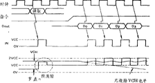
图3是说明按照本发明的一个实施例的升压电路器件基本操作的时序图。图3中,当升压电路器件接到与外部时钟信号CLOCK同步的指令信号COMMAND以读出模式使存储器件操作时,输到或压电路器件的输入信号就与外部时钟信号同步地从0伏变为电源电压VCC。于是,该升压电路器件就在数据输出操作之前执行预激励操作。FIG. 3 is a timing chart illustrating the basic operation of a booster circuit device according to an embodiment of the present invention. In Figure 3, when the boost circuit device receives the instruction signal COMMAND synchronized with the external clock signal CLOCK to operate the storage device in the read mode, the input signal to the OR voltage circuit device is synchronized with the external clock signal from 0 volts becomes the power supply voltage VCC. Then, the booster circuit device performs a pre-drive operation just before a data output operation.
图4表示说明可用于按照本发明一个实施例的升压电路器件的激励电路。Figure 4 shows an illustration of a drive circuit that may be used with a boost circuit device according to one embodiment of the present invention.
本实施例中,送到执行激励操作的MOSFET Q31和Q34栅极的控制脉冲电压由与之相连的电容器C32和C33升压,以便即使电源电压VCC相当低也能获得足够的提升电压。在这种情况下,根据时钟信号CLOCK所产生的输入脉冲信号IN(图3)就通过反相器N31被送入电容器C32的一个电极。电源电压VCC经过以二极管方式连接的MOSFET Q32被送到电容器C32的另一电极。由电容器C32的另一电极所获得的提升的电压被用于控制执行电荷激励操作的MOSFET Q31的栅极电压的开关操作。In this embodiment, the control pulse voltage supplied to the gates of the MOSFETs Q31 and Q34 performing the driving operation is boosted by capacitors C32 and C33 connected thereto so that a sufficient boosted voltage can be obtained even though the power supply voltage VCC is relatively low. In this case, the input pulse signal IN (FIG. 3) generated according to the clock signal CLOCK is sent to one electrode of the capacitor C32 through the inverter N31. The power supply voltage VCC is supplied to the other electrode of the capacitor C32 through the diode-connected MOSFET Q32. The boosted voltage obtained by the other electrode of the capacitor C32 is used to control the switching operation of the gate voltage of the MOSFET Q31 performing the charge excitation operation.
输入脉冲信号IN还通过反相器N32和N34送到电容器C33的一个电极。电容器C33的另一电极与电源电压VCC间设有以二极管方式连接的MOSFET Q33。由电容器C33另一电极取得的提升电压用于控制执行电荷激励操作的MOSFET Q34的栅极电压的开关操作。The input pulse signal IN is also supplied to one electrode of a capacitor C33 through inverters N32 and N34. A MOSFET Q33 is diode-connected between the other electrode of the capacitor C33 and the power supply voltage VCC. The boosted voltage taken from the other electrode of the capacitor C33 is used to control the switching operation of the gate voltage of the MOSFET Q34 which performs the charge excitation operation.
输入脉冲信号IN还通过反相器N32和N33送到电荷抽运电容器C31的一个电极。电容器C31的另一电极经开关MOSFETQ31由电源电压VCC充电。通过MOSFET Q34输出的提升电压使滤波电容器C(图1)充电。The input pulse signal IN is also supplied to one electrode of the charge pumping capacitor C31 through inverters N32 and N33. The other electrode of the capacitor C31 is charged by the power supply voltage VCC via the switching MOSFET Q31. The boost voltage output through MOSFET Q34 charges the filter capacitor C (Figure 1).
图4的激励电路按如下方式工作。当输入脉冲信号IN为低电平时,反相器N31的输出信号则为高电平。此时,反相器N34的输出信号为低电平,使电容器C33经按二极管方式连接的MOSFETQ33预充电。虽然反相器N33的输出信号也为低电平,但MOS-FET Q34和Q31基本被关断。于是,不给电容器C31充电。严格地讲,因节点C由按二极管连接的MOSFET Q33置于VCC-Vth,所以,通过MOSFET Q34向电容器C31的节点a充电到VCC-2Vth。但是,当电源电压VCC为低电压,例如约3.3伏时,给电容器C31充电的电压则是低于1伏的低电压。The drive circuit of Figure 4 works as follows. When the input pulse signal IN is at low level, the output signal of the inverter N31 is at high level. At this time, the output signal of the inverter N34 is at a low level, so that the capacitor C33 is precharged through the diode-connected MOSFET Q33. Although the output signal of the inverter N33 is also at low level, the MOS-FETs Q34 and Q31 are basically turned off. Thus, the capacitor C31 is not charged. Strictly speaking, since the node C is placed at VCC-Vth by the diode-connected MOSFET Q33, the node a of the capacitor C31 is charged to VCC-2Vth through the MOSFET Q34. However, when the power supply voltage VCC is a low voltage, such as about 3.3 volts, the voltage charged to the capacitor C31 is a low voltage of less than 1 volt.
因此,虽然输入信号IN从低电平变到高电平,而由电容器C31获得的提升了的电压VCH却不会达到预定的电压。这意味着,甚至当反相器N34的高电平使电容C33节点C的电压升高而使MOS-FET Q34导通时也不会进行电荷抽运操作。Therefore, although the input signal IN changes from a low level to a high level, the boosted voltage VCH obtained by the capacitor C31 does not reach a predetermined voltage. This means that even when the high level of the inverter N34 raises the voltage of the node C of the capacitor C33 to turn on the MOS-FET Q34, no charge pumping operation is performed.
输入信号IN变成高电平使反相器N31的输出信号变为低电平,从而通过按二极管方式连接的MOSFET Q33向电容器C32充电。因为如上所述,电容器C32已充电,当输入脉冲信号IN再回复到低电平时,电容器C32的升压操作使MOSFET Q31导通,因此将MOSFET Q31充电到电源电压VCC。这就是说,执行预激励操作,以便在输入信号IN的第1脉冲上升边由高电平电压给电容器C32充电,而在输入信号第1脉冲的下降边由低电平电压使电容器C31充电。The input signal IN going high causes the output signal of the inverter N31 to go low, thereby charging the capacitor C32 through the diode-connected MOSFET Q33. As mentioned above, the capacitor C32 has been charged, when the input pulse signal IN returns to low level again, the boost operation of the capacitor C32 turns on the MOSFET Q31, thus charging the MOSFET Q31 to the power supply voltage VCC. That is, a pre-energization operation is performed so that the capacitor C32 is charged with a high-level voltage at the rising edge of the first pulse of the input signal IN, and the capacitor C31 is charged with a low-level voltage at the falling edge of the first pulse of the input signal IN.
图3的时序图中,如上所述,预激励操作是用来对激励电路的电容器C32和C31充电的。由于预激励,当由与输出数据同步进行的预激励操作输出实际上与时钟信号CLOCK同步读出的数据D0-D3时,因数据输出电路操作所造成的提升电压VCH的降低被每次数据输出电路操作时给滤波电容器充电所补偿。结果,提升了的电压VCH能够维持在所要求的高电压电平上。In the timing chart of FIG. 3, the pre-drive operation is used to charge the capacitors C32 and C31 of the drive circuit, as described above. Due to the pre-drive, when the data D0-D3 actually read out synchronously with the clock signal CLOCK are output by the pre-drive operation performed synchronously with the output data, the reduction of the boosted voltage VCH due to the operation of the data output circuit is eliminated every time the data is output. This is compensated by charging the filter capacitor during circuit operation. As a result, the boosted voltage VCH can be maintained at a desired high voltage level.
当如上所述以8比特为一单元来读取数据时,八个数据输出电路DOC1-DOC8同时运行。因此,就要消耗相当大的驱动电流以致降低了提升了的电压VCH。于是,与读出操作同步的激励操作造成数据D0-D3在同样的电压电平下、以同样的输出电流按串行方式从一个输入/输出端I/O输出。When data is read in units of 8 bits as described above, eight data output circuits DOC1-DOC8 operate simultaneously. Therefore, a considerable drive current is consumed to lower the boosted voltage VCH. Thus, the drive operation synchronized with the read operation causes the data D0-D3 to be serially output from one input/output terminal I/O at the same voltage level and at the same output current.
图5是按照本发明一个实施例的升压电路器件的框图。本实施例中,升压电路器件包括多个(例如,4个)激励电路(例如,4a-4d)、一个控制电路40以及一个单(发)脉冲发生器42。这4个激励电路的输出共同连到滤波电容器C。该单发脉冲发生器42响应于指令信号COMMAND产生一个单脉冲,用来设定与外部时钟同步收到的读取模式。控制电路40包括门电路411和后面待详述的分频器/移相器电路412。FIG. 5 is a block diagram of a boost circuit device according to one embodiment of the present invention. In this embodiment, the booster circuit device includes multiple (eg, 4) excitation circuits (eg, 4 a - 4 d ), a
图6是说明图5所示升压电路器件运行的时序图。控制电路40的分频器/移相器电路412将经门电路411接收到的控制脉冲信号IN0的两个频率分频,并把分频后的信号转换成4个彼此相位差为分频后的脉冲信号半周期的相位脉冲信号。换句话说,分频后的输入脉冲信号在相位上依次相差π/2。FIG. 6 is a timing chart illustrating the operation of the booster circuit device shown in FIG. 5 . The frequency divider/
当用由外部时钟信号CLOCK的上升沿引入的指令信号COM-MAND来设置读出模式时,该单发脉冲发生器42随该指令信号(预先输入的信号)而产生单脉冲PREP以执行预激励操作。将脉冲PREP作为基本控制脉冲信号IN0,通过门电路411的NOR门(NOG)送入分频器/移相器电路412。响应从低电平变成高电平的信号IN0,输给第1激励电路4a的输入信号IN1从高电平变成低电平,而输给第2激励电路4b的输入信号IN2从低电平变成高电平。响应从高电平变成低电平的信号IN1,输给第3激励电路4c的输入信号IN3从高电平变成低电平,以及输给第4激励电路4d的输入信号IN4从低电平变成高电平。When the read mode is set with the command signal COM-MAND introduced by the rising edge of the external clock signal CLOCK, the one-
当与外部时钟信号CLOCK同步按串行方式实际输出读出数据D0-D3时,第1激励电路4a输出与输入信号IN0上升边同步的提升电压,而第3激励电路4c输出与输入信号IN0下降沿同步的提升电压。因为激励时间间隔加倍,如上所述,各分频信号依次相移π/2,以执行激励操作,通过第1和第3激励电路4a和4c两次来完成一个数据D0的激励操作。同理,由第2和第4激励电路4b和4d两次来完成数据D1的激励操作。再由第1和第3激励电路4a和4c两次完成数据D2输出的激励操作,而通过第2和第4激励电路4b和4d两次完成数据D3输出的激励操作。When synchronizing with the external clock signal CLOCK and actually outputting the read data D0-D3 in a serial manner, the
如此完善的激励操作进一步抑制了该提升电压VCH的减小,以提供更稳定的提升电压。这就提供更稳定的输出电平和更稳定化的输出电流。Such perfect excitation operation further suppresses the reduction of the boost voltage VCH to provide a more stable boost voltage. This provides a more stable output level and a more stabilized output current.
图7表示一种说明图5实施例控制电路40的具体电路图。把读出指令信号COMMAND供给上面所说的那种单发脉冲发生器42,同时把时钟信号CLOCK和输出启动信号DOE送给门电路411。FIG. 7 shows a specific circuit diagram illustrating the
首先,单发脉冲发生器42响应与外部或输入时钟信号CLOCK同步接收到的读出指令信号COMMAND产生单个信号脉冲PREP。然后,经过门电路411的NOR门NOG和分频器/移相器电路412,将该脉冲PREP送到第1-第4激励电路4a-4d以执行图6所说明的预激励操作。First, the one-
预激励操作之后,NAND门电路NAG被一个其产生时序按一预定模式(称为“等数时间”)控制的数据输出启动信号DOE打开,以便当数据输出有效时,通过NAND门电路NAG引进输入时钟信号,从而使第1至第4激励电路4a-4d依次并与数据输出同步地运行,以便补偿因数据输出而消耗的提升电压的下降。把NAND门NAG的输出经过反相器N41、NOR门NOG和反相器N42作为控制脉冲信号IN0输入到分频器/移相器412中。在图3所示的操作中,该“等数时间”设为3。After the pre-drive operation, the NAND gate circuit NAG is opened by a data output enable signal DOE whose generation timing is controlled by a predetermined pattern (called "equal time"), so that when the data output is valid, the input is introduced through the NAND gate circuit NAG The clock signal, so that the first to
把为DRAM接通电源时所产生的置位脉冲SET加在MOS-FET Q60上,从而令分频器/移相电路412的各节点都处于其起始电压值。电路412包括:接收输入信号IN0和CMOS反相器INV1、接收反相器INV1输出的CMOS反相器INV2,和两个触发器。触发器之一包括同步脉冲反相器(clocked inverter)INV3、接收同步脉冲反相器INV3输出的CMOS反相器INV4,和用来把CMOS反相器INV4的输出信号反馈到它的输入端的同步脉冲反相器INV5,而另一个触发器包括同步脉冲反相器INV6、接收同步脉冲反相器INV6的输出的CMOS反相器INV7,和用来把CMOS反相器INV7的输出信号反馈到它的输入端的同步脉冲反相器INV8。把同步脉冲反相器INV6的输出信号送到CMOS反相器INV7和同步脉冲反相器IN3,以构成二进制计数器(一种分频器)。The set pulse SET generated when the DRAM is powered on is applied to the MOS-FET Q60, so that each node of the frequency divider/
当由于控制脉冲信号IN0处于低电平、分频器/移相器电路412为非操作状态时,同步脉冲反相器INV3和INV8都为关断状态。置位脉冲在预定的时间间隔接通MOSFET Q60,将节点b置为低电平。因为反相器INV5和INV6都为开态,所以,节点a和c都是高电平,而节点b是低电平。When the frequency divider/
通过门电路41接收到的脉冲信号IN0,通过两个反相器INV1和INV2有选择地操作同步脉冲反相器INV3、INV5、INV6和INV8。当输入信号IN0的电平从“低”变“高”时,反相器INV3导通,而反相器INV5和INV6则被关断。因而,节点a从“高”变“低”,而节点b反而从“低”变“高”。此时节点c和d保持不变。当输入信号IN0的电平从“高”变“低”时,反相器INV5和INV6导通,而反相器INV3和INV8被关断。于是,节点c从“高”变“低”,而节点d反而从“低”变“高”。节点a和b保持不变。此后,通过反复类似的操作,在相应节点a-c获得四个不同的依次使相位移动π/2、其周期等于输入信号IN0周期2倍的移相的时钟信号。第1至第4激励电路4a-4d可以具有如图4所示的同样结构。The pulse signal IN0 received through the
图8是按照本发明另一个实施例的升压电路器件的电路图。本实施例设有输出逻辑电平检测电路70,输出一个信号以控制NAND门电路G71-G74,也就是控制由分频器/移相器电路412产生的4个脉冲信号的输出。FIG. 8 is a circuit diagram of a boosting circuit device according to another embodiment of the present invention. In this embodiment, an output logic level detection circuit 70 is provided to output a signal to control the NAND gate circuits G71-G74, that is, to control the output of the four pulse signals generated by the frequency divider/
输出逻辑电平检测电路70检测多个同步输出的数据(例如图1所示结构中的8个数据)的逻辑电平,根据检测结果来控制NAND门电路G71-G74。The output logic level detection circuit 70 detects the logic levels of multiple synchronously output data (for example, 8 data in the structure shown in FIG. 1 ), and controls the NAND gate circuits G71-G74 according to the detection results.
举例来说,当电路70检出所有同时输出的8个数据的第1位数据(DO)全部为低电平时,门电路G71和G73都被电路70的输出关断,以致输给第1充电激励电路4a的输入信号IN1和输给第3充电激励电路4c(图6)的输入信号IN3都保持不变,对第1位的激励决不会起作用。而且,当电路70检出所有同时输出的8个数据的第2位数据(D1)也全都为低电平时,门电路G72和G74被电路70的输出关断,以致输给第2充电激励电路4b的输入信号IN2和输给第4充电激励电路4d(图6)的输入信号IN4保持不变,对第2位的激励也决不会起作用。就这样,可将充电激励电路4a到4d的功率损耗降至最低。For example, when the circuit 70 detects that the first bit data (DO) of all 8 data output at the same time is all low level, the gate circuits G71 and G73 are both turned off by the output of the circuit 70, so that they are output to the first charging Both the input signal IN1 of the
图9是按照本发明又一个实施例的升压电路器件的电路图。本实施例中,图1的两个升压电路器件VCHG1和VCHG2为单一的共用电路所取代。FIG. 9 is a circuit diagram of a boosting circuit device according to yet another embodiment of the present invention. In this embodiment, the two boosting circuit devices VCHG1 and VCHG2 in FIG. 1 are replaced by a single shared circuit.
于是,在门电路411内,以用于提供选通字线用的提升电压VCH的定时接通电源转换开关的时序,将推动激励电路4a-4b的信号供给NOR门电路NOG,该NOR门电路NOG的作用是把输入信号供给反相器N42,以便产生完成上述预激励的输入脉冲信号IN0。Then, in the
VCH电平传感器80能感知该提升电压VCH的电压电平,并能产生第1和第二传感信号CL1和CL2,第1传感信号CL1表示提升电压VCH低于第1电压电平,第2传感信号CL2表示提升电压VCH低于第2电压电平但不低于第1电压电平。举例来说,当电源开关接通时,因为电压VCH为接地电压电平,所以由第1传感信号CL1开启NAND门电路83,以通过NAND门电路83、反相器电路N44和NOR门电路G84引入外部时钟脉冲(CLOCK),直至把电压VCH提升至第1电压电平,例如4V,为止。当电压VCH超过第1电压电平时,由第2传感信号CL2开启NAND门电路G82,以通过NAND门电路G82、反相器电路N43和NOR门电路G84引入来自内部振荡时钟源81的、具有相对长周期的时钟脉冲,直到将电压VCH提升到第2电压电平(例如4.5V)为止。The
另外,通过NOR门电路引入由为选通字线而供给提升电压VCH的定时所产生的单发脉冲REN。In addition, the one-shot pulse REN generated by the timing of supplying the boosted voltage VCH to gate the word line is introduced through the NOR gate circuit.
采取这种结构进行激励,凡是有必要的地方,除数据输出操作的情况外,还通过门电路G84把上述的信号送到门电路411内的NOR门电路NOG,从而使提升的电压保持在基本恒定的电平上。图9所示的实施例,由于共用该升压电路器件,有效地简化了控制电路和激励电路的电路结构。Adopt this structure for excitation, where necessary, except for the case of data output operation, the above-mentioned signal is also sent to the NOR gate circuit NOG in the
图10表示说明按照本发明的一个实施例的DRAM的结构。图10所示的各个电路是采用公知的半导体集成技术形成在单片半导体衬底(例如单晶硅)上的。图10示出半导体芯片上各电路块实际几何布局的实例。在通篇的叙述中,术语“MOSFET”是指一种绝缘栅场效应晶体管(IGFET)。FIG. 10 shows a diagram illustrating the structure of a DRAM according to an embodiment of the present invention. The individual circuits shown in FIG. 10 are formed on a monolithic semiconductor substrate (for example, single crystal silicon) using known semiconductor integration techniques. FIG. 10 shows an example of the actual geometrical layout of circuit blocks on a semiconductor chip. Throughout the description, the term "MOSFET" refers to an insulated gate field effect transistor (IGFET).
为了防止由于增大存储容量而增大芯片尺寸,使得因控制信号和存储阵列驱动信号所用布线导体长度的加长引起RAM操作速度降低,对构成RAM的存储阵列和选择存储阵列地址的外围电路等等的布局作如下设计。In order to prevent the increase of the chip size due to the increase of the storage capacity, the length of the wiring conductor used for the control signal and the storage array driving signal will cause the RAM operation speed to decrease, and the memory array that constitutes the RAM and the peripheral circuit that selects the address of the storage array, etc. The layout is designed as follows.
图10中,在芯片上设置十字形区,它包括垂直的和水平的中心条状部分。各外围电路主要布置在该十字形区上。各存储阵列被布置在四个被十字形区隔开的芯片区。这就是,在芯片的垂直的和水平的中心条状部位设置十字形区,以便将各存储阵列设在四个用十字形区分开的芯片区内。虽然没有具体限制,但四个存储阵列中每个存储容量约为4Mbit,因此总存储容量约为16Mbit。In FIG. 10, a cross-shaped region is provided on the chip, which includes vertical and horizontal central stripes. Peripheral circuits are mainly arranged on the cross-shaped area. Each memory array is arranged in four chip areas separated by cross-shaped areas. That is, cross-shaped areas are provided at the vertical and horizontal center strips of the chip, so that each memory array is provided in four chip areas separated by the cross-shaped areas. Although there is no specific limit, the storage capacity of each of the four storage arrays is about 4Mbit, so the total storage capacity is about 16Mbit.
每个存储阵列包括4个存储块,其中字线沿水平方向延伸,而互补位线(数据线或数字线)对沿垂直方向延伸。一个存储块的存储容量约为1Mbit。每个存储阵列中的四个存储块各有一个字线驱动器(未示出),该驱动器安排在其面对垂直中心条形部位的那一侧的部位。Each memory array includes 4 memory blocks, where word lines extend in the horizontal direction, and complementary bit line (data or digit line) pairs extend in the vertical direction. The storage capacity of one storage block is about 1Mbit. Each of the four memory blocks in each memory array has a word line driver (not shown), which is arranged at its side portion facing the vertical central stripe portion.
行译码器和控制器设在十字形区左边的中心部位,而列译码器和用于字线升压的第1升压电路器件VCHG1则设在十字形区右边的中心部位。The row decoder and the controller are arranged at the center of the left side of the cross-shaped area, while the column decoder and the first booster circuit device VCHG1 for word line boosting are arranged at the center of the right side of the cross-shaped area.
输入/输出缓冲器和输入/输出管脚I/O布置在十字形区的上部中心部位。用于使数据输出缓冲器升压的第2升压电路器件VCHG2设在输入/输出缓冲器下面。The input/output buffer and the input/output pin I/O are arranged in the upper center of the cross-shaped area. A second booster circuit device VCHG2 for boosting the data output buffer is provided below the input/output buffer.
输入缓冲器、相应的地址管脚和时钟管脚都设在十字形区中心部位的下面。虽然未作特别的限制,但是产生其它控制信号RASB、CASB、WEB和CSB的装置都布置在控制器附近的十字形区的中部。The input buffers, corresponding address pins and clock pins are located under the center of the cross-shaped area. Although not particularly limited, means for generating other control signals RASB, CASB, WEB and CSB are arranged in the middle of the cross-shaped area near the controller.
图11是按照本发明一个实施例应用SDRAM的计算机系统的基本部分示意图。该计算机系统包括一总线、一中央处理单元CPU、一外围电路控制器、一作为主存储器的SDRAM及其控制器、一作为备用存储器的SRAM、一备用奇偶检验及其控制单元、一存储程序的ROM,和一显示系统等。FIG. 11 is a schematic diagram of essential parts of a computer system using SDRAM according to an embodiment of the present invention. The computer system includes a bus, a central processing unit CPU, a peripheral circuit controller, a SDRAM as a main memory and its controller, an SRAM as a backup memory, a backup parity check and its control unit, and a stored program ROM, and a display system, etc.
外围电路控制器与外部存储单元、键盘KB等等相连。显示系统包括一VRAM(图象RAM)等,它连接到显示器作为显示存入VRAM内的信息的输出设备。设有把电能供给计算机各内部电路的电源。CPU产生控制各个存储器操作定时的信号。虽然已叙述了把本发明应用于SDRAM作为主存储器的例子,但是如果显示系统的VRAM是多通道式,本发明也可应用于显示系统的VRAM串行存取部件。The peripheral circuit controller is connected with external storage unit, keyboard KB and so on. The display system includes a VRAM (Video RAM), etc., which is connected to the display as an output device for displaying information stored in the VRAM. There is a power supply for supplying electric energy to each internal circuit of the computer. The CPU generates signals that control the timing of individual memory operations. Although an example of applying the present invention to SDRAM as a main memory has been described, the present invention can also be applied to a VRAM serial access unit of a display system if the VRAM of the display system is of a multi-channel type.
当把SDRAM安装在信息处理系统,诸如上述实施例那样的计算机系统上时,由于增加了集成度、扩大了容量、提高了操作速度和/或减小了SDRAM的功耗,可希望得到小型化并增强功能。SDRAM除用作主存储器外,通过有效地利用大容量存储器,SDRAM还可用作文件存储器,来代替硬盘存储器。When SDRAM is mounted on an information processing system, such as a computer system such as the above-described embodiment, miniaturization can be expected due to increased integration, increased capacity, improved operating speed, and/or reduced power consumption of the SDRAM. and enhanced functionality. In addition to being used as a main memory, SDRAM can also be used as a file memory instead of a hard disk memory by effectively utilizing large-capacity memory.
通过上述各实施例所达到的优点如下:The advantages achieved by the above-mentioned embodiments are as follows:
(1)数据输出电路包括两个推挽连接的N-沟输出MOSFET,它连续地输出读出数据。升压电路器件包括两个开关MOSFET,由输入脉冲同步地控制其开关运作,以完成激励操作,以及一激励电路,通过自举电路运作使激励电路升压,而其中控制信号供给这些MOSFET中至少一个的栅极。于是,在读出操作之前进行预激励操作,因而能为激励电路适当地形成提升的电压,结果是,通过由实示读出操作(如见图4)同步的激励操作,能够获得要供给数据输出电路所要求的提升的电压。(1) The data output circuit includes two push-pull connected N-channel output MOSFETs, which continuously output read data. The booster circuit device includes two switching MOSFETs whose switching operation is synchronously controlled by an input pulse to complete an excitation operation, and an excitation circuit for boosting the excitation circuit through a bootstrap circuit operation, wherein a control signal is supplied to at least one of these MOSFETs A grid. Then, the pre-drive operation is performed before the read operation, so that the boosted voltage can be properly formed for the drive circuit, as a result, the data to be supplied can be obtained by the drive operation synchronized by the actual read operation (see FIG. 4, for example). The boosted voltage required by the output circuit.
(2)为了以高速稳定的方式串行输出数据,把升压电路器件应用于存储器,该存储器具有引导指示与外部输入时钟信号同步的操作模式的指令信号以及从存储阵列的位单元读出数据的指示串行输出读出信号的功能。(2) In order to serially output data in a high-speed stable manner, a booster circuit device is applied to a memory having an instruction signal guiding an operation mode synchronous with an external input clock signal and reading data from a bit unit of a memory array The function of indicating the serial output readout signal.
(3)为了稳定所提升的电压,有多个平行输出端的激励电路用于将输入脉冲信号分频为彼此相位不同的多个脉冲信号,因此执行对一个数据输出两次的激励操作(例如,见图7)。(3) In order to stabilize the boosted voltage, an excitation circuit with a plurality of parallel output terminals is used to divide the input pulse signal into a plurality of pulse signals with different phases from each other, thus performing an excitation operation for outputting one data twice (for example, See Figure 7).
(4)连到激励电路输出端的滤波电容器与形成字线选通电压的升压电路器件共用一个输出端,以缩小芯片面积(例如,见图1)。(4) The filter capacitor connected to the output terminal of the driving circuit shares an output terminal with the boost circuit device forming the gate voltage of the word line, so as to reduce the chip area (for example, see FIG. 1 ).
(5)能感受待输出数据逻辑电平,当感知输出为低电平信号时,阻止将输入时钟脉冲传输到激励电路,以减少功耗(例如,见图8)。(5) It can sense the logic level of the data to be output, and when the perceived output is a low-level signal, prevent the input clock pulse from being transmitted to the excitation circuit, so as to reduce power consumption (for example, see FIG. 8 ).
(6)把升压电路器件应用于采用低操作电源电压(例如3伏)的存储器,用以形成充分稳定化的提升的电压,从而提供满意的输出电平和满意的输出电流。(6) Applying a booster circuit device to a memory using a low operating power supply voltage (for example, 3 volts) to form a sufficiently stabilized boosted voltage to provide a satisfactory output level and a satisfactory output current.
(7)当单个升压电路器件具备产生供给字线驱动器的提升的电压和产生供给数据输出电路的提升的电压的双重功能时,就能减小芯片面积(例如,见图9)。(7) When a single boosting circuit device has dual functions of generating a boosted voltage for a word line driver and a boosted voltage for a data output circuit, chip area can be reduced (eg, see FIG. 9 ).
虽然根据最佳实施例,已经具体地描述了本发明,但本发明不限于这些实施例。当然,可以作出许许多多的改变和修改而不偏离本发明的构思。例如,在图2A中,除如上所述的由具有一对NOR门的锁存器形成电平移位部件外,任何只要能把VCC电平转换为VCH电平的电路都可用作电平移位部件。除CMOS反相器外,驱动器电路部件可以有根据输出启动信号关断输出MOSFET Q3的选通功能。Although the present invention has been specifically described based on the preferred embodiments, the present invention is not limited to these embodiments. Of course, numerous changes and modifications can be made without departing from the inventive concept. For example, in Figure 2A, in addition to the above-mentioned level shifting unit formed by a latch with a pair of NOR gates, any circuit that can convert VCC level to VCH level can be used as a level shifter part. In addition to the CMOS inverter, the driver circuit part may have a gating function that turns off the output MOSFET Q3 according to the output enable signal.
DRAM可以有按串行方式用一条字线输出数据的功能。亦即,在该情况下,实现激励操作以防止与时钟信号同步每次输出数据时提升电压的下降。The DRAM may have a function of outputting data in a serial manner with one word line. That is, in this case, an energizing operation is implemented to prevent a drop in boost voltage every time data is output in synchronization with a clock signal.
本发明可广泛地应用于半导体存储装置,它包括按照从升压电路器件产生的驱动信号以传输输出信号的输出电路。The present invention can be widely applied to a semiconductor memory device including an output circuit for transmitting an output signal in accordance with a drive signal generated from a booster circuit device.
Claims (5)
Applications Claiming Priority (2)
| Application Number | Priority Date | Filing Date | Title |
|---|---|---|---|
| JP5121955A JPH06309868A (en) | 1993-04-26 | 1993-04-26 | Semiconductor storage device |
| JP121955/93 | 1993-04-26 |
Publications (2)
| Publication Number | Publication Date |
|---|---|
| CN1095189A CN1095189A (en) | 1994-11-16 |
| CN1034373C true CN1034373C (en) | 1997-03-26 |
Family
ID=14824052
Family Applications (1)
| Application Number | Title | Priority Date | Filing Date |
|---|---|---|---|
| CN94104668A Expired - Fee Related CN1034373C (en) | 1993-04-26 | 1994-04-25 | Boosting circuit device capable of pre-pumping and semiconducotr memory device |
Country Status (4)
| Country | Link |
|---|---|
| US (1) | US5426333A (en) |
| JP (1) | JPH06309868A (en) |
| CN (1) | CN1034373C (en) |
| TW (1) | TW310430B (en) |
Families Citing this family (27)
| Publication number | Priority date | Publication date | Assignee | Title |
|---|---|---|---|---|
| JP3090833B2 (en) * | 1993-12-28 | 2000-09-25 | 株式会社東芝 | Semiconductor storage device |
| JP2679617B2 (en) * | 1994-04-18 | 1997-11-19 | 日本電気株式会社 | Charge pump circuit |
| KR0149224B1 (en) * | 1994-10-13 | 1998-10-01 | 김광호 | Internal Voltage Boost Circuit in Semiconductor Integrated Devices |
| US5677645A (en) * | 1995-05-08 | 1997-10-14 | Micron Technology, Inc. | Vccp pump for low voltage operation |
| JPH0935474A (en) * | 1995-07-19 | 1997-02-07 | Fujitsu Ltd | Semiconductor memory device |
| KR0179852B1 (en) * | 1995-10-25 | 1999-04-15 | 문정환 | Charge pump circuit |
| US5793246A (en) | 1995-11-08 | 1998-08-11 | Altera Corporation | High voltage pump scheme incorporating an overlapping clock |
| KR0170903B1 (en) * | 1995-12-08 | 1999-03-30 | 김주용 | Lower word line driver circuit and semiconductor memory device using same |
| US5767734A (en) * | 1995-12-21 | 1998-06-16 | Altera Corporation | High-voltage pump with initiation scheme |
| KR0172370B1 (en) * | 1995-12-30 | 1999-03-30 | 김광호 | Multistage pumped merged pumping voltage generation circuit |
| JP3768608B2 (en) * | 1996-01-30 | 2006-04-19 | 株式会社日立製作所 | Semiconductor device and semiconductor memory device |
| US5774405A (en) * | 1996-03-28 | 1998-06-30 | Mitsubishi Denki Kabushiki Kaisha | Dynamic random access memory having an internal circuit using a boosted potential |
| US6209071B1 (en) | 1996-05-07 | 2001-03-27 | Rambus Inc. | Asynchronous request/synchronous data dynamic random access memory |
| JPH11260053A (en) | 1998-03-12 | 1999-09-24 | Nec Corp | Step-up circuit of semiconductor memory device |
| JP3346273B2 (en) * | 1998-04-24 | 2002-11-18 | 日本電気株式会社 | Boost circuit and semiconductor memory device |
| US6044026A (en) * | 1998-06-05 | 2000-03-28 | Micron Technology, Inc. | Trap and delay pulse generator for a high speed clock |
| US6628564B1 (en) * | 1998-06-29 | 2003-09-30 | Fujitsu Limited | Semiconductor memory device capable of driving non-selected word lines to first and second potentials |
| KR100557569B1 (en) * | 1998-12-28 | 2006-05-22 | 주식회사 하이닉스반도체 | Charge pump circuit |
| US6320797B1 (en) | 1999-02-24 | 2001-11-20 | Micron Technology, Inc. | Method and circuit for regulating the output voltage from a charge pump circuit, and memory device using same |
| US6160723A (en) | 1999-03-01 | 2000-12-12 | Micron Technology, Inc. | Charge pump circuit including level shifters for threshold voltage cancellation and clock signal boosting, and memory device using same |
| JP2001297584A (en) * | 2000-04-13 | 2001-10-26 | Nec Corp | Boosting circuit of semiconductor memory |
| US6606271B2 (en) * | 2001-05-23 | 2003-08-12 | Mircron Technology, Inc. | Circuit having a controllable slew rate |
| US6717459B2 (en) * | 2002-02-21 | 2004-04-06 | Micron Technology, Inc. | Capacitor charge sharing charge pump |
| KR100604657B1 (en) * | 2004-05-06 | 2006-07-25 | 주식회사 하이닉스반도체 | Semiconductor memory device with power supply circuit that can supply optimized internal voltage |
| JP4785411B2 (en) * | 2004-07-16 | 2011-10-05 | セイコーインスツル株式会社 | Charge pump circuit |
| KR100757410B1 (en) | 2005-09-16 | 2007-09-11 | 삼성전자주식회사 | Phase change memory device and its programming method |
| US10186309B2 (en) * | 2016-06-29 | 2019-01-22 | Samsung Electronics Co., Ltd. | Methods of operating semiconductor memory devices and semiconductor memory devices |
Citations (1)
| Publication number | Priority date | Publication date | Assignee | Title |
|---|---|---|---|---|
| US4794278A (en) * | 1987-12-30 | 1988-12-27 | Intel Corporation | Stable substrate bias generator for MOS circuits |
Family Cites Families (2)
| Publication number | Priority date | Publication date | Assignee | Title |
|---|---|---|---|---|
| US3333205A (en) * | 1964-10-02 | 1967-07-25 | Ibm | Timing signal generator with frequency keyed to input |
| US4670668A (en) * | 1985-05-09 | 1987-06-02 | Advanced Micro Devices, Inc. | Substrate bias generator with power supply control means to sequence application of bias and power to prevent CMOS SCR latch-up |
-
1993
- 1993-04-26 JP JP5121955A patent/JPH06309868A/en active Pending
-
1994
- 1994-04-15 TW TW083103361A patent/TW310430B/zh active
- 1994-04-22 US US08/231,126 patent/US5426333A/en not_active Expired - Fee Related
- 1994-04-25 CN CN94104668A patent/CN1034373C/en not_active Expired - Fee Related
Patent Citations (1)
| Publication number | Priority date | Publication date | Assignee | Title |
|---|---|---|---|---|
| US4794278A (en) * | 1987-12-30 | 1988-12-27 | Intel Corporation | Stable substrate bias generator for MOS circuits |
Also Published As
| Publication number | Publication date |
|---|---|
| TW310430B (en) | 1997-07-11 |
| JPH06309868A (en) | 1994-11-04 |
| US5426333A (en) | 1995-06-20 |
| CN1095189A (en) | 1994-11-16 |
Similar Documents
| Publication | Publication Date | Title |
|---|---|---|
| CN1034373C (en) | Boosting circuit device capable of pre-pumping and semiconducotr memory device | |
| CN1179474C (en) | Booster, integrated circuit card with the booster and electronic equipment | |
| CN1097233C (en) | Word line driving circuit of a semiconductor memory device | |
| CN1113363C (en) | Semiconductor memory device with reduced power consumption and stable operation in data holding state | |
| JP3155879B2 (en) | Semiconductor integrated circuit device | |
| US20050237102A1 (en) | Semiconductor integrated circuit device | |
| CN1210341A (en) | Semiconductor memory device with control for auxiliary word lines for memory cell selection | |
| CN1614716A (en) | Semiconductor memory | |
| CN1627438A (en) | Semiconductor integrated circuit device | |
| CN1448953A (en) | Automatic precharge control circuit in semiconductor memory and method therefor | |
| CN1041580C (en) | Semiconductor memory device | |
| CN1734669A (en) | Semiconductor storage unit and array internal power voltage generating method thereof | |
| CN1117378C (en) | Semiconductor memory having signal input circuit of synchronous type | |
| CN1499527A (en) | Semiconductor memory having self updating for reducing power consumption | |
| CN1169156C (en) | Semiconductor memory with an interface circuit capable of suppressing current consumption | |
| CN1629980A (en) | Semiconductor memory device for reducing address access time | |
| CN1130022C (en) | Semiconductor circuit device operating in synchronization with clock signal | |
| CN1280413A (en) | boost circuit | |
| JP2000100158A (en) | Integrated circuit and synchronous semiconductor memory device | |
| CN1173402C (en) | semiconductor integrated circuit | |
| CN1396600A (en) | Semiconductor memory | |
| JPH05234373A (en) | Semiconductor memory device | |
| US5881000A (en) | Semiconductor memory device having booster supplying step-up voltage exclusively to output circuit for burst | |
| JP2003203491A (en) | Flash memory device | |
| EP0083195A2 (en) | Decoder circuit for a semiconductor device |
Legal Events
| Date | Code | Title | Description |
|---|---|---|---|
| C06 | Publication | ||
| PB01 | Publication | ||
| C10 | Entry into substantive examination | ||
| SE01 | Entry into force of request for substantive examination | ||
| C14 | Grant of patent or utility model | ||
| GR01 | Patent grant | ||
| C19 | Lapse of patent right due to non-payment of the annual fee | ||
| CF01 | Termination of patent right due to non-payment of annual fee |