CN1157759C - Method for mfg. semiconductor device - Google Patents
Method for mfg. semiconductor device Download PDFInfo
- Publication number
- CN1157759C CN1157759C CNB991267273A CN99126727A CN1157759C CN 1157759 C CN1157759 C CN 1157759C CN B991267273 A CNB991267273 A CN B991267273A CN 99126727 A CN99126727 A CN 99126727A CN 1157759 C CN1157759 C CN 1157759C
- Authority
- CN
- China
- Prior art keywords
- laser
- semiconductor film
- crystallization
- tfts
- film
- Prior art date
- Legal status (The legal status is an assumption and is not a legal conclusion. Google has not performed a legal analysis and makes no representation as to the accuracy of the status listed.)
- Expired - Lifetime
Links
- 239000004065 semiconductor Substances 0.000 title claims abstract description 52
- 238000000034 method Methods 0.000 title claims description 55
- 229910021417 amorphous silicon Inorganic materials 0.000 claims abstract description 31
- 238000004519 manufacturing process Methods 0.000 claims abstract description 11
- 229910052710 silicon Inorganic materials 0.000 claims description 43
- 238000002425 crystallisation Methods 0.000 claims description 42
- 239000010703 silicon Substances 0.000 claims description 42
- 230000008025 crystallization Effects 0.000 claims description 41
- PXHVJJICTQNCMI-UHFFFAOYSA-N Nickel Chemical compound [Ni] PXHVJJICTQNCMI-UHFFFAOYSA-N 0.000 claims description 32
- VYPSYNLAJGMNEJ-UHFFFAOYSA-N Silicium dioxide Chemical compound O=[Si]=O VYPSYNLAJGMNEJ-UHFFFAOYSA-N 0.000 claims description 31
- 239000000758 substrate Substances 0.000 claims description 30
- 239000000463 material Substances 0.000 claims description 24
- 238000000137 annealing Methods 0.000 claims description 22
- 230000005855 radiation Effects 0.000 claims description 22
- 238000006555 catalytic reaction Methods 0.000 claims description 17
- 229910052759 nickel Inorganic materials 0.000 claims description 15
- BASFCYQUMIYNBI-UHFFFAOYSA-N platinum Chemical compound [Pt] BASFCYQUMIYNBI-UHFFFAOYSA-N 0.000 claims description 10
- XEEYBQQBJWHFJM-UHFFFAOYSA-N Iron Chemical compound [Fe] XEEYBQQBJWHFJM-UHFFFAOYSA-N 0.000 claims description 9
- 230000001678 irradiating effect Effects 0.000 claims description 6
- 239000000377 silicon dioxide Substances 0.000 claims description 6
- 229910017052 cobalt Inorganic materials 0.000 claims description 5
- 239000010941 cobalt Substances 0.000 claims description 5
- GUTLYIVDDKVIGB-UHFFFAOYSA-N cobalt atom Chemical compound [Co] GUTLYIVDDKVIGB-UHFFFAOYSA-N 0.000 claims description 5
- 229910052697 platinum Inorganic materials 0.000 claims description 5
- 239000011521 glass Substances 0.000 claims description 4
- 238000005468 ion implantation Methods 0.000 claims description 4
- 229910052742 iron Inorganic materials 0.000 claims description 4
- 229910021332 silicide Inorganic materials 0.000 claims description 4
- FVBUAEGBCNSCDD-UHFFFAOYSA-N silicide(4-) Chemical compound [Si-4] FVBUAEGBCNSCDD-UHFFFAOYSA-N 0.000 claims description 4
- -1 phosphonium ion Chemical class 0.000 claims description 3
- 238000005229 chemical vapour deposition Methods 0.000 claims description 2
- 238000010438 heat treatment Methods 0.000 claims 3
- 235000012239 silicon dioxide Nutrition 0.000 claims 1
- 230000003197 catalytic effect Effects 0.000 abstract description 23
- 230000015572 biosynthetic process Effects 0.000 abstract description 10
- 239000010408 film Substances 0.000 description 64
- XUIMIQQOPSSXEZ-UHFFFAOYSA-N Silicon Chemical compound [Si] XUIMIQQOPSSXEZ-UHFFFAOYSA-N 0.000 description 41
- 230000002093 peripheral effect Effects 0.000 description 27
- 229910052814 silicon oxide Inorganic materials 0.000 description 18
- 238000005224 laser annealing Methods 0.000 description 17
- XAGFODPZIPBFFR-UHFFFAOYSA-N aluminium Chemical compound [Al] XAGFODPZIPBFFR-UHFFFAOYSA-N 0.000 description 13
- 229910052782 aluminium Inorganic materials 0.000 description 13
- 239000007789 gas Substances 0.000 description 12
- 239000004411 aluminium Substances 0.000 description 11
- 229910052698 phosphorus Inorganic materials 0.000 description 11
- 239000011574 phosphorus Substances 0.000 description 11
- OAICVXFJPJFONN-UHFFFAOYSA-N Phosphorus Chemical compound [P] OAICVXFJPJFONN-UHFFFAOYSA-N 0.000 description 10
- QVGXLLKOCUKJST-UHFFFAOYSA-N atomic oxygen Chemical compound [O] QVGXLLKOCUKJST-UHFFFAOYSA-N 0.000 description 10
- 239000012535 impurity Substances 0.000 description 10
- 239000001301 oxygen Substances 0.000 description 10
- 229910052760 oxygen Inorganic materials 0.000 description 10
- 238000004544 sputter deposition Methods 0.000 description 9
- XKRFYHLGVUSROY-UHFFFAOYSA-N Argon Chemical compound [Ar] XKRFYHLGVUSROY-UHFFFAOYSA-N 0.000 description 8
- 239000013078 crystal Substances 0.000 description 8
- 238000005516 engineering process Methods 0.000 description 8
- 239000012212 insulator Substances 0.000 description 8
- BOTDANWDWHJENH-UHFFFAOYSA-N Tetraethyl orthosilicate Chemical compound CCO[Si](OCC)(OCC)OCC BOTDANWDWHJENH-UHFFFAOYSA-N 0.000 description 7
- 229910021419 crystalline silicon Inorganic materials 0.000 description 7
- 238000005268 plasma chemical vapour deposition Methods 0.000 description 7
- 230000008569 process Effects 0.000 description 7
- ZOXJGFHDIHLPTG-UHFFFAOYSA-N Boron Chemical compound [B] ZOXJGFHDIHLPTG-UHFFFAOYSA-N 0.000 description 6
- LYCAIKOWRPUZTN-UHFFFAOYSA-N Ethylene glycol Chemical compound OCCO LYCAIKOWRPUZTN-UHFFFAOYSA-N 0.000 description 6
- 229910052796 boron Inorganic materials 0.000 description 6
- 229910052799 carbon Inorganic materials 0.000 description 6
- 239000002019 doping agent Substances 0.000 description 6
- 239000003990 capacitor Substances 0.000 description 5
- 239000001257 hydrogen Substances 0.000 description 5
- 229910052739 hydrogen Inorganic materials 0.000 description 5
- AMGQUBHHOARCQH-UHFFFAOYSA-N indium;oxotin Chemical class [In].[Sn]=O AMGQUBHHOARCQH-UHFFFAOYSA-N 0.000 description 5
- UFHFLCQGNIYNRP-UHFFFAOYSA-N Hydrogen Chemical compound [H][H] UFHFLCQGNIYNRP-UHFFFAOYSA-N 0.000 description 4
- XYFCBTPGUUZFHI-UHFFFAOYSA-N Phosphine Chemical compound P XYFCBTPGUUZFHI-UHFFFAOYSA-N 0.000 description 4
- NRTOMJZYCJJWKI-UHFFFAOYSA-N Titanium nitride Chemical compound [Ti]#N NRTOMJZYCJJWKI-UHFFFAOYSA-N 0.000 description 4
- XSTXAVWGXDQKEL-UHFFFAOYSA-N Trichloroethylene Chemical group ClC=C(Cl)Cl XSTXAVWGXDQKEL-UHFFFAOYSA-N 0.000 description 4
- 239000012190 activator Substances 0.000 description 4
- 229910052786 argon Inorganic materials 0.000 description 4
- 238000000151 deposition Methods 0.000 description 4
- 230000008021 deposition Effects 0.000 description 4
- ZOCHARZZJNPSEU-UHFFFAOYSA-N diboron Chemical compound B#B ZOCHARZZJNPSEU-UHFFFAOYSA-N 0.000 description 4
- 239000007924 injection Substances 0.000 description 4
- 238000002347 injection Methods 0.000 description 4
- 238000005499 laser crystallization Methods 0.000 description 4
- 239000007769 metal material Substances 0.000 description 4
- 239000000203 mixture Substances 0.000 description 4
- UBOXGVDOUJQMTN-UHFFFAOYSA-N trichloroethylene Natural products ClCC(Cl)Cl UBOXGVDOUJQMTN-UHFFFAOYSA-N 0.000 description 4
- 238000004518 low pressure chemical vapour deposition Methods 0.000 description 3
- 229920002120 photoresistant polymer Polymers 0.000 description 3
- 238000012360 testing method Methods 0.000 description 3
- IJGRMHOSHXDMSA-UHFFFAOYSA-N Atomic nitrogen Chemical compound N#N IJGRMHOSHXDMSA-UHFFFAOYSA-N 0.000 description 2
- ZOKXTWBITQBERF-UHFFFAOYSA-N Molybdenum Chemical group [Mo] ZOKXTWBITQBERF-UHFFFAOYSA-N 0.000 description 2
- KDLHZDBZIXYQEI-UHFFFAOYSA-N Palladium Chemical compound [Pd] KDLHZDBZIXYQEI-UHFFFAOYSA-N 0.000 description 2
- RTAQQCXQSZGOHL-UHFFFAOYSA-N Titanium Chemical group [Ti] RTAQQCXQSZGOHL-UHFFFAOYSA-N 0.000 description 2
- 230000008859 change Effects 0.000 description 2
- 238000010586 diagram Methods 0.000 description 2
- 230000008020 evaporation Effects 0.000 description 2
- 238000001704 evaporation Methods 0.000 description 2
- 150000002500 ions Chemical class 0.000 description 2
- 239000004973 liquid crystal related substance Substances 0.000 description 2
- 229910052750 molybdenum Chemical group 0.000 description 2
- 239000011733 molybdenum Chemical group 0.000 description 2
- 229910001453 nickel ion Inorganic materials 0.000 description 2
- 230000003647 oxidation Effects 0.000 description 2
- 238000007254 oxidation reaction Methods 0.000 description 2
- HZBAVWLZSLOCFR-UHFFFAOYSA-N oxosilane Chemical compound [SiH2]=O HZBAVWLZSLOCFR-UHFFFAOYSA-N 0.000 description 2
- 238000005036 potential barrier Methods 0.000 description 2
- 239000002994 raw material Substances 0.000 description 2
- 239000000243 solution Substances 0.000 description 2
- 229910052715 tantalum Inorganic materials 0.000 description 2
- GUVRBAGPIYLISA-UHFFFAOYSA-N tantalum atom Chemical group [Ta] GUVRBAGPIYLISA-UHFFFAOYSA-N 0.000 description 2
- 239000010409 thin film Substances 0.000 description 2
- 239000010936 titanium Chemical group 0.000 description 2
- 229910052719 titanium Inorganic materials 0.000 description 2
- WFKWXMTUELFFGS-UHFFFAOYSA-N tungsten Chemical group [W] WFKWXMTUELFFGS-UHFFFAOYSA-N 0.000 description 2
- 229910052721 tungsten Inorganic materials 0.000 description 2
- 239000010937 tungsten Chemical group 0.000 description 2
- QTBSBXVTEAMEQO-UHFFFAOYSA-M Acetate Chemical compound CC([O-])=O QTBSBXVTEAMEQO-UHFFFAOYSA-M 0.000 description 1
- 229910002651 NO3 Inorganic materials 0.000 description 1
- 229910005883 NiSi Inorganic materials 0.000 description 1
- NHNBFGGVMKEFGY-UHFFFAOYSA-N Nitrate Chemical compound [O-][N+]([O-])=O NHNBFGGVMKEFGY-UHFFFAOYSA-N 0.000 description 1
- 230000001133 acceleration Effects 0.000 description 1
- 239000000654 additive Substances 0.000 description 1
- 230000000996 additive effect Effects 0.000 description 1
- AZDRQVAHHNSJOQ-UHFFFAOYSA-N alumane Chemical group [AlH3] AZDRQVAHHNSJOQ-UHFFFAOYSA-N 0.000 description 1
- 230000008901 benefit Effects 0.000 description 1
- 238000001514 detection method Methods 0.000 description 1
- 238000007598 dipping method Methods 0.000 description 1
- 238000005530 etching Methods 0.000 description 1
- 230000002349 favourable effect Effects 0.000 description 1
- 230000008676 import Effects 0.000 description 1
- 238000001459 lithography Methods 0.000 description 1
- 230000000873 masking effect Effects 0.000 description 1
- 229910052751 metal Inorganic materials 0.000 description 1
- 238000002156 mixing Methods 0.000 description 1
- 150000002815 nickel Chemical class 0.000 description 1
- 229910021334 nickel silicide Inorganic materials 0.000 description 1
- RUFLMLWJRZAWLJ-UHFFFAOYSA-N nickel silicide Chemical compound [Ni]=[Si]=[Ni] RUFLMLWJRZAWLJ-UHFFFAOYSA-N 0.000 description 1
- 229910052757 nitrogen Inorganic materials 0.000 description 1
- 229910052763 palladium Inorganic materials 0.000 description 1
- 239000002245 particle Substances 0.000 description 1
- 238000001259 photo etching Methods 0.000 description 1
- 239000010453 quartz Substances 0.000 description 1
- 150000003839 salts Chemical class 0.000 description 1
- 150000003376 silicon Chemical class 0.000 description 1
- 239000002904 solvent Substances 0.000 description 1
- 238000004528 spin coating Methods 0.000 description 1
- 239000000126 substance Substances 0.000 description 1
- 238000006467 substitution reaction Methods 0.000 description 1
- 238000007738 vacuum evaporation Methods 0.000 description 1
Images


Classifications
-
- H—ELECTRICITY
- H01—ELECTRIC ELEMENTS
- H01L—SEMICONDUCTOR DEVICES NOT COVERED BY CLASS H10
- H01L21/00—Processes or apparatus adapted for the manufacture or treatment of semiconductor or solid state devices or of parts thereof
- H01L21/02—Manufacture or treatment of semiconductor devices or of parts thereof
- H01L21/04—Manufacture or treatment of semiconductor devices or of parts thereof the devices having potential barriers, e.g. a PN junction, depletion layer or carrier concentration layer
- H01L21/18—Manufacture or treatment of semiconductor devices or of parts thereof the devices having potential barriers, e.g. a PN junction, depletion layer or carrier concentration layer the devices having semiconductor bodies comprising elements of Group IV of the Periodic Table or AIIIBV compounds with or without impurities, e.g. doping materials
-
- H—ELECTRICITY
- H01—ELECTRIC ELEMENTS
- H01L—SEMICONDUCTOR DEVICES NOT COVERED BY CLASS H10
- H01L27/00—Devices consisting of a plurality of semiconductor or other solid-state components formed in or on a common substrate
- H01L27/02—Devices consisting of a plurality of semiconductor or other solid-state components formed in or on a common substrate including semiconductor components specially adapted for rectifying, oscillating, amplifying or switching and having potential barriers; including integrated passive circuit elements having potential barriers
- H01L27/12—Devices consisting of a plurality of semiconductor or other solid-state components formed in or on a common substrate including semiconductor components specially adapted for rectifying, oscillating, amplifying or switching and having potential barriers; including integrated passive circuit elements having potential barriers the substrate being other than a semiconductor body, e.g. an insulating body
- H01L27/1214—Devices consisting of a plurality of semiconductor or other solid-state components formed in or on a common substrate including semiconductor components specially adapted for rectifying, oscillating, amplifying or switching and having potential barriers; including integrated passive circuit elements having potential barriers the substrate being other than a semiconductor body, e.g. an insulating body comprising a plurality of TFTs formed on a non-semiconducting substrate, e.g. driving circuits for AMLCDs
- H01L27/1259—Multistep manufacturing methods
- H01L27/127—Multistep manufacturing methods with a particular formation, treatment or patterning of the active layer specially adapted to the circuit arrangement
- H01L27/1274—Multistep manufacturing methods with a particular formation, treatment or patterning of the active layer specially adapted to the circuit arrangement using crystallisation of amorphous semiconductor or recrystallisation of crystalline semiconductor
- H01L27/1277—Multistep manufacturing methods with a particular formation, treatment or patterning of the active layer specially adapted to the circuit arrangement using crystallisation of amorphous semiconductor or recrystallisation of crystalline semiconductor using a crystallisation promoting species, e.g. local introduction of Ni catalyst
-
- G—PHYSICS
- G02—OPTICS
- G02F—OPTICAL DEVICES OR ARRANGEMENTS FOR THE CONTROL OF LIGHT BY MODIFICATION OF THE OPTICAL PROPERTIES OF THE MEDIA OF THE ELEMENTS INVOLVED THEREIN; NON-LINEAR OPTICS; FREQUENCY-CHANGING OF LIGHT; OPTICAL LOGIC ELEMENTS; OPTICAL ANALOGUE/DIGITAL CONVERTERS
- G02F1/00—Devices or arrangements for the control of the intensity, colour, phase, polarisation or direction of light arriving from an independent light source, e.g. switching, gating or modulating; Non-linear optics
- G02F1/01—Devices or arrangements for the control of the intensity, colour, phase, polarisation or direction of light arriving from an independent light source, e.g. switching, gating or modulating; Non-linear optics for the control of the intensity, phase, polarisation or colour
- G02F1/13—Devices or arrangements for the control of the intensity, colour, phase, polarisation or direction of light arriving from an independent light source, e.g. switching, gating or modulating; Non-linear optics for the control of the intensity, phase, polarisation or colour based on liquid crystals, e.g. single liquid crystal display cells
- G02F1/133—Constructional arrangements; Operation of liquid crystal cells; Circuit arrangements
- G02F1/1333—Constructional arrangements; Manufacturing methods
- G02F1/1345—Conductors connecting electrodes to cell terminals
- G02F1/13454—Drivers integrated on the active matrix substrate
-
- H—ELECTRICITY
- H01—ELECTRIC ELEMENTS
- H01L—SEMICONDUCTOR DEVICES NOT COVERED BY CLASS H10
- H01L21/00—Processes or apparatus adapted for the manufacture or treatment of semiconductor or solid state devices or of parts thereof
- H01L21/02—Manufacture or treatment of semiconductor devices or of parts thereof
- H01L21/02104—Forming layers
- H01L21/02365—Forming inorganic semiconducting materials on a substrate
- H01L21/02518—Deposited layers
- H01L21/02521—Materials
- H01L21/02524—Group 14 semiconducting materials
- H01L21/02532—Silicon, silicon germanium, germanium
-
- H—ELECTRICITY
- H01—ELECTRIC ELEMENTS
- H01L—SEMICONDUCTOR DEVICES NOT COVERED BY CLASS H10
- H01L21/00—Processes or apparatus adapted for the manufacture or treatment of semiconductor or solid state devices or of parts thereof
- H01L21/02—Manufacture or treatment of semiconductor devices or of parts thereof
- H01L21/02104—Forming layers
- H01L21/02365—Forming inorganic semiconducting materials on a substrate
- H01L21/02656—Special treatments
- H01L21/02664—Aftertreatments
- H01L21/02667—Crystallisation or recrystallisation of non-monocrystalline semiconductor materials, e.g. regrowth
- H01L21/02672—Crystallisation or recrystallisation of non-monocrystalline semiconductor materials, e.g. regrowth using crystallisation enhancing elements
-
- H—ELECTRICITY
- H01—ELECTRIC ELEMENTS
- H01L—SEMICONDUCTOR DEVICES NOT COVERED BY CLASS H10
- H01L21/00—Processes or apparatus adapted for the manufacture or treatment of semiconductor or solid state devices or of parts thereof
- H01L21/02—Manufacture or treatment of semiconductor devices or of parts thereof
- H01L21/02104—Forming layers
- H01L21/02365—Forming inorganic semiconducting materials on a substrate
- H01L21/02656—Special treatments
- H01L21/02664—Aftertreatments
- H01L21/02667—Crystallisation or recrystallisation of non-monocrystalline semiconductor materials, e.g. regrowth
- H01L21/02675—Crystallisation or recrystallisation of non-monocrystalline semiconductor materials, e.g. regrowth using laser beams
- H01L21/02686—Pulsed laser beam
Landscapes
- Engineering & Computer Science (AREA)
- Power Engineering (AREA)
- Chemical & Material Sciences (AREA)
- Crystallography & Structural Chemistry (AREA)
- Condensed Matter Physics & Semiconductors (AREA)
- Physics & Mathematics (AREA)
- Manufacturing & Machinery (AREA)
- General Physics & Mathematics (AREA)
- Computer Hardware Design (AREA)
- Microelectronics & Electronic Packaging (AREA)
- Chemical Kinetics & Catalysis (AREA)
- Recrystallisation Techniques (AREA)
- Thin Film Transistor (AREA)
Abstract
Method of fabricating a semiconductor circuit is initiated with formation of an amorphous silicon film. Then, a second layer containing at least one catalytic element is so formed as to be in intimate contact with the amorphous silicon film, or the catalytic element is introduced into the amorphous silicon film. This amorphous silicon film is selectively irradiated with laser light or other equivalent intense light to crystallize the amorphous silicon film.
Description
Technical field
The method that the present invention relates to thin-film transistor (TFTs) and make TFTs.The method that the present invention relates to use the semiconductor circuit of a plurality of TFTs in addition and make this semiconductor device.Or, form thin-film transistor made in accordance with the present invention in dielectric substrate such as glass or on the silicon single crystal Semiconductor substrate.Especially the present invention is applicable to semiconductor device, and this device comprises the low speed array circuit and is used to drive the high-speed peripheral circuit of array circuit, for example is used for driving the monolithic active array circuit of liquid crystal display pipe.The present invention has very big advantage.
Background technology
In recent years, studied the insulated gate semiconductor device of film-type active layer (also claiming active region).Especially conscientiously studied the film-type gated transistor that is called TFT.On transparent dielectric substrate, form this transistorlike, perhaps in order to each pixel in the display device that is controlled at all liquid crystal displays if any array structure or in order to constitute drive circuit.According to employed semiconducting crystal state or material, they are classified as non-crystalline silicon tft s or crystalline silicon TFTs.
Usually, amorphous semiconductor has little field mobility, and therefore, they can not be used for the TFTs that requires high speed operation.So, in recent years, studied crystalline silicon TFTs, and carried out and made device with higher characteristic.
Because crystalline semiconductor has higher field mobility than amorphous semiconductor, so crystalline semiconductor can be with higher speed operation.With regard to crystalline silicon, can make PMOSTFTs and NMOS TFTs.For example, the well-known peripheral circuit of forming active display LCD by the CMOS crystal TFTs that is similar to the active array circuit part.In other words, this is a kind of single chip architecture.
Fig. 3 is the block diagram as the monolithic active array circuit of LCD.On substrate 7, constitute column decoder 1 and row decoder 2, to form peripheral drive circuit.Form each at array region 3 and comprise the pixel circuit 4 of a transistor and a capacitor.By conductive interconnection line 5 and 6 array region is connected with peripheral circuit.The TFTs that is used for peripheral circuit is required that with high speed operation the TFTs that is used for pixel circuit simultaneously also is required to have low-leakage current.Physically, these are conflicting characteristics, but must form this two class TFTs on same substrate simultaneously.
Yet, demonstrate identical characteristic with all TFTs of identical technical process manufacturing.As using TFTs all to have identical characteristic by the crystalline silicon TFTs of thermal annealing manufacturing, the TFTs that is used for array region and peripheral drive circuit.Be difficult to obtain simultaneously to be suitable for the low-leakage current and the high mobility that is applicable to peripheral drive circuit of pixel circuit.By using thermal annealing simultaneously and utilizing selective laser annealing crystallizationization just can solve above-mentioned difficulties.In this case, can use the TFTs that makes by thermal annealing at array region, and can use the TFTs that makes by laser annealing in peripheral drive circuit area.But, utilize the uniformity of degree of crystallinity of silicon of laser annealing crystallization very low, especially, in requiring flawless peripheral drive circuit, be difficult to use these TFTs.
In order to obtain crystalline silicon, also can use the crystallization process that depends on laser annealing.If this silicon by the laser annealing crystallization is made semiconductor device, all has identical characteristic at the TFTs of array region with TFTs so at peripheral drive circuit.Therefore, can imagine the method that another kind makes crystallization of silicon.Especially utilize thermal annealing to be formed on the TFTs of array region, utilize laser annealing to be formed on the TFTs of peripheral drive circuit.Yet, adopt thermal annealing, must under 600 ℃ of temperature, reach and 24 hours make annealed silicon, or must make annealed silicon above under 1000 ℃ the high temperature.Former approach productivity ratio is low; Latter's method can with backing material be confined to quartz.
Summary of the invention
The object of the invention is to provide a kind of method of making semiconductor device, and this method does not rely on complicated technical process, does not influence output or production cost.
Another object of the present invention is to provide a kind of method, and this method has minimum technique change, is easy to produce in a large number two kinds of TFTs.Wherein a kind of requirement has high mobility, and another kind of requirement has low-leakage current.
Our research discloses: increase micro-catalysis material and promote crystallization for amorphous silicon film in fact, reduce crystallization temperature, shorten crystallization time.The example of catalysis material comprises the single component material of nickel (Ni), iron (Fe), cobalt (Co), platinum and silicide thereof.Or rather, use the film that contains this catalytic elements, elementary particle or element set, at first film of formation up and down of amorphous silicon, so that first film is closely contacted with amorphous silicon film.On the other hand, with ion injection or additive method such catalytic elements is injected into amorphous silicon film.Then, under proper temperature film is made thermal annealing, general temperature is lower than 580 ℃, and the time foreshortened in 8 hours.Amorphous film is by crystallization as a result.
Make with such catalytic elements under the situation of film, the concentration of element is fully low, so film is very thin.Can use the method for vacuum pump such as sputter or vacuum evaporation to form this film.In addition, also can adopt under normal pressure as the method that spin applies or dipping is realized.This is easy to implement with the normal pressure method, and high productivity ratio is provided.In this case, comprising acetate, nitrate, such catalytic elements such as organic salt is dissolved in the appropriate solvent, and its concentration is adjusted to suitable value.
When forming amorphous silicon film, catalysis material is added in the raw gas, when forming amorphous silicon film, can be added to catalysis material in the evaporation source of target or formation film with physical evaporation deposit such as sputter by the CVD method.Certainly, rise with annealing temperature, crystallization time reduces.In addition, increase with nickel, iron, cobalt and platinum concentration, crystallization temperature descends, and crystallization time shortens.Studies show that: in order to promote crystallization, the concentration of one of these elements must surpass 10 at least
17/ cm
3, surpass 5 * 10
18/ cm
3Better.
Because whole above-mentioned catalysis materials are not that silicon is desired, so wish that their concentration is low as far as possible.Our research discloses: the total concentration of these catalysis materials preferably is no more than 1 * 10
20/ cm
3, and preferably the local concentration concentration of crystal boundary place (for example) is no more than 1 * 20
20/ cm
3
In the present invention, optionally form high speed operation and be used as the TFTs that drives active array circuit TFTs by laser crystallization.On the other hand, by the actual use of the crystallographic property that promotes by above-mentioned catalytic elements, make with than low velocity work and as the TFTs of the low-leakage current TFTs of active array circuit pixel.For forming latter TFTs, make crystallization of silicon in the short time at low temperatures.As a result, on same substrate, can form comprise a plurality of transistorized, should realize that low-leakage current is realized high speed operation again, these two characteristic is conflicting circuit usually.
Also find: when the rayed that equals laser with laser or intensity contains the film of catalytic elements such as nickel, iron, cobalt, platinum and palladium, even the concentration ratio of catalytic elements causes that the concentration of crystallization is much smaller in that thermal equilibrium state is usually required, very fast crystal growth also takes place.Be typically, the former concentration is less than 1/10th of latter's concentration.
More particularly, adjust to 1 * 10 by concentration these catalytic elements
15~1 * 10
19/ cm
3, be 1 * 10 preferably
16~5 * 10
17/ cm
3Also can promote crystallization.Then, with the laser of suitable energy or this film of rayed of other suitable intensity, the energy density of the light that laser or other intensity equate changes, and depends on temperature (or crystalline silicon) and other factors of irradiation light wavelength, pulse duration, amorphous silicon film.For example, if the temperature of amorphous silicon is transferred to 100-450 ℃, be 250~350 ℃ preferably, also can finish crystallization with less catalytic elements concentration.
The present invention utilizes the characteristic of above-mentioned catalysis material crystallization to form amorphous silicon film.The film of being made by the material that contains catalytic elements closely is connected with amorphous silicon film, or element adds to amorphous silicon film, equals the rayed amorphous film of laser then with laser or intensity, so that the amorphous silicon film crystallization.At this moment, the material that contains catalytic elements closely contacts or mixes these parts with the selection part of substrate.Then, equal the rayed of laser or scan this film with laser or intensity.Use this method, on same substrate, can form the different silicon fiml of degree of crystallinity.Before laser radiation, also can be preferably under 400~550 ℃ at 350~650 ℃, through 1~24 hour, be preferably 2~8 hours and make preannealing.
Can improve degree of crystallinity with this method.In addition, though make the inexpungible crystal boundary potential barrier of thermal annealing, as long as it is all right to reduce the crystal boundary potential barrier.In addition, even can make the amorphous position crystallization of staying crystal boundary.This method that is adopted in this case even the degree of crystallinity that reaches by thermal annealing descends, also can be finished whole crystallizations by follow-up laser radiation.Therefore can reduce the concentration of utilizing catalytic elements.
In the present invention, improve with catalytic elements doped regions degree of crystallinity by follow-up laser radiation, be better than the less regional degree of crystallinity of doping with catalytic elements, and no matter before laser radiation, whether implemented annealing.In addition, the characteristic of the TFTs that obtains performance be equivalent to or be better than by TFTs characteristic with the general laser annealing manufacturing of laser radiation amorphous film.Herein, the energy that used laser or intensity equal the light of laser is less than the laser energy of using in common laser annealing, just can stably obtain these characteristics.On the other hand, also can make catalytic elements doped regions of no use crystallization through laser radiation.And in this case, make the energy of light that laser or intensity equals laser, also can obtain stable properties less than the laser energy that in common laser annealing, uses.Certainly, catalytic elements doped regions characteristic of no use will be inferior to those characteristics with the catalytic elements doped regions.
Utilize these characteristics, the catalytic elements lightly doped region is used to form the low-leakage current TFTs in the pixel circuit of active array circuit.And the catalytic elements heavily doped region is used for the high-speed type TFTs of peripheral drive circuit.As a result, can form so a kind of circuit on a substrate, this circuit comprises that obtaining existing low-leakage current has high speed operation again, often conflicting each transistor of characteristic.
In the present invention, the catalytic elements concentration in formation requires the TFTs part of low-leakage current must be lower than the concentration of the catalytic elements in the part of formation high speed TFTs.For the difference that makes them becomes bigger or reduces leakage current again, the concentration of the metallic element in the source region of TFTs that needs low-leakage current is preferably less than 1 * 10
15/ cm
3
By description below, other purposes of the present invention and characteristics can be clearer.
Description of drawings
Fig. 1 (A)~1 (E) is the semiconductor device profile according to the embodiment of the invention 1, and each step of carrying out continuously of making semiconductor device is described;
Fig. 2 (A)~2 (E) is the profile that is similar to Fig. 1 (A)~1 (E), and the semiconductor device according to embodiment 2 is described;
Fig. 3 is the schematic diagram of monolithic active array circuit;
Fig. 4 (A)~4 (E) is the profile according to the embodiment of the invention 3; Each step of carrying out continuously of making semiconductor device is described; And,
Fig. 5 (A)~5 (E) is the profile that is similar to Fig. 4 (A)~4 (E), and the semiconductor device according to embodiment 4 is described.
Embodiment
Embodiment 1
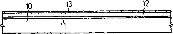
Present embodiment relates to a kind of semiconductor device, and as shown in Figure 3, this semiconductor device is included in active array circuit that forms on the single glass substrate and the drive circuit that forms around the active array circuit.Fig. 1 (A)~(E) is the drawing in side sectional elevation according to the present embodiment semiconductor device, and each step of making this device continuously is described.At first, on the substrate of making by Corn-ing7059 10 thick 2000 of sputter silica as counterdie 11.Form on silicon oxide layer 11 with the LPCVD method and to have 500~1500 , the intrinsic amorphous silicon film 12 that for example 1500 are thick.After this immediately by sputtering deposit nickle silicide thickness be 5~200 for example 20 as film 13 (Figure 1A).The chemical molecular formula of nickel silicide film 13 is NiSi
x, and 0.4≤X≤2.5, for example X=20.
Then, shine this laminated product selectively, so that should select regional crystallization with laser.Use as irradiates light and to have 248nm wavelength and pulse duration light as the KrF excimer laser emission of 20nsec.Other lasers can be used the light as the XeF excimer laser emission of wavelength 353nm, and wavelength is the light of the XeCl quasi-molecule laser emission of 308nm, and wavelength is the light of the ArF excimer laser emission of 193nm, and other lasers.Laser energy density is 200~500mJ/cm
2, 350mJ/cm for example
2Launch laser 2~10 times in each position, for example 2 times.During laser radiation, substrate is heated to 200~450 ℃, as 300 ℃.
As shown in Figure 3, the peripheral circuit region that utilize the laser radiation crystallization be enough to bear by the array circuit of the thermal anneal process very big distance of being separated by.Therefore need not lithography step.
In reducing atmosphere environment, under 500 ℃ conditions make laminated product do 4 hour annealing, so that the zone of of no use laser radiation (pixel circuit of active array circuit) crystallization thereafter.As a result, obtain two kinds of silicon metal zone 12a and 12b.By the laser crystallization step, improved the field mobility of regional 12a, otherwise, then become low-leakage current district (Fig. 1 (B)) by the regional 12b of thermal annealing crystallization.
To carry out photoetching composition with the silicon fiml that the method obtains, with island silicon area 14a that is shaped as peripheral drive circuit and the island areas 14b that forms array circuitry area.By sputter, deposition thickness is that the silica of 1000 is as gate insulating film 15.When sputtering technology, use the target of silicon oxide-containing.During sputter, underlayer temperature is 200~400 ℃ for example 350 ℃.The sputter ambiance contains oxygen and argon.The ratio of argon and oxygen is between 0 and 0.5, for example less than 0.1.Utilize the LPVD deposition thickness to reach for example 6000 of 6000~8000 , contain the silicon of 0.1~2% phosphorus, to form silicon fiml.Preferably form the step of silicon oxide layer and the step of formation silicon fiml continuously.Silicon fiml is carried out composition to form gate electrode 16a, 16b and 16c (Fig. 1 (C)).
Then, shelter silicon area, utilize the plasma doping method that the impurity that comprises phosphorus or boron is injected silicon area with gate electrode.Hydrogen phosphide (PH
3) and diborane (B
2H
6) as gas dopant.During a kind of gas, accelerating voltage is 60~90KV, as 80KV before using; When using a kind of gas in back, accelerating voltage is 40~80KV such as 65KV.Dosage is 1 * 10
16~8 * 10
16/ cm
2Dosage is 2 * 10 under with the phosphorus situation
15/ cm
2Dosage is 5 * 10 under with the boron situation
15/ cm
2As a result, form N type doped region 17a, P type doped region 17b and 17c.
Thereafter, by the laser annealing activator impurity.Use wavelength to do laser annealing as the light of the KrF excimer laser emission of 20nsec as 248nm and pulse duration, other lasers are the light of the XeF excimer laser emission of 353nm such as wavelength, wavelength is the light of the XeCL excimer laser emission of 308nm, and other laser all can use.Laser energy density is 200~400mJ/cm
2, such as 250mJ/cm
2, during the laser radiation, such as 2 times, substrate can be heated to 200~400 ℃ to each position emission laser 2~10 times.Can under 450~500 ℃ of temperature, do annealing in 2~8 hours rather than laser radiation to laminated product.Use this method, make doped region 17a~17c activate (Fig. 1 (D)).
Then, by plasma CVD, the thick silica of deposit 6000 is as interlevel insulator 18.Then sputter thickness is the indium tin oxides (ITO) of 500~1000 such as 800 , and composition is to form pixel capacitors 19.In interlevel insulator 18, form contact hole.Be configured for forming the electrode of TFTs of peripheral drive circuit and each conductive interconnection line 20a, 20b, 20c by the multilayer film of metal material such as titanium nitride and aluminium, and electrode and each conductive interconnection line 20d of being used to form the TFTs of array pixel circuit, 20e.At last, in the hydrogen environment, an atmospheric pressure, temperature is to make this laminated product through annealing in 30 minutes under 350 ℃ the condition.Like this, just finished semiconductor device (Fig. 1 (E)).
Measure the interior nickel concentration of active region of the TFTs that is obtained with ion microprobe (SIMS).For peripheral drive circuit and array circuit, concentration is 1 * 10
18~5 * 10
18/ cm
3
Embodiment 2
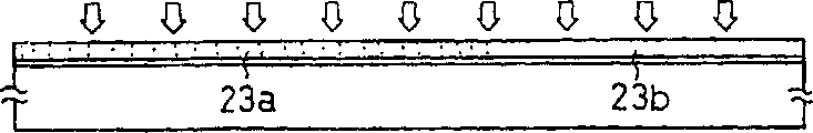
Fig. 2 (A)~2 (E) is a drawing in side sectional elevation, and this figure illustrates each the continuous execution in step that constitutes this embodiment.On the substrate 21 that is made of Corning7509, the sputter silica is thick to be 2000 , as silicon oxide layer 22.And utilizing LPCVD to form thickness on silicon oxide layer 22 is for example amorphous silicon films 23 of 500 of 200~1500 .Inject nickel ion, form zone 24, and the nickel concentration of mixing that should zone 24 is 1 * 10 on the amorphous silicon film surface
18~2 * 10
19/ cm
3For example 5 * 10
18/ cm
3The degree of depth of doped region 24 is 200~500 .Also select acceleration energy (Fig. 2 (A)) according to the degree of depth of doped region.
And, with laser to the irradiation of electing property of amorphous silicon film, so that selected position crystallization.As laser radiation is that wavelength is the light of 248nm with the KrF excimer laser emission of pulse duration 20nsec.The energy density of laser is 200-500mJ/cm
2, 350mJ/cm for example
2Launch laser 2~10 times in each position, for example 2 times.During laser radiation, substrate is heated to 200~450 ℃ for example 400 ℃.In reducing atmosphere, temperature is under 500 ℃, makes laminated product through 4 hours annealing, so that the not position crystallization of illuminated mistake of amorphous silicon film.As the result of this crystallisation step, obtain the silicon area 23a and the 23b (Fig. 2 (B)) of two kinds of crystallizations.
, make silicon fiml composition, to form island areas 26a (peripheral drive circuit zone) and 26b (array resembles the rope circuit region) thereafter.As the gate insulating film of TFTs, by tetrem oxosilane [tetraethyl orthosilicate, Si (OC
2H
5)
4] and oxygen to form thickness be the silicon oxide layer 27 of 1000 .Also with trichloroethylene (C
2HCl
3) be added in the unstrpped gas.Before this film is shaped, be flow that the oxygen of 400SCCM is sent into chamber.At underlayer temperature is 300 ℃, total pressure 5Pa, and RF power is that 150W produces plasma down.This condition kept 10 minutes.Then respectively with 300SCCM, the flow of 15SCCM and 2SCCM is oxygen, and tetraethyl orthosilicate and trichloroethylene import chamber.So just form silicon oxide layer, and substrate temperature is 300 ℃, RF power is 75W, and stagnation pressure is for being 5Pa.After film is made, under the pressure of 100torr, hydrogen is imported chamber.Under 350 ℃ of temperature, with this laminated product annealing 35 minutes.
Then, with sputtering method deposition thickness 6000~8000 as the aluminium that contains 2% silicon of 6000 as the aluminium film.Also available tantalum, tungsten, titanium or molybdenum substitution of Al.Preferably carry out step that forms silicon oxide layer 27 and the step that forms the aluminium film continuously.The aluminium film is carved into figure, to form gate electrode 28a, 28b and the 28c of TFTs.Anodic oxidation is done on the surface of aluminum interconnecting, formed oxide layer 29a, 29b and 29c on the surface.In tartaric 1~5% ethylene glycol solution, implement anodized.The thickness of oxide layer that obtains is 2000 (Fig. 2 (C)).
Utilize the plasma doping method then, impurity or phosphorus are injected into silicon area.Utilize hydrogen phosphide (PH
3) as gas dopant, accelerating voltage is for example 80KV of 60~90KV.Dosage is 1 * 10
15~8 * 10
15/ cm
2So just form N type doped region 30a.Shelter the TFT (N channel TFT) on the left side with photoresist, with the plasma doping method impurity or boron are injected into the silicon area of the peripheral circuit region TFT on the right and the silicon area that injects forming array circuit TFTs again.Utilize diborane (B
2H
6) be for example 65KV of 50~80KV as the gas dopant accelerating voltage, dosage is 1 * 10
15~8 * 10
15/ cm
2For example 5 * 10
15/ cm
2For example 5 * 10
15/ cm
2, above-mentioned dosage is greater than the dosage of previous injection phosphorus.P type doped region and 30c have so just been formed.
Then, use the laser annealing activator impurity.The wavelength that has as laser radiation is the light of the KrF excimer laser emission of 248nm and pulse duration 20nsec.Laser energy density is 200~400mJ/cm
2250mJ/cm for example
2To 2~10 times for example twice of each position irradiating laser (Fig. 2 (D)).
Then, by plasma CVD, form the silicon oxide layer 31 of 2000 ° of A of thickness as interlevel insulator with tetraethyl orthosilicate (TEOS).Utilize sputtering method, deposit 500~1000 indium tin oxide (ITO) that for example 800 are thick is as indium tin oxygen oxide-film.This film of etching forms pixel capacitors 32.In interlevel insulator 31, form contact hole.By metal material for example the multilayer film of titanium nitride and aluminium form source, drain electrode, be used for conductive interconnection line 33a, 33b, 33c and each electrode of TFTs of peripheral drive circuit and conductive interconnection line 33d, the 33e that is used for the TFTs of array pixel circuit.So just finished semiconductor device (Fig. 2 (E)).
The performance of making the peripheral drive circuit TFTs of semiconductor device never is inferior to the TFTs performance of making of the prior art laser crystallization.Utilization constitutes shift register according to these TFTs of present embodiment.We are levies in kind: use the 15V drain voltage, this shift register can be worked under 11MHz, uses the 17V drain voltage, then can work under 16MHz.And in reliability testing, do not find out between novel TFTs and the TFTs there are differences by the manufacturing of known technology method.With regard to regard to the performance of the TFTs in the array region pixel circuit, leakage current is less than 10
-13A.
Embodiment 3
Fig. 4 (A)~4 (E) is the transverse cross-sectional view of semiconductor device, and all figure illustrate manufacturing each continuous execution in step according to the present embodiment device.At first, the silica of 2000 ° of A of sputter thickness on the substrate of being made by Corning7059 is as bottom 11.Utilizing plasma CVD to form thickness in basic unit 11 is for example intrinsic of 500 (I) type amorphous silicon films 12 of 500~1500 .Then, use sputtering method immediately, it is 1 * 10 that formation selectively contains concentration
18/ cm
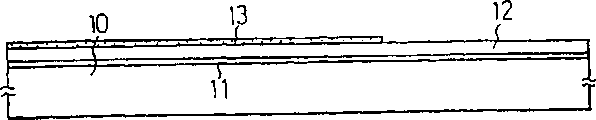
3Nickel and with thickness be 5~200 for example 50 silicon fiml 13 as shown.Utilization is peeled off (lift-off) technology and is made this nickel film 13.Also can use spin-coating method to replace sputtering method (Fig. 4 (A)).
Whole surface with laser radiation amorphous silicon film 12 makes its crystallization.With regard to this laser radiation, can use wavelength to be 248nm and pulse duration light as the KrF excimer laser emission of 20nsec.
Also available other lasers such as wavelength are the XeF excimer laser of 353nm, and wavelength is the XeCl quasi-molecule laser of 308nm, and to be that the ArF of 193nm is accurate send out sub-laser and other lasers to wavelength.The energy density of laser is 200~500mJ/cm
2, 350mJ/cm for example
2Launch laser 2~10 times to each position, for example 2 times.During laser radiation, substrate is heated to 100~450 ℃, for example 300 ℃.As a result, make the whole surface crystallizationization of amorphous silicon film.Yet the degree of crystallinity that is positioned at those positions of silicon fiml 12a below the tantnickel film 13 is better than the degree of crystallinity at other zones silicon fiml 2b, and this is to have promoted crystallization (Fig. 4 (B)) because of nickel.
Silicon fiml is photo-etched into figure, to form island silicon area 14a (peripheral drive circuit zone) and 14b (array region).Use sputtering method, the thick Si oxide of deposit 1000 is as gate insulating film 15.In sputtering technology, use the target of silicon oxide-containing.In this technical process, substrate temperature is 200~400 ℃, for example 350 ℃.The atmosphere of sputter contains oxygen and argon.The ratio of argon and oxygen is between 0 and 0.5, for example less than 0.1.Then, by the LPCVD method, forming thick is 3000~8000 , for example 6000 and the silicon fiml that contains 0.1~2% phosphorus.Best, as to implement to form the step of silicon oxide layer 15 continuously and form silicon fiml step.Again silicon fiml is carved into figure, to form gate electrode 16a, 16b and 16C (Fig. 4 (C)).
So, utilize gate electrode as mask, use the plasma doping method, impurity or phosphorus and boron injection silicon area.Hydrogen phosphide (PH
3) and diborane (B
2H
6) all can be used as dopant gas.When using hydrogen phosphide, accelerating voltage is 60~90KV, for example 80KV; When using diborane, accelerating voltage is 40~80KV, for example 65KV.Dosage is 1 * 10
15~8 * 10
15/ cm
2For example phosphorus dosage is 2 * 10
15/ cm
2The dosage of boron is 5 * 10
15/ cm
2, the result has formed N type doped region 17a, P type doped region 17b, 17c.
After this, by the laser annealing activator impurity.With regard to this laser annealing, use the light of wavelength as the KrF excimer laser emission of 248nm and pulse duration 20nsec.The wavelength of other lasers such as the emission of XeF excimer laser is that the light of 353nm, the wavelength of XeCl quasi-molecule laser emission are that the wavelength that the light of 308nm, ArF excimer laser are launched is the light of 193nm and the light of other laser.The energy density of laser is 200~400mJ/cm
2250mJ/cm for example
2To each position irradiating laser 2~10 times, for example 2 times.During laser annealing, substrate is heated to 100~450 ℃, for example 250 ℃.So just activated doped region 17a~17c (Fig. 4 D).
Then, use plasma CVD method, forming thickness is the interior insulator of silicon oxide layer 18 conduct layers of 6000 .Forming thickness by sputter is for example indium tin oxide films of 800 (ITO) of 500~1000 .This film is carved into figure, forms pixel capacitors 19.In interlevel insulator, form contact hole again.With the metal material multilayer film formation electrode of titanium nitride and aluminium for example, conductive interconnection line 20a, 20b, 20c and the electrode of the TFTs of peripheral drive circuit, and conductive interconnection line 20d, 20e and the electrode of the TFTs of array pixel circuit.At last under 350 ℃, 1 atmospheric pressure and in the hydrogen environment through 30 minutes, make laminated product annealing.Like this, just finished semiconductor device (Fig. 4 (E)).
With SIMS test decide present embodiment obtain in the TFTs active region nickeliferous concentration, the nickel concentration in the peripheral drive circuit among the TFTs is 1 * 10
17~5 * 10
17/ cm
3Nickel concentration in the pixel circuit among the TFTs is lower than the detection lower limit, is limited to 1 * 10 under this
16/ cm
3
Embodiment 4
Fig. 5 (A)~5 (E) is the drawing in side sectional elevation of semiconductor device.All figure illustrate each step of making continuously according to the device of present embodiment.Utilization sputters on the substrate of being made by Corn-ing7059 21, forms the silicon oxide layer 22 of thickness 2000 .Then, use plasma CVD method, forming thickness on silicon oxide layer 22 is for example amorphous silicon films 23 of 500 of 200~1500 .24 sheltering this film simultaneously with photoresist, use ion implantation, selectively nickel ion is injected in the amorphous silicon film 23.Like this, forming concentration is 1 * 10
15~1 * 10
18/ cm
3For example 5 * 10
16/ cm
3Nickeliferous regional 25.The degree of depth in these zones 25 is 200~500 .Determine accelerating voltage according to this degree of depth.Because present embodiment adopts ion implantation, aspect the control nickel concentration compared with the technology of embodiment 3 just more effectively (Fig. 5 (A)).Then, at 350~650 ℃, preferably 400~550 ℃ for example 500 ℃, in blanket of nitrogen, made substrate annealing 2 hours.As a result of, the crystallization process of nickel doped region tentatively obtains advancing, and then, the whole surface with laser radiation amorphous silicon film 23 makes these regional crystallization.With regard to this laser radiation, use the light of the KrF excimer laser emission of wavelength 248nm and pulse duration 20nsec.The energy density of laser is 200~500mJ/cm
2350mJ/cm for example
2To each position emission laser 2~10, for example 2 times.During laser radiation, substrate is heated to 100~450 ℃ for example 350 ℃.As a result, silicon fiml crystallization.Those regional 23a with nickel doping silicon fiml are being better than not doped region 23b (Fig. 5 (B)) aspect the degree of crystallinity.
, make silicon fiml be carved into figure, form island silicon area 26a (peripheral drive circuit zone) and 26b (array pixel circuit zone) thereafter.Use plasma CVD method, form the gate insulating film of the silicon oxide layer 27 of thickness 1000 as TFTs, said process uses tetrem oxosilane (tetraethyl orthosilicate Si (OC
2H
5)
4) and oxygen as gas raw material.Trichloroethylene (C
2HCl
3) be added in the gas raw material.Before film is shaped, oxygen is sent in the chamber with the flow of 400SCCM.At underlayer temperature is 300 ℃, and total pressure is 5Pa, and RF power is to produce plasma under the 150W condition.Then, with the flow of 300SCCM, 15SCCM and 2SCCM oxygen, tetraethyl orthosilicate and trichloroethylene are imported chamber respectively.So just form silicon oxide layer.Substrate temperature is 300 ℃, and RF power is 75W, and total pressure is 5Pa.After doing film forming, hydrogen is imported in 100torr pressure lower chambers.Under 350 ℃, laminated product is annealed again through 35 minutes.
Then, be 6000~8000 with the sputtering method deposition thickness, the aluminium that contains 2% silicon of 6000 for example.Also available tantalum, tungsten, titanium or molybdenum replace aluminium.Preferably implement to form the step of silicon oxide layer 27 and the step of formation aluminium film continuously.The aluminium film is carved into figure, forms TFTs gate electrode 28a, 28b and 28c.Make aluminum interconnecting surface anodic oxidation, to form oxide layer 29a, 29b and 29c on the surface.In tartaric 1~5% ethylene glycol solution, carry out anodized.The oxidated layer thickness that obtains is 2000 (Fig. 5 C).
Use the plasma doping method, impurity, or phosphorus injects silicon area.With phosphorus hydrogen (PH
3) as gas dopant.Accelerating voltage is 60~90KV, for example 80KV.Dosage is 1 * 10
15~8 * 10
15/ cm
2For example 2 * 10
15/ cm
2So just form N type doped region 30a.TFT (N channel TFT) by the photoresist masking left side utilizes the plasma doping method once more, and impurity, or boron injects the silicon area and the silicon area that forms array circuit TFTs of the peripheral circuit region TFT on the right.Diborane (B
2H
6) as gas dopant.Accelerating voltage is 50~80KV, for example 6 5KV.Dosage is 1 * 10
15~8 * 10
15/ cm
2, for example 5 * 10
15/ cm
2, this dosage is greater than the dosage at this injection phosphorus.Just use this method, form P type doped region 30b and 30c.
After this, by the laser annealing activator impurity.With regard to this laser annealing, can use the light of the KrF excimer laser emission of wavelength 248nm and pulse duration 20nsec.The energy density of laser is 200~400mJ/cm
2, 250mJ/cm for example
2Launch laser 2~10 times to each position, for example 2 times (Fig. 2 (D)).
Then, by plasma CVD method, forming thickness by tetraethyl orthosilicate is that the silicon oxide layer 31 of 2000 is as interlevel insulator.By sputter, forming thickness is 500~1000 , for example the indium tin oxide film of 800 (ITO).This film is carved into figure, forms pixel capacitors 32.Then, in interlevel insulator 31, form contact hole.By metal material, as the TFTs electrode of the multilayer film formation peripheral drive circuit of titanium nitride and aluminium and electrical interconnection line 33a, 33b, 33c, and the electrode of the TFTs of array pixel circuit and conductive interconnection line 33d, 33e.Like this, just finished semiconductor device (Fig. 5 (E)).
The performance of the TFTs of the peripheral drive circuit of made semiconductor device never is lower than the performance of the TFTs that is made by known laser crystallization technology.Utilization constitutes shift register according to these TFTs of present embodiment.We confirm: use the 15V drain voltage, shift register can be worked under 11MHz, uses the 17V drain voltage, and then shift register can be worked under 16MHz.Also have, in reliability testing, do not observe novel TFTs and the TFTs that makes by the known technology method between difference.With regard to the performance of the interior TFTs of array region (pixel circuit), leakage current is less than 10
-13A.
As described in above-mentioned embodiment, the present invention can make the TFTs of energy high speed operation and demonstrate the TFTs of low-leakage current on same substrate.This structure can be applicable to LCD, be easy to produce in enormous quantities TFTs, and performance improves.Certainly, on substrate, also can make the TFTs that only shows one of these two features.
In addition, in the present invention can also low temperature, as 500 ℃ and in short-term, make crystallization of silicon as 4 hours, and improve productivity ratio.Employing is higher than 600 ℃ of traditional handicrafts of carrying out, and can make the glass substrate change of contracting, distortion, and the rate that causes manufacturing a finished product descends.And adopt the present invention that this problem is resolved fully.This also means: have very large-area substrate with handling in the once-through operation.Especially, by large-area substrate is cut into many semiconductor device,, can greatly reduce the price of each device like this such as array circuit.So, the present invention is to industrial more favourable.
Claims (19)
1. method of making semiconductor device comprises:
On an insulating surface, form the semiconductor film that contains amorphous silicon;
Form the catalysis material that contacts with described semiconductor film at least a portion, this catalysis material is used to promote the crystallization of described semiconductor film; Then,
With described semiconductor film and the described catalysis material that contains amorphous silicon of laser radiation, so that this semiconductor film crystallization.
2. the method for claim 1 is characterized in that, described catalysis material is selected from nickel, iron, cobalt, platinum and one group of material of its silicide.
3. the method for claim 1 is characterized in that, described catalysis material forms with ion implantation.
4. the method for claim 1 is characterized in that, carries out described irradiating laser and heating simultaneously so that described semiconductor film crystallization.
5. the method for claim 1 is characterized in that, and is further comprising the steps of:
After described irradiating step, phosphonium ion is introduced in the part of described semiconductor film; Then,
Make described semiconductor film annealing more than two hours or two hours in temperature more than 450 ° or 450 ℃.
6. the method for claim 1 is characterized in that, described insulating surface is the surface of glass substrate.
7. the method for claim 1 is characterized in that, described insulating surface is the surface of silicon dioxide film.
8. method according to claim 1 is characterized in that described semiconductor film forms with the CVD method.
9. the method for claim 1 is characterized in that, described laser is pulse type laser.
10. the method for claim 1 is characterized in that, described laser is excimer laser.
11. method as claimed in claim 10 is characterized in that, described excimer laser is selected from a kind of in one group of KrF excimer laser, XeF excimer laser, XeCl excimer laser and the ArF excimer laser.
12. the method for claim 1 is characterized in that, the energy density of described laser is 200 to 500mJ/cm
2
13. the method for claim 1 is characterized in that, described insulating surface is a surface of silicon.
14. a method of making semiconductor device comprises:
On an insulating surface, form the semiconductor film that contains amorphous silicon;
Form the catalysis material that contacts with described semiconductor film at least a portion, this catalysis material is used to promote the crystallization of described semiconductor film;
To described semiconductor film and the heating of described catalysis material, so that this semiconductor film crystallization; Know
Semiconductor film with laser radiation crystallization.
15. method as claimed in claim 14 is characterized in that, to described semiconductor film annealing, annealing temperature is 400 to 550 ℃.
16. method as claimed in claim 14 is characterized in that, described catalysis material is selected from nickel, iron, cobalt, platinum and one group of material of its silicide.
17. method as claimed in claim 14 is characterized in that, described catalysis material forms with ion implantation.
18. method as claimed in claim 14 is characterized in that, carries out described irradiating laser and heating simultaneously so that described semiconductor film crystallization.
19. method as claimed in claim 14 is characterized in that, and is further comprising the steps of:
After described irradiating step, phosphonium ion is introduced in the part of described semiconductor film; Then,
Make described semiconductor film annealing more than two hours or two hours in temperature more than 450 ° or 450 ℃.
Applications Claiming Priority (4)
| Application Number | Priority Date | Filing Date | Title |
|---|---|---|---|
| JP79005/1993 | 1993-03-12 | ||
| JP79004/1993 | 1993-03-12 | ||
| JP7900493A JP3359690B2 (en) | 1993-03-12 | 1993-03-12 | Method for manufacturing semiconductor circuit |
| JP7900593 | 1993-03-12 |
Related Parent Applications (1)
| Application Number | Title | Priority Date | Filing Date |
|---|---|---|---|
| CN94104267A Division CN1092844C (en) | 1993-03-12 | 1994-03-12 | Semiconductors circuit and method of fabrication the same |
Publications (2)
| Publication Number | Publication Date |
|---|---|
| CN1255733A CN1255733A (en) | 2000-06-07 |
| CN1157759C true CN1157759C (en) | 2004-07-14 |
Family
ID=26420092
Family Applications (4)
| Application Number | Title | Priority Date | Filing Date |
|---|---|---|---|
| CNB991267273A Expired - Lifetime CN1157759C (en) | 1993-03-12 | 1994-03-12 | Method for mfg. semiconductor device |
| CN94104267A Expired - Fee Related CN1092844C (en) | 1993-03-12 | 1994-03-12 | Semiconductors circuit and method of fabrication the same |
| CNB011166339A Expired - Fee Related CN1305107C (en) | 1993-03-12 | 1994-03-12 | Semiconductor circuit and its manufacturing method |
| CNB991103912A Expired - Lifetime CN1136612C (en) | 1993-03-12 | 1999-07-16 | Semiconductor circuits and manufacture thereof |
Family Applications After (3)
| Application Number | Title | Priority Date | Filing Date |
|---|---|---|---|
| CN94104267A Expired - Fee Related CN1092844C (en) | 1993-03-12 | 1994-03-12 | Semiconductors circuit and method of fabrication the same |
| CNB011166339A Expired - Fee Related CN1305107C (en) | 1993-03-12 | 1994-03-12 | Semiconductor circuit and its manufacturing method |
| CNB991103912A Expired - Lifetime CN1136612C (en) | 1993-03-12 | 1999-07-16 | Semiconductor circuits and manufacture thereof |
Country Status (4)
| Country | Link |
|---|---|
| US (4) | US5569610A (en) |
| KR (1) | KR0171437B1 (en) |
| CN (4) | CN1157759C (en) |
| TW (1) | TW241377B (en) |
Families Citing this family (202)
| Publication number | Priority date | Publication date | Assignee | Title |
|---|---|---|---|---|
| US6975296B1 (en) * | 1991-06-14 | 2005-12-13 | Semiconductor Energy Laboratory Co., Ltd. | Electro-optical device and method of driving the same |
| CN1244891C (en) * | 1992-08-27 | 2006-03-08 | 株式会社半导体能源研究所 | Active matrix display |
| US5403762A (en) | 1993-06-30 | 1995-04-04 | Semiconductor Energy Laboratory Co., Ltd. | Method of fabricating a TFT |
| US6323071B1 (en) | 1992-12-04 | 2001-11-27 | Semiconductor Energy Laboratory Co., Ltd. | Method for forming a semiconductor device |
| TW226478B (en) * | 1992-12-04 | 1994-07-11 | Semiconductor Energy Res Co Ltd | Semiconductor device and method for manufacturing the same |
| US6997985B1 (en) | 1993-02-15 | 2006-02-14 | Semiconductor Energy Laboratory Co., Ltd. | Semiconductor, semiconductor device, and method for fabricating the same |
| JP3562588B2 (en) | 1993-02-15 | 2004-09-08 | 株式会社半導体エネルギー研究所 | Method for manufacturing semiconductor device |
| EP0612102B1 (en) * | 1993-02-15 | 2001-09-26 | Semiconductor Energy Laboratory Co., Ltd. | Process for the fabrication of a crystallised semiconductor layer |
| TW241377B (en) | 1993-03-12 | 1995-02-21 | Semiconductor Energy Res Co Ltd | |
| US6413805B1 (en) * | 1993-03-12 | 2002-07-02 | Semiconductor Energy Laboratory Co., Ltd. | Semiconductor device forming method |
| JP3535205B2 (en) * | 1993-03-22 | 2004-06-07 | 株式会社半導体エネルギー研究所 | Method for manufacturing thin film transistor |
| US6090646A (en) | 1993-05-26 | 2000-07-18 | Semiconductor Energy Laboratory Co., Ltd. | Method for producing semiconductor device |
| US5818076A (en) | 1993-05-26 | 1998-10-06 | Semiconductor Energy Laboratory Co., Ltd. | Transistor and semiconductor device |
| KR100355938B1 (en) * | 1993-05-26 | 2002-12-16 | 가부시키가이샤 한도오따이 에네루기 켄큐쇼 | Semiconductor device manufacturing method |
| KR100186886B1 (en) * | 1993-05-26 | 1999-04-15 | 야마자끼 승페이 | Semiconductor device manufacturing method |
| JPH06349735A (en) * | 1993-06-12 | 1994-12-22 | Semiconductor Energy Lab Co Ltd | Semiconductor device |
| US5488000A (en) | 1993-06-22 | 1996-01-30 | Semiconductor Energy Laboratory Co., Ltd. | Method of fabricating a thin film transistor using a nickel silicide layer to promote crystallization of the amorphous silicon layer |
| US6713330B1 (en) | 1993-06-22 | 2004-03-30 | Semiconductor Energy Laboratory Co., Ltd. | Method of fabricating a thin film transistor |
| US5663077A (en) * | 1993-07-27 | 1997-09-02 | Semiconductor Energy Laboratory Co., Ltd. | Method of manufacturing a thin film transistor in which the gate insulator comprises two oxide films |
| JP2814049B2 (en) * | 1993-08-27 | 1998-10-22 | 株式会社半導体エネルギー研究所 | Semiconductor device and manufacturing method thereof |
| US6777763B1 (en) * | 1993-10-01 | 2004-08-17 | Semiconductor Energy Laboratory Co., Ltd. | Semiconductor device and method for fabricating the same |
| JP3030368B2 (en) | 1993-10-01 | 2000-04-10 | 株式会社半導体エネルギー研究所 | Semiconductor device and manufacturing method thereof |
| US5869362A (en) * | 1993-12-02 | 1999-02-09 | Semiconductor Energy Laboratory Co., Ltd. | Method of manufacturing semiconductor device |
| CN1156918C (en) | 1993-12-02 | 2004-07-07 | 株式会社半导体能源研究所 | Semicondutor device |
| US6798023B1 (en) | 1993-12-02 | 2004-09-28 | Semiconductor Energy Laboratory Co., Ltd. | Semiconductor device comprising first insulating film, second insulating film comprising organic resin on the first insulating film, and pixel electrode over the second insulating film |
| TW272319B (en) * | 1993-12-20 | 1996-03-11 | Sharp Kk | |
| KR100319332B1 (en) | 1993-12-22 | 2002-04-22 | 야마자끼 순페이 | Semiconductor device and electro-optical device |
| JP3221473B2 (en) | 1994-02-03 | 2001-10-22 | 株式会社半導体エネルギー研究所 | Method for manufacturing semiconductor device |
| JP3195157B2 (en) * | 1994-03-28 | 2001-08-06 | シャープ株式会社 | Semiconductor device manufacturing method and its manufacturing apparatus |
| US6059873A (en) | 1994-05-30 | 2000-05-09 | Semiconductor Energy Laboratory Co., Ltd. | Optical processing method with control of the illumination energy of laser light |
| US5650636A (en) | 1994-06-02 | 1997-07-22 | Semiconductor Energy Laboratory Co., Ltd. | Active matrix display and electrooptical device |
| JP3067949B2 (en) * | 1994-06-15 | 2000-07-24 | シャープ株式会社 | Electronic device and liquid crystal display device |
| TW273639B (en) * | 1994-07-01 | 1996-04-01 | Handotai Energy Kenkyusho Kk | Method for producing semiconductor device |
| TW280943B (en) * | 1994-07-15 | 1996-07-11 | Sharp Kk | |
| TW345705B (en) | 1994-07-28 | 1998-11-21 | Handotai Energy Kenkyusho Kk | Laser processing method |
| JP3072005B2 (en) * | 1994-08-25 | 2000-07-31 | シャープ株式会社 | Semiconductor device and manufacturing method thereof |
| JPH0869967A (en) | 1994-08-26 | 1996-03-12 | Semiconductor Energy Lab Co Ltd | Manufacturing method of semiconductor device |
| TW395008B (en) * | 1994-08-29 | 2000-06-21 | Semiconductor Energy Lab | Semiconductor circuit for electro-optical device and method of manufacturing the same |
| JP3442500B2 (en) | 1994-08-31 | 2003-09-02 | 株式会社半導体エネルギー研究所 | Method for manufacturing semiconductor circuit |
| TW374247B (en) * | 1994-09-15 | 1999-11-11 | Semiconductor Energy Lab Co Ltd | Method of fabricating semiconductor device |
| US5712191A (en) * | 1994-09-16 | 1998-01-27 | Semiconductor Energy Laboratory Co., Ltd. | Method for producing semiconductor device |
| US6242289B1 (en) | 1995-09-08 | 2001-06-05 | Semiconductor Energy Laboratories Co., Ltd. | Method for producing semiconductor device |
| US5818068A (en) * | 1994-09-22 | 1998-10-06 | Sharp Kabushiki Kaisha | Thin film transistor circuit and an active matrix type display device |
| USRE43450E1 (en) | 1994-09-29 | 2012-06-05 | Semiconductor Energy Laboratory Co., Ltd. | Method for fabricating semiconductor thin film |
| US6300659B1 (en) | 1994-09-30 | 2001-10-09 | Semiconductor Energy Laboratory Co., Ltd. | Thin-film transistor and fabrication method for same |
| US5915174A (en) * | 1994-09-30 | 1999-06-22 | Semiconductor Energy Laboratory Co., Ltd. | Semiconductor device and method for producing the same |
| US5942768A (en) * | 1994-10-07 | 1999-08-24 | Semionductor Energy Laboratory Co., Ltd. | Semiconductor device having improved crystal orientation |
| US5756364A (en) * | 1994-11-29 | 1998-05-26 | Semiconductor Energy Laboratory Co., Ltd. | Laser processing method of semiconductor device using a catalyst |
| US6008101A (en) * | 1994-11-29 | 1999-12-28 | Semiconductor Energy Laboratory Co., Ltd. | Laser processing method of semiconductor device |
| US6337229B1 (en) | 1994-12-16 | 2002-01-08 | Semiconductor Energy Laboratory Co., Ltd. | Method of making crystal silicon semiconductor and thin film transistor |
| JP2900229B2 (en) | 1994-12-27 | 1999-06-02 | 株式会社半導体エネルギー研究所 | Semiconductor device, manufacturing method thereof, and electro-optical device |
| US6331475B1 (en) | 1995-01-12 | 2001-12-18 | Semiconductor Energy Laboratory Co., Ltd. | Method and manufacturing semiconductor device |
| US5929464A (en) * | 1995-01-20 | 1999-07-27 | Semiconductor Energy Laboratory Co., Ltd. | Active matrix electro-optical device |
| JP4130237B2 (en) * | 1995-01-28 | 2008-08-06 | 株式会社半導体エネルギー研究所 | Method for manufacturing crystalline silicon film and method for manufacturing semiconductor device |
| TW305063B (en) | 1995-02-02 | 1997-05-11 | Handotai Energy Kenkyusho Kk | |
| JP3364081B2 (en) | 1995-02-16 | 2003-01-08 | 株式会社半導体エネルギー研究所 | Method for manufacturing semiconductor device |
| JP3778456B2 (en) | 1995-02-21 | 2006-05-24 | 株式会社半導体エネルギー研究所 | Method for manufacturing insulated gate thin film semiconductor device |
| US5757456A (en) * | 1995-03-10 | 1998-05-26 | Semiconductor Energy Laboratory Co., Ltd. | Display device and method of fabricating involving peeling circuits from one substrate and mounting on other |
| JP3138169B2 (en) * | 1995-03-13 | 2001-02-26 | シャープ株式会社 | Method for manufacturing semiconductor device |
| US5834327A (en) | 1995-03-18 | 1998-11-10 | Semiconductor Energy Laboratory Co., Ltd. | Method for producing display device |
| US7075002B1 (en) | 1995-03-27 | 2006-07-11 | Semiconductor Energy Laboratory Company, Ltd. | Thin-film photoelectric conversion device and a method of manufacturing the same |
| KR100265179B1 (en) | 1995-03-27 | 2000-09-15 | 야마자끼 순페이 | Semiconductor device and manufacturing method thereof |
| TW463378B (en) | 1995-06-01 | 2001-11-11 | Semiconductor Energy Lab | Method of manufacturing semiconductor device |
| US6337109B1 (en) * | 1995-06-07 | 2002-01-08 | Semiconductor Energy Laboratory Co., Ltd. | Method of producing crystalline semiconductor |
| JP4056571B2 (en) | 1995-08-02 | 2008-03-05 | 株式会社半導体エネルギー研究所 | Method for manufacturing semiconductor device |
| JP3295679B2 (en) * | 1995-08-04 | 2002-06-24 | 株式会社半導体エネルギー研究所 | Method for manufacturing semiconductor device |
| JPH0951035A (en) * | 1995-08-07 | 1997-02-18 | Mitsubishi Electric Corp | Formation of interlayer insulation layer |
| JP3917205B2 (en) * | 1995-11-30 | 2007-05-23 | 株式会社半導体エネルギー研究所 | Method for manufacturing semiconductor device |
| JP3907726B2 (en) | 1995-12-09 | 2007-04-18 | 株式会社半導体エネルギー研究所 | Method for manufacturing microcrystalline silicon film, method for manufacturing semiconductor device, and method for manufacturing photoelectric conversion device |
| JP3124480B2 (en) * | 1995-12-12 | 2001-01-15 | 株式会社半導体エネルギー研究所 | Method for manufacturing semiconductor device |
| US6204101B1 (en) | 1995-12-15 | 2001-03-20 | Semiconductor Energy Laboratory Co., Ltd. | Method of manufacturing semiconductor device |
| TW319912B (en) * | 1995-12-15 | 1997-11-11 | Handotai Energy Kenkyusho Kk | |
| JP3645379B2 (en) * | 1996-01-19 | 2005-05-11 | 株式会社半導体エネルギー研究所 | Method for manufacturing semiconductor device |
| JP3729955B2 (en) * | 1996-01-19 | 2005-12-21 | 株式会社半導体エネルギー研究所 | Method for manufacturing semiconductor device |
| US5985740A (en) * | 1996-01-19 | 1999-11-16 | Semiconductor Energy Laboratory Co., Ltd. | Method of manufacturing a semiconductor device including reduction of a catalyst |
| JP3645380B2 (en) | 1996-01-19 | 2005-05-11 | 株式会社半導体エネルギー研究所 | Manufacturing method of semiconductor device, information terminal, head mounted display, navigation system, mobile phone, video camera, projection display device |
| US6478263B1 (en) | 1997-01-17 | 2002-11-12 | Semiconductor Energy Laboratory Co., Ltd. | Semiconductor device and its manufacturing method |
| JP3645378B2 (en) * | 1996-01-19 | 2005-05-11 | 株式会社半導体エネルギー研究所 | Method for manufacturing semiconductor device |
| US5888858A (en) | 1996-01-20 | 1999-03-30 | Semiconductor Energy Laboratory Co., Ltd. | Semiconductor device and fabrication method thereof |
| US6180439B1 (en) | 1996-01-26 | 2001-01-30 | Semiconductor Energy Laboratory Co., Ltd. | Method for fabricating a semiconductor device |
| US7056381B1 (en) | 1996-01-26 | 2006-06-06 | Semiconductor Energy Laboratory Co., Ltd. | Fabrication method of semiconductor device |
| US6465287B1 (en) * | 1996-01-27 | 2002-10-15 | Semiconductor Energy Laboratory Co., Ltd. | Method for fabricating a semiconductor device using a metal catalyst and high temperature crystallization |
| US6063654A (en) * | 1996-02-20 | 2000-05-16 | Semiconductor Energy Laboratory Co., Ltd. | Method of manufacturing a thin film transistor involving laser treatment |
| TW317643B (en) * | 1996-02-23 | 1997-10-11 | Handotai Energy Kenkyusho Kk | |
| TW335503B (en) | 1996-02-23 | 1998-07-01 | Semiconductor Energy Lab Kk | Semiconductor thin film and manufacturing method and semiconductor device and its manufacturing method |
| TW374196B (en) | 1996-02-23 | 1999-11-11 | Semiconductor Energy Lab Co Ltd | Semiconductor thin film and method for manufacturing the same and semiconductor device and method for manufacturing the same |
| JP3472024B2 (en) | 1996-02-26 | 2003-12-02 | 株式会社半導体エネルギー研究所 | Method for manufacturing semiconductor device |
| US6100562A (en) * | 1996-03-17 | 2000-08-08 | Semiconductor Energy Laboratory Co., Ltd. | Method of manufacturing a semiconductor device |
| US6133119A (en) * | 1996-07-08 | 2000-10-17 | Semiconductor Energy Laboratory Co., Ltd. | Photoelectric conversion device and method manufacturing same |
| US5773329A (en) * | 1996-07-24 | 1998-06-30 | International Business Machines Corporation | Polysilicon grown by pulsed rapid thermal annealing |
| JPH10199807A (en) | 1996-12-27 | 1998-07-31 | Semiconductor Energy Lab Co Ltd | Manufacture of crystalline silicon film |
| TW386238B (en) | 1997-01-20 | 2000-04-01 | Semiconductor Energy Lab | Semiconductor device and method of manufacturing the same |
| JPH10214974A (en) * | 1997-01-28 | 1998-08-11 | Semiconductor Energy Lab Co Ltd | Semiconductor device and its fabrication |
| US6830616B1 (en) * | 1997-02-10 | 2004-12-14 | Semiconductor Energy Laboratory Co., Ltd. | Manufacturing method of semiconductor and manufacturing method of semiconductor device |
| JP4242461B2 (en) | 1997-02-24 | 2009-03-25 | 株式会社半導体エネルギー研究所 | Method for manufacturing semiconductor device |
| JP3544280B2 (en) | 1997-03-27 | 2004-07-21 | 株式会社半導体エネルギー研究所 | Method for manufacturing semiconductor device |
| JPH10282414A (en) * | 1997-04-09 | 1998-10-23 | Canon Inc | Zoom lens |
| JP3376247B2 (en) * | 1997-05-30 | 2003-02-10 | 株式会社半導体エネルギー研究所 | Thin film transistor and semiconductor device using thin film transistor |
| US6541793B2 (en) | 1997-05-30 | 2003-04-01 | Semiconductor Energy Laboratory Co., Ltd. | Thin-film transistor and semiconductor device using thin-film transistors |
| US6307214B1 (en) | 1997-06-06 | 2001-10-23 | Semiconductor Energy Laboratory Co., Ltd. | Semiconductor thin film and semiconductor device |
| JP3844561B2 (en) * | 1997-06-10 | 2006-11-15 | 株式会社半導体エネルギー研究所 | Method for manufacturing semiconductor device |
| US6501094B1 (en) | 1997-06-11 | 2002-12-31 | Semiconductor Energy Laboratory Co., Ltd. | Semiconductor device comprising a bottom gate type thin film transistor |
| JP3717634B2 (en) * | 1997-06-17 | 2005-11-16 | 株式会社半導体エネルギー研究所 | Method for manufacturing semiconductor device |
| JP3295346B2 (en) | 1997-07-14 | 2002-06-24 | 株式会社半導体エネルギー研究所 | Method for producing crystalline silicon film and thin film transistor using the same |
| JP3830623B2 (en) | 1997-07-14 | 2006-10-04 | 株式会社半導体エネルギー研究所 | Method for manufacturing crystalline semiconductor film |
| US6326226B1 (en) | 1997-07-15 | 2001-12-04 | Lg. Philips Lcd Co., Ltd. | Method of crystallizing an amorphous film |
| US5940693A (en) * | 1997-07-15 | 1999-08-17 | Sharp Laboratories Of America, Inc. | Selective silicide thin-film transistor and method for same |
| JP3939399B2 (en) | 1997-07-22 | 2007-07-04 | 株式会社半導体エネルギー研究所 | Method for manufacturing semiconductor device |
| JPH1140498A (en) | 1997-07-22 | 1999-02-12 | Semiconductor Energy Lab Co Ltd | Manufacture of semiconductor device |
| JP4318768B2 (en) * | 1997-07-23 | 2009-08-26 | 株式会社半導体エネルギー研究所 | Method for manufacturing semiconductor device |
| JP4180689B2 (en) * | 1997-07-24 | 2008-11-12 | 株式会社半導体エネルギー研究所 | Method for manufacturing semiconductor device |
| US6067185A (en) | 1997-08-28 | 2000-05-23 | E Ink Corporation | Process for creating an encapsulated electrophoretic display |
| US6121660A (en) * | 1997-09-23 | 2000-09-19 | Semiconductor Energy Laboratory Co., Ltd. | Channel etch type bottom gate semiconductor device |
| KR100269312B1 (en) * | 1997-10-14 | 2000-10-16 | 윤종용 | Method for crystallization of silicon film and fabricating method for thin film transistor-liquid crystal display using the same |
| US6528397B1 (en) | 1997-12-17 | 2003-03-04 | Matsushita Electric Industrial Co., Ltd. | Semiconductor thin film, method of producing the same, apparatus for producing the same, semiconductor device and method of producing the same |
| KR100340124B1 (en) | 1998-02-10 | 2003-01-29 | 주승기 | Method for manufacturing tft |
| JP3980159B2 (en) * | 1998-03-05 | 2007-09-26 | 株式会社半導体エネルギー研究所 | Method for manufacturing semiconductor device |
| US6312979B1 (en) | 1998-04-28 | 2001-11-06 | Lg.Philips Lcd Co., Ltd. | Method of crystallizing an amorphous silicon layer |
| AU3987299A (en) | 1998-05-12 | 1999-11-29 | E-Ink Corporation | Microencapsulated electrophoretic electrostatically-addressed media for drawing device applications |
| JP2000003875A (en) | 1998-06-12 | 2000-01-07 | Semiconductor Energy Lab Co Ltd | Semiconductor device and manufacture thereof |
| US6524662B2 (en) | 1998-07-10 | 2003-02-25 | Jin Jang | Method of crystallizing amorphous silicon layer and crystallizing apparatus thereof |
| US7294535B1 (en) | 1998-07-15 | 2007-11-13 | Semiconductor Energy Laboratory Co., Ltd. | Crystalline semiconductor thin film, method of fabricating the same, semiconductor device, and method of fabricating the same |
| US7153729B1 (en) * | 1998-07-15 | 2006-12-26 | Semiconductor Energy Laboratory Co., Ltd. | Crystalline semiconductor thin film, method of fabricating the same, semiconductor device, and method of fabricating the same |
| US7084016B1 (en) * | 1998-07-17 | 2006-08-01 | Semiconductor Energy Laboratory Co., Ltd. | Crystalline semiconductor thin film, method of fabricating the same, semiconductor device, and method of fabricating the same |
| US7282398B2 (en) * | 1998-07-17 | 2007-10-16 | Semiconductor Energy Laboratory Co., Ltd. | Crystalline semiconductor thin film, method of fabricating the same, semiconductor device and method of fabricating the same |
| JP2000058839A (en) | 1998-08-05 | 2000-02-25 | Semiconductor Energy Lab Co Ltd | Semiconductor device provided with semiconductor circuit composed of semiconductor element and its manufacture |
| US6559036B1 (en) | 1998-08-07 | 2003-05-06 | Semiconductor Energy Laboratory Co., Ltd. | Semiconductor device and method of manufacturing the same |
| US6784034B1 (en) | 1998-10-13 | 2004-08-31 | Lg. Philips Lcd Co., Ltd. | Method for fabricating a thin film transistor |
| US6558986B1 (en) | 1998-09-03 | 2003-05-06 | Lg.Philips Lcd Co., Ltd | Method of crystallizing amorphous silicon thin film and method of fabricating polysilicon thin film transistor using the crystallization method |
| JP2000174282A (en) * | 1998-12-03 | 2000-06-23 | Semiconductor Energy Lab Co Ltd | Semiconductor device |
| US6506635B1 (en) | 1999-02-12 | 2003-01-14 | Semiconductor Energy Laboratory Co., Ltd. | Semiconductor device, and method of forming the same |
| WO2000067327A1 (en) * | 1999-05-05 | 2000-11-09 | E Ink Corporation | Minimally-patterned semiconductor devices for display applications |
| US7030412B1 (en) | 1999-05-05 | 2006-04-18 | E Ink Corporation | Minimally-patterned semiconductor devices for display applications |
| KR100317641B1 (en) | 1999-05-21 | 2001-12-22 | 구본준, 론 위라하디락사 | Thin film transistor and the method of fabricating the same |
| JP3715848B2 (en) * | 1999-09-22 | 2005-11-16 | シャープ株式会社 | Manufacturing method of semiconductor device |
| US7232742B1 (en) | 1999-11-26 | 2007-06-19 | Semiconductor Energy Laboratory Co., Ltd. | Method of manufacturing a semiconductor device that includes forming a material with a high tensile stress in contact with a semiconductor film to getter impurities from the semiconductor film |
| US7893435B2 (en) | 2000-04-18 | 2011-02-22 | E Ink Corporation | Flexible electronic circuits and displays including a backplane comprising a patterned metal foil having a plurality of apertures extending therethrough |
| US6825068B2 (en) | 2000-04-18 | 2004-11-30 | E Ink Corporation | Process for fabricating thin film transistors |
| US6683333B2 (en) | 2000-07-14 | 2004-01-27 | E Ink Corporation | Fabrication of electronic circuit elements using unpatterned semiconductor layers |
| US6613620B2 (en) * | 2000-07-31 | 2003-09-02 | Semiconductor Energy Laboratory Co., Ltd. | Semiconductor device and method of manufacturing the same |
| US6830965B1 (en) * | 2000-10-25 | 2004-12-14 | Sharp Laboratories Of America, Inc. | Semiconductor device and a method of creating the same utilizing metal induced crystallization while suppressing partial solid phase crystallization |
| KR100439345B1 (en) | 2000-10-31 | 2004-07-07 | 피티플러스(주) | Thin film transistor including a polycrystalline active layer and method making same |
| KR100390522B1 (en) | 2000-12-01 | 2003-07-07 | 피티플러스(주) | Method for fabricating thin film transistor including a crystalline silicone active layer |
| US7045444B2 (en) | 2000-12-19 | 2006-05-16 | Semiconductor Energy Laboratory Co., Ltd. | Method of manufacturing semiconductor device that includes selectively adding a noble gas element |
| US6858480B2 (en) | 2001-01-18 | 2005-02-22 | Semiconductor Energy Laboratory Co., Ltd. | Method of manufacturing semiconductor device |
| TWI221645B (en) | 2001-01-19 | 2004-10-01 | Semiconductor Energy Lab | Method of manufacturing a semiconductor device |
| US6770518B2 (en) * | 2001-01-29 | 2004-08-03 | Semiconductor Energy Laboratory Co., Ltd. | Method for manufacturing a semiconductor device |
| US7115453B2 (en) | 2001-01-29 | 2006-10-03 | Semiconductor Energy Laboratory Co., Ltd. | Semiconductor device and manufacturing method of the same |
| JP2002231627A (en) | 2001-01-30 | 2002-08-16 | Semiconductor Energy Lab Co Ltd | Method of manufacturing photoelectric conversion unit |
| US7141822B2 (en) | 2001-02-09 | 2006-11-28 | Semiconductor Energy Laboratory Co., Ltd. | Semiconductor device and method for manufacturing the same |
| JP4993810B2 (en) | 2001-02-16 | 2012-08-08 | 株式会社半導体エネルギー研究所 | Method for manufacturing semiconductor device |
| JP5088993B2 (en) | 2001-02-16 | 2012-12-05 | 株式会社半導体エネルギー研究所 | Method for manufacturing semiconductor device |
| SG114529A1 (en) * | 2001-02-23 | 2005-09-28 | Semiconductor Energy Lab | Method of manufacturing a semiconductor device |
| SG143975A1 (en) * | 2001-02-28 | 2008-07-29 | Semiconductor Energy Lab | Method of manufacturing a semiconductor device |
| US6830994B2 (en) * | 2001-03-09 | 2004-12-14 | Semiconductor Energy Laboratory Co., Ltd. | Method of manufacturing a semiconductor device having a crystallized semiconductor film |
| US7052943B2 (en) | 2001-03-16 | 2006-05-30 | Semiconductor Energy Laboratory Co., Ltd. | Method of manufacturing a semiconductor device |
| JP4718700B2 (en) | 2001-03-16 | 2011-07-06 | 株式会社半導体エネルギー研究所 | Method for manufacturing semiconductor device |
| US6812081B2 (en) | 2001-03-26 | 2004-11-02 | Semiconductor Energy Laboratory Co.,.Ltd. | Method of manufacturing semiconductor device |
| JP2002299239A (en) * | 2001-04-03 | 2002-10-11 | Fumimasa Yo | Semiconductor film manufacturing method |
| JP5025057B2 (en) * | 2001-05-10 | 2012-09-12 | 株式会社半導体エネルギー研究所 | Method for manufacturing semiconductor device |
| US6692999B2 (en) * | 2001-06-26 | 2004-02-17 | Fujitsu Limited | Polysilicon film forming method |
| JP4267266B2 (en) * | 2001-07-10 | 2009-05-27 | 株式会社半導体エネルギー研究所 | Method for manufacturing semiconductor device |
| US6967640B2 (en) | 2001-07-27 | 2005-11-22 | E Ink Corporation | Microencapsulated electrophoretic display with integrated driver |
| US6553170B2 (en) | 2001-08-31 | 2003-04-22 | Lightwave Microsystems Corporation | Method and system for a combination of high boron and low boron BPSG top clad fabrication process for a planar lightwave circuit |
| US6732550B2 (en) * | 2001-09-06 | 2004-05-11 | Lightwave Microsystems, Inc. | Method for performing a deep trench etch for a planar lightwave circuit |
| TWI291729B (en) | 2001-11-22 | 2007-12-21 | Semiconductor Energy Lab | A semiconductor fabricating apparatus |
| JP2003163221A (en) * | 2001-11-28 | 2003-06-06 | Semiconductor Energy Lab Co Ltd | Manufacturing method for semiconductor device |
| US6979605B2 (en) | 2001-11-30 | 2005-12-27 | Semiconductor Energy Laboratory Co., Ltd. | Manufacturing method for a semiconductor device using a marker on an amorphous semiconductor film to selectively crystallize a region with a laser light |
| US7133737B2 (en) | 2001-11-30 | 2006-11-07 | Semiconductor Energy Laboratory Co., Ltd. | Program for controlling laser apparatus and recording medium for recording program for controlling laser apparatus and capable of being read out by computer |
| US7232714B2 (en) * | 2001-11-30 | 2007-06-19 | Semiconductor Energy Laboratory Co., Ltd. | Semiconductor device |
| TWI264121B (en) | 2001-11-30 | 2006-10-11 | Semiconductor Energy Lab | A display device, a method of manufacturing a semiconductor device, and a method of manufacturing a display device |
| US7214573B2 (en) | 2001-12-11 | 2007-05-08 | Semiconductor Energy Laboratory Co., Ltd. | Method of manufacturing a semiconductor device that includes patterning sub-islands |
| JP3992976B2 (en) * | 2001-12-21 | 2007-10-17 | 株式会社半導体エネルギー研究所 | Method for manufacturing semiconductor device |
| JP4030758B2 (en) * | 2001-12-28 | 2008-01-09 | 株式会社半導体エネルギー研究所 | Method for manufacturing semiconductor device |
| US6900851B2 (en) | 2002-02-08 | 2005-05-31 | E Ink Corporation | Electro-optic displays and optical systems for addressing such displays |
| TWI269922B (en) * | 2002-03-07 | 2007-01-01 | Tpo Displays Corp | Manufacturing method of LCD screen |
| US7223672B2 (en) | 2002-04-24 | 2007-05-29 | E Ink Corporation | Processes for forming backplanes for electro-optic displays |
| CN100347820C (en) * | 2002-05-22 | 2007-11-07 | 统宝香港控股有限公司 | Active matrix display devices and the manufacture thereof |
| US20060049428A1 (en) * | 2002-07-05 | 2006-03-09 | Van Der Zaag Pieter J | Tft electronic devices and their manufacture |
| JP4373063B2 (en) * | 2002-09-02 | 2009-11-25 | 株式会社半導体エネルギー研究所 | Electronic circuit equipment |
| US6759284B2 (en) * | 2002-09-06 | 2004-07-06 | Industrial Technology Research Institute | Method for polysilicon crystallization by simultaneous laser and rapid thermal annealing |
| AU2003272733A1 (en) * | 2002-09-26 | 2004-04-19 | The State Of Oregon Acting By And Through The State Board Of Higher Education On Behalt Of The University Of Oregon | Nickel silicides formed by low-temperature annealing of compositionally modulated multilayers |
| TW586144B (en) * | 2002-11-15 | 2004-05-01 | Toppoly Optoelectronics Corp | Method of forming a liquid crystal display |
| US7232715B2 (en) * | 2002-11-15 | 2007-06-19 | Semiconductor Energy Laboratory Co., Ltd. | Method for fabricating semiconductor film and semiconductor device and laser processing apparatus |
| US7374976B2 (en) | 2002-11-22 | 2008-05-20 | Semiconductor Energy Laboratory Co., Ltd. | Method for fabricating thin film transistor |
| US7920220B2 (en) * | 2002-12-09 | 2011-04-05 | Samsung Electronics Co., Ltd. | Display pixel, display apparatus having an image pixel and method of manufacturing display device |
| CN1541038B (en) * | 2003-04-17 | 2012-07-25 | 三星移动显示器株式会社 | Flat panel display with improved white balance |
| CN1324540C (en) * | 2003-06-05 | 2007-07-04 | 三星Sdi株式会社 | Flat panel display device with polycrystalline silicon thin film transistor |
| US7348222B2 (en) * | 2003-06-30 | 2008-03-25 | Semiconductor Energy Laboratory Co., Ltd. | Method for manufacturing a thin film transistor and method for manufacturing a semiconductor device |
| US7247527B2 (en) * | 2003-07-31 | 2007-07-24 | Semiconductor Energy Laboratory Co., Ltd. | Method for manufacturing semiconductor device, and laser irradiation apparatus |
| US7358165B2 (en) * | 2003-07-31 | 2008-04-15 | Semiconductor Energy Laboratory Co., Ltd | Semiconductor device and method for manufacturing semiconductor device |
| US7964925B2 (en) * | 2006-10-13 | 2011-06-21 | Hewlett-Packard Development Company, L.P. | Photodiode module and apparatus including multiple photodiode modules |
| KR101132266B1 (en) * | 2004-03-26 | 2012-04-02 | 가부시키가이샤 한도오따이 에네루기 켄큐쇼 | Method for manufacturing semiconductor device |
| KR100624427B1 (en) * | 2004-07-08 | 2006-09-19 | 삼성전자주식회사 | Fabrication method of poly crystalline Si and semiconductor device by the same |
| KR100611764B1 (en) | 2004-08-20 | 2006-08-10 | 삼성에스디아이 주식회사 | fabrication method of Thin Film Transitor |
| TWI306667B (en) * | 2004-09-07 | 2009-02-21 | Ind Tech Res Inst | Method of fabricating planarized poly-silicon thin film transistors |
| KR100682893B1 (en) * | 2004-10-13 | 2007-02-15 | 삼성전자주식회사 | Thin film transistor and method of manufacturing the same |
| WO2006076606A2 (en) * | 2005-01-14 | 2006-07-20 | Cabot Corporation | Optimized multi-layer printing of electronics and displays |
| TWI325613B (en) * | 2006-07-20 | 2010-06-01 | Ind Tech Res Inst | Memory cell and fabricating method thereof |
| KR100841372B1 (en) * | 2006-12-19 | 2008-06-26 | 삼성에스디아이 주식회사 | thin film transistor and fabrication method thereof |
| JP5713603B2 (en) * | 2009-09-02 | 2015-05-07 | 株式会社半導体エネルギー研究所 | Method for manufacturing SOI substrate |
| CN106290544B (en) * | 2015-05-22 | 2019-04-16 | 中芯国际集成电路制造(上海)有限公司 | A kind of SIMS analysis method |
Family Cites Families (48)
| Publication number | Priority date | Publication date | Assignee | Title |
|---|---|---|---|---|
| US4341569A (en) * | 1979-07-24 | 1982-07-27 | Hughes Aircraft Company | Semiconductor on insulator laser process |
| US5091334A (en) * | 1980-03-03 | 1992-02-25 | Semiconductor Energy Laboratory Co., Ltd. | Semiconductor device |
| JPH0693509B2 (en) * | 1983-08-26 | 1994-11-16 | シャープ株式会社 | Thin film transistor |
| JPS60186066A (en) | 1984-03-05 | 1985-09-21 | Semiconductor Energy Lab Co Ltd | Insulated gate type field effect semiconductor device and manufacture thereof |
| US4727044A (en) * | 1984-05-18 | 1988-02-23 | Semiconductor Energy Laboratory Co., Ltd. | Method of making a thin film transistor with laser recrystallized source and drain |
| JPS63142807A (en) | 1986-12-05 | 1988-06-15 | Nec Corp | Manufacture of semiconductor device |
| JP2751237B2 (en) * | 1988-09-07 | 1998-05-18 | ソニー株式会社 | Integrated circuit device and method of manufacturing integrated circuit device |
| JPH02140915A (en) | 1988-11-22 | 1990-05-30 | Seiko Epson Corp | Manufacture of semiconductor device |
| JPH02208635A (en) * | 1989-02-08 | 1990-08-20 | Seiko Epson Corp | Semiconductor device |
| DE69033153T2 (en) | 1989-03-31 | 1999-11-11 | Canon K.K., Tokio/Tokyo | Method for producing a semiconductor thin film and semiconductor thin film produced therewith |
| US5147826A (en) * | 1990-08-06 | 1992-09-15 | The Pennsylvania Research Corporation | Low temperature crystallization and pattering of amorphous silicon films |
| JP2923016B2 (en) | 1990-09-17 | 1999-07-26 | 株式会社日立製作所 | Method and apparatus for manufacturing thin film semiconductor |
| JP2794678B2 (en) * | 1991-08-26 | 1998-09-10 | 株式会社 半導体エネルギー研究所 | Insulated gate semiconductor device and method of manufacturing the same |
| JPH0824104B2 (en) * | 1991-03-18 | 1996-03-06 | 株式会社半導体エネルギー研究所 | Semiconductor material and manufacturing method thereof |
| JPH05182923A (en) * | 1991-05-28 | 1993-07-23 | Semiconductor Energy Lab Co Ltd | Laser annealing method |
| JP2666103B2 (en) * | 1992-06-03 | 1997-10-22 | カシオ計算機株式会社 | Thin film semiconductor device |
| TW226478B (en) | 1992-12-04 | 1994-07-11 | Semiconductor Energy Res Co Ltd | Semiconductor device and method for manufacturing the same |
| US5604360A (en) * | 1992-12-04 | 1997-02-18 | Semiconductor Energy Laboratory Co., Ltd. | Semiconductor device including a plurality of thin film transistors at least some of which have a crystalline silicon film crystal-grown substantially in parallel to the surface of a substrate for the transistor |
| JPH06296023A (en) | 1993-02-10 | 1994-10-21 | Semiconductor Energy Lab Co Ltd | Thin-film semiconductor device and manufacture thereof |
| EP0612102B1 (en) | 1993-02-15 | 2001-09-26 | Semiconductor Energy Laboratory Co., Ltd. | Process for the fabrication of a crystallised semiconductor layer |
| US5275851A (en) * | 1993-03-03 | 1994-01-04 | The Penn State Research Foundation | Low temperature crystallization and patterning of amorphous silicon films on electrically insulating substrates |
| CN1542929B (en) | 1993-03-12 | 2012-05-30 | 株式会社半导体能源研究所 | Process for fabricating Semiconductor device |
| JP3193803B2 (en) * | 1993-03-12 | 2001-07-30 | 株式会社半導体エネルギー研究所 | Manufacturing method of semiconductor element |
| TW241377B (en) * | 1993-03-12 | 1995-02-21 | Semiconductor Energy Res Co Ltd | |
| US5624851A (en) * | 1993-03-12 | 1997-04-29 | Semiconductor Energy Laboratory Co., Ltd. | Process of fabricating a semiconductor device in which one portion of an amorphous silicon film is thermally crystallized and another portion is laser crystallized |
| US5569936A (en) * | 1993-03-12 | 1996-10-29 | Semiconductor Energy Laboratory Co., Ltd. | Semiconductor device employing crystallization catalyst |
| US5501989A (en) | 1993-03-22 | 1996-03-26 | Semiconductor Energy Laboratory Co., Ltd. | Method of making semiconductor device/circuit having at least partially crystallized semiconductor layer |
| US5481121A (en) | 1993-05-26 | 1996-01-02 | Semiconductor Energy Laboratory Co., Ltd. | Semiconductor device having improved crystal orientation |
| US5488000A (en) | 1993-06-22 | 1996-01-30 | Semiconductor Energy Laboratory Co., Ltd. | Method of fabricating a thin film transistor using a nickel silicide layer to promote crystallization of the amorphous silicon layer |
| US5529937A (en) | 1993-07-27 | 1996-06-25 | Semiconductor Energy Laboratory Co., Ltd. | Process for fabricating thin film transistor |
| US5663077A (en) | 1993-07-27 | 1997-09-02 | Semiconductor Energy Laboratory Co., Ltd. | Method of manufacturing a thin film transistor in which the gate insulator comprises two oxide films |
| US5492843A (en) | 1993-07-31 | 1996-02-20 | Semiconductor Energy Laboratory Co., Ltd. | Method of fabricating semiconductor device and method of processing substrate |
| JP2975973B2 (en) | 1993-08-10 | 1999-11-10 | 株式会社半導体エネルギー研究所 | Semiconductor device and manufacturing method thereof |
| JP2762215B2 (en) | 1993-08-12 | 1998-06-04 | 株式会社半導体エネルギー研究所 | Method for manufacturing thin film transistor and semiconductor device |
| JP2814049B2 (en) | 1993-08-27 | 1998-10-22 | 株式会社半導体エネルギー研究所 | Semiconductor device and manufacturing method thereof |
| TW264575B (en) | 1993-10-29 | 1995-12-01 | Handotai Energy Kenkyusho Kk | |
| US5612250A (en) | 1993-12-01 | 1997-03-18 | Semiconductor Energy Laboratory Co., Ltd. | Method for manufacturing a semiconductor device using a catalyst |
| JP3562590B2 (en) | 1993-12-01 | 2004-09-08 | 株式会社半導体エネルギー研究所 | Semiconductor device manufacturing method |
| US5654203A (en) | 1993-12-02 | 1997-08-05 | Semiconductor Energy Laboratory, Co., Ltd. | Method for manufacturing a thin film transistor using catalyst elements to promote crystallization |
| JP2860869B2 (en) | 1993-12-02 | 1999-02-24 | 株式会社半導体エネルギー研究所 | Semiconductor device and manufacturing method thereof |
| KR100319332B1 (en) | 1993-12-22 | 2002-04-22 | 야마자끼 순페이 | Semiconductor device and electro-optical device |
| JP3378078B2 (en) | 1994-02-23 | 2003-02-17 | 株式会社半導体エネルギー研究所 | Method for manufacturing semiconductor device |
| JPH07335906A (en) | 1994-06-14 | 1995-12-22 | Semiconductor Energy Lab Co Ltd | Thin film semiconductor device and fabrication thereof |
| JP3072000B2 (en) | 1994-06-23 | 2000-07-31 | 株式会社半導体エネルギー研究所 | Method for manufacturing semiconductor device |
| US5712191A (en) | 1994-09-16 | 1998-01-27 | Semiconductor Energy Laboratory Co., Ltd. | Method for producing semiconductor device |
| JP3942651B2 (en) | 1994-10-07 | 2007-07-11 | 株式会社半導体エネルギー研究所 | Method for manufacturing semiconductor device |
| JP3486240B2 (en) | 1994-10-20 | 2004-01-13 | 株式会社半導体エネルギー研究所 | Semiconductor device |
| TW447144B (en) | 1995-03-27 | 2001-07-21 | Semiconductor Energy Lab | Semiconductor device and a method of manufacturing the same |
-
1994
- 1994-03-07 TW TW083101947A patent/TW241377B/zh not_active IP Right Cessation
- 1994-03-08 US US08/207,185 patent/US5569610A/en not_active Expired - Lifetime
- 1994-03-12 KR KR1019940004934A patent/KR0171437B1/en not_active IP Right Cessation
- 1994-03-12 CN CNB991267273A patent/CN1157759C/en not_active Expired - Lifetime
- 1994-03-12 CN CN94104267A patent/CN1092844C/en not_active Expired - Fee Related
- 1994-03-12 CN CNB011166339A patent/CN1305107C/en not_active Expired - Fee Related
- 1994-12-12 US US08/354,502 patent/US5614733A/en not_active Expired - Lifetime
-
1996
- 1996-04-10 US US08/630,628 patent/US5783468A/en not_active Expired - Lifetime
-
1998
- 1998-07-09 US US09/112,226 patent/US6642073B1/en not_active Expired - Fee Related
-
1999
- 1999-07-16 CN CNB991103912A patent/CN1136612C/en not_active Expired - Lifetime
Also Published As
| Publication number | Publication date |
|---|---|
| US5783468A (en) | 1998-07-21 |
| CN1099519A (en) | 1995-03-01 |
| CN1244039A (en) | 2000-02-09 |
| KR940022675A (en) | 1994-10-21 |
| CN1328340A (en) | 2001-12-26 |
| US6642073B1 (en) | 2003-11-04 |
| US5614733A (en) | 1997-03-25 |
| CN1255733A (en) | 2000-06-07 |
| US5569610A (en) | 1996-10-29 |
| CN1092844C (en) | 2002-10-16 |
| TW241377B (en) | 1995-02-21 |
| CN1305107C (en) | 2007-03-14 |
| CN1136612C (en) | 2004-01-28 |
| KR0171437B1 (en) | 1999-03-30 |
Similar Documents
| Publication | Publication Date | Title |
|---|---|---|
| CN1157759C (en) | Method for mfg. semiconductor device | |
| CN1221018C (en) | Transistor, semiconductor circuit and making method thereof | |
| CN1078014C (en) | Semiconductor device and process for fabricating the same | |
| CN1041973C (en) | A semiconductor device and a manufacturing method thereof | |
| CN1039464C (en) | Semiconductor device and method for manufacturing the same | |
| CN1038885C (en) | Semiconductor device and method for fabricting the same | |
| KR100193144B1 (en) | Semiconductor device and manufacture thereof | |
| CN1156913C (en) | Semiconductor circuit for electronic optical device and producing method | |
| CN1197164C (en) | Device having thin film transistor | |
| CN1054942C (en) | Semiconductor device and method of manufacturing the same | |
| CN1118521A (en) | Semiconductor device, method for producing the same, and liquid crystal display including the same | |
| CN1553507A (en) | Semiconductor device and method of fabrication thereof | |
| CN1131341A (en) | Semiconductor device and method for producing the same | |
| CN1741257A (en) | The manufacture method of transistor and semiconductor circuit | |
| JP3431682B2 (en) | Method for manufacturing semiconductor circuit | |
| JP3431903B2 (en) | Semiconductor circuit and semiconductor device | |
| KR20050004185A (en) | Active matrix display devices and the manufacture thereof | |
| CN1975989A (en) | Method of manufacturing semiconductor device using polycrystalline silicon annealed by solid-state laser |
Legal Events
| Date | Code | Title | Description |
|---|---|---|---|
| C10 | Entry into substantive examination | ||
| SE01 | Entry into force of request for substantive examination | ||
| C06 | Publication | ||
| PB01 | Publication | ||
| C14 | Grant of patent or utility model | ||
| GR01 | Patent grant | ||
| C17 | Cessation of patent right | ||
| CX01 | Expiry of patent term |
Expiration termination date: 20140312 Granted publication date: 20040714 |