CN115152032B - Semiconductor device with a plurality of semiconductor chips - Google Patents
Semiconductor device with a plurality of semiconductor chips Download PDFInfo
- Publication number
- CN115152032B CN115152032B CN202180008223.0A CN202180008223A CN115152032B CN 115152032 B CN115152032 B CN 115152032B CN 202180008223 A CN202180008223 A CN 202180008223A CN 115152032 B CN115152032 B CN 115152032B
- Authority
- CN
- China
- Prior art keywords
- length
- source
- region
- lxm
- source region
- Prior art date
- Legal status (The legal status is an assumption and is not a legal conclusion. Google has not performed a legal analysis and makes no representation as to the accuracy of the status listed.)
- Active
Links
- 239000004065 semiconductor Substances 0.000 title claims description 123
- 230000005669 field effect Effects 0.000 claims abstract description 41
- 239000004020 conductor Substances 0.000 claims abstract description 23
- 210000000746 body region Anatomy 0.000 claims description 77
- 239000012535 impurity Substances 0.000 claims description 69
- 239000000758 substrate Substances 0.000 claims description 28
- 230000000149 penetrating effect Effects 0.000 claims description 5
- 229910052710 silicon Inorganic materials 0.000 claims description 4
- 239000010703 silicon Substances 0.000 claims description 4
- 239000010410 layer Substances 0.000 description 96
- 230000000694 effects Effects 0.000 description 16
- 230000007423 decrease Effects 0.000 description 14
- 229910052751 metal Inorganic materials 0.000 description 11
- 239000002184 metal Substances 0.000 description 11
- 230000006872 improvement Effects 0.000 description 10
- 230000009467 reduction Effects 0.000 description 10
- 238000004364 calculation method Methods 0.000 description 9
- 230000003071 parasitic effect Effects 0.000 description 9
- 230000015556 catabolic process Effects 0.000 description 8
- 239000011229 interlayer Substances 0.000 description 8
- 238000010586 diagram Methods 0.000 description 7
- 238000002161 passivation Methods 0.000 description 6
- 238000004088 simulation Methods 0.000 description 6
- 238000002513 implantation Methods 0.000 description 5
- 238000004519 manufacturing process Methods 0.000 description 5
- 239000007769 metal material Substances 0.000 description 5
- PXHVJJICTQNCMI-UHFFFAOYSA-N Nickel Chemical compound [Ni] PXHVJJICTQNCMI-UHFFFAOYSA-N 0.000 description 4
- KDLHZDBZIXYQEI-UHFFFAOYSA-N Palladium Chemical compound [Pd] KDLHZDBZIXYQEI-UHFFFAOYSA-N 0.000 description 4
- 230000008859 change Effects 0.000 description 4
- 239000010949 copper Substances 0.000 description 4
- PCHJSUWPFVWCPO-UHFFFAOYSA-N gold Chemical compound [Au] PCHJSUWPFVWCPO-UHFFFAOYSA-N 0.000 description 4
- 229910052737 gold Inorganic materials 0.000 description 4
- 239000010931 gold Substances 0.000 description 4
- 101710179738 6,7-dimethyl-8-ribityllumazine synthase 1 Proteins 0.000 description 3
- RYGMFSIKBFXOCR-UHFFFAOYSA-N Copper Chemical compound [Cu] RYGMFSIKBFXOCR-UHFFFAOYSA-N 0.000 description 3
- 101710186608 Lipoyl synthase 1 Proteins 0.000 description 3
- 101710137584 Lipoyl synthase 1, chloroplastic Proteins 0.000 description 3
- 101710090391 Lipoyl synthase 1, mitochondrial Proteins 0.000 description 3
- BQCADISMDOOEFD-UHFFFAOYSA-N Silver Chemical compound [Ag] BQCADISMDOOEFD-UHFFFAOYSA-N 0.000 description 3
- 239000000969 carrier Substances 0.000 description 3
- 229910052802 copper Inorganic materials 0.000 description 3
- 238000000034 method Methods 0.000 description 3
- 238000004904 shortening Methods 0.000 description 3
- 229910052709 silver Inorganic materials 0.000 description 3
- 239000004332 silver Substances 0.000 description 3
- 101150095442 Nr1h2 gene Proteins 0.000 description 2
- XUIMIQQOPSSXEZ-UHFFFAOYSA-N Silicon Chemical compound [Si] XUIMIQQOPSSXEZ-UHFFFAOYSA-N 0.000 description 2
- RTAQQCXQSZGOHL-UHFFFAOYSA-N Titanium Chemical compound [Ti] RTAQQCXQSZGOHL-UHFFFAOYSA-N 0.000 description 2
- 230000001133 acceleration Effects 0.000 description 2
- 229910052782 aluminium Inorganic materials 0.000 description 2
- XAGFODPZIPBFFR-UHFFFAOYSA-N aluminium Chemical compound [Al] XAGFODPZIPBFFR-UHFFFAOYSA-N 0.000 description 2
- 238000013459 approach Methods 0.000 description 2
- 238000005520 cutting process Methods 0.000 description 2
- 230000003247 decreasing effect Effects 0.000 description 2
- 230000001419 dependent effect Effects 0.000 description 2
- 229910052759 nickel Inorganic materials 0.000 description 2
- 229910052763 palladium Inorganic materials 0.000 description 2
- 229910000679 solder Inorganic materials 0.000 description 2
- 239000010936 titanium Substances 0.000 description 2
- 229910052719 titanium Inorganic materials 0.000 description 2
- WFKWXMTUELFFGS-UHFFFAOYSA-N tungsten Chemical compound [W] WFKWXMTUELFFGS-UHFFFAOYSA-N 0.000 description 2
- 229910052721 tungsten Inorganic materials 0.000 description 2
- 239000010937 tungsten Substances 0.000 description 2
- 101710179734 6,7-dimethyl-8-ribityllumazine synthase 2 Proteins 0.000 description 1
- 101710186609 Lipoyl synthase 2 Proteins 0.000 description 1
- 101710122908 Lipoyl synthase 2, chloroplastic Proteins 0.000 description 1
- 101710101072 Lipoyl synthase 2, mitochondrial Proteins 0.000 description 1
- 238000000137 annealing Methods 0.000 description 1
- 239000000470 constituent Substances 0.000 description 1
- 230000002542 deteriorative effect Effects 0.000 description 1
- 238000009792 diffusion process Methods 0.000 description 1
- 238000009826 distribution Methods 0.000 description 1
- 238000010438 heat treatment Methods 0.000 description 1
- 230000001771 impaired effect Effects 0.000 description 1
- 238000010030 laminating Methods 0.000 description 1
- 238000005259 measurement Methods 0.000 description 1
- 150000002739 metals Chemical class 0.000 description 1
- 238000012986 modification Methods 0.000 description 1
- 230000004048 modification Effects 0.000 description 1
- 230000008569 process Effects 0.000 description 1
- 239000002759 woven fabric Substances 0.000 description 1
Images


Classifications
-
- H—ELECTRICITY
- H01—ELECTRIC ELEMENTS
- H01L—SEMICONDUCTOR DEVICES NOT COVERED BY CLASS H10
- H01L29/00—Semiconductor devices adapted for rectifying, amplifying, oscillating or switching, or capacitors or resistors with at least one potential-jump barrier or surface barrier, e.g. PN junction depletion layer or carrier concentration layer; Details of semiconductor bodies or of electrodes thereof ; Multistep manufacturing processes therefor
- H01L29/02—Semiconductor bodies ; Multistep manufacturing processes therefor
- H01L29/06—Semiconductor bodies ; Multistep manufacturing processes therefor characterised by their shape; characterised by the shapes, relative sizes, or dispositions of the semiconductor regions ; characterised by the concentration or distribution of impurities within semiconductor regions
- H01L29/0603—Semiconductor bodies ; Multistep manufacturing processes therefor characterised by their shape; characterised by the shapes, relative sizes, or dispositions of the semiconductor regions ; characterised by the concentration or distribution of impurities within semiconductor regions characterised by particular constructional design considerations, e.g. for preventing surface leakage, for controlling electric field concentration or for internal isolations regions
- H01L29/0607—Semiconductor bodies ; Multistep manufacturing processes therefor characterised by their shape; characterised by the shapes, relative sizes, or dispositions of the semiconductor regions ; characterised by the concentration or distribution of impurities within semiconductor regions characterised by particular constructional design considerations, e.g. for preventing surface leakage, for controlling electric field concentration or for internal isolations regions for preventing surface leakage or controlling electric field concentration
-
- H—ELECTRICITY
- H01—ELECTRIC ELEMENTS
- H01L—SEMICONDUCTOR DEVICES NOT COVERED BY CLASS H10
- H01L29/00—Semiconductor devices adapted for rectifying, amplifying, oscillating or switching, or capacitors or resistors with at least one potential-jump barrier or surface barrier, e.g. PN junction depletion layer or carrier concentration layer; Details of semiconductor bodies or of electrodes thereof ; Multistep manufacturing processes therefor
- H01L29/66—Types of semiconductor device ; Multistep manufacturing processes therefor
- H01L29/68—Types of semiconductor device ; Multistep manufacturing processes therefor controllable by only the electric current supplied, or only the electric potential applied, to an electrode which does not carry the current to be rectified, amplified or switched
- H01L29/76—Unipolar devices, e.g. field effect transistors
- H01L29/772—Field effect transistors
- H01L29/78—Field effect transistors with field effect produced by an insulated gate
- H01L29/7827—Vertical transistors
-
- H—ELECTRICITY
- H01—ELECTRIC ELEMENTS
- H01L—SEMICONDUCTOR DEVICES NOT COVERED BY CLASS H10
- H01L29/00—Semiconductor devices adapted for rectifying, amplifying, oscillating or switching, or capacitors or resistors with at least one potential-jump barrier or surface barrier, e.g. PN junction depletion layer or carrier concentration layer; Details of semiconductor bodies or of electrodes thereof ; Multistep manufacturing processes therefor
- H01L29/66—Types of semiconductor device ; Multistep manufacturing processes therefor
- H01L29/68—Types of semiconductor device ; Multistep manufacturing processes therefor controllable by only the electric current supplied, or only the electric potential applied, to an electrode which does not carry the current to be rectified, amplified or switched
- H01L29/76—Unipolar devices, e.g. field effect transistors
- H01L29/772—Field effect transistors
- H01L29/78—Field effect transistors with field effect produced by an insulated gate
- H01L29/7801—DMOS transistors, i.e. MISFETs with a channel accommodating body or base region adjoining a drain drift region
- H01L29/7802—Vertical DMOS transistors, i.e. VDMOS transistors
- H01L29/7813—Vertical DMOS transistors, i.e. VDMOS transistors with trench gate electrode, e.g. UMOS transistors
-
- H—ELECTRICITY
- H01—ELECTRIC ELEMENTS
- H01L—SEMICONDUCTOR DEVICES NOT COVERED BY CLASS H10
- H01L21/00—Processes or apparatus adapted for the manufacture or treatment of semiconductor or solid state devices or of parts thereof
- H01L21/70—Manufacture or treatment of devices consisting of a plurality of solid state components formed in or on a common substrate or of parts thereof; Manufacture of integrated circuit devices or of parts thereof
- H01L21/77—Manufacture or treatment of devices consisting of a plurality of solid state components or integrated circuits formed in, or on, a common substrate
- H01L21/78—Manufacture or treatment of devices consisting of a plurality of solid state components or integrated circuits formed in, or on, a common substrate with subsequent division of the substrate into plural individual devices
- H01L21/82—Manufacture or treatment of devices consisting of a plurality of solid state components or integrated circuits formed in, or on, a common substrate with subsequent division of the substrate into plural individual devices to produce devices, e.g. integrated circuits, each consisting of a plurality of components
- H01L21/822—Manufacture or treatment of devices consisting of a plurality of solid state components or integrated circuits formed in, or on, a common substrate with subsequent division of the substrate into plural individual devices to produce devices, e.g. integrated circuits, each consisting of a plurality of components the substrate being a semiconductor, using silicon technology
- H01L21/8232—Field-effect technology
- H01L21/8234—MIS technology, i.e. integration processes of field effect transistors of the conductor-insulator-semiconductor type
- H01L21/823418—MIS technology, i.e. integration processes of field effect transistors of the conductor-insulator-semiconductor type with a particular manufacturing method of the source or drain structures, e.g. specific source or drain implants or silicided source or drain structures or raised source or drain structures
-
- H—ELECTRICITY
- H01—ELECTRIC ELEMENTS
- H01L—SEMICONDUCTOR DEVICES NOT COVERED BY CLASS H10
- H01L21/00—Processes or apparatus adapted for the manufacture or treatment of semiconductor or solid state devices or of parts thereof
- H01L21/70—Manufacture or treatment of devices consisting of a plurality of solid state components formed in or on a common substrate or of parts thereof; Manufacture of integrated circuit devices or of parts thereof
- H01L21/77—Manufacture or treatment of devices consisting of a plurality of solid state components or integrated circuits formed in, or on, a common substrate
- H01L21/78—Manufacture or treatment of devices consisting of a plurality of solid state components or integrated circuits formed in, or on, a common substrate with subsequent division of the substrate into plural individual devices
- H01L21/82—Manufacture or treatment of devices consisting of a plurality of solid state components or integrated circuits formed in, or on, a common substrate with subsequent division of the substrate into plural individual devices to produce devices, e.g. integrated circuits, each consisting of a plurality of components
- H01L21/822—Manufacture or treatment of devices consisting of a plurality of solid state components or integrated circuits formed in, or on, a common substrate with subsequent division of the substrate into plural individual devices to produce devices, e.g. integrated circuits, each consisting of a plurality of components the substrate being a semiconductor, using silicon technology
- H01L21/8232—Field-effect technology
- H01L21/8234—MIS technology, i.e. integration processes of field effect transistors of the conductor-insulator-semiconductor type
- H01L21/823487—MIS technology, i.e. integration processes of field effect transistors of the conductor-insulator-semiconductor type with a particular manufacturing method of vertical transistor structures, i.e. with channel vertical to the substrate surface
-
- H—ELECTRICITY
- H01—ELECTRIC ELEMENTS
- H01L—SEMICONDUCTOR DEVICES NOT COVERED BY CLASS H10
- H01L23/00—Details of semiconductor or other solid state devices
- H01L23/48—Arrangements for conducting electric current to or from the solid state body in operation, e.g. leads, terminal arrangements ; Selection of materials therefor
- H01L23/482—Arrangements for conducting electric current to or from the solid state body in operation, e.g. leads, terminal arrangements ; Selection of materials therefor consisting of lead-in layers inseparably applied to the semiconductor body
- H01L23/4827—Materials
-
- H—ELECTRICITY
- H01—ELECTRIC ELEMENTS
- H01L—SEMICONDUCTOR DEVICES NOT COVERED BY CLASS H10
- H01L27/00—Devices consisting of a plurality of semiconductor or other solid-state components formed in or on a common substrate
- H01L27/02—Devices consisting of a plurality of semiconductor or other solid-state components formed in or on a common substrate including semiconductor components specially adapted for rectifying, oscillating, amplifying or switching and having at least one potential-jump barrier or surface barrier; including integrated passive circuit elements with at least one potential-jump barrier or surface barrier
- H01L27/04—Devices consisting of a plurality of semiconductor or other solid-state components formed in or on a common substrate including semiconductor components specially adapted for rectifying, oscillating, amplifying or switching and having at least one potential-jump barrier or surface barrier; including integrated passive circuit elements with at least one potential-jump barrier or surface barrier the substrate being a semiconductor body
- H01L27/08—Devices consisting of a plurality of semiconductor or other solid-state components formed in or on a common substrate including semiconductor components specially adapted for rectifying, oscillating, amplifying or switching and having at least one potential-jump barrier or surface barrier; including integrated passive circuit elements with at least one potential-jump barrier or surface barrier the substrate being a semiconductor body including only semiconductor components of a single kind
- H01L27/085—Devices consisting of a plurality of semiconductor or other solid-state components formed in or on a common substrate including semiconductor components specially adapted for rectifying, oscillating, amplifying or switching and having at least one potential-jump barrier or surface barrier; including integrated passive circuit elements with at least one potential-jump barrier or surface barrier the substrate being a semiconductor body including only semiconductor components of a single kind including field-effect components only
- H01L27/088—Devices consisting of a plurality of semiconductor or other solid-state components formed in or on a common substrate including semiconductor components specially adapted for rectifying, oscillating, amplifying or switching and having at least one potential-jump barrier or surface barrier; including integrated passive circuit elements with at least one potential-jump barrier or surface barrier the substrate being a semiconductor body including only semiconductor components of a single kind including field-effect components only the components being field-effect transistors with insulated gate
-
- H—ELECTRICITY
- H01—ELECTRIC ELEMENTS
- H01L—SEMICONDUCTOR DEVICES NOT COVERED BY CLASS H10
- H01L29/00—Semiconductor devices adapted for rectifying, amplifying, oscillating or switching, or capacitors or resistors with at least one potential-jump barrier or surface barrier, e.g. PN junction depletion layer or carrier concentration layer; Details of semiconductor bodies or of electrodes thereof ; Multistep manufacturing processes therefor
- H01L29/02—Semiconductor bodies ; Multistep manufacturing processes therefor
- H01L29/06—Semiconductor bodies ; Multistep manufacturing processes therefor characterised by their shape; characterised by the shapes, relative sizes, or dispositions of the semiconductor regions ; characterised by the concentration or distribution of impurities within semiconductor regions
- H01L29/0603—Semiconductor bodies ; Multistep manufacturing processes therefor characterised by their shape; characterised by the shapes, relative sizes, or dispositions of the semiconductor regions ; characterised by the concentration or distribution of impurities within semiconductor regions characterised by particular constructional design considerations, e.g. for preventing surface leakage, for controlling electric field concentration or for internal isolations regions
- H01L29/0607—Semiconductor bodies ; Multistep manufacturing processes therefor characterised by their shape; characterised by the shapes, relative sizes, or dispositions of the semiconductor regions ; characterised by the concentration or distribution of impurities within semiconductor regions characterised by particular constructional design considerations, e.g. for preventing surface leakage, for controlling electric field concentration or for internal isolations regions for preventing surface leakage or controlling electric field concentration
- H01L29/0611—Semiconductor bodies ; Multistep manufacturing processes therefor characterised by their shape; characterised by the shapes, relative sizes, or dispositions of the semiconductor regions ; characterised by the concentration or distribution of impurities within semiconductor regions characterised by particular constructional design considerations, e.g. for preventing surface leakage, for controlling electric field concentration or for internal isolations regions for preventing surface leakage or controlling electric field concentration for increasing or controlling the breakdown voltage of reverse biased devices
- H01L29/0615—Semiconductor bodies ; Multistep manufacturing processes therefor characterised by their shape; characterised by the shapes, relative sizes, or dispositions of the semiconductor regions ; characterised by the concentration or distribution of impurities within semiconductor regions characterised by particular constructional design considerations, e.g. for preventing surface leakage, for controlling electric field concentration or for internal isolations regions for preventing surface leakage or controlling electric field concentration for increasing or controlling the breakdown voltage of reverse biased devices by the doping profile or the shape or the arrangement of the PN junction, or with supplementary regions, e.g. junction termination extension [JTE]
-
- H—ELECTRICITY
- H01—ELECTRIC ELEMENTS
- H01L—SEMICONDUCTOR DEVICES NOT COVERED BY CLASS H10
- H01L29/00—Semiconductor devices adapted for rectifying, amplifying, oscillating or switching, or capacitors or resistors with at least one potential-jump barrier or surface barrier, e.g. PN junction depletion layer or carrier concentration layer; Details of semiconductor bodies or of electrodes thereof ; Multistep manufacturing processes therefor
- H01L29/02—Semiconductor bodies ; Multistep manufacturing processes therefor
- H01L29/06—Semiconductor bodies ; Multistep manufacturing processes therefor characterised by their shape; characterised by the shapes, relative sizes, or dispositions of the semiconductor regions ; characterised by the concentration or distribution of impurities within semiconductor regions
- H01L29/0684—Semiconductor bodies ; Multistep manufacturing processes therefor characterised by their shape; characterised by the shapes, relative sizes, or dispositions of the semiconductor regions ; characterised by the concentration or distribution of impurities within semiconductor regions characterised by the shape, relative sizes or dispositions of the semiconductor regions or junctions between the regions
- H01L29/0692—Surface layout
- H01L29/0696—Surface layout of cellular field-effect devices, e.g. multicellular DMOS transistors or IGBTs
-
- H—ELECTRICITY
- H01—ELECTRIC ELEMENTS
- H01L—SEMICONDUCTOR DEVICES NOT COVERED BY CLASS H10
- H01L29/00—Semiconductor devices adapted for rectifying, amplifying, oscillating or switching, or capacitors or resistors with at least one potential-jump barrier or surface barrier, e.g. PN junction depletion layer or carrier concentration layer; Details of semiconductor bodies or of electrodes thereof ; Multistep manufacturing processes therefor
- H01L29/02—Semiconductor bodies ; Multistep manufacturing processes therefor
- H01L29/06—Semiconductor bodies ; Multistep manufacturing processes therefor characterised by their shape; characterised by the shapes, relative sizes, or dispositions of the semiconductor regions ; characterised by the concentration or distribution of impurities within semiconductor regions
- H01L29/08—Semiconductor bodies ; Multistep manufacturing processes therefor characterised by their shape; characterised by the shapes, relative sizes, or dispositions of the semiconductor regions ; characterised by the concentration or distribution of impurities within semiconductor regions with semiconductor regions connected to an electrode carrying current to be rectified, amplified or switched and such electrode being part of a semiconductor device which comprises three or more electrodes
- H01L29/0843—Source or drain regions of field-effect devices
- H01L29/0847—Source or drain regions of field-effect devices of field-effect transistors with insulated gate
- H01L29/0852—Source or drain regions of field-effect devices of field-effect transistors with insulated gate of DMOS transistors
- H01L29/0856—Source regions
- H01L29/086—Impurity concentration or distribution
-
- H—ELECTRICITY
- H01—ELECTRIC ELEMENTS
- H01L—SEMICONDUCTOR DEVICES NOT COVERED BY CLASS H10
- H01L29/00—Semiconductor devices adapted for rectifying, amplifying, oscillating or switching, or capacitors or resistors with at least one potential-jump barrier or surface barrier, e.g. PN junction depletion layer or carrier concentration layer; Details of semiconductor bodies or of electrodes thereof ; Multistep manufacturing processes therefor
- H01L29/02—Semiconductor bodies ; Multistep manufacturing processes therefor
- H01L29/06—Semiconductor bodies ; Multistep manufacturing processes therefor characterised by their shape; characterised by the shapes, relative sizes, or dispositions of the semiconductor regions ; characterised by the concentration or distribution of impurities within semiconductor regions
- H01L29/08—Semiconductor bodies ; Multistep manufacturing processes therefor characterised by their shape; characterised by the shapes, relative sizes, or dispositions of the semiconductor regions ; characterised by the concentration or distribution of impurities within semiconductor regions with semiconductor regions connected to an electrode carrying current to be rectified, amplified or switched and such electrode being part of a semiconductor device which comprises three or more electrodes
- H01L29/0843—Source or drain regions of field-effect devices
- H01L29/0847—Source or drain regions of field-effect devices of field-effect transistors with insulated gate
- H01L29/0852—Source or drain regions of field-effect devices of field-effect transistors with insulated gate of DMOS transistors
- H01L29/0856—Source regions
- H01L29/0869—Shape
-
- H—ELECTRICITY
- H01—ELECTRIC ELEMENTS
- H01L—SEMICONDUCTOR DEVICES NOT COVERED BY CLASS H10
- H01L29/00—Semiconductor devices adapted for rectifying, amplifying, oscillating or switching, or capacitors or resistors with at least one potential-jump barrier or surface barrier, e.g. PN junction depletion layer or carrier concentration layer; Details of semiconductor bodies or of electrodes thereof ; Multistep manufacturing processes therefor
- H01L29/02—Semiconductor bodies ; Multistep manufacturing processes therefor
- H01L29/06—Semiconductor bodies ; Multistep manufacturing processes therefor characterised by their shape; characterised by the shapes, relative sizes, or dispositions of the semiconductor regions ; characterised by the concentration or distribution of impurities within semiconductor regions
- H01L29/08—Semiconductor bodies ; Multistep manufacturing processes therefor characterised by their shape; characterised by the shapes, relative sizes, or dispositions of the semiconductor regions ; characterised by the concentration or distribution of impurities within semiconductor regions with semiconductor regions connected to an electrode carrying current to be rectified, amplified or switched and such electrode being part of a semiconductor device which comprises three or more electrodes
- H01L29/0843—Source or drain regions of field-effect devices
- H01L29/0847—Source or drain regions of field-effect devices of field-effect transistors with insulated gate
- H01L29/0852—Source or drain regions of field-effect devices of field-effect transistors with insulated gate of DMOS transistors
- H01L29/0873—Drain regions
- H01L29/0878—Impurity concentration or distribution
-
- H—ELECTRICITY
- H01—ELECTRIC ELEMENTS
- H01L—SEMICONDUCTOR DEVICES NOT COVERED BY CLASS H10
- H01L29/00—Semiconductor devices adapted for rectifying, amplifying, oscillating or switching, or capacitors or resistors with at least one potential-jump barrier or surface barrier, e.g. PN junction depletion layer or carrier concentration layer; Details of semiconductor bodies or of electrodes thereof ; Multistep manufacturing processes therefor
- H01L29/02—Semiconductor bodies ; Multistep manufacturing processes therefor
- H01L29/06—Semiconductor bodies ; Multistep manufacturing processes therefor characterised by their shape; characterised by the shapes, relative sizes, or dispositions of the semiconductor regions ; characterised by the concentration or distribution of impurities within semiconductor regions
- H01L29/08—Semiconductor bodies ; Multistep manufacturing processes therefor characterised by their shape; characterised by the shapes, relative sizes, or dispositions of the semiconductor regions ; characterised by the concentration or distribution of impurities within semiconductor regions with semiconductor regions connected to an electrode carrying current to be rectified, amplified or switched and such electrode being part of a semiconductor device which comprises three or more electrodes
- H01L29/0843—Source or drain regions of field-effect devices
- H01L29/0847—Source or drain regions of field-effect devices of field-effect transistors with insulated gate
- H01L29/0852—Source or drain regions of field-effect devices of field-effect transistors with insulated gate of DMOS transistors
- H01L29/0873—Drain regions
- H01L29/0882—Disposition
-
- H—ELECTRICITY
- H01—ELECTRIC ELEMENTS
- H01L—SEMICONDUCTOR DEVICES NOT COVERED BY CLASS H10
- H01L29/00—Semiconductor devices adapted for rectifying, amplifying, oscillating or switching, or capacitors or resistors with at least one potential-jump barrier or surface barrier, e.g. PN junction depletion layer or carrier concentration layer; Details of semiconductor bodies or of electrodes thereof ; Multistep manufacturing processes therefor
- H01L29/02—Semiconductor bodies ; Multistep manufacturing processes therefor
- H01L29/06—Semiconductor bodies ; Multistep manufacturing processes therefor characterised by their shape; characterised by the shapes, relative sizes, or dispositions of the semiconductor regions ; characterised by the concentration or distribution of impurities within semiconductor regions
- H01L29/10—Semiconductor bodies ; Multistep manufacturing processes therefor characterised by their shape; characterised by the shapes, relative sizes, or dispositions of the semiconductor regions ; characterised by the concentration or distribution of impurities within semiconductor regions with semiconductor regions connected to an electrode not carrying current to be rectified, amplified or switched and such electrode being part of a semiconductor device which comprises three or more electrodes
- H01L29/1095—Body region, i.e. base region, of DMOS transistors or IGBTs
-
- H—ELECTRICITY
- H01—ELECTRIC ELEMENTS
- H01L—SEMICONDUCTOR DEVICES NOT COVERED BY CLASS H10
- H01L29/00—Semiconductor devices adapted for rectifying, amplifying, oscillating or switching, or capacitors or resistors with at least one potential-jump barrier or surface barrier, e.g. PN junction depletion layer or carrier concentration layer; Details of semiconductor bodies or of electrodes thereof ; Multistep manufacturing processes therefor
- H01L29/40—Electrodes ; Multistep manufacturing processes therefor
- H01L29/41—Electrodes ; Multistep manufacturing processes therefor characterised by their shape, relative sizes or dispositions
- H01L29/423—Electrodes ; Multistep manufacturing processes therefor characterised by their shape, relative sizes or dispositions not carrying the current to be rectified, amplified or switched
- H01L29/42312—Gate electrodes for field effect devices
- H01L29/42316—Gate electrodes for field effect devices for field-effect transistors
- H01L29/4232—Gate electrodes for field effect devices for field-effect transistors with insulated gate
- H01L29/42356—Disposition, e.g. buried gate electrode
- H01L29/4236—Disposition, e.g. buried gate electrode within a trench, e.g. trench gate electrode, groove gate electrode
-
- H—ELECTRICITY
- H01—ELECTRIC ELEMENTS
- H01L—SEMICONDUCTOR DEVICES NOT COVERED BY CLASS H10
- H01L29/00—Semiconductor devices adapted for rectifying, amplifying, oscillating or switching, or capacitors or resistors with at least one potential-jump barrier or surface barrier, e.g. PN junction depletion layer or carrier concentration layer; Details of semiconductor bodies or of electrodes thereof ; Multistep manufacturing processes therefor
- H01L29/66—Types of semiconductor device ; Multistep manufacturing processes therefor
- H01L29/68—Types of semiconductor device ; Multistep manufacturing processes therefor controllable by only the electric current supplied, or only the electric potential applied, to an electrode which does not carry the current to be rectified, amplified or switched
- H01L29/76—Unipolar devices, e.g. field effect transistors
- H01L29/772—Field effect transistors
- H01L29/78—Field effect transistors with field effect produced by an insulated gate
- H01L29/7801—DMOS transistors, i.e. MISFETs with a channel accommodating body or base region adjoining a drain drift region
- H01L29/7802—Vertical DMOS transistors, i.e. VDMOS transistors
- H01L29/7811—Vertical DMOS transistors, i.e. VDMOS transistors with an edge termination structure
-
- H—ELECTRICITY
- H01—ELECTRIC ELEMENTS
- H01L—SEMICONDUCTOR DEVICES NOT COVERED BY CLASS H10
- H01L29/00—Semiconductor devices adapted for rectifying, amplifying, oscillating or switching, or capacitors or resistors with at least one potential-jump barrier or surface barrier, e.g. PN junction depletion layer or carrier concentration layer; Details of semiconductor bodies or of electrodes thereof ; Multistep manufacturing processes therefor
- H01L29/02—Semiconductor bodies ; Multistep manufacturing processes therefor
- H01L29/06—Semiconductor bodies ; Multistep manufacturing processes therefor characterised by their shape; characterised by the shapes, relative sizes, or dispositions of the semiconductor regions ; characterised by the concentration or distribution of impurities within semiconductor regions
- H01L29/08—Semiconductor bodies ; Multistep manufacturing processes therefor characterised by their shape; characterised by the shapes, relative sizes, or dispositions of the semiconductor regions ; characterised by the concentration or distribution of impurities within semiconductor regions with semiconductor regions connected to an electrode carrying current to be rectified, amplified or switched and such electrode being part of a semiconductor device which comprises three or more electrodes
- H01L29/0843—Source or drain regions of field-effect devices
- H01L29/0847—Source or drain regions of field-effect devices of field-effect transistors with insulated gate
- H01L29/0852—Source or drain regions of field-effect devices of field-effect transistors with insulated gate of DMOS transistors
- H01L29/0856—Source regions
- H01L29/0865—Disposition
-
- H—ELECTRICITY
- H01—ELECTRIC ELEMENTS
- H01L—SEMICONDUCTOR DEVICES NOT COVERED BY CLASS H10
- H01L29/00—Semiconductor devices adapted for rectifying, amplifying, oscillating or switching, or capacitors or resistors with at least one potential-jump barrier or surface barrier, e.g. PN junction depletion layer or carrier concentration layer; Details of semiconductor bodies or of electrodes thereof ; Multistep manufacturing processes therefor
- H01L29/40—Electrodes ; Multistep manufacturing processes therefor
- H01L29/43—Electrodes ; Multistep manufacturing processes therefor characterised by the materials of which they are formed
- H01L29/45—Ohmic electrodes
- H01L29/456—Ohmic electrodes on silicon
Abstract
In a1 st vertical field effect transistor (10) in which 1 st connection portions (18A) connecting a1 st source region (14) and a1 st bulk region (18) to a1 st source electrode (11) are alternately and periodically provided in a1 st direction (Y direction) in which a1 st trench (17) extends, in a2 nd direction (X direction) orthogonal to the 1 st direction (Y direction), a distance Lxm between adjacent 1 st trenches (17) and the 1 st trench (17) and an internal width Lxr of the 1 st trench (17) are in a relationship in which Lxm is less than or equal to Lxr less than or equal to 0.20 μm, and an on resistance of the 1 st vertical field effect transistor (10) when a voltage of a predetermined value is applied to a1 st gate conductor (15) with respect to a length of the 1 st connection portion (18A) and a current of a predetermined value flows is in a convergence region in which the length of the 1 st connection portion (18A) is not significantly reduced even if the length of the 1 st connection portion (18A) is further reduced.
Description
Technical Field
The present invention relates to a semiconductor device, and more particularly, to a chip-scale package type semiconductor device.
Background
Conventionally, patent document 1 discloses a structure of an orthogonal vertical field effect transistor as a vertical field effect transistor, and shows that the orthogonal structure is effective for reducing on-resistance. Patent document 2 discloses a structure of a parallel type vertical field effect transistor, and shows that the parallel type structure is effective for improving the tolerance during turn-off.
Documents of the prior art
Patent document
Patent document 1: japanese patent No. 3999225
Patent document 2: specification of U.S. Pat. No. 5366914
Disclosure of Invention
Problems to be solved by the invention
However, the orthogonal structure disclosed in patent document 1 has a characteristic specific to a reduction in on-resistance, and therefore it is difficult to improve the tolerance at the time of off (turn off). In contrast, the parallel type structure disclosed in patent document 2 has a characteristic specific to an improvement in the tolerance at the time of off-state, and therefore it is difficult to reduce the on-resistance. This makes it difficult to improve both properties. That is, the conventional vertical field effect transistor has a trade-off relationship between a decrease in on-resistance and an improvement in tolerance at the time of turn-off.
Therefore, in the vertical field effect transistor, it is required to reduce the on-resistance and to improve the tolerance at the time of turn-off so that the parasitic bipolar transistor does not turn on and break down at the time of turn-off.
Means for solving the problems
In order to solve the above problem, a semiconductor device of the present invention is a chip-size-package-type semiconductor device that can be mounted face down, the semiconductor device including a vertical field effect transistor, the vertical field effect transistor including: a semiconductor substrate made of silicon and containing an impurity of a1 st conductivity type; a low-concentration impurity layer formed in contact with the semiconductor substrate and containing an impurity of the 1 st conductivity type at a concentration lower than that of the impurity of the 1 st conductivity type in the semiconductor substrate; a body region of a2 nd conductivity type different from the 1 st conductivity type formed on a surface of the low concentration impurity layer; a source region of the 1 st conductivity type formed on a surface of the body region; a source electrode electrically connected to the source region; a plurality of trenches extending in a1 st direction parallel to the upper surface of the semiconductor substrate and formed at equal intervals in a2 nd direction orthogonal to the 1 st direction from the upper surface of the low concentration impurity layer to a depth penetrating the body region to a part of the low concentration impurity layer; a gate insulating film formed to cover at least a part of the surfaces of the plurality of trenches; a gate conductor formed on the gate insulating film; and a connection portion electrically connecting the body region and the source electrode; in the vertical field effect transistor, the source region and the connection portion are alternately and periodically provided in the 1 st direction; when the distance between the adjacent trenches in the 2 nd direction is Lxm [ μm ] and the internal width of 1 trench is Lxr [ μm ], lxm ≦ Lxr ≦ 0.20 μm holds; with respect to the length of the connection portion of the vertical field effect transistor in the 1 st direction, the on-resistance of the vertical field effect transistor when a voltage of a predetermined value is applied to the gate conductor and a current of a predetermined value flows through the vertical field effect transistor is in a convergence region where the length of the connection portion is not significantly reduced even when the length of the connection portion is further shortened.
Effects of the invention
The present invention provides a semiconductor device capable of achieving both reduction in on-resistance and improvement in tolerance at the time of turn-off. That is, both reduction of on-resistance and improvement of the withstand voltage at the time of turn-off can be achieved, and the circuit specification of high breakdown voltage and low resistance required in recent years can be easily realized.
Drawings
Fig. 1 is a schematic cross-sectional view showing an example of the structure of a semiconductor device according to embodiment 1.
Fig. 2A is a schematic plan view showing an example of the structure of the semiconductor device according to embodiment 1.
Fig. 2B is a schematic cross-sectional view showing a main current flowing in the semiconductor device according to embodiment 1.
Fig. 3A is a schematic plan view of a unit structure of a transistor 1 in embodiment 1.
Fig. 3B is a schematic perspective view of a unit structure of the 1 st transistor in embodiment 1.
Fig. 4A is a schematic cross-sectional view showing an example of the structure of the 1 st transistor in embodiment 1.
Fig. 4B is a schematic plan view showing an example of the structure of the 1 st transistor in embodiment 1.
Fig. 4C is a schematic cross-sectional view showing an example of the structure of the 1 st transistor in embodiment 1.
Fig. 4D is a schematic plan view showing an example of the structure of the 1 st transistor in embodiment 1.
Fig. 4E is a schematic cross-sectional view showing an example of the structure of the 1 st transistor in embodiment 1.
Fig. 4F is a schematic plan view showing an example of the structure of the 1 st transistor in embodiment 1.
Fig. 5A-1 is a diagram showing a structure used for simulation of current density at the time of driving of the 1 st transistor in embodiment 1.
Fig. 5A-2 is a diagram showing a result of simulation of current density in driving of the 1 st transistor in embodiment 1.
FIG. 5A-3 is a view showing a state where FIG. 5A-1 and FIG. 5A-2 are superimposed.
Fig. 5B-1 is a diagram showing a structure used in a simulation of current density at the time of driving of the 1 st transistor in embodiment 1.
Fig. 5B-2 is a graph showing the result of simulation of the current density at the time of driving the 1 st transistor in embodiment 1.
FIG. 5B-3 is a view showing a state where FIG. 5B-1 and FIG. 5B-2 are superimposed.
Fig. 6 is a graph showing a relationship between an expansion of a conduction region from a source region and a voltage applied to a gate conductor during driving.
Fig. 7 is a graph showing a relationship between on-resistance and a ratio of a length of the source region to a length of the connection portion.
Fig. 8 is a table showing an example of the on-resistance indicated by the specification of the 1 st transistor in embodiment 1.
Fig. 9A is a graph showing a relationship between the maximum length of the source region in the 1 st direction and the distance between the trench and the trench, which are required to exceed the desired off-state withstand voltage, according to embodiment 1.
Fig. 9B relates to embodiment 1, and is a graph showing a slope in a linear relationship between the maximum length of the source region in the 1 st direction and the distance between the trench and the trench, which is required to exceed a desired off-time withstand voltage.
Fig. 9C is a graph showing an intercept in a linear relationship between the maximum length of the source region in the 1 st direction and the distance between the trenches, which is required to exceed a desired off-state withstand voltage, in embodiment 1.
Fig. 10 is a graph showing an example of a relationship between the length of the source region and the length of the connection portion in the 1 st direction, which is necessary to obtain the effects of the present invention, in accordance with embodiment 1.
Fig. 11A is a schematic cross-sectional view showing an example of the structure of the 1 st transistor in embodiment 3.
Fig. 11B is a schematic cross-sectional view showing an example of the structure of the 1 st transistor in embodiment 3.
Fig. 11C is a schematic cross-sectional view showing an example of the structure of the 1 st transistor in embodiment 3.
Fig. 11D is a schematic cross-sectional view showing an example of the structure of the 1 st transistor in embodiment 3.
Detailed Description
(embodiment mode 1)
[1. Structure of semiconductor device ]
Hereinafter, the orthogonal structure of the vertical field effect transistor according to the present invention will be described by taking a double structure as an example. The vertical field effect transistor does not necessarily have to have a double structure, and may have a single structure or a triple or more structure.
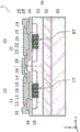
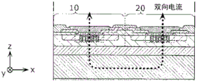
Fig. 1 is a cross-sectional view showing an example of the structure of a semiconductor device 1. Fig. 2A is a plan view thereof, and the size, shape, and arrangement of the electrode pads of the semiconductor device 1 are examples. Fig. 2B is a cross-sectional view schematically showing a main current flowing in the semiconductor device 1. FIGS. 1 and 2B are sectional views of section I-I in FIG. 2A.
As shown in fig. 1 and 2A, the semiconductor device 1 includes a semiconductor layer 40, a metal layer 30, A1 st vertical field effect transistor 10 (hereinafter also referred to as "transistor 10") formed in A1 st region A1 in the semiconductor layer 40, and A2 nd vertical field effect transistor 20 (hereinafter also referred to as "transistor 20") formed in A2 nd region A2 in the semiconductor layer 40. Here, as shown in fig. 2A, the 1 st region A1 and the 2 nd region A2 are adjacent to each other in a plan view (i.e., a top view) of the semiconductor layer 40. In fig. 2A, a virtual boundary 90C between the 1 st area A1 and the 2 nd area A2 is indicated by a broken line.
The semiconductor layer 40 is formed by laminating the semiconductor substrate 32 and the low-concentration impurity layer 33. The semiconductor substrate 32 is disposed on the back surface side of the semiconductor layer 40, and is made of silicon containing an impurity of the 1 st conductivity type. The low-concentration impurity layer 33 is disposed on the front surface side of the semiconductor layer 40, is formed in contact with the semiconductor substrate 32, and contains an impurity of the 1 st conductivity type at a concentration lower than that of the impurity of the 1 st conductivity type of the semiconductor substrate 32. The low-concentration impurity layer 33 may be formed on the semiconductor substrate 32 by epitaxial growth, for example. The low-concentration impurity layer 33 is also a drift layer of the transistor 10 and the transistor 20, and may be referred to as a drift layer in the present specification.
The metal layer 30 is formed in contact with the back surface side of the semiconductor layer 40, and is made of silver (Ag) or copper (Cu). The metal layer 30 may contain a trace amount of elements other than metals mixed as impurities in the production process of the metal material. The metal layer 30 may be formed on the entire back surface side of the semiconductor layer 40, or may not be formed on the entire back surface side of the semiconductor layer 40.
As shown in fig. 1 and 2A, in the 1 st region A1 of the low-concentration impurity layer 33, A1 st body (body) region 18 containing an impurity of a2 nd conductivity type different from the 1 st conductivity type is formed. In the 1 st body region 18, a1 st source region 14 containing an impurity of the 1 st conductivity type, a1 st gate conductor 15, and a1 st gate insulating film 16 are formed. The 1 st gate conductor 15 and the 1 st gate insulating film 16 are formed inside a plurality of 1 st trenches 17, respectively, the plurality of 1 st trenches 17 extending in a1 st direction (Y-axis direction) parallel to the upper surface of the semiconductor substrate 32 and being formed at equal intervals in a2 nd direction (X-direction) orthogonal to the 1 st direction (Y-direction) from the upper surface of the semiconductor layer 40 to a depth penetrating the 1 st body region 18 to a part of the low-concentration impurity layer 33. The 1 st source electrode 11 includes a portion 12 and a portion 13, and the portion 12 is connected to the 1 st source region 14 and the 1 st body region 18 via the portion 13. The 1 st gate conductor 15 is a buried gate electrode buried in the semiconductor layer 40, and is electrically connected to the 1 st gate electrode pad 119.
The portion 12 of the 1 st source electrode 11 is a layer to be bonded to a solder at the time of reflow in face down (face down) mounting, and may be formed of a metal material containing 1 or more of nickel, titanium, tungsten, and palladium, as an example of no limitation. The surface of the portion 12 may be plated with gold or the like.
The portion 13 of the 1 st source electrode 11 is a layer connecting the portion 12 and the semiconductor layer 40, and may be made of a metal material containing 1 or more of aluminum, copper, gold, and silver, as an example, though not limited thereto.
In the 2 nd region A2 of the low-concentration impurity layer 33, A2 nd body region 28 containing an impurity of the 2 nd conductivity type is formed. In the 2 nd body region 28, a2 nd source region 24 containing an impurity of the 1 st conductivity type, a2 nd gate conductor 25, and a2 nd gate insulating film 26 are formed. The 2 nd gate conductor 25 and the 2 nd gate insulating film 26 are formed inside a plurality of 2 nd trenches 27, respectively, and the plurality of 2 nd trenches 27 are formed from the upper surface of the semiconductor layer 40 to a depth penetrating the 2 nd body region 28 to a part of the low concentration impurity layer 33. The 2 nd source electrode 21 includes a portion 22 and a portion 23, and the portion 22 is connected to the 2 nd source region 24 and the 2 nd body region 28 via the portion 23. The 2 nd gate conductor 25 is an embedded gate electrode embedded in the semiconductor layer 40, and is electrically connected to the 2 nd gate electrode pad 129.
The portion 22 of the 2 nd source electrode 21 is a layer to be bonded to solder at the time of reflow in the face-down mounting, and may be formed of a metal material containing 1 or more of nickel, titanium, tungsten, and palladium, as an example of no limitation. The surface of the portion 22 may be plated with gold or the like.
The portion 23 of the 2 nd source electrode 21 is a layer connecting the portion 22 and the semiconductor layer 40, and may be made of a metal material containing 1 or more of aluminum, copper, gold, and silver, as an example of no limitation.
With the above-described structures of the transistor 10 and the transistor 20, the semiconductor substrate 32 functions as a common drain region in which the 1 st drain region of the transistor 10 and the 2 nd drain region of the transistor 20 are shared. A part of the low-concentration impurity layer 33 on the side contacting the semiconductor substrate 32 may also function as a common drain region. The metal layer 30 functions as a common drain electrode that is common to the drain electrode of the transistor 10 and the drain electrode of the transistor 20.
As shown in fig. 1, the 1 st body region 18 is covered with an interlayer insulating layer 34 having an opening, and a portion 13 of the 1 st source electrode 11 connected to the 1 st source region 14 through the opening of the interlayer insulating layer 34 is provided. The interlayer insulating layer 34 and the 1 st source electrode portion 13 are covered with a passivation layer 35 having an opening, and a portion 12 connected to the 1 st source electrode portion 13 through the opening of the passivation layer 35 is provided.
The 2 nd body region 28 is covered with an interlayer insulating layer 34 having an opening, and a portion 23 of the 2 nd source electrode 21 connected to the 2 nd source region 24 through the opening of the interlayer insulating layer 34 is provided. The interlayer insulating layer 34 and the 2 nd source electrode portion 23 are covered with a passivation layer 35 having an opening, and a portion 22 connected to the 2 nd source electrode portion 23 through the opening of the passivation layer 35 is provided.
Therefore, the plurality of 1 st source electrode pads 116 and the plurality of 2 nd source electrode pads 126 are regions where the 1 st source electrodes 11 and the 2 nd source electrodes 21 are partially exposed on the surface of the semiconductor device 1, respectively, so-called terminal portions. Similarly, the 1 st or more gate electrode pads 119 and the 1 or more gate electrode pads 129 are regions where the 1 st gate electrode 19 (not shown in fig. 1, 2A, and 2B) and the 2 nd gate electrode 29 (not shown in fig. 1, 2A, and 2B) are partially exposed on the surface of the semiconductor device 1, that is, portions of terminals, respectively.
In the semiconductor device 1, for example, the 1 st conductivity type may be an N-type, the 2 nd conductivity type may be a P-type, the 1 st source region 14, the 2 nd source region 24, the semiconductor substrate 32, and the low concentration impurity layer 33 may be N-type semiconductors, and the 1 st body region 18 and the 2 nd body region 28 may be P-type semiconductors.
In the semiconductor device 1, for example, the 1 st conductivity type may be P-type, the 2 nd conductivity type may be N-type, the 1 st source region 14, the 2 nd source region 24, the semiconductor substrate 32, and the low concentration impurity layer 33 may be P-type semiconductors, and the 1 st body region 18 and the 2 nd body region 28 may be N-type semiconductors.
In the following description, the on operation of the semiconductor device 1 will be described assuming that the transistors 10 and 20 are so-called N-channel transistors in which the 1 st conductivity type is an N-type and the 2 nd conductivity type is a P-type.
Note that, here, the description has been given on the assumption that the transistor 10 and the transistor 20 have symmetry without any difference in function, characteristics, structure, and the like. Fig. 1, 2A, and 2B are also drawn on the premise of symmetry, but in the chip-scale package type double-structure vertical field effect transistor of the present invention, symmetry is not necessarily a requirement.
[2. Orthogonal Structure ]
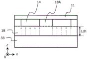
Fig. 3A and 3B are a plan view and a perspective view, respectively, of a substantial unit structure of the transistor 10 (or the transistor 20) repeatedly formed in the X direction and the Y direction in the semiconductor device 1. In fig. 3A and 3B, the semiconductor substrate 32 and the 1 st source electrode 11 (or the 2 nd source electrode 21) are not shown for easy understanding. The Y direction is a direction (1 st direction) parallel to the upper surface of the semiconductor layer 40 and extending from the 1 st trench 17 and the 2 nd trench 27. The X direction is a direction (2 nd direction) parallel to the upper surface of the semiconductor layer 40 and orthogonal to the Y direction.
As shown in fig. 3A and 3B, the transistor 10 includes a1 st connection portion 18A that electrically connects the 1 st body region 18 and the 1 st source electrode 11. The 1 st connection portion 18A is a region of the 1 st body region 18 where the 1 st source region 14 is not formed, and contains impurities of the same 2 nd conductivity type as the 1 st body region 18. The 1 st source region 14 and the 1 st connection 18A are alternately and periodically repeatedly arranged along the Y direction. The same applies to the transistor 20.
In the semiconductor device 1, if a high voltage is applied to the 1 st source electrode 11 and a low voltage is applied to the 2 nd source electrode 21, and a voltage equal to or higher than a threshold value is applied to the 2 nd gate electrode 29 (the 2 nd gate conductor 25) with reference to the 2 nd source electrode 21, a conduction channel is formed in the 2 nd body region 28 in the vicinity of the 2 nd gate insulating film 26. As a result, the main current flows through a path of the 1 st source electrode 11, the 1 st connection portion 18A, the 1 st body region 18, the low-concentration impurity layer 33, the semiconductor substrate 32, the metal layer 30, the semiconductor substrate 32, the low-concentration impurity layer 33, the conduction channel formed in the 2 nd body region 28, the 2 nd source region 24, and the 2 nd source electrode 21, and the semiconductor device 1 is brought into an on state. Further, a PN junction is present at the contact surface between the 2 nd body region 28 and the low-concentration impurity layer 33 in the conductive path, and functions as a body diode. Since the main current flows through the metal layer 30, the metal layer 30 is made thick, and the cross-sectional area of the main current path is enlarged, thereby reducing the on-resistance of the semiconductor device 1.
Similarly, in the semiconductor device 1, if a high voltage is applied to the 2 nd source electrode 21 and a low voltage is applied to the 1 st source electrode 11, and a voltage equal to or higher than a threshold value is applied to the 1 st gate electrode 19 (1 st gate conductor 15) with reference to the 1 st source electrode 11, an on channel is formed in the 1 st body region 18 in the vicinity of the 1 st gate insulating film 16. As a result, the main current flows through a path of the 2 nd source electrode 21, the 2 nd connecting portion 28A, the 2 nd body region 28, the low-concentration impurity layer 33, the semiconductor substrate 32, the metal layer 30, the semiconductor substrate 32, the low-concentration impurity layer 33, the conduction channel formed in the 1 st body region 18, the 1 st source region 14, and the 1 st source electrode 11, and the semiconductor device 1 is brought into an on state. In addition, a PN junction is present at a contact surface between the 1 st body region 18 and the low-concentration impurity layer 33 in the conduction path, and functions as a body diode.
Hereinafter, the length of the 1 st source region 14 in the Y direction is referred to as LS1, and the length of the 2 nd source region 24 in the Y direction is referred to as LS2. The length of the source region is referred to as LS when the 1 st source region 14 and the 2 nd source region 24 are not distinguished. The length of the 1 st connecting portion 18A in the Y direction is denoted as LB1, and the length of the 2 nd connecting portion 28A in the Y direction is denoted as LB2. The length of the connection portion is denoted as LB when the 1 st connection portion 18A and the 2 nd connection portion 28A are not distinguished.
The single-structure vertical field effect transistor is generally understood to be formed only on one side (the transistor 10) of the double-structure vertical field effect transistor. However, in the chip-size package type, it is necessary to provide a drain electrode pad on the front side of the semiconductor layer 40 including the 1 st source electrode pad 116 and the 1 st gate electrode pad 119. In this case, a drain lead structure electrically connected to the drain layer provided on the back surface side of the semiconductor layer 40 needs to be formed from the front surface side of the semiconductor layer 40.
[3. Base resistance in the orthogonal configuration ]
The transistor 10 (or the transistor 20) includes a parasitic bipolar transistor in structure. The parasitic bipolar transistor is easily turned on when the semiconductor device to be driven is turned off (turned off), i.e., the parasitic bipolar transistor is easily turned on as the driving voltage immediately before the semiconductor device is turned off is larger. When the semiconductor device 1 is turned off, the maximum driving voltage among the driving voltages at which the parasitic bipolar transistor is not turned on is referred to as off-time breakdown voltage (Voff) in the present invention. For example, it is known that when the parasitic bipolar transistor is off during 10V driving and is off during 11V driving, the breakdown voltage of the semiconductor device at the time of off is 10V or more and less than 11V. In the case where the semiconductor device 1 is a vertical field effect transistor of N conductivity type having a double structure, the drive voltage is a source-source Voltage (VSS), and in the case where the semiconductor device is a vertical field effect transistor having a single structure, the drive voltage is a drain-source Voltage (VDS). In the case where the semiconductor device 1 is a P-type vertical field effect transistor having a double structure, the driving voltage is a drain-drain Voltage (VDD). The drive means a state in which a voltage is applied to the gate conductor to conduct a current between the source and the source (or between the drain and the source, or between the drain and the drain), and means conduction in a linear region unless otherwise specified.
At least the semiconductor device 1 is required to have a breakdown voltage at the time of off that is equal to or higher than a standard maximum voltage between source and source (or a standard maximum voltage between drain and source, or a standard maximum voltage between drain and drain, or sometimes referred to as a standard maximum voltage without distinguishing them). The specification maximum voltage is a maximum rated voltage described in the product specification of the transistor. Whether a parasitic bipolar transistor is easily turned on is related to the base resistance Rb [ omega ] of the parasitic bipolar transistor. The base resistance Rb1[ Ω ] is an impedance (hereinafter referred to as "1 st impedance") at a position in the 1 st body region 18 where the impedance is the highest as viewed from the 1 st source electrode 11 in a path from the 1 st junction 18A to the 1 st body region 18, and the base resistance Rb2[ Ω ] is an impedance (hereinafter referred to as "2 nd impedance") at a position in the 2 nd body region 28 where the impedance is the highest as viewed from the 2 nd source electrode 21 in a path from the 2 nd junction 28A to the 2 nd body region 28.
If let the sheet resistivity (sheet resistivity) in the 1 st body region 18 (or the 2 nd body region 28) be ρ [ Ω · μm ], let the distance between the trenches be Lxm [ μm ], and let the distance (on-channel length) from the bottom of the 1 st source region 14 (or the 2 nd source region 24) to the boundary between the 1 st body region 18 (or the 2 nd body region 28) and the low-concentration impurity layer 33 be Lch [ μm ], then the base resistance Rb1 of the transistor 10 is expressed as Rb1= ρ × LS1/Lxm/Lch, and the base resistance Rb2 of the transistor 20 is expressed as Rb2= ρ × LS2/Lxm/Lch.
When the transistor 10 is turned off, the carriers accumulated in the vicinity of the 1 st gate insulating film 16 are instantaneously discharged to the 1 st source electrode 11 through the 1 st body region 18 and the 1 st connection portion 18A. At this time, if base resistance Rb1 is large, the voltage drop due to the passage of carriers also increases, and therefore the threshold at which the parasitic bipolar transistor is turned on is easily exceeded. The same applies to the transistor 20. Therefore, in order to increase the off-time breakdown voltage of the semiconductor device 1, rb1 and Rb2 need to be suppressed.
Further, if the distance Lxm between the trenches is reduced, the trenches can be further provided in the generated excess area, and therefore, the on-resistance can be reduced while the area of the semiconductor device 1 is kept constant. This is a measure for increasing the number of trenches and gate conductors (increasing the trench density) and increasing the total gate width of the semiconductor device 1. However, if the distance Lxm between the trenches is reduced as described above, rb increases, which causes a problem that the breakdown voltage at the time of off-state decreases.
If the surface resistivity ρ is considered to be constant, it is conceivable to shorten LS or lengthen Lch based on the above relational expression, regarding parameters that can be adjusted in a substituted manner so as not to increase Rb. However, the on-resistance is changed in the direction of increasing, and the effect of decreasing the on-resistance due to decreasing the distance Lxm between the trenches is offset. In such a relationship, it is difficult to achieve both a reduction in on-resistance and an improvement in the tolerance at the time of off-state.
Note that Lxm and Lxr are defined according to the position of the bottom-side portion of the 1 st source region 14 in the Z direction (the depth direction of the semiconductor device 1), which will be described later in embodiment 3. Based on the definition of the present invention, the symbols are correctly denoted as Lxmb [ μm ] and Lxrb [ μm ], but in embodiment 1, the symbols are Lxm and Lxr for the sake of simplicity.
[4. Conduction contribution of body region at the time of driving ]
The inventors of the present invention have found that, when driving the transistor 10, the 1 st body region 18 immediately below the 1 st connection portion 18A is efficiently made to contribute to conduction, and both reduction in on-resistance and improvement in tolerance at the time of turn-off are achieved. The description will be made with reference to FIGS. 4A to 4F and FIGS. 5A-1 to 5B-3.
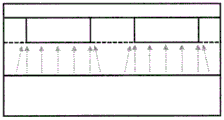
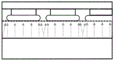
Fig. 4A, 4C, and 4E are schematic diagrams of cross sections obtained by cutting the vicinity of the 1 st trench 17 along the Y direction during driving of the transistor 10. Fig. 4B, 4D, and 4F are plan views illustrating the transistor 10 with the 1 st source electrode 11, the interlayer insulating layer 34, and the passivation layer 35 omitted. Fig. 4A schematically shows an energized state when VGS is small, assuming that a voltage applied to the 1 st gate conductor 15 (gate-source applied voltage) with reference to the potential of the 1 st source electrode 11 is VGS [ V ]. However, VGS exceeds the threshold because of the on state. The dashed arrows in the figure schematically indicate the flow of current through the inversion layer generated in the 1 st body region 18 as a conduction channel. This is shown in a plan view of the semiconductor layer 40, and is shown as a thick line portion in fig. 4B. Along the 1 st trench 17, the inversion layer generated just under the 1 st source region 14 contributes to conduction as a conduction channel.
In the 1 st body region 18 directly below the 1 st junction 18A, an inversion layer is formed in the vicinity of the 1 st trench 17, but since the 1 st junction 18A is directly above the 1 st source region 14, the inversion layer does not connect the drain region (low-concentration impurity layer 33) and the 1 st source region 14 in the Z direction, and does not form an on channel. However, in the Y direction, the inversion layer may contribute to conduction by connecting the drain region (low-concentration impurity layer 33) and the 1 st source region 14 obliquely only in a portion very close to the 1 st source region 14. The larger VGS, the larger the area contributing to conduction, the larger the area in the Y direction. Fig. 4C and 4D are schematic diagrams of the case where VGS is large, and the oblique dashed arrows in fig. 4C indicate the enlarged portions of the conducting regions. The enlargement of the conducting region can be understood in plan view as shown in fig. 4D. That is, the on region is slightly enlarged to both sides along the Y direction compared to the length of the 1 st source region 14.
When VGS is large, if the length LB1 of the 1 st connection portion 18A in the Y direction is made short, the 1 st source regions 14 on both sides approach each other, and therefore, the proportion of the region that can contribute to conduction to the inversion layer generated in the 1 st body region 18 directly below the 1 st connection portion 18A gradually increases from both sides, and becomes continuous from a certain point, and the entire length can effectively contribute as a conduction channel. Fig. 4E and 4F schematically show the situation at this time. If the 1 st body region 18 directly below the 1 st connection portion 18A is also included and conduction can be contributed along the entire length of the 1 st trench 17, a state that is very useful for reducing on-resistance is obtained. This is an effect obtained by shortening the length of the 1 st connection portion 18A, and is not an effect for relatively increasing the length of the 1 st source region 14.
Fig. 5A-1 to 5A-3 (hereinafter, simply referred to as "fig. 5A") and fig. 5B-1 to 5B-3 (hereinafter, simply referred to as "fig. 5B") show results of simulations on the condition that the 1 st body region 18 directly below the 1 st connection portion 18A contributes to conduction. Fig. 5A and 5B each show a cross section obtained by cutting the vicinity of the 1 st trench 17 of the transistor 10 along the Y direction, similarly to fig. 4A, 4C, and 4E. The upper section (FIGS. 5A-1, 5B-1) shows the configuration adopted in the simulation. The 1 st body region 18 is not divided by the 1 st source region 14 and the 1 st connecting portion 18A, but a boundary line is provided here for convenience. The middle section (fig. 5A-2 and 5B-2) shows the current density when conducting under the condition of large VGS by a dark and light, and the lower section (fig. 5A-3 and 5B-3) shows the upper section and the middle section overlapping each other.
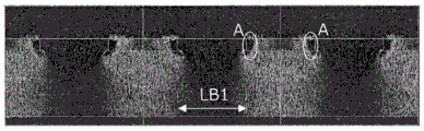
In both fig. 5A and 5B, the same value is applied to VGS, but in the structure shown in fig. 5A, since the length LB1 of the 1 st connection portion 18A is long (horizontal arrow in the figure), the 1 st body region 18 directly below the 1 st connection portion 18A hardly contributes to conduction. Only a limited portion of the current density is seen slightly near the 1 st source region 14. Further, as shown by a circle a in the figure, it can be confirmed that there is a portion where the current density becomes high at both ends of the 1 st source region 14 in the Y direction, and therefore, it is known that there is a current passing through the 1 st body region 18 directly below the 1 st connection portion 18A.
In contrast, in the structure shown in fig. 5B, since the length LB1 of the 1 st connection portion 18A is short (horizontal arrow in the figure), it is understood that most of the 1 st body region 18 directly below the 1 st connection portion 18A has a high current density to the same extent as that directly below the 1 st source region 14. This is because the length LB1 of the 1 st connection 18A is short, that is, the 1 st source regions 14 on both sides are close to each other, so that the divided conduction channels are connected to each other, and can contribute to conduction along the entire length of the 1 st trench 17. In fig. 5B, it can be seen that the current density is very high because the current passing through the 1 st body region 18 directly below the 1 st connecting portion 18A is concentrated at both ends of the 1 st source region 14 in the Y direction indicated by the circle B.
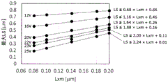
Fig. 6 shows an example of calculation of VGS dependency of the length in the Y direction of a conductive region extending from the 1 st source region 14 to the 1 st body region 18 directly below the 1 st connection portion 18A. The inventors of the present invention have performed calculations using a calculation model of a vertical field effect transistor of an N-conductivity type double structure matched with an actually measured value. The structure is of a cross type as shown in fig. 1 and fig. 3A to 3B, and the size (3.40 × 1.96 mm) of the semiconductor device, the width (Lxr =0.20 μm) of the inside of 1 trench, and other parameters are set to predetermined values. The length of the on region extending from only one side of the 1 st source region 14 in the Y direction is plotted on the vertical axis.
As can be seen from fig. 6, the larger VGS, the longer the enlarged conduction region. As an example, according to fig. 6, the enlargement of the on region when VGS =3.8V is 0.174 μm. Therefore, if the length LB1 of 1 st connection 18A sandwiched by the 1 st source regions 14 from both sides in the Y direction is 0.174 μm × 2=0.348 μm or less, the entire 1 st body region 18 directly below the 1 st connection 18A in the Y direction can be made to contribute to conduction. In other words, when LB1<0.35 μm, the full length in the Y direction contributes to conduction under the driving condition of VGS =3.8V or more.
If the size of VGS and the length LB1 of the 1 st connection portion 18A are appropriately selected, the on-resistance can be reduced by effectively forming an on-channel along the entire length of the 1 st trench 17 under desired driving conditions. This effect is obtained by setting the length LB1 of the 1 st connection portion 18A to a certain length or less, but at this time, the on-resistance is characterized by losing the dependency of the length LS1 of the 1 st source region 14. This is because the effective on channel is formed along the entire length of the 1 st trench, and thus the state during driving is the same regardless of whether the length LS1 of the 1 st source region 14 is long or short. In the semiconductor device 1 using a certain limited area, the length LB1 of the 1 st connection portion 18A cannot be changed alone, and if LB1 is made shorter, the total of the length LS1 of the 1 st source region 14 and the length LS1 of the 1 st source region 14 is normally increased. It is generally considered for those skilled in the art that the on-resistance decreases in the case of LS1 increase, but within the scope of the present invention, the on-resistance of transistor 10 does not decrease significantly even if the effect of LS1 increase is taken into account. Therefore, in the present invention, even if the length LB1 of the 1 st connection portion 18A is further shortened, it is characterized in that the on-resistance of the transistor 10 is not dependent on the length LS1 of the 1 st source region 14 but is in a convergence region that is not significantly reduced. Therefore, the length LS1 of the 1 st source region 14 can be shortened without deteriorating the on-resistance. Therefore, the reduction of base resistance Rb1 can be also achieved, which will be described later.
Tables 1 and 2 below are the results of calculation of the on-resistance at the time of driving at VGS =3.8V by the inventors of the present invention using the same calculation model as that used for deriving the calculation result of fig. 6. The distances Lxm between the trenches were set to 3 levels of 0.10 μm, 0.14 μm, and 0.18 μm, respectively. The trench inner width Lxr is fixed at 0.20 μm. In addition, driving at VGS =3.8V is a condition that the entire length along the Y direction can contribute to conduction if the length LB1 of the 1 st connection portion 18A is less than 0.35 μm as shown in fig. 6.
[ Table 1]

[ Table 2]

Table 1 shows the results of on-resistance when the length LB of the connection portion was changed while the length LS of the source region was fixed to 0.50 μm. When LB is long, the on-resistance is high, but if LB is made short, the total LS increases, and therefore the on-resistance may decrease. However, when LB <0.35 μm, the on-resistance is no longer reduced although the total LS increases.
Table 2 shows the results of on-resistance when the length LB of the connecting portion was fixed to 0.30 μm and the length LS of the source region was changed in contrast. If LS increases or decreases, the total LS also increases or decreases in a coordinated manner. However, under the condition that LB =0.30 μm is fixed, it is found that the on-resistance does not change depending on the increase or decrease of LS. This indicates that, since the full length in the Y direction can contribute to the on state already at the time of the driving with LB <0.35 μm and VGS =3.8V, a state is reached in which the on resistance is not affected regardless of the total size of LS or LS.
The results of table 1 and table 2 are plotted in fig. 7. The horizontal axis represents the ratio of LS to LB. Two levels of 0.18 μm and 0.10 μm are shown with respect to the trench-to-trench distance Lxm. It can be confirmed that the trends are the same although the absolute values of the on-resistances are different at the two levels. That is, the graph includes a rightward falling portion where the on-resistance decreases with an increase in LS/LB from left upward to right downward, and a fixed portion where there is no change in the on-resistance depending on the value of LS/LB. The rightward falling portion corresponds to table 1, and is the case when only LB is shortened (LS/LB is increased) while LS is maintained at 0.50 μm. In contrast, the fixed portion corresponds to table 2, and is the case when LS is only reduced (LS/LB is reduced) while LB is maintained at 0.30 μm. Since the condition of VGS =3.8V and LB <0.35 μm is present regardless of the value of Lxm, a fixed portion appears in the graph. That is, in the present invention, the on-resistance of the transistor 10 is in a convergence region in which the on-resistance does not significantly decrease even if the length LB1 of the 1 st connection portion 18A is further shortened, and means a state in which the on-resistance is not dependent on not only the length LB1 but also the length LS1 of the 1 st source region 14.
The on-resistance of the transistor 10 is an on-resistance when a voltage of a predetermined value or a current of a predetermined value is applied to the 1 st gate conductor 15. The specification is a product specification of the transistor, and fig. 8 shows an example of the on resistance (RSS (on) [ m Ω ]) described in the specification of the N-conductive type double-structure vertical field effect transistor. In the example of fig. 8, the voltage applied to the 1 st gate conductor 15 is VGS, and the specification value is one of 2.5V, 3.1V, 3.8V, and 4.5V, or an arbitrary value within the range. The current of the specification value IS the source-source current IS =6.9A.
The term "VGS is small" means that the vehicle is driven at a VGS lower than the minimum VGS specified by the specification. In the example of fig. 8, the condition is that the driving is performed at VGS <2.5V, which is higher than the threshold. The term "VGS is large" means that the vehicle is driven by VGS not less than the minimum VGS specified by the specification. In the example of fig. 8, the conditions are such that the driving is performed at VGS ≧ 2.5V. It is conceivable that the condition for actually using the transistor 10 is almost the condition that VGS is large. The specification in the above description is based on the characteristics at room temperature (mainly 25 ℃).
Therefore, in the present invention, even if the length LB1 of the 1 st connection portion 18A is further shortened, the on-resistance when a current of a value shown in the specification flows by driving with any VGS shown in the specification of the transistor 10 is in a convergence region where the on-resistance does not significantly decrease. In embodiment 1, LB <0.35 μm is shown as a condition that the entire length in the Y direction is an effective on channel, but VGS is not necessarily limited to 3.8V. When LB <0.35 μm, the effect of the present invention is obtained if the above-described feature is exhibited in driving under any VGS indicated by the product specification of the transistor.
[5. Compromise between decrease in on-resistance and improvement in tolerance at the time of off ]
By effectively utilizing the above-described effects, even if the length LS1 of the 1 st source region 14 is shortened in order to suppress the base resistance Rb1, if the length LB1 of the 1 st connecting portion 18A is shortened to a certain extent, the on-channel during driving can be effectively enlarged to reduce the on-resistance. Therefore, both the reduction of the on-resistance and the improvement of the tolerance at the time of off-state can be achieved.
Table 3 and fig. 9A to 9C below are diagrams showing a part of the results of calculations performed by the inventors of the present invention. When the distance Lxm between the trenches is shortened to reduce the on-resistance, the length LS1 of the 1 st source region 14 needs to be kept to a certain value or less to obtain a desired off-time breakdown voltage Voff. The maximum values of LS1 required to satisfy each Voff are shown in Table 3, and FIG. 9A is a graph obtained by plotting the values in the range of 0.08 μm ≦ Lxm ≦ 0.20. Mu.m.
[ Table 3]

In order to suppress the base resistance Rb1, it is known that there is a linear relationship between Lxm and the maximum length of the 1 st source region 14. This is caused by the relationship Rb1= ρ × LS 1/Lxm/Lch. For example, to make Voff exceed 22V, LS ≦ 0.51 μm is required when Lxm =0.18 μm. Similarly, LS ≦ 0.41 μm is required for Lxm =0.14 μm, and LS ≦ 0.36 μm is required for Lxm =0.10 μm. From the linear approximation of these plots, as shown in fig. 9A, the relationship of LS ≦ 1.88 × Lxm +0.16[ μm ] may be satisfied. Similarly, a linear relationship can be obtained between Lxm and maximum LS to satisfy each Voff, and the maximum LS is limited as Lxm is shortened as desired as Voff is larger.
In the linear relationship between Lxm and the maximum LS, which is established in order to satisfy the desired Voff, at least in the range of 12V to 25V, the slope and the intercept continuously change as shown in fig. 9B and 9C, respectively. Therefore, if LS that must be satisfied in accordance with the change in Lxm is applied to the relational expression in consideration of the dependency of Voff, the relationship LS ≦ 0.12 × Voff × Lxm-0.76 × lxxm-0.05 × Voff +1.26[ μm ] may be satisfied. In a field effect transistor, normally, the breakdown voltage at the time of off is required to be equal to or higher than the specification maximum voltage. Therefore, if the specification maximum voltage is Vss [ V ], the relationship LS ≦ 0.12 × Vss × Lxm-0.76 × Lxm-0.05 × Vss +1.26[ μm ] is preferably satisfied. At this time, if a relationship of LB <0.35 μm is established with respect to the length LB of the connection portion at the same time, the total length along the Y direction contributes to conduction, and thus the reduction of the on resistance can be also achieved.
In the present invention, it is the first significance to shorten Lxm and increase the trench density for the purpose of reducing the on-resistance. In the present invention, the distance Lxm between the trenches is at least the internal width Lxr of the trenches (Lxm ≦ Lxr), and a region where Lxr ≦ 0.20 μm is considered as a study target. The calculations in tables 1 and 2 were calculated with the result that Lxr =0.20 μm being fixed. However, the results in table 3 and fig. 9A are determined independently of the value of Lxr. This is because Lxm determines the base resistance Rb, and Lxr does not affect it. Therefore, the results in Table 3 and FIG. 9A can be considered to be generally valid under the premise of the present invention that Lxm ≦ Lxr ≦ 0.20 μm.
Fig. 10 shows a relationship between LS and LB that is desirable for obtaining the effects of the semiconductor device 1 of the present invention, based on the calculation results in table 3 and the range in fig. 9A, in a case where Lxr =0.20 μm and Voff is 22V, as an example, from a relationship between Lxm and Lxr. The value is the maximum value of LS and LB that can obtain the effect of the semiconductor device 1 of the present invention when Lxm ≦ Lxr, and LS =0.54 μm and LB =0.35 μm in this case. LS =0.54 μm is a value calculated from Lxm = Lxr =0.20 μm according to the relational expression of fig. 9A when Voff is 22V. Therefore, when the relationship of Lxm ≦ Lxr is satisfied, the ranges LS ≦ 0.54 μm and LB <0.35 μm are sufficient. Δ is the maximum value of LS and LB that can obtain the effect of the semiconductor device 1 of the present invention when Lxm ≦ Lxr/2, where LS =0.35 μm and LB =0.35 μm. LS =0.35 μm is a value calculated from Lxm = Lxr/2=0.10 μm from the relational expression of fig. 9A when Voff is 22V. Therefore, when Lxm ≦ Lxr/2, LS ≦ 0.35 μm and LB <0.35 μm may be satisfied. The physical characteristics when Lxm is Lxr/2 or less will be described in embodiment 2.
As described above, in the semiconductor device 1 according to embodiment 1, in the 1 st vertical field effect transistor 10 in which the 1 st source region 14 and the 1 st connection part 18A connecting the 1 st body region 18 and the 1 st source electrode 11 are alternately and periodically provided in the 1 st direction (Y direction) in which the 1 st trench 17 extends, in the 2 nd direction (X direction) orthogonal to the 1 st direction (Y direction), the distance Lxm between the adjacent trench 17 and the internal width Lxr of the trench 17 are in the relationship of Lxm ≦ Lxr ≦ 0.20 μm, and with respect to the length of the 1 st connection part 18A, the on-resistance of the 1 st vertical field effect transistor 10 when a prescribed value of current is applied to the 1 st gate conductor 15 at a prescribed value is in a convergence region where the length of the 1 st connection part 18A does not significantly decrease even if the length of the 1 st connection part 18A is further shortened. The same applies to the 2 nd vertical field effect transistor 20.
This feature provides a semiconductor device that can achieve both a reduction in on-resistance and an improvement in the tolerance during turn-off. That is, both reduction in on-resistance and improvement in the tolerance at the time of off-state can be achieved, and the circuit specification of high withstand voltage and low resistance which has been demanded in recent years can be easily realized.
(embodiment mode 2)
In embodiment 1 and fig. 5, it is described that the total length along the Y direction of the 1 st groove 17 can be made to contribute to conduction by controlling the length LB1 of the 1 st connection portion 18A. The same effect can be expected in the X direction. This is nothing more than replacing the 1 st connecting portion 18A in the Y direction by the distance Lxm between the 1 st groove 17 and the adjacent other 1 st groove 17 in the X direction.
If VGS becomes equal to or higher than the threshold value, an inversion layer is generated in the 1 st body region 18 in the vicinity of the 1 st trench 17, but as VGS increases, the inversion layer expands in the X direction and increases in thickness. At this time, if Lxm is short, the inversion layers formed in the 1 st trenches 17 adjacent to each other are connected, and there is a possibility that the 1 st body regions 18 may all contribute to conduction in the X direction. This operation is the same as the case where the 1 st connection part 18A is effectively utilized as the conduction region in embodiment 1. Therefore, if the relation Lxm ≦ LB is also satisfied in the driving condition for causing the entire length along the Y direction of the 1 st trench 17 to contribute to conduction, the entire length along the X direction may contribute to conduction except for the inside of the 1 st trench 17, and the on resistance may be reduced.
In order to effectively use an inversion layer connected in the X direction as an on channel in a region between the 1 st trench 17 and another adjacent 1 st trench 17, it is preferable to provide the 1 st source region 14 directly above the 1 st body region 18 at an arbitrary position along the 2 nd direction. That is, it is required to form an on channel from the drain region (low-concentration impurity layer 33) to the 1 st source region 14 in a path as short as possible. That is, it is preferable that the 1 st source region 14 does not include a region locally formed to be shallow in the Z direction at a position between the 1 st trench 17 and another 1 st trench 17 adjacent to each other in the 2 nd direction.
Thus, the following configuration is preferable: the distance Lxm [ μm ] between the 1 st trench 17 and the 1 st trench 17 adjacent to each other in the 2 nd direction is equal to or less than the length LB [ μm ] of the 1 st connection 18A in the 1 st direction, and a plurality of layers having different conductivity types are not alternately provided when a region from the 1 st trench 17 to another adjacent 1 st trench 17 is observed along the 2 nd direction at any position in the 3 rd direction (Z direction) orthogonal to the 1 st direction and the 2 nd direction in the 1 st direction. With such a structure, the on-resistance can be reduced by obtaining a large conduction region in both the 1 st direction (Y direction) and the 2 nd direction (X direction) during driving.
Structurally, the inside of the 1 st trench 17 does not contribute to conduction in any way, and it is preferable to make it as short as possible, for example, it is preferable to set Lxr ≦ 0.20 μm. For this reason, the 1 st groove 17 is preferably in a shape of: the sidewalls are formed as vertically as possible without taper in the depth direction. Further, shortening Lxm is also effective because inversion layers formed in the vicinity of the 1 st trench 17 on both sides when driven in the X direction are easily connected. As 1 criterion, lxm ≦ Lxr/2 is preferred. In this case, the X direction can be effectively used for conduction even under lower VGS driving than when Lxr/2 yarn-woven fabric layer lxm ≦ Lxr, which can bring about an effect of reducing on-resistance more effectively. That is, the condition that VGS can be large can be expanded to the low VGS side, and the degree of freedom in the manner of using the semiconductor device 1 can be expanded. Fig. 10 shows an example of a preferable range of the length of the 1 st source region 14 and the length of the 1 st connecting portion 18A in the Y direction when Lxm ≦ Lxr/2, where Voff is 22V.
(embodiment mode 3)
The structure of the 1 st source region 14 (or the 2 nd source region 24) can be appropriately changed in the Z direction (depth direction of the semiconductor device) according to the function thereof. As shown in fig. 11A and 11B, the 1 st source region 14 may be formed separately in the Z direction by providing an upper portion 141 located on the upper surface side of the semiconductor layer 40 and a bottom portion 142 located on the boundary side with the 1 st body region 18.
The items on the upper side are denoted by t, and the items on the bottom side are denoted by b. The length LS1[ μm ] of the 1 st source region 14 is LSt1[ μm ] in the upper side portion 141 and LSb1[ μm ] in the bottom side portion 142. Similarly, the length LB1[ mu ] m of the connection part 1A is LBt1[ mu ] m on the upper side and LBb1[ mu ] m on the bottom side. Although not shown, the distance Lxm between the trenches and the inner width Lxr of the trenches are also set to Lxmb [ μm ] and Lxrb [ μm ] respectively, which are defined by the same depth as the bottom portion 142 of the 1 st source region 14.
As described in embodiment 1, in order to effectively utilize the 1 st body region 18 along the entire length of the 1 st trench 17 as a conduction channel while including the 1 st body region 18 during driving of the transistor 10, the length LB1 of the 1 st connection portion 18A needs to be shortened to a constant length or less. In this case, in the 1 st connecting portion 18A, the length LBb1 on the bottom side near the boundary with the 1 st body region 18 needs to be shortened to a certain length or less, and the length LBt1 on the upper side does not need to be uniformly shortened. This is because, as shown in fig. 4C and 4E, the on channel expands radially in the YZ plane from the bottom side of the 1 st source region 14 during driving.
Therefore, as for the 1 st source region 14, the length LSb1 of the bottom side portion 142 may be relatively long, and the length LSt1 of the upper side portion 141 may be relatively short. This is the same as making the bottom-side length LBb1 relatively short and the upper-side length LBt1 relatively long in the 1 st link 18A.
In embodiment 1 (fig. 4A), it is assumed that the length LS1 of the 1 st source region 14 is substantially constant in the Z direction. In embodiment 3 (fig. 11A), the length of the upper side portion 141 may be constant, but the length of the bottom side portion 142 may vary. The length LSb1 of the bottom side portion 142 is the length in the Z direction at which the Y direction length of the bottom side portion 142 is the largest. LSb1 is preferably longer than the length LSt1 of the upper portion 141, in order to efficiently expand the conductive region in the Y direction even when the amount is small during driving as described above. In order to obtain this effect, the length LSb1 of the bottom portion 142 may be defined to be located closer to the bottom than the center of the 1 st source region 14 in the Z direction, and more preferably, the bottommost position of the 1 st source region 14 in the Z direction.
That is, in the 3 rd direction (Z direction) orthogonal to the 1 st direction (Y direction) and the 2 nd direction (X direction), the 1 st source region 14 has an upper side portion 141 having a constant length in the 1 st direction and located on the upper surface side of the semiconductor layer 40, and a bottom side portion 142 having a variable length in the 1 st direction and located on the boundary side with the 1 st body region 18, and when the length of the upper side portion 141 in the 1 st direction is an upper source length LSt1 and the length of the bottom side portion 142 in the 1 st direction is the bottom source length LSb1, the bottom source length LSb1 is provided on the bottom side of the center in the 3 rd direction of the 1 st source region 14, and the bottom source length LSb1 is longer than the upper source length LSt1 (LSt 1< LSb 1), and the length of the 1 st source region 14 may be defined (that is, may be uniform) based on the bottom source length LSb1 (LS 1= LSb 1).
In embodiment 1 or embodiment 2 of the present invention, the length LS1 in the Z direction of the 1 st source region 14 does not need to be constant, and the 1 st source region 14 may be configured by the upper side portion 141 and the bottom side portion 142. In such a case, in the contents described in embodiment 1 or embodiment 2, the parts denoted by LS1 and LB1 (LS 2 and LB 2) may be referred to as LSb1 and LBb1 (LSb 2 and LBb 2), respectively.
Embodiment 1 (fig. 4E) is compared with embodiment 3 (fig. 11C) again. The length of the 1 st source region 14 in embodiment 3 (fig. 11C) is the same as the length of LS1 on the bottom side in embodiment 1 (fig. 4E) (LS 1= LSb 1). Therefore, the width of the on channel is the same between the two independent of the magnitude of VGS, and no significant difference in on characteristics occurs.
However, in embodiment 3 (fig. 11A), LSt1 is short, and therefore the length LBt1 on the upper side of the 1 st link 18A is longer than that in embodiment 1. Such a structure is suitable for increasing the amount of P-conductive impurity implantation into the 1 st connection portion 18A and reducing the contact resistance between the 1 st body region 18 and the 1 st source electrode 11. This is because, when the length LS in the Y direction of the 1 st source region 14 adjacent to each other is intended to be long, the amount of P conductive impurity implanted into the 1 st connection portion 18A needs to be suppressed. Therefore, if the structure is originally short in LSt1, the amount of P conductive type impurity implanted into the adjacent 1 st connecting portion 18A can be increased, and therefore, the contact resistance between the 1 st body region 18 and the 1 st source electrode 11 can be easily reduced. In addition, when the transistor 10 is turned off, in a process in which the carriers accumulated in the vicinity of the 1 st gate insulating film 16 pass through the 1 st body region 18 and the 1 st connection 18A and are instantaneously discharged to the 1 st source electrode 11, the length of the upper portion side of the 1 st connection 18A is longer than that of embodiment 1 (LB 1< LBt 1). Therefore, base resistance Rb1 is reduced in accordance with the amount of phase difference, and the effect of improving the tolerance at the time of turn-off is obtained.
The present invention is to effectively expand the on channel during driving along the entire length of the 1 st trench 17, but for this purpose, the length of the 1 st connection 18A needs to be reduced to a constant length or less. Shortening is a control to a length of less than 0.50 μm, and if the length of the 1 st connection portion 18A is excessively shortened due to variations in manufacturing or the like, there is a possibility that the function of the 1 st connection portion 18A is degraded at the time of cutoff. However, in embodiment 3, since LBt1 can be simply made longer, margin for variation in manufacturing is increased, and the function of the 1 st connection part 18A at the time of off-state is stably obtained, and on-state characteristics at the time of driving are not impaired.
Fig. 11A shows an example of a structure in which the length LSb1 of the bottom portion 142 is relatively long and the length LSt1 of the upper portion 141 is relatively short in the 1 st source region 14. Although not limited to the example shown here, the Y-direction length of the upper portion 141 is substantially constant at any position in the Z-direction, whereas the Y-direction length of the bottom portion 142 varies in the Z-direction. As shown in fig. 11A, the bottom side portion 142 has a shape such that: the length in the Y direction is the largest at any position on the bottom side of the 1 st source region 14 in the Z direction. Alternatively, as shown in fig. 11D, the shape may be such that: the length in the Y direction is longest at the bottommost portion that is the boundary with the 1 st body region 18, and the length monotonically decreases as the upper portion side portion 141 approaches.
The length LSb1 of the bottom side portion 142 is preferably longer symmetrically to both sides in the Y direction than the length LSt1 of the upper side portion 141. That is, the center positions of the upper side portion 141 and the bottom side portion 142 of the 1 st source region 14 in the 1 st direction may be the same. With such a shape, the conductive regions radially extending from the 1 st source region 14 adjacent to the 1 st body region 18 in the Y direction are also symmetrical, and the 1 st body region 18 can be used as an effective conduction channel during driving, so that the contribution from the adjacent 1 st source region 14 can be obtained uniformly.
Further, the bottom portion 142 may be equally long by about 0.05 μm on both sides in the Y direction with respect to the upper portion 141. That is, LSt1< LSb1, more preferably in the relationship of LSb1 ≦ LSt1+0.10[ μm ]. With such a shape, even if variations in manufacturing are added, it is possible to prevent the function of the 1 st connection portion 18A from being degraded when the adjacent 1 st source regions 14 are excessively close to each other and are disconnected.
In embodiment 3 (fig. 11A), LSt1 is shorter, so that the ratio of the length of the 1 st source region 14 in the Y direction (strictly, the length of the upper side portion 141) to the length of the 1 st connection 18A (strictly, the length of the upper side portion) in the planar view of the structure is different from the ratio of the lengths of the bottom side portions. As described above, in order to improve the on-characteristics, it is preferable to make the source region longer on the bottom side (the connection portion is shorter), and in order to improve the tolerance at the time of off, it is preferable to make the connection portion longer on the upper side (the source region is shorter). Therefore, it is preferable to control so that ≧ LBb1 on the bottom side LSb1 and < LBt1 on the upper side LSt 1. In other words, the ratio of the length of the 1 st source region 14 on the upper side to the length of the 1 st connection portion 18A may be less than 1 (LSt 1/LBt1< 1), and the ratio of the length of the 1 st source region 14 on the bottom side to the length of the 1 st connection portion 18A may be 1 or more (LSb 1/LBt1 ≧ 1). In addition, in order to achieve compatibility with the relationship of LSb1 ≈ LSt1+0.10[ μm ], it is more preferable that LBt1-LSt1 ≦ 0.20[ μm ].
Further, although fig. 5B shows a case where a portion (circle frame B) where the current is concentrated appears at both ends of the 1 st source region 14 in the Y direction, if the length of the upper portion 141 of the 1 st source region 14 is made short (LSt 1< LSb 1), the current is more likely to be concentrated, and the upper portion 141 may become a cause of an increase in on-resistance during driving. In order to prevent this, the N conductivity type impurity concentration may be increased in the upper portion 141 compared to the bottom portion 142, thereby reducing the on-resistance. That is, the impurity concentration of the upper side portion 141 of the 1 st source region 14 may be higher than the impurity concentration of the bottom side portion 142.
As shown in fig. 11A or 11D, the 1 st source region 14 is manufactured by various methods to have a structure of LSt1< LSb 1. For example, first, in the N-conductivity type impurity implantation into the 1 st source region 14, the implantation is performed with a high acceleration energy into the bottom portion 142, and then the impurity implantation into the upper portion 141 is performed with changing the conditions. If the acceleration energy is relatively low compared to the condition toward the bottom portion 142 toward the upper portion 141, the impurity remains only in the shallow portion (upper portion) and can be relatively expanded in the Y direction with respect to the bottom portion 142 to diffuse the implanted impurity.
After the impurity implantation into the 1 st source region 14, the progress of the impurity diffusion in the Y direction in the bottom portion 142 may be utilized by performing a heat treatment such as annealing. Further, the following manufacturing method may be used: after the 1 st source region 14 is formed temporarily, P-conductive type impurities are implanted shallowly only in a certain region defined in the Y direction where the 1 st connection portion 18A is formed, and finally the bottom side portion 142 of the 1 st source region 14 is formed.
Various methods are available for measuring the dimension of the length LS1 of the 1 st source region, and an example will be described below. First, the transistor 10 is cut in the Y direction parallel to the 1 st trench 17, and a certain range in the cross section is measured by a Scanning Capacitance microscope (SCM = Scanning Capacitance microscope). Although it is difficult for the SCM to measure the impurity concentration of the semiconductor on the observation surface, the SCM can measure the conductivity type with high accuracy, and therefore the conductivity type of the semiconductor in the cross section can be plotted. According to SCM, the difference in N-type and P-type is generally expressed by a capacitance variation depending on the carrier concentration, and numerical data indicating the signal intensity of the polarity in absolute value is obtained for each unit portion to be measured. A certain range for performing the SCM measurement is selected so that the 1 st source region 14 and the 1 st connection 18A are alternately included a plurality of times.
Then, by comprehensively grasping the obtained numerical data, the position in the Z direction at which the length of the 1 st source region 14 in the Y direction is considered to be the maximum or near the maximum is identified. If the numerical data in the Y direction at the Z position is plotted, a distribution diagram is obtained in which the horizontal axis represents the position in the Y direction and the vertical axis represents the signal intensity of the conductivity type and the polarity. Since a place where the vertical axis is 0 can be interpreted as a position corresponding to the boundary between the N-type and the P-type, a place where the vertical axis alternately becomes 0 can be considered as a place where the boundary between the 1 st source region 14 and the 1 st connection 18A alternately appears. Therefore, the lengths LS and LB can be measured for each 1 st source region 14 or each 1 st connection portion 18A included in a certain measured range. If the 1 st source region 14 and the 1 st connection portion 18A are included in a certain range, LS and LB are determined to be appropriate based on the average values thereof.
The semiconductor device of the present invention has been described above based on embodiments 1 to 3, but the present invention is not limited to these embodiments. Various modifications of the embodiments, or other embodiments constructed by combining some of the constituent elements of the embodiments, which will occur to those skilled in the art, are also included in the scope of the present invention, unless they depart from the spirit of the present invention.
Industrial applicability
A semiconductor device including the vertical field effect transistor of the present invention can be widely used as a device for controlling the on state of a current path.
Description of the reference symbols
1. Semiconductor device with a plurality of semiconductor chips
10. Transistor (No. 1 vertical field effect transistor)
11. 1 st source electrode
12. Section 13
14. 1 st source region
15. 1 st gate conductor
16. 1 st gate insulating film
17. 1 st trench
18. 1 st body region
19. 1 st gate electrode
20. Transistor (No. 2 vertical field effect transistor)
21. 2 nd source electrode
22. Section 23
24. 2 nd source region
25. 2 nd gate conductor
26. 2 nd gate insulating film
27. 2 nd trench
28. 2 nd body region
28A No. 2 connection part
29. 2 nd gate electrode
30. Metal layer
32. Semiconductor substrate
33. Low concentration impurity layer or drift layer
34. Interlayer insulating layer
35. Passivation layer
40. Semiconductor layer
90C boundary
116. No. 1 source electrode pad
119. No. 1 gate electrode pad
126. 2 nd source electrode pad
129. 2 nd gate electrode pad
141. Upper side part
142. Bottom side part
Claims (10)
1. A semiconductor device of a chip size package type which can be mounted face down, characterized in that,
the vertical field effect transistor includes:
a semiconductor substrate made of silicon and containing an impurity of a1 st conductivity type;
a low-concentration impurity layer formed in contact with the semiconductor substrate and containing the impurity of the 1 st conductivity type at a concentration lower than that of the impurity of the 1 st conductivity type in the semiconductor substrate;
a body region of a2 nd conductivity type different from the 1 st conductivity type formed on a surface of the low-concentration impurity layer;
a source region of the 1 st conductivity type formed on a surface of the body region;
a source electrode electrically connected to the source region;
a plurality of trenches extending in a1 st direction parallel to an upper surface of the semiconductor substrate and formed at equal intervals in a2 nd direction orthogonal to the 1 st direction from the upper surface of the low-concentration impurity layer to a depth penetrating the body region to a part of the low-concentration impurity layer;
a gate insulating film formed to cover at least a part of the surfaces of the plurality of trenches;
a gate conductor formed on the gate insulating film; and
a connection portion electrically connecting the body region and the source electrode;
in the vertical field effect transistor, the source region and the connection portion are alternately and periodically provided in the 1 st direction;
when the distance between the adjacent trenches in the 2 nd direction is Lxm [ mu ] m and the internal width of 1 trench is Lxr [ mu ] m,
lxm ≦ Lxr ≦ 0.20 μm holds;
when the maximum voltage of the vertical field effect transistor is set to Vss,
a length LS [ μm ] of 1 of the source regions in the 1 st direction and a length LB [ μm ] of 1 of the connection portions in the 1 st direction are in the following relationship:
LB <0.35 μm, and,
LS≦0.12×Vss×Lxm-0.76×Lxm-0.05×Vss+1.26[μm]。
2. the semiconductor device according to claim 1,
a distance Lxm [ μm ] between the trenches adjacent to each other in the 2 nd direction is equal to or less than a length LB [ μm ] of the connection portion in the 1 st direction;
when a region from the trench to another adjacent trench is viewed in the 2 nd direction at any position in the 1 st direction, the region is not alternately provided with a plurality of layers having different conductivity types when viewed in the 2 rd direction at any position in the 3 rd direction orthogonal to the 1 st direction and the 2 nd direction.
3. The semiconductor device according to claim 2,
with respect to the length of the connection portion of the vertical field effect transistor in the 1 st direction, the on-resistance of the vertical field effect transistor when a voltage of a predetermined value is applied to the gate conductor and a current of a predetermined value flows through the vertical field effect transistor is in a convergence region where the length of the connection portion is not significantly reduced even when the length of the connection portion is further shortened.
4. The semiconductor device according to claim 2,
lxm ≦ Lxr/2 holds.
5. The semiconductor device according to claim 1,
in the 3 rd direction orthogonal to the 1 st direction and the 2 nd direction,
the source region has an upper portion side portion located on an upper surface side of the low-concentration impurity layer and having a constant length in the 1 st direction, and a bottom portion side portion located on a boundary side with the body region and having a variable length in the 1 st direction;
assuming that the length of the upper portion in the 1 st direction is an upper source length and the maximum length of the bottom portion in the 1 st direction is a bottom source length,
the bottom source length is a length of the bottom portion side portion on the bottom side from the center of the source region in the 3 rd direction;
the bottom source length is longer than the upper source length, and the length of the source region is equal to the bottom source length.
6. The semiconductor device according to claim 5,
the upper portion and the bottom portion of 1 of the source regions are located at the same position in the center in the 1 st direction.
7. The semiconductor device according to claim 5,
the ratio of the length of 1 of the source regions to the length of 1 of the connecting portions in the 1 st direction is less than 1 on the upper side and 1 or more on the bottom side.
8. The semiconductor device according to claim 7,
on the side of the above-mentioned upper portion,
the difference between the length of 1 of the source regions and the length of 1 of the connection portions in the 1 st direction is 0.20 μm or less.
9. The semiconductor device according to claim 5,
the impurity concentration of the upper portion side of the source region is higher than the impurity concentration of the bottom portion side of the source region.
10. A semiconductor device of a chip size package type which can be mounted face down, characterized in that,
the vertical field effect transistor includes:
a semiconductor substrate made of silicon and containing an impurity of a1 st conductivity type;
a low-concentration impurity layer formed in contact with the semiconductor substrate and containing an impurity of the 1 st conductivity type at a concentration lower than that of the impurity of the 1 st conductivity type in the semiconductor substrate;
a body region of a2 nd conductivity type different from the 1 st conductivity type formed on a surface of the low-concentration impurity layer;
a source region of the 1 st conductivity type formed on a surface of the body region;
a source electrode electrically connected to the source region;
a plurality of trenches extending in a1 st direction parallel to the upper surface of the semiconductor substrate and formed at equal intervals in a2 nd direction orthogonal to the 1 st direction from the upper surface of the low concentration impurity layer to a depth penetrating the body region to a part of the low concentration impurity layer;
a gate insulating film formed to cover at least a part of the surfaces of the plurality of trenches;
a gate conductor formed on the gate insulating film; and
a connection portion electrically connecting the body region and the source electrode;
in the vertical field effect transistor, the source region and the connection portion are alternately and periodically provided in the 1 st direction;
when the distance between the adjacent trenches in the 2 nd direction is Lxm [ mu ] m and the internal width of 1 trench is Lxr [ mu ] m,
lxm ≦ Lxr ≦ 0.20 μm holds;
when the maximum voltage of the vertical field effect transistor is set to Vss,
a length LS [ μm ] of 1 of the source regions in the 1 st direction and a length LB [ μm ] of 1 of the connection portions in the 1 st direction are in the following relationship:
LB <0.30 μm, and,
LS≦0.12×Vss×Lxm-0.76×Lxm-0.05×Vss+1.26[μm]。
Applications Claiming Priority (1)
| Application Number | Priority Date | Filing Date | Title |
|---|---|---|---|
| PCT/JP2021/034220 WO2023042359A1 (en) | 2021-09-17 | 2021-09-17 | Semiconductor device |
Publications (2)
| Publication Number | Publication Date |
|---|---|
| CN115152032A CN115152032A (en) | 2022-10-04 |
| CN115152032B true CN115152032B (en) | 2023-03-14 |
Family
ID=82748809
Family Applications (1)
| Application Number | Title | Priority Date | Filing Date |
|---|---|---|---|
| CN202180008223.0A Active CN115152032B (en) | 2021-09-17 | 2021-09-17 | Semiconductor device with a plurality of semiconductor chips |
Country Status (5)
| Country | Link |
|---|---|
| US (1) | US11637176B2 (en) |
| JP (1) | JP7114824B1 (en) |
| KR (1) | KR102434890B1 (en) |
| CN (1) | CN115152032B (en) |
| WO (1) | WO2023042359A1 (en) |
Families Citing this family (1)
| Publication number | Priority date | Publication date | Assignee | Title |
|---|---|---|---|---|
| JP2022092731A (en) * | 2020-12-11 | 2022-06-23 | 株式会社東芝 | Semiconductor device |
Citations (9)
| Publication number | Priority date | Publication date | Assignee | Title |
|---|---|---|---|---|
| JP2008159601A (en) * | 2005-11-28 | 2008-07-10 | Fuji Electric Device Technology Co Ltd | Semiconductor device and manufacturing method thereof |
| CN101645459A (en) * | 2008-08-08 | 2010-02-10 | 索尼株式会社 | Semiconductor device and method of manufacturing the same |
| CN103489864A (en) * | 2012-06-13 | 2014-01-01 | 株式会社东芝 | Power semiconductor device |
| JP2016171341A (en) * | 2016-05-26 | 2016-09-23 | ローム株式会社 | Semiconductor device |
| WO2018123799A1 (en) * | 2016-12-27 | 2018-07-05 | パナソニックIpマネジメント株式会社 | Semiconductor device |
| JP2018152504A (en) * | 2017-03-14 | 2018-09-27 | エイブリック株式会社 | Semiconductor device |
| JP2019201217A (en) * | 2014-04-15 | 2019-11-21 | ローム株式会社 | Semiconductor device and method of manufacturing semiconductor device |
| CN111133588A (en) * | 2017-09-18 | 2020-05-08 | 株式会社电装 | Semiconductor device and method for manufacturing the same |
| JP2020141130A (en) * | 2019-02-27 | 2020-09-03 | 株式会社デンソー | Silicon carbide semiconductor device and manufacturing method of the same |
Family Cites Families (16)
| Publication number | Priority date | Publication date | Assignee | Title |
|---|---|---|---|---|
| JPH05304297A (en) | 1992-01-29 | 1993-11-16 | Nec Corp | Semiconductor power device and manufacture thereof |
| JP4194890B2 (en) * | 2003-06-24 | 2008-12-10 | 株式会社豊田中央研究所 | Semiconductor device and manufacturing method thereof |
| JP3999225B2 (en) | 2004-01-27 | 2007-10-31 | 松下電器産業株式会社 | Semiconductor device and manufacturing method thereof |
| US7372088B2 (en) | 2004-01-27 | 2008-05-13 | Matsushita Electric Industrial Co., Ltd. | Vertical gate semiconductor device and method for fabricating the same |
| DE102005014743B4 (en) | 2005-03-31 | 2013-12-05 | Infineon Technologies Austria Ag | MOS field plate trench transistor means |
| JP5285242B2 (en) * | 2007-07-04 | 2013-09-11 | ローム株式会社 | Semiconductor device |
| JP2009302510A (en) * | 2008-03-03 | 2009-12-24 | Fuji Electric Device Technology Co Ltd | Trench gate type semiconductor device, and method of manufacturing the same |
| JP2013197122A (en) * | 2012-03-15 | 2013-09-30 | Toshiba Corp | Semiconductor device |
| US10608104B2 (en) | 2014-03-28 | 2020-03-31 | Infineon Technologies Ag | Trench transistor device |
| JP6566512B2 (en) | 2014-04-15 | 2019-08-28 | ローム株式会社 | Semiconductor device and manufacturing method of semiconductor device |
| JP6369173B2 (en) * | 2014-04-17 | 2018-08-08 | 富士電機株式会社 | Vertical semiconductor device and manufacturing method thereof |
| DE102014114832B4 (en) * | 2014-10-13 | 2020-06-18 | Infineon Technologies Austria Ag | Semiconductor device and method of manufacturing a semiconductor device |
| KR102259185B1 (en) * | 2016-08-02 | 2021-06-01 | 누보톤 테크놀로지 재팬 가부시키가이샤 | Semiconductor device, semiconductor module, and semiconductor package device |
| JP6639365B2 (en) | 2016-09-16 | 2020-02-05 | 株式会社東芝 | Semiconductor device |
| CN113035866B (en) * | 2018-06-19 | 2022-02-22 | 新唐科技日本株式会社 | Semiconductor device with a plurality of semiconductor chips |
| TWI747754B (en) * | 2018-12-19 | 2021-11-21 | 日商新唐科技日本股份有限公司 | Semiconductor device |
-
2021
- 2021-09-17 KR KR1020227022672A patent/KR102434890B1/en active IP Right Grant
- 2021-09-17 JP JP2022522573A patent/JP7114824B1/en active Active
- 2021-09-17 WO PCT/JP2021/034220 patent/WO2023042359A1/en active Application Filing
- 2021-09-17 CN CN202180008223.0A patent/CN115152032B/en active Active
-
2022
- 2022-07-07 US US17/859,799 patent/US11637176B2/en active Active
Patent Citations (9)
| Publication number | Priority date | Publication date | Assignee | Title |
|---|---|---|---|---|
| JP2008159601A (en) * | 2005-11-28 | 2008-07-10 | Fuji Electric Device Technology Co Ltd | Semiconductor device and manufacturing method thereof |
| CN101645459A (en) * | 2008-08-08 | 2010-02-10 | 索尼株式会社 | Semiconductor device and method of manufacturing the same |
| CN103489864A (en) * | 2012-06-13 | 2014-01-01 | 株式会社东芝 | Power semiconductor device |
| JP2019201217A (en) * | 2014-04-15 | 2019-11-21 | ローム株式会社 | Semiconductor device and method of manufacturing semiconductor device |
| JP2016171341A (en) * | 2016-05-26 | 2016-09-23 | ローム株式会社 | Semiconductor device |
| WO2018123799A1 (en) * | 2016-12-27 | 2018-07-05 | パナソニックIpマネジメント株式会社 | Semiconductor device |
| JP2018152504A (en) * | 2017-03-14 | 2018-09-27 | エイブリック株式会社 | Semiconductor device |
| CN111133588A (en) * | 2017-09-18 | 2020-05-08 | 株式会社电装 | Semiconductor device and method for manufacturing the same |
| JP2020141130A (en) * | 2019-02-27 | 2020-09-03 | 株式会社デンソー | Silicon carbide semiconductor device and manufacturing method of the same |
Also Published As
| Publication number | Publication date |
|---|---|
| JP7114824B1 (en) | 2022-08-08 |
| JPWO2023042359A1 (en) | 2023-03-23 |
| WO2023042359A1 (en) | 2023-03-23 |
| US11637176B2 (en) | 2023-04-25 |
| KR102434890B1 (en) | 2022-08-22 |
| CN115152032A (en) | 2022-10-04 |
| US20230101684A1 (en) | 2023-03-30 |
Similar Documents
| Publication | Publication Date | Title |
|---|---|---|
| US8530904B2 (en) | Semiconductor device including a normally-on transistor and a normally-off transistor | |
| US10957686B2 (en) | Semiconductor device including an integrated resistor and method of producing thereof | |
| JP2009164460A (en) | Semiconductor device | |
| US10269951B2 (en) | Semiconductor device layout and method for forming same | |
| CN111162127A (en) | Semiconductor device comprising silicon carbide body and method of manufacture | |
| KR20190055756A (en) | Semiconductor device with buffer region | |
| US20190165093A1 (en) | Insuperjunction with surrounding lightly doped drain region | |
| CN115152032B (en) | Semiconductor device with a plurality of semiconductor chips | |
| WO2019195192A2 (en) | Enhancements to cell layout and fabrication techniques for mos-gated devices | |
| US10103222B2 (en) | Semiconductor device | |
| US9905652B2 (en) | Semiconductor device having varying wiring resistance | |
| US9741805B2 (en) | Semiconductor device and method for manufacturing the semiconductor device | |
| JP7242491B2 (en) | Semiconductor devices and semiconductor circuits | |
| US9123767B2 (en) | MOS semiconductor device | |
| US10355124B1 (en) | Semiconductor device | |
| TWI802012B (en) | Semiconductor device | |
| US20160268421A1 (en) | Semiconductor device | |
| CN109524450B (en) | Semiconductor device with a plurality of semiconductor chips | |
| US9362359B2 (en) | Semiconductor device | |
| JP7393593B1 (en) | semiconductor equipment | |
| US11735655B2 (en) | Semiconductor device | |
| JP2005136166A (en) | Vertical mosfet |
Legal Events
| Date | Code | Title | Description |
|---|---|---|---|
| PB01 | Publication | ||
| PB01 | Publication | ||
| SE01 | Entry into force of request for substantive examination | ||
| SE01 | Entry into force of request for substantive examination | ||
| GR01 | Patent grant | ||
| GR01 | Patent grant |