CN115050737A - Semiconductor structure and forming method thereof - Google Patents
Semiconductor structure and forming method thereof Download PDFInfo
- Publication number
- CN115050737A CN115050737A CN202210964612.7A CN202210964612A CN115050737A CN 115050737 A CN115050737 A CN 115050737A CN 202210964612 A CN202210964612 A CN 202210964612A CN 115050737 A CN115050737 A CN 115050737A
- Authority
- CN
- China
- Prior art keywords
- metal layer
- layer
- top metal
- capacitor
- forming
- Prior art date
- Legal status (The legal status is an assumption and is not a legal conclusion. Google has not performed a legal analysis and makes no representation as to the accuracy of the status listed.)
- Granted
Links
Images


Classifications
-
- H—ELECTRICITY
- H10—SEMICONDUCTOR DEVICES; ELECTRIC SOLID-STATE DEVICES NOT OTHERWISE PROVIDED FOR
- H10D—INORGANIC ELECTRIC SEMICONDUCTOR DEVICES
- H10D84/00—Integrated devices formed in or on semiconductor substrates that comprise only semiconducting layers, e.g. on Si wafers or on GaAs-on-Si wafers
- H10D84/60—Integrated devices formed in or on semiconductor substrates that comprise only semiconducting layers, e.g. on Si wafers or on GaAs-on-Si wafers characterised by the integration of at least one component covered by groups H10D10/00 or H10D18/00, e.g. integration of BJTs
- H10D84/611—Combinations of BJTs and one or more of diodes, resistors or capacitors
-
- H—ELECTRICITY
- H10—SEMICONDUCTOR DEVICES; ELECTRIC SOLID-STATE DEVICES NOT OTHERWISE PROVIDED FOR
- H10D—INORGANIC ELECTRIC SEMICONDUCTOR DEVICES
- H10D1/00—Resistors, capacitors or inductors
- H10D1/60—Capacitors
- H10D1/68—Capacitors having no potential barriers
-
- H—ELECTRICITY
- H10—SEMICONDUCTOR DEVICES; ELECTRIC SOLID-STATE DEVICES NOT OTHERWISE PROVIDED FOR
- H10B—ELECTRONIC MEMORY DEVICES
- H10B12/00—Dynamic random access memory [DRAM] devices
-
- H—ELECTRICITY
- H10—SEMICONDUCTOR DEVICES; ELECTRIC SOLID-STATE DEVICES NOT OTHERWISE PROVIDED FOR
- H10D—INORGANIC ELECTRIC SEMICONDUCTOR DEVICES
- H10D1/00—Resistors, capacitors or inductors
- H10D1/60—Capacitors
- H10D1/68—Capacitors having no potential barriers
- H10D1/692—Electrodes
-
- H—ELECTRICITY
- H10—SEMICONDUCTOR DEVICES; ELECTRIC SOLID-STATE DEVICES NOT OTHERWISE PROVIDED FOR
- H10D—INORGANIC ELECTRIC SEMICONDUCTOR DEVICES
- H10D10/00—Bipolar junction transistors [BJT]
- H10D10/80—Heterojunction BJTs
- H10D10/821—Vertical heterojunction BJTs
-
- H—ELECTRICITY
- H10—SEMICONDUCTOR DEVICES; ELECTRIC SOLID-STATE DEVICES NOT OTHERWISE PROVIDED FOR
- H10D—INORGANIC ELECTRIC SEMICONDUCTOR DEVICES
- H10D84/00—Integrated devices formed in or on semiconductor substrates that comprise only semiconducting layers, e.g. on Si wafers or on GaAs-on-Si wafers
- H10D84/01—Manufacture or treatment
- H10D84/02—Manufacture or treatment characterised by using material-based technologies
- H10D84/05—Manufacture or treatment characterised by using material-based technologies using Group III-V technology
-
- H—ELECTRICITY
- H10—SEMICONDUCTOR DEVICES; ELECTRIC SOLID-STATE DEVICES NOT OTHERWISE PROVIDED FOR
- H10D—INORGANIC ELECTRIC SEMICONDUCTOR DEVICES
- H10D84/00—Integrated devices formed in or on semiconductor substrates that comprise only semiconducting layers, e.g. on Si wafers or on GaAs-on-Si wafers
- H10D84/201—Integrated devices formed in or on semiconductor substrates that comprise only semiconducting layers, e.g. on Si wafers or on GaAs-on-Si wafers characterised by the integration of only components covered by H10D1/00 or H10D8/00, e.g. RLC circuits
- H10D84/204—Integrated devices formed in or on semiconductor substrates that comprise only semiconducting layers, e.g. on Si wafers or on GaAs-on-Si wafers characterised by the integration of only components covered by H10D1/00 or H10D8/00, e.g. RLC circuits of combinations of diodes or capacitors or resistors
- H10D84/212—Integrated devices formed in or on semiconductor substrates that comprise only semiconducting layers, e.g. on Si wafers or on GaAs-on-Si wafers characterised by the integration of only components covered by H10D1/00 or H10D8/00, e.g. RLC circuits of combinations of diodes or capacitors or resistors of only capacitors
-
- H—ELECTRICITY
- H10—SEMICONDUCTOR DEVICES; ELECTRIC SOLID-STATE DEVICES NOT OTHERWISE PROVIDED FOR
- H10D—INORGANIC ELECTRIC SEMICONDUCTOR DEVICES
- H10D84/00—Integrated devices formed in or on semiconductor substrates that comprise only semiconducting layers, e.g. on Si wafers or on GaAs-on-Si wafers
- H10D84/60—Integrated devices formed in or on semiconductor substrates that comprise only semiconducting layers, e.g. on Si wafers or on GaAs-on-Si wafers characterised by the integration of at least one component covered by groups H10D10/00 or H10D18/00, e.g. integration of BJTs
- H10D84/611—Combinations of BJTs and one or more of diodes, resistors or capacitors
- H10D84/613—Combinations of vertical BJTs and one or more of diodes, resistors or capacitors
- H10D84/615—Combinations of vertical BJTs and one or more of resistors or capacitors
Landscapes
- Semiconductor Integrated Circuits (AREA)
Abstract
Description
技术领域technical field
本发明涉及半导体技术领域,具体涉及一种半导体结构及其形成方法。The present invention relates to the technical field of semiconductors, in particular to a semiconductor structure and a method for forming the same.
背景技术Background technique
在半导体衬底上集成电容结构时,电容结构通常包括:上极板、下极板,以及位于上极板和下极板之间的介质层。When integrating a capacitor structure on a semiconductor substrate, the capacitor structure generally includes: an upper electrode plate, a lower electrode plate, and a dielectric layer between the upper electrode plate and the lower electrode plate.
实际应用中,可以通过以下三种方式来增大电容结构的容量:1)改变介质层的介电常数;2)改变介质层的厚度;3)增大电容结构中上极板和下极板的面积。其中,介质层的介电常数一般是固定的,很难通过改变介质层的介电常数,来增大电容结构的容量。而介质层的厚度现在已经在50 nm-60 nm之间,再降低的话就会有漏电的风险。In practical applications, the capacity of the capacitor structure can be increased in the following three ways: 1) changing the dielectric constant of the dielectric layer; 2) changing the thickness of the dielectric layer; 3) increasing the upper plate and the lower plate in the capacitor structure area. Among them, the dielectric constant of the dielectric layer is generally fixed, and it is difficult to increase the capacity of the capacitor structure by changing the dielectric constant of the dielectric layer. The thickness of the dielectric layer is now between 50 nm and 60 nm, and if it is reduced further, there will be a risk of leakage.
因此,目前大都通过增大电容结构中上极板和下极板的面积这种方式,来增大电容结构的容量。但是这种方式会导致整个器件面积增大,不利于器件的小型化。Therefore, at present, the capacity of the capacitor structure is mostly increased by increasing the area of the upper electrode plate and the lower electrode plate in the capacitor structure. However, this method will lead to an increase in the area of the entire device, which is not conducive to the miniaturization of the device.
发明内容SUMMARY OF THE INVENTION
本发明要解决的问题是:在不增加器件面积的情况下,增大半导体结构中电容结构的容量。The problem to be solved by the present invention is to increase the capacity of the capacitor structure in the semiconductor structure without increasing the area of the device.
为解决上述问题,本发明实施例提供了一种半导体结构,所述半导体结构包括:衬底,所述衬底包括第一区域;两个以上的电容结构,所述两个以上的电容结构之间并联连接,且在所述衬底的第一区域上沿垂直于所述衬底的方向依次层叠设置;In order to solve the above problem, an embodiment of the present invention provides a semiconductor structure, the semiconductor structure includes: a substrate, the substrate includes a first region; two or more capacitor structures, one of the two or more capacitor structures connected in parallel between them, and are sequentially stacked on the first region of the substrate along a direction perpendicular to the substrate;
其中,至少一个电容结构的顶部边缘区域设置有保护层,所述保护层用于覆盖所述电容结构的边缘区域,减少上方金属层的电流流至所述电容结构的边缘区域。Wherein, the top edge region of at least one capacitor structure is provided with a protective layer, and the protective layer is used to cover the edge region of the capacitor structure and reduce the current of the upper metal layer flowing to the edge region of the capacitor structure.
可选地,所述两个以上的电容结构包括:位于衬底第一区域上的第一电容结构,位于所述第一电容结构上方的第二电容结构,以及用于连接所述第一电容结构及第二电容结构的第一连接层;其中:所述第一电容结构,包括:依次层叠设置的第一底层金属层、第一介质层及第一顶层金属层;所述第二电容结构,包括:依次层叠设置的第一顶层金属层、第二介质层及第二顶层金属层;所述第一连接层连接所述第一底层金属层及所述第二顶层金属层。Optionally, the two or more capacitor structures include: a first capacitor structure located on a first region of the substrate, a second capacitor structure located above the first capacitor structure, and a second capacitor structure for connecting the first capacitor structure and the first connection layer of the second capacitor structure; wherein: the first capacitor structure includes: a first bottom metal layer, a first dielectric layer and a first top metal layer that are stacked in sequence; the second capacitor structure , comprising: a first top metal layer, a second dielectric layer and a second top metal layer which are stacked in sequence; the first connection layer connects the first bottom metal layer and the second top metal layer.
可选地,所述两个以上的电容结构包括:位于衬底第一区域上的第一电容结构,位于所述第一电容结构上方的第二电容结构,以及用于连接所述第一电容结构及第二电容结构的第一连接层;其中:所述第一电容结构,包括:依次层叠设置的第一底层金属层、第一介质层及第一顶层金属层;所述第二电容结构,包括:依次层叠设置的第二底层金属层、第二介质层及第二顶层金属层;所述第一连接层连接所述第一底层金属层及所述第二顶层金属层。Optionally, the two or more capacitor structures include: a first capacitor structure located on a first region of the substrate, a second capacitor structure located above the first capacitor structure, and a second capacitor structure for connecting the first capacitor structure and the first connection layer of the second capacitor structure; wherein: the first capacitor structure includes: a first bottom metal layer, a first dielectric layer and a first top metal layer that are stacked in sequence; the second capacitor structure , comprising: a second bottom metal layer, a second dielectric layer and a second top metal layer which are stacked in sequence; the first connection layer connects the first bottom metal layer and the second top metal layer.
可选地,所述第一介质层具有暴露出所述第一底层金属层表面的第一通孔,所述第一连接层通过所述第一通孔,将所述第一底层金属层与第二顶层金属层连接,以实现所述第一电容结构与所述第二电容结构的并联连接。Optionally, the first dielectric layer has a first through hole exposing the surface of the first underlying metal layer, and the first connection layer passes through the first through hole to connect the first underlying metal layer with the first through hole. The second top metal layer is connected to realize the parallel connection of the first capacitor structure and the second capacitor structure.
可选地,所述两个以上的电容结构还包括:位于所述第二电容结构上方的第三电容结构,及第二连接层;其中:所述第三电容结构包括:依次层叠设置的第三底层金属层、第三介质层及第三顶层金属层;所述第二连接层连接所述第一顶层金属层及第三顶层金属层。Optionally, the two or more capacitor structures further include: a third capacitor structure located above the second capacitor structure, and a second connection layer; wherein: the third capacitor structure includes: There are three bottom metal layers, a third dielectric layer and a third top metal layer; the second connection layer connects the first top metal layer and the third top metal layer.
可选地,所述第二介质层具有暴露出所述第一顶层金属层表面的第二通孔,所述第二连接层通过所述第二通孔,将与所述第三顶层金属层与所述第一顶层金属层连接。Optionally, the second dielectric layer has a second through hole exposing the surface of the first top metal layer, and the second connection layer passes through the second through hole to connect with the third top metal layer. connected to the first top metal layer.
可选地,所述保护层包括:第一保护层,覆盖所述第二顶层金属层的边缘区域;所述第一保护层覆盖所述第二顶层金属层的边缘区域,并暴露所述第二通孔。Optionally, the protective layer includes: a first protective layer covering an edge region of the second top metal layer; the first protective layer covering an edge region of the second top metal layer and exposing the second top metal layer Two through holes.
可选地,所述保护层包括:第二保护层;所述第二保护层覆盖所述第三顶层金属层的边缘区域,并暴露所述第二通孔;所述第二保护层具有暴露所述第三顶层金属层表面的第三通孔,所述第二连接层通过所述第二通孔及所述第三通孔,连接所述第三顶层金属层及所述第一顶层金属层。Optionally, the protective layer includes: a second protective layer; the second protective layer covers an edge region of the third top metal layer and exposes the second through holes; the second protective layer has exposed a third through hole on the surface of the third top metal layer, the second connection layer connects the third top metal layer and the first top metal layer through the second through hole and the third through hole Floor.
可选地,所述发射极结构、基极结构及集电极结构,均包括所述两个以上的电容结构中至少两个金属层。Optionally, the emitter structure, the base structure and the collector structure all include at least two metal layers in the two or more capacitor structures.
本发明实施例还提供了一种半导体结构的形成方法,所述方法包括:提供衬底,所述衬底包括第一区域;在所述衬底的第一区域上形成两个以上的电容结构,所述两个以上的电容结构之间并联连接,且在所述衬底的第一区域上沿垂直于所述衬底的方向依次层叠设置;其中,至少一个电容结构的顶部边缘区域形成有保护层,所述保护层用于覆盖所述电容结构的边缘区域,减少上方金属层的电流流至所述电容结构的边缘区域。An embodiment of the present invention also provides a method for forming a semiconductor structure, the method includes: providing a substrate, the substrate including a first region; forming two or more capacitor structures on the first region of the substrate , the two or more capacitor structures are connected in parallel, and are sequentially stacked on the first region of the substrate along the direction perpendicular to the substrate; wherein, the top edge region of at least one capacitor structure is formed with a protective layer, the protective layer is used to cover the edge region of the capacitor structure, and reduce the current flowing from the upper metal layer to the edge region of the capacitor structure.
可选地,所述在所述衬底的第一区域上形成两个以上的电容结构,包括:在所述衬底的第一区域上,依次形成层叠设置的第一底层金属层、第一介质层及第一顶层金属层,所述第一底层金属层、第一介质层及第一顶层金属层构成第一电容结构;在所述第一顶层金属层上依次形成层叠设置的第二底层金属层、第二介质层及第二顶层金属层,所述第二底层金属层、第二介质层及第二顶层金属层构成第二电容结构;形成第一连接层,使得所述第一电容结构及第二电容结构并联连接。Optionally, forming two or more capacitor structures on the first region of the substrate includes: sequentially forming, on the first region of the substrate, a first underlying metal layer, a first underlying metal layer and a first a dielectric layer and a first top metal layer, the first bottom metal layer, the first dielectric layer and the first top metal layer constitute a first capacitor structure; the second bottom layer stacked on the first top metal layer is sequentially formed a metal layer, a second dielectric layer and a second top metal layer, the second bottom metal layer, the second dielectric layer and the second top metal layer constitute a second capacitor structure; a first connection layer is formed so that the first capacitor The structure and the second capacitive structure are connected in parallel.
可选地,所述在所述衬底的第一区域上形成两个以上的电容结构,包括:在所述衬底的第一区域上,依次形成层叠设置的第一底层金属层、第一介质层及第一顶层金属层,所述第一底层金属层、第一介质层及第一顶层金属层构成第一电容结构;在所述第一顶层金属层上依次形成层叠设置的第二介质层及第二顶层金属层;所述第一顶层金属层、第二介质层及第二顶层金属层,构成所述第二电容结构;形成第一连接层,使得所述第一电容结构及第二电容结构并联连接。Optionally, forming two or more capacitor structures on the first region of the substrate includes: sequentially forming, on the first region of the substrate, a first underlying metal layer, a first underlying metal layer and a first a dielectric layer and a first top metal layer, the first bottom metal layer, the first dielectric layer and the first top metal layer constitute a first capacitor structure; the second dielectric layered and arranged in sequence is formed on the first top metal layer layer and the second top metal layer; the first top metal layer, the second dielectric layer and the second top metal layer constitute the second capacitor structure; the first connection layer is formed, so that the first capacitor structure and the second capacitor structure are formed. The two capacitor structures are connected in parallel.
可选地,形成所述第一介质层的步骤包括:形成第一初始介质层;在所述第一初始介质层上形成第一通孔,所述第一通孔暴露出所述第一底层金属层的表面;形成所述第一连接层的步骤包括:在所述第一通孔的位置形成所述第一连接层,使得所述第一底层金属层与所述第二顶层金属层连接。Optionally, the step of forming the first dielectric layer includes: forming a first initial dielectric layer; forming a first through hole on the first initial dielectric layer, the first through hole exposing the first bottom layer the surface of the metal layer; the step of forming the first connection layer includes: forming the first connection layer at the position of the first through hole, so that the first bottom metal layer is connected to the second top metal layer .
可选地,所述在所述衬底的第一区域上形成两个以上的电容结构,还包括:在所述第二顶层金属层上依次形成层叠设置的第三底层金属层、第三介质层及第三顶层金属层,所述第三底层金属层、第三介质层及第三顶层金属层构成第三电容结构;形成第二连接层,所述第二连接层连接所述第一顶层金属层及第三顶层金属层。Optionally, forming more than two capacitor structures on the first region of the substrate further includes: forming a stacked third bottom metal layer and a third dielectric layer on the second top metal layer in sequence. layer and a third top metal layer, the third bottom metal layer, the third dielectric layer and the third top metal layer constitute a third capacitor structure; a second connection layer is formed, and the second connection layer is connected to the first top layer a metal layer and a third top metal layer.
可选地,形成所述第二介质层的步骤包括:形成第二初始介质层;在所述第二初始介质层上形成第二通孔,所述第二通孔暴露出所述第一顶层金属层的表面;形成所述第二连接层的步骤包括:在所述第二通孔的位置形成所述第二连接层,使得所述第一顶层金属层与所述第三顶层金属层连接。Optionally, the step of forming the second dielectric layer includes: forming a second initial dielectric layer; forming a second through hole on the second initial dielectric layer, the second through hole exposing the first top layer the surface of the metal layer; the step of forming the second connection layer includes: forming the second connection layer at the position of the second through hole, so that the first top metal layer is connected to the third top metal layer .
可选地,在形成所述第三底层金属层之前,形成第一保护层;所述第一保护层覆盖所述第二顶层金属层的边缘区域,并暴露所述第二通孔。Optionally, before forming the third bottom metal layer, a first protective layer is formed; the first protective layer covers an edge region of the second top metal layer and exposes the second through holes.
可选地,在形成所述第三顶层金属层之后,形成第二连接层之前,形成第二保护层;所述第二保护层覆盖所述第三顶层金属层的边缘区域,并暴露所述第二通孔;所述第二保护层具有暴露所述第三顶层金属层表面的第三通孔;形成所述第二连接层的步骤包括:在所述第二通孔及所述第三通孔的位置形成所述第二连接层,所述第二连接层连接所述第三顶层金属层及所述第一顶层金属层。Optionally, after forming the third top metal layer and before forming the second connection layer, a second protective layer is formed; the second protective layer covers the edge region of the third top metal layer and exposes the a second through hole; the second protective layer has a third through hole exposing the surface of the third top metal layer; the step of forming the second connection layer includes: forming the second through hole and the third through hole The position of the via hole forms the second connection layer, and the second connection layer connects the third top metal layer and the first top metal layer.
可选地,所述衬底还包括第二区域;所述方法还包括:在所述衬底的第二区域上形成晶体管结构。Optionally, the substrate further includes a second region; the method further includes: forming a transistor structure on the second region of the substrate.
可选地,所述晶体管结构为异质结双极晶体管结构;所述在所述衬底的第二区域上形成晶体管结构,包括:在所述衬底的第二区域上形成发射极结构、基极结构及集电极结构。Optionally, the transistor structure is a heterojunction bipolar transistor structure; the forming the transistor structure on the second region of the substrate includes: forming an emitter structure on the second region of the substrate, Base structure and collector structure.
可选地,同时在所述晶体管结构及所述电容结构上形成所述第一顶层金属层、第三顶层金属层、第一连接层及第二连接层中至少一个。Optionally, at least one of the first top metal layer, the third top metal layer, the first connection layer and the second connection layer is formed on the transistor structure and the capacitor structure at the same time.
可选地,同时在所述晶体管结构及所述电容结构上形成所述第一保护层及第二保护层中的至少一个。Optionally, at least one of the first protective layer and the second protective layer is formed on the transistor structure and the capacitor structure at the same time.
与现有技术相比,本发明实施例的技术方案具有以下优点:Compared with the prior art, the technical solutions of the embodiments of the present invention have the following advantages:
应用本发明的方案,半导体将结构上设置有两个以上的电容结构,两个以上的电容结构之间并联连接,由此可以增大半导体结构中电容的容量。另外,两个以上的电容结构在衬底的第一区域上沿垂直于衬底的方向依次层叠设置,由此可以在不增加电容结构所占面积的情况下,增大半导体结构中电容的容量。By applying the solution of the present invention, the semiconductor structure is provided with more than two capacitor structures, and the two or more capacitor structures are connected in parallel, thereby increasing the capacity of the capacitor in the semiconductor structure. In addition, two or more capacitor structures are sequentially stacked on the first region of the substrate along a direction perpendicular to the substrate, thereby increasing the capacitance of the capacitors in the semiconductor structure without increasing the area occupied by the capacitor structures .
并且,本发明的方案中,至少一个电容结构的顶部边缘区域设置有保护层,所述保护层用于覆盖所述电容结构的边缘区域,后续在保护层上形成金属层时,可以进一步减小保护层上方所形成金属层与保护层覆盖的金属层之间的接触面积,从而可以进一步减弱保护层上方金属层的电流流至保护层覆盖的金属层的边缘区域而引发放电现象,进一步提高电容结构的可靠性。In addition, in the solution of the present invention, a protective layer is provided on the top edge region of at least one capacitor structure, and the protective layer is used to cover the edge region of the capacitor structure. When a metal layer is subsequently formed on the protective layer, the protective layer can be further reduced. The contact area between the metal layer formed above the protective layer and the metal layer covered by the protective layer can further reduce the current of the metal layer above the protective layer to flow to the edge region of the metal layer covered by the protective layer to cause a discharge phenomenon and further increase the capacitance. structural reliability.
附图说明Description of drawings
图1至图6是现有将HBT与电容结构集成在同一衬底上的工艺过程示意图;1 to 6 are schematic diagrams of the existing process of integrating the HBT and the capacitor structure on the same substrate;
图7是本发明实施例中一种半导体结构的形成方法的流程图;7 is a flowchart of a method for forming a semiconductor structure in an embodiment of the present invention;
图8至图15是本发明实施例中将HBT与电容结构集成在同一衬底上的工艺过程示意图。8 to 15 are schematic diagrams of the process of integrating the HBT and the capacitor structure on the same substrate according to the embodiment of the present invention.
具体实施方式Detailed ways
目前,通常将晶体管及电容集成在同一晶圆内。以所述晶体管为异质结双极性晶体管(Heterojunction Bipolar Transistor,HBT)为例,在将HBT与电容集成在同一晶圆内时,工艺过程如下:Currently, transistors and capacitors are usually integrated on the same wafer. Taking the transistor as a Heterojunction Bipolar Transistor (HBT) as an example, when the HBT and the capacitor are integrated in the same wafer, the process is as follows:
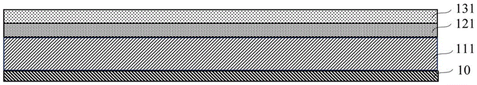
参照图1,形成晶圆的外延结构,所述晶圆的外延结构从下往上依次为衬底10、集电极层111、基极初始层121及发射极初始层131。Referring to FIG. 1 , an epitaxial structure of a wafer is formed. The epitaxial structure of the wafer includes a
其中,集电极层111可以是掺杂浓度为1016个/cm3的N型砷化镓(GaAs),基极初始层121可以是掺杂浓度为1019个/cm3的P型GaAs,发射极初始层131可以是掺杂浓度为1017个/cm3的P型GaAs。The
参照图2,在发射极初始层131上形成发射极欧姆接触电极层132。Referring to FIG. 2 , an emitter ohmic
具体可以先在发射极初始层131上涂敷一层光刻胶,再经过烘烤、曝光、显影后,通过蒸镀的方式在发射极初始层131上形成发射极欧姆接触电极层132。发射极欧姆接触电极层132可以具有依次层叠的钛(Ti)膜、铂(Pt)膜、Ti膜、Pt膜、Ti膜的多层金属层。Specifically, a layer of photoresist may be firstly coated on the emitter
参照图3,对发射极初始层131进行刻蚀,形成发射极层133。然后,在基极初始层121上形成基极欧姆接触电极层122。Referring to FIG. 3 , the emitter
比如,可以采用光刻工艺,对发射极初始层131进行刻蚀。基极欧姆接触电极层122可以具有依次层叠Pt膜、Ti膜、Pt膜、铜(Au)膜的多层金属层。For example, a photolithography process may be used to etch the emitter
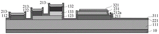
参照图4,对基极初始层121进行刻蚀,形成基极层123。然后,参照图5,在集电极初始层111上形成集电极欧姆接触电极层112及第一底层金属层211。其中,集电极欧姆接触电极层112及第一底层金属层211可以通过一次工艺形成,当然也可以通过不同的工艺先后形成。Referring to FIG. 4 , the base
比如,可以采用光刻工艺,基极初始层121进行刻蚀,然后通过蒸镀的方式,形成集电极欧姆接触电极层112及第一底层金属层211。集电极欧姆接触电极层112及第一底层金属层211的材料可以为Au。For example, a photolithography process may be used to etch the base
集电极层111及集电极欧姆接触电极层112,构成HBT的集电极结构。基极层123及基极欧姆接触电极层122,构成HBT的基极结构。发射极层133及发射极欧姆接触电极层132构成HBT的发射极结构。第一底层金属层211作为电容的下极板。The
参照图5,形成第一介质层221,所述第一介质层221同时覆盖HBT的基极结构、发射极结构及集电极结构,作为HBT的钝化层,防止HBT的基极结构、发射极结构及集电极结构侧壁被氧化。Referring to FIG. 5 , a first
其中,可以通过化学气相沉积法沉积第一介质层221。第一介质层221应当在需要导通的区域开孔。The
参照图6,形成第一顶层金属层231,所述第一顶层金属层231同时覆盖HBT的基极结构、发射极结构及集电极结构,作为HBT的钝化层,防止HBT的基极结构、发射极结构及集电极结构侧壁被氧化。在第一区域上,第一顶层金属层231还同时作为电容结构的上极板。6, a first
其中,可以通过曝光、蒸镀、金属剥离、光刻胶剥离工艺流程,形成第一顶层金属层231。所述第一顶层金属层231位于第一底层金属层211上,且与第一底层金属层211之间由第一介质层221间隔。Wherein, the first
在上述半导体结构中,电容结构通常包括:第一顶层金属层231、第一底层金属层211,以及第一顶层金属层231和第一底层金属层211之间的第一介质层221。In the above semiconductor structure, the capacitor structure generally includes: a first
实际应用中,可以通过以下三种方式来增大电容结构的容量:1)改变第一介质层221的介电常数;2)改变第一介质层221的厚度;3)增大电容结构中上极板和下极板的面积,也就是增大第一顶层金属层231和第一底层金属层211的面积。In practical applications, the capacity of the capacitor structure can be increased in the following three ways: 1) changing the dielectric constant of the
其中,第一介质层221的介电常数一般是固定的,一般为6.2左右,故很难通过改变介质层的介电常数,来增大电容结构的容量。而第一介质层221的厚度现在已经在50 nm-60nm之间,再降低的话就会有漏电的风险。The dielectric constant of the
因此,目前大都通过增大电容结构中上极板和下极板的面积这种方式,也就是增大第一顶层金属层231和第一底层金属层211的面积,来增大电容结构的容量。但是这种方式会导致整个器件面积增大,不利于器件的小型化。Therefore, at present, the capacity of the capacitor structure is mostly increased by increasing the area of the upper plate and the lower plate in the capacitor structure, that is, increasing the area of the first
针对上述问题,本发明实施例提供了一种半导体结构,所述半导体结构中,具有两个以上的电容结构,所述两个以上的电容结构之间并联连接,且在所述衬底的第一区域上沿垂直于所述衬底的方向依次层叠设置。由于两个以上的电容结构沿垂直于衬底的方向依次层叠设置,故没有额外增加电容结构占用的衬底面积,并且,两个以上的电容结构之间并联连接,故使得半导体结构的电容量增加,从而实现在不增加器件面积的情况下,增大半导体结构中电容结构的容量。另外,在本发明的实施例中,至少一个电容结构的顶部边缘区域设置有保护层,所述保护层用于覆盖所述电容结构的边缘区域,提高电容结构的可靠性。In view of the above problems, embodiments of the present invention provide a semiconductor structure, wherein the semiconductor structure has more than two capacitor structures, the two or more capacitor structures are connected in parallel, and the second capacitor structure is located on the substrate. In a region, the substrates are sequentially stacked in a direction perpendicular to the substrate. Since the two or more capacitor structures are sequentially stacked along the direction perpendicular to the substrate, the substrate area occupied by the capacitor structures is not additionally increased, and the two or more capacitor structures are connected in parallel, so that the capacitance of the semiconductor structure is increased. increase, so as to increase the capacity of the capacitor structure in the semiconductor structure without increasing the device area. In addition, in the embodiment of the present invention, a protective layer is provided on the top edge region of at least one capacitor structure, and the protective layer is used to cover the edge region of the capacitor structure to improve the reliability of the capacitor structure.
为使本发明的上述目的、特征和优点能够更为明显易懂,下面结合附图对本发明的具体实施例作详细地说明。In order to make the above objects, features and advantages of the present invention more clearly understood, the specific embodiments of the present invention will be described in detail below with reference to the accompanying drawings.
参照图7,本发明实施例提供了一种半导体结构的形成方法,所述方法可以包括如下步骤:Referring to FIG. 7 , an embodiment of the present invention provides a method for forming a semiconductor structure, and the method may include the following steps:
步骤71,提供衬底,所述衬底包括第一区域。
步骤72,在所述衬底的第一区域上形成两个以上的电容结构,所述两个以上的电容结构之间并联连接,且在所述衬底的第一区域上沿垂直于所述衬底的方向依次层叠设置。
其中,至少一个电容结构的顶部边缘区域形成有保护层,所述保护层用于覆盖所述电容结构的边缘区域,减少上方金属层的电流流至所述电容结构的边缘区域。Wherein, a protective layer is formed on the top edge region of at least one capacitor structure, and the protective layer is used to cover the edge region of the capacitor structure and reduce the current of the upper metal layer flowing to the edge region of the capacitor structure.
由于多个电容之间并联连接,故可以增大半导体结构中电容的容量。另外,多个电容结构沿垂直于衬底的方向依次层叠设置,故相对于图6,多个电容结构占用同一衬底面积,故可以不增大半导体结构的面积,更利于器件的小型化。Since a plurality of capacitors are connected in parallel, the capacity of the capacitors in the semiconductor structure can be increased. In addition, a plurality of capacitor structures are sequentially stacked along the direction perpendicular to the substrate, so compared to FIG. 6 , the multiple capacitor structures occupy the same substrate area, so the area of the semiconductor structure can not be increased, which is more conducive to the miniaturization of the device.
在具体实施中,所述衬底还可以包括第二区域,所述方法还可以包括:在所述衬底的第二区域上形成晶体管结构。其中,所述晶体管结构可以为HBT,也可以为互补金属氧化物半导体(Complementary Metal Oxide Semiconductor,CMOS)晶体管,并不作限制。In a specific implementation, the substrate may further include a second region, and the method may further include: forming a transistor structure on the second region of the substrate. Wherein, the transistor structure may be an HBT or a complementary metal oxide semiconductor (Complementary Metal Oxide Semiconductor, CMOS) transistor, which is not limited.
在具体实施中,也可以在衬底的第二区域上形成其它器件结构,只要该器件结构能够与电容结构集成在同一衬底上即可。In a specific implementation, other device structures may also be formed on the second region of the substrate, as long as the device structures and the capacitor structure can be integrated on the same substrate.
以在衬底的第二区域上形成晶体管结构,且晶体管结构为HBT为例,在所述衬底的第二区域上形成晶体管结构,可以包括:在所述衬底的第二区域上形成发射极结构、基极结构及集电极结构。Taking forming a transistor structure on the second region of the substrate and the transistor structure is HBT as an example, forming the transistor structure on the second region of the substrate may include: forming an emitter on the second region of the substrate pole structure, base structure and collector structure.
具体在衬底上形成HBT的工艺过程,可以参照上述关于图1至图6的描述进行实施,此处不再赘述。The specific process of forming the HBT on the substrate can be implemented with reference to the above descriptions with respect to FIG. 1 to FIG. 6 , and details are not repeated here.
在具体实施中,衬底的第一区域上可以仅形成两个并联连接的电容结构,也可以形成三个或三个以上并联连接的电容结构,具体电容结构的数量不作限制。In a specific implementation, only two capacitor structures connected in parallel may be formed on the first region of the substrate, or three or more capacitor structures connected in parallel may be formed, and the number of specific capacitor structures is not limited.
在一实施例中,可以仅在衬底的第一区域上形成两个并联连接的电容结构,分别为第一电容结构及第二电容结构。第一电容结构及第二电容结构之间可以共用同一金属层,也可以不共用同一金属层,即分别具有各自的金属层。In one embodiment, two capacitor structures connected in parallel may be formed only on the first region of the substrate, which are the first capacitor structure and the second capacitor structure, respectively. The first capacitor structure and the second capacitor structure may share the same metal layer, or may not share the same metal layer, that is, they each have their own metal layers.
在本发明的一实施例中,当第一顶层金属层的厚度大于150 nm时(通常为1000nm),表明第一顶层金属层厚度较厚,能够承受较大的电流,故此时,可以设置第一电容结构及第二电容结构共用所述第一顶层金属层。相应地,在所述衬底的第一区域上形成两个以上的电容结构的步骤,可以包括:In an embodiment of the present invention, when the thickness of the first top metal layer is greater than 150 nm (usually 1000 nm), it indicates that the thickness of the first top metal layer is thick and can withstand a large current. Therefore, at this time, the first top metal layer can be set to A capacitor structure and a second capacitor structure share the first top metal layer. Correspondingly, the step of forming two or more capacitor structures on the first region of the substrate may include:
在所述衬底的第一区域上,依次形成层叠设置的第一底层金属层、第一介质层及第一顶层金属层,所述第一底层金属层、第一介质层及第一顶层金属层构成第一电容结构;On the first area of the substrate, a first bottom metal layer, a first dielectric layer and a first top metal layer are sequentially formed, the first bottom metal layer, the first dielectric layer and the first top metal layer The layer constitutes a first capacitance structure;
在所述第一顶层金属层上依次形成层叠设置的第二介质层及第二顶层金属层;所述第一顶层金属层、第二介质层及第二顶层金属层,构成所述电容结构;A stacked second dielectric layer and a second top metal layer are sequentially formed on the first top metal layer; the first top metal layer, the second dielectric layer and the second top metal layer constitute the capacitor structure;
形成第一连接层,使得所述第一电容结构及第二电容结构并联连接。A first connection layer is formed so that the first capacitor structure and the second capacitor structure are connected in parallel.
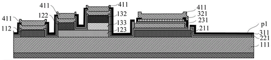
以在衬底第二区域上形成HBT为例,将图6中衬底第一区域上形成的电容结构,作为第一电容结构,参照图6,在形成第一电容结构时,在所述衬底的第一区域上,依次形成层叠设置的第一底层金属层211、第一介质层221及第一顶层金属层231。第一介质层221覆盖第一底层金属层211的上表面,第一顶层金属层231位于第一底层金属层211上方,且覆盖第一介质层221的部分表面。Taking the formation of the HBT on the second region of the substrate as an example, the capacitor structure formed on the first region of the substrate in FIG. 6 is used as the first capacitor structure, referring to FIG. On the first region of the bottom, a first
在形成第二电容结构时,参照图8,可以先在第一顶层金属层231上形成第二介质层311。参照图9,形成第二介质层311后,可以在第一顶层金属层231上方,形成覆盖第二介质层311部分表面的第二顶层金属层321。所述第一顶层金属层231、第二介质层311及第二顶层金属层321,构成所述第二电容结构。When forming the second capacitor structure, referring to FIG. 8 , a
由于第一电容结构及第二电容结构之间可以共用同一金属层,由此可以在保证电容结构可靠性的同时,简化工艺。Since the same metal layer can be shared between the first capacitor structure and the second capacitor structure, the process can be simplified while ensuring the reliability of the capacitor structure.
在图8及图9所示的实施例中,所述第一底层金属层211的厚度范围为150 nm至2000nm。In the embodiments shown in FIGS. 8 and 9 , the thickness of the first
在本发明的另一实施例中,当第一顶层金属层的厚度小于或等于150 nm时,表明第一顶层金属层厚度较薄,能够承受的电流有限,故此时,可以设置第一电容结构及第二电容结构不共用所述第一顶层金属层。在所述衬底的第一区域上形成两个以上的电容结构的步骤,可以包括:In another embodiment of the present invention, when the thickness of the first top metal layer is less than or equal to 150 nm, it indicates that the thickness of the first top metal layer is relatively thin and the current that can withstand is limited, so at this time, the first capacitor structure can be set and the second capacitor structure do not share the first top metal layer. The step of forming two or more capacitor structures on the first region of the substrate may include:
在所述衬底的第一区域上,依次形成层叠设置的第一底层金属层、第一介质层及第一顶层金属层,所述第一底层金属层、第一介质层及第一顶层金属层构成第一电容结构;On the first area of the substrate, a first bottom metal layer, a first dielectric layer and a first top metal layer are sequentially formed, the first bottom metal layer, the first dielectric layer and the first top metal layer The layer constitutes a first capacitance structure;
在所述第一顶层金属层上依次形成层叠设置的第二底层金属层、第二介质层及第二顶层金属层,所述第二底层金属层、第二介质层及第二顶层金属层构成第二电容结构;A second bottom metal layer, a second dielectric layer and a second top metal layer are sequentially formed on the first top metal layer, and the second bottom metal layer, the second dielectric layer and the second top metal layer are composed of the second capacitor structure;
形成第一连接层,使得所述第一电容结构及第二电容结构并联连接。A first connection layer is formed so that the first capacitor structure and the second capacitor structure are connected in parallel.
第一电容结构及第二电容结构之间可以不共用同一金属层,即第一电容结构及第二电容结构分别有各自独立的金属层,由此可以保证电容结构的可靠性。The first capacitor structure and the second capacitor structure may not share the same metal layer, that is, the first capacitor structure and the second capacitor structure have their own independent metal layers, thereby ensuring the reliability of the capacitor structure.
在具体实施中,可以采用化学气相沉积方法,形成第二介质层。所述第二介质层的材料也可以为氮化硅。参照图8,在形成第二介质层311时,第二介质层311也可以覆盖HBT发射极结构、集电极结构及基极结构的侧壁,由此可以作为HBT的钝化层,防止HBT中各结构被氧化。In a specific implementation, a chemical vapor deposition method can be used to form the second dielectric layer. The material of the second dielectric layer may also be silicon nitride. Referring to FIG. 8 , when the
在具体实施中,可以先在第二介质层上形成光刻胶层通过蒸镀的方式蒸镀一层金属,再对所蒸镀的执行金属玻璃通过蒸镀、金属剥离、光刻胶剥离等工艺步骤,在第二介质层上形成第二顶层金属层。所述第二顶层金属层的材料可以与第一底层金属层及第一顶层金属层的材料相同。In a specific implementation, a photoresist layer can be formed on the second dielectric layer firstly by evaporating a layer of metal, and then the evaporated metal glass can be evaporated, metal stripping, photoresist stripping, etc. In the process step, a second top metal layer is formed on the second dielectric layer. The material of the second top metal layer may be the same as that of the first bottom metal layer and the first top metal layer.
在具体实施中,参照图9,在形成第二顶层金属层321时,第二顶层金属层321也可以覆盖HBT发射极结构、集电极结构及基极结构,由此可以增加HBT的发射极结构、集电极结构及基极结构上金属层的厚度,提高晶体管的可靠性。In a specific implementation, referring to FIG. 9 , when the second
在一些实施例中,第二介质层及第二顶层金属层也可以进行形成在衬底的第一区域上。In some embodiments, the second dielectric layer and the second top metal layer may also be formed on the first region of the substrate.
在具体实施中,第一连接层可以采用多种方式,将使得所述第一电容结构及第二电容结构并联连接,此处不作限制。In a specific implementation, the first connection layer may adopt various ways to connect the first capacitor structure and the second capacitor structure in parallel, which is not limited here.
在本发明的一实施例中,参照图9,可以在第一介质层221上形成第一通孔212a,进而在第一通孔212a的位置形成所述第一连接层,使得所述第一底层金属层211与所述第二顶层金属层321连接。其中,第一介质层221上形成第一通孔212a的步骤可以包括:形成第一初始介质层;在所述第一初始介质层上形成第一通孔212a,所述第一通孔暴露出所述第一底层金属层211的表面。此时,第一连接层的一端可以与第二顶层金属层321的侧壁连接,另一端与第一底层金属层211的表面连接。此时,第二顶层金属层321的侧壁为第一连接层所覆盖。In an embodiment of the present invention, referring to FIG. 9 , a first through
在具体实施中,电流由第二顶层金属层321向下依次流经第一顶层金属层231及第一底层金属层211。为了避免电流流过金属层的边缘,在一实施例中,沿垂直于衬底的方向上,可以设置第一电容结构及第二电容结构中各金属层的有效面积逐渐缩小。其中,所谓金属层的有效面积,指的是当前金属层中能够将电流传输至下一层金属层的面积,也就是当前金属层与下一层金属层重叠的面积。In a specific implementation, the current flows downward from the second
具体地,参照图8,第一底层金属层211的有效面积大于第一顶层金属层231的有效面积,第一顶层金属层231的有效面积大于第二顶层金属层321的有效面积,由此可以尽量减少电流流过金属层的边缘而导致的放电现象,进一步提高电容结构的可靠性。Specifically, referring to FIG. 8 , the effective area of the first
在本发明的又一实施例中,所述衬底的第一区域上可以形成三个并联连接的电容结构,即在已经形成第一电容结构及第二电容结构的基础上,在第二电容结构上再形成第三电容结构。具体地,所述方法还可以包括:In yet another embodiment of the present invention, three capacitor structures connected in parallel may be formed on the first region of the substrate, that is, on the basis that the first capacitor structure and the second capacitor structure have been formed, the second capacitor A third capacitor structure is formed on the structure. Specifically, the method may also include:
在所述第二顶层金属层上依次形成层叠设置的第三底层金属层、第三介质层及第三顶层金属层,所述第三底层金属层、第三介质层及第三顶层金属层构成第三电容结构;A third bottom metal layer, a third dielectric layer and a third top metal layer are sequentially formed on the second top metal layer, and the third bottom metal layer, the third dielectric layer and the third top metal layer are composed of the third capacitor structure;
形成第二连接层,所述第二连接层连接所述第一顶层金属层及第三顶层金属层。A second connection layer is formed, and the second connection layer connects the first top metal layer and the third top metal layer.
需要说明的是,无论第一电容结构和第二电容结构,是否共用同一金属层,在具体实施中,均可以采用上述步骤形成第三电容结构。与第一电容结构及第二电容结构类似,所述第三电容结构中各金属层的有效面积沿垂直于衬底的方向自下至上逐渐减小。It should be noted that, regardless of whether the first capacitor structure and the second capacitor structure share the same metal layer, in a specific implementation, the above steps can be used to form the third capacitor structure. Similar to the first capacitor structure and the second capacitor structure, the effective area of each metal layer in the third capacitor structure gradually decreases from bottom to top along a direction perpendicular to the substrate.
在本发明的实施例中,至少一个电容结构的顶部边缘区域设置有保护层,所述保护层用于覆盖所在电容结构的边缘区域,减少上方金属层的电流流至所述电容结构的边缘区域,防止所在电容结构的周边发生放电现象,从而提高电容结构的可靠性。In an embodiment of the present invention, a protective layer is provided on the top edge region of at least one capacitor structure, and the protective layer is used to cover the edge region of the capacitor structure, so as to reduce the current flow of the upper metal layer to the edge region of the capacitor structure. , to prevent the discharge phenomenon around the capacitor structure, thereby improving the reliability of the capacitor structure.
在本发明的一实施例中,第二顶层金属层通常较薄,厚度范围为100 nm 至500nm,故所能承受的电流较小。因此,为了进一步减少电流流过第二顶层金属层的边缘而导致的放电现象,提高电容结构的可靠性,在形成第三底层金属层之前,可以形成第一保护层。所述第一保护层覆盖所述第二顶层金属层的边缘区域,并暴露所述第二通孔。In an embodiment of the present invention, the second top metal layer is generally thin, with a thickness ranging from 100 nm to 500 nm, so the current that can be endured is relatively small. Therefore, in order to further reduce the discharge phenomenon caused by the current flowing through the edge of the second top metal layer and improve the reliability of the capacitor structure, before forming the third bottom metal layer, a first protective layer may be formed. The first protective layer covers an edge region of the second top metal layer and exposes the second through hole.
具体地,以在图9的基础上形成第三电容结构为例,参照图10,形成第二顶层金属层321后,可以先形成第一保护层p1,所述第一保护层p1可以覆盖第二顶层金属层321的边缘区域,覆盖第二电容结构的周边,由此后续在第一保护层p1上形成第三底层金属层411时,可以进一步减小第三底层金属层411与第二顶层金属层321的接触面积,从而可以进一步避免第三底层金属层411的电流流至第二顶层金属层321的边缘区域,进一步提高电容结构的可靠性。Specifically, taking the formation of the third capacitor structure on the basis of FIG. 9 as an example, referring to FIG. 10 , after the second
在一些实施例中,第一保护层也可以仅形成在衬底的第一区域上,而不形成在HBT上。In some embodiments, the first protective layer may also be formed only on the first region of the substrate and not on the HBT.
在具体实施中,所述第一保护层p1的材料可以为聚合物,比如聚酰亚胺(Polyimide)。所述第一保护层p1具有绝缘、耐高温、防水以及防氧化的特性,故可以避免第三底层金属层411的电流流至第二顶层金属层321的边缘区域。其中,所述第一保护层p1的厚度可以根据器件实际应用、器件高低差以及可靠性要求等因素进行设置,具体厚度范围可以为500 nm至5000 nm。In a specific implementation, the material of the first protective layer p1 may be a polymer, such as polyimide (Polyimide). The first protective layer p1 has the properties of insulation, high temperature resistance, water resistance and oxidation resistance, so that the current of the third
在具体实施中,所述第一保护层p1还可以同时覆盖第二介质层311,以及HBT中发射极结构、集电极结构、基极结构的边缘区域,由此可以对相应器件进行保护。In a specific implementation, the first protective layer p1 may also cover the
在具体实施中,可以平坦化涂布的方式形成所述第一保护层p1,当然,也可以采用其它工艺形成所述第一保护层p1,此处不作限制。In a specific implementation, the first protective layer p1 may be formed by planarizing coating. Of course, other processes may also be used to form the first protective layer p1, which is not limited here.
参照图11,形成第一保护层p1后,可以在第一保护层p1及第二顶层金属层321上形成第三底层金属层411。Referring to FIG. 11 , after the first protective layer p1 is formed, a third
参照图12,形成第三底层金属层411后,再形成第三底层金属层411上形成第三介质层421。Referring to FIG. 12 , after the third
参照图13,形成第三介质层421,在第三介质层421上形成第三顶层金属层431。Referring to FIG. 13 , a third
在具体实施中,可以通过蒸镀、金属剥离、光刻胶剥离的工艺步骤,在第一保护层p1上形成第三底层金属层411,以及在第三介质层421上形成第三顶层金属层431。所述第三底层金属层411的材料及第三顶层金属层431,可以与第二电容结构及第一电容结构中金属层的材料相同。In a specific implementation, a third
在具体实施中,所述第三底层金属层411的厚度范围为1000 nm至8000 nm,所述第三顶层金属层431的厚度范围为100 nm至500 nm。In a specific implementation, the thickness of the third
在一实施例中,在第二顶层金属层321上形成第三底层金属层411时,可以同时覆盖HBT的发射极结构、集电极结构及基极结构形成第三底层金属层411,以进一步增加HBT的发射极结构、集电极结构及基极结构上金属层的厚度,提高晶体管的可靠性。In one embodiment, when the third
在一些实施例中,第三底层金属层也可以进行形成在衬底的第一区域上。In some embodiments, a third underlying metal layer may also be formed on the first region of the substrate.
在具体实施中,参照图13,可以通过化学气相沉积法形成所述第三介质层421。所述第一介质层221、所述第二介质层321及第三介质层421的厚度范围可以根据器件要求、工艺能力以及器件可靠性要求等因素进行设置。在本发明的实施例中,所述第一介质层221、所述第二介质层321及第三介质层421的厚度范围可以相同,比如60 nm或者160 nm,均可以在40 nm至500 nm范围内。In a specific implementation, referring to FIG. 13 , the third
在具体实施中,所述第一介质层221、所述第二介质层321及第三介质层421的材料可以相同,均可以为氮化硅,当然也可以为其它材料。In a specific implementation, the materials of the
在本发明的一实施例中,可以在形成第三顶层金属层后,形成第一连接层及第二连接层。其中,所述第一连接层用于连接第一电容结构及第二电容结构,第二连接层用于连接第一电容结构和第三电容结构。In an embodiment of the present invention, the first connection layer and the second connection layer may be formed after the third top metal layer is formed. Wherein, the first connection layer is used to connect the first capacitor structure and the second capacitor structure, and the second connection layer is used to connect the first capacitor structure and the third capacitor structure.
在具体实施中,第一连接层可以通过将第一底层金属层与第二顶层金属层直接连接的方式,连接第一电容结构及第二电容结构。在第二顶层金属层上设置有第一保护层时,由于第一保护层覆盖第二顶层金属层及第二介质层,此时,第一连接层也可以通过将第三底层金属层与第一底层金属层相连接的方式,或者通过将第一顶层金属层与第三底层金属层直接连接的方式,使得第一底层金属层与第二顶层金属层间接连接,同样也可以连接第一电容结构及第二电容结构。In a specific implementation, the first connection layer can connect the first capacitor structure and the second capacitor structure by directly connecting the first bottom metal layer and the second top metal layer. When the first protective layer is provided on the second top metal layer, since the first protective layer covers the second top metal layer and the second dielectric layer, at this time, the first connection layer can also connect the third bottom metal layer with the second dielectric layer. A bottom metal layer is connected, or by directly connecting the first top metal layer and the third bottom metal layer, so that the first bottom metal layer and the second top metal layer are indirectly connected, and the first capacitor can also be connected. structure and a second capacitor structure.
例如,参照图15,第一连接层L1的一端经第一介质层221上的第一通孔212a(如图9所示)与第一底层金属层211连接,另一端经第三底层金属层411与第二顶层金属层321连接。For example, referring to FIG. 15 , one end of the first connection layer L1 is connected to the first
在具体实施中,当第一连接层连接第一底层金属层与第二顶层金属层时,或者第一连接层连接第三底层金属层与第一底层金属层时,所述第二连接层可以通过将第一顶层金属层与第三顶层金属层直接连接的方式,连接第一电容结构和第三电容结构。当第一连接层连接第一顶层金属层与第三底层金属层时,所述第二连接层可以通过连接第一底层金属层及第三顶层金属层的方式,连接第一电容结构和第三电容结构。In a specific implementation, when the first connecting layer connects the first bottom metal layer and the second top metal layer, or when the first connecting layer connects the third bottom metal layer and the first bottom metal layer, the second connecting layer may The first capacitor structure and the third capacitor structure are connected by directly connecting the first top metal layer and the third top metal layer. When the first connecting layer connects the first top metal layer and the third bottom metal layer, the second connecting layer can connect the first capacitor structure and the third capacitor structure by connecting the first bottom metal layer and the third top metal layer Capacitive structure.
例如,参照图14,形成所述第二介质层311的步骤可以包括:先形成第二初始介质层,再在所述第二初始介质层上形成第二通孔311a,所述第二通孔311a暴露出所述第一顶层金属层231的表面。参照图15,形成所述第二连接层的步骤包括:在所述第二通孔311a(如图14所示)的位置形成所述第二连接层L2,使得所述第一顶层金属层231与所述第三顶层金属层431连接。For example, referring to FIG. 14 , the step of forming the
需要说明的是,在具体实施中,参照图15,当第一介质层221上形成有第一通孔时,除第一连接层L1外,第一介质层221上的各层,在形成时,均暴露该第一通孔。同样地,在第二介质层311上行有第二通孔时,第二介质层311上的各层,除第二连接层L2外,在形成时,均暴露该第二通孔。It should be noted that, in a specific implementation, referring to FIG. 15 , when a first through hole is formed on the
在具体实施中,参照图15,所述第一连接层L1及第二连接层L2可以同时形成。比如,可以通过蒸镀、金属剥离、光刻胶剥离等工艺流程,同时形成第一连接层L1及第二连接层L2。第一连接层L1及第二连接层L2的材料可以为Au。In a specific implementation, referring to FIG. 15 , the first connection layer L1 and the second connection layer L2 may be formed at the same time. For example, the first connection layer L1 and the second connection layer L2 may be formed simultaneously through the process flow of evaporation, metal stripping, photoresist stripping, and the like. The material of the first connection layer L1 and the second connection layer L2 may be Au.
在具体实施中,参照图15,在形成第一连接层L1及第二连接层L2的同时,也可以在HBT的发射极结构、集电极结构及基极结构上形成第二连接层L2(或第一连接层L1),以进一步增加HBT的发射极结构、集电极结构及基极结构上金属层的厚度,提高晶体管的可靠性。In a specific implementation, referring to FIG. 15 , while the first connection layer L1 and the second connection layer L2 are formed, the second connection layer L2 (or the second connection layer L2 (or the HBT) can also be formed on the emitter structure, collector structure and base structure of the HBT. The first connection layer L1), to further increase the thickness of the metal layer on the emitter structure, collector structure and base structure of the HBT, and improve the reliability of the transistor.
在一些实施例中,第一连接层及第二连接层也可以仅形成在衬底的第一区域上,而不形成在HBT上。In some embodiments, the first connection layer and the second connection layer may also be formed only on the first region of the substrate, but not on the HBT.
在本发明的一实施例中,参照图14及图15,在形成所述第三顶层金属层431之后,形成第二连接层L2之前,形成第二保护层p2;所述第二保护层p2可以覆盖所述第三顶层金属层431的边缘区域,并暴露所述第二通孔311a;所述第二保护层p2具有暴露所述第三顶层金属层431表面的第三通孔p21。In an embodiment of the present invention, referring to FIGS. 14 and 15 , after the third
此时,所述第二保护层p2可以覆盖第三顶层金属层431的边缘区域,进而覆盖第三电容结构的周边,避免后续流入第三顶层金属层431的电流流至第三顶层金属层431的边缘区域,导致第三顶层金属层431发生放电现象,进一步提高电容的可靠性。所述第二保护层p2也可以覆盖HBT的发射极结构、集电极结构及基极结构的边缘区域,防止HBT发生漏电,提高HBT的可靠性。另外,第二保护层p2还可以覆盖第三顶层金属层431的大部分区域,还可以覆盖HBT的发射极结构、集电极结构及基极结构的侧壁,作为钝化层,防止第三顶层金属层431被氧化。At this time, the second protection layer p2 can cover the edge region of the third
在一些实施例中,第二保护层也可以仅形成在衬底的第一区域上,而不形成在HBT上。In some embodiments, the second protective layer may also be formed only on the first region of the substrate and not on the HBT.
在具体实施中,所述第二保护层p2的材料与第一保护层p1的材料可以相同,均可以为聚酰亚胺(Polyimide)。所述第二保护层p2的厚度范围为500 nm至5000 nm,具体根据实际应用、器件高低差以及可靠性要求等因素进行调整即可。In a specific implementation, the material of the second protective layer p2 and the material of the first protective layer p1 may be the same, and both may be polyimide. The thickness of the second protective layer p2 is in the range of 500 nm to 5000 nm, which may be adjusted according to factors such as actual applications, device height differences, and reliability requirements.
参照图14及图15,形成第二保护层p2后,形成所述第二连接层L2的步骤可以包括:在所述第二通孔311a及所述第三通孔p21的位置形成所述第二连接层L2,所述第二连接层L2连接所述第三顶层金属层431及所述第一顶层金属层231。14 and 15 , after the second protective layer p2 is formed, the step of forming the second connection layer L2 may include: forming the first through
需要说明的是,衬底第二区域上形成的器件,并不限于HBT,还可以为其它器件,HBT仅是在衬底第二区域上所形成器件的一个示例而已。It should be noted that the device formed on the second region of the substrate is not limited to the HBT, but may also be other devices, and the HBT is only an example of the device formed on the second region of the substrate.
由上述内容可知,本发明实施例中半导体结构的形成方法,由于在衬底的同一位置上形成两个以上并联的电容结构,由此可以增大半导体结构中电容的容量,并且未额外增加占用的衬底面积,实现了在不增加器件面积的情况下,增大半导体结构中电容结构的容量的目的。It can be seen from the above content that, in the method for forming the semiconductor structure in the embodiment of the present invention, since two or more parallel capacitor structures are formed on the same position of the substrate, the capacity of the capacitor in the semiconductor structure can be increased without additional occupation. The purpose of increasing the capacity of the capacitor structure in the semiconductor structure is achieved without increasing the area of the device.
另外,本发明的实施例中,由于第一保护层的设置,可以覆盖第二电容结构的周边,减小第三底层金属层与第二顶层金属层的接触面积,避免第三底层金属层的电流流至第二顶层金属层的边缘区域,提高电容的可靠性。In addition, in the embodiment of the present invention, due to the arrangement of the first protective layer, the periphery of the second capacitor structure can be covered, the contact area between the third bottom metal layer and the second top metal layer is reduced, and the third bottom metal layer can be avoided. The current flows to the edge region of the second top metal layer, improving the reliability of the capacitor.
再者,本发明的实施例中,由于第二保护层的设置,可以覆盖第三电容结构的周边,避免外部电流流至第三顶层金属层的边缘区域,进一步提高电容的可靠性。Furthermore, in the embodiment of the present invention, due to the disposition of the second protective layer, the periphery of the third capacitor structure can be covered to prevent external current from flowing to the edge region of the third top metal layer, thereby further improving the reliability of the capacitor.
为了使本领域技术人员更好地理解和实现本发明,以下对上述方法对应的半导体结构进行详细描述。In order to make those skilled in the art better understand and implement the present invention, the semiconductor structure corresponding to the above method is described in detail below.
本发明实施例提供了一种半导体结构,所述半导体结构可以包括:Embodiments of the present invention provide a semiconductor structure, and the semiconductor structure may include:
衬底,所述衬底包括第一区域;a substrate including a first region;
两个以上的电容结构,所述两个以上的电容结构之间并联连接,且在所述衬底的第一区域上沿垂直于所述衬底的方向依次层叠设置。Two or more capacitor structures are connected in parallel, and are sequentially stacked on the first region of the substrate along a direction perpendicular to the substrate.
在本发明的一实施例中,衬底还可以包括第二区域,所述第二区域上可以形成晶体管结构。In an embodiment of the present invention, the substrate may further include a second region on which a transistor structure may be formed.
在本发明的一实施例中,参照图15,所述晶体管结构可以为HBT,所述HBT包括:位于所述衬底第二区域上的发射极结构、基极结构及集电极结构。In an embodiment of the present invention, referring to FIG. 15 , the transistor structure may be an HBT, and the HBT includes an emitter structure, a base structure and a collector structure on the second region of the substrate.
在具体实施中,衬底的第一区域上可以仅形成两个并联连接的电容结构,也可以形成三个或三个以上并联连接的电容结构,具体电容结构的数量不作限制。In a specific implementation, only two capacitor structures connected in parallel may be formed on the first region of the substrate, or three or more capacitor structures connected in parallel may be formed, and the number of specific capacitor structures is not limited.
在本发明的一实施例中,参照图15,衬底的第一区域上可以形成三个并联连接的电容结构,分别为第一电容结构、第二电容结构及第三电容结构。其中:In an embodiment of the present invention, referring to FIG. 15 , three capacitor structures connected in parallel may be formed on the first region of the substrate, namely a first capacitor structure, a second capacitor structure and a third capacitor structure. in:
所述第一电容结构可以包括:依次层叠设置的第一底层金属层211、第一介质层221及第一顶层金属层231;The first capacitor structure may include: a first
所述第二电容结构可以包括:依次层叠设置的第一顶层金属层231、第二介质层311及第二顶层金属层321;The second capacitor structure may include: a first
所述第一连接层L1连接所述第一顶层金属层231及所述第二顶层金属层321。The first connection layer L1 connects the first
在本发明的另一实施例中,所述衬底的第一区域上也可以仅形成两个并联连接的电容结构,分别为第一电容结构及第二电容结构,所述第一电容结构位于衬底第一区域上,所述第二电容结构位于所述第一电容结构上方。第一电容结构及第二电容结构之间通过第一连接层实现并联连接。In another embodiment of the present invention, only two capacitor structures connected in parallel may be formed on the first region of the substrate, which are a first capacitor structure and a second capacitor structure, and the first capacitor structure is located at On the first region of the substrate, the second capacitor structure is located above the first capacitor structure. The first capacitor structure and the second capacitor structure are connected in parallel through the first connection layer.
在一实施例中,第一电容结构及第二电容结构可以共用同一金属层。In one embodiment, the first capacitor structure and the second capacitor structure may share the same metal layer.
参照图15,具体地,依次层叠设置的第一底层金属层211、第一介质层221及第一顶层金属层231,构成所述第一电容结构;15 , specifically, the first
依次层叠设置的第一顶层金属层231、第二介质层311及第二顶层金属层321,构成第二电容结构;The first
所述第一连接层L1连接所述第一顶层金属层231及所述第二顶层金属层321。The first connection layer L1 connects the first
此时,第一电容结构及第二电容结构共用第二顶层金属层321,即第二顶层金属层321既作为第一电容结构的上极板,也同时作为第二电容结构的下极板,由此可以在保证电容结构可靠性的同时,简化减工艺。At this time, the first capacitor structure and the second capacitor structure share the second
在其它实施例中,第一电容结构及第二电容结构也可以不共用同一金属层。In other embodiments, the first capacitor structure and the second capacitor structure may not share the same metal layer.
参照图15,具体地,依次层叠设置的第一底层金属层211、第一介质层221及第一顶层金属层231,构成所述第一电容结构;15 , specifically, the first
依次层叠设置的第二底层金属层(未示出)第二介质层311及第二顶层金属层321,构成所述第二电容结构;The second bottom metal layer (not shown), the
所述第一连接层L1连接所述第一顶层金属层231及所述第二顶层金属层321。The first connection layer L1 connects the first
在具体实施中,为了将第一顶层金属层及所述第二顶层金属层321进行连接,所述第一介质层221可以具有暴露出所述第一底层金属层211表面的第一通孔212a(参照图9),所述第一连接层L1通过所述第一通孔212a与所述第一底层金属层211连接。所述第一连接层L1的另一端可以与第二顶层金属层321直接连接,也可以通过第三底层金属层421间接与第二顶层金属层321连接。In a specific implementation, in order to connect the first top metal layer and the second
在具体实施中,为了将第一顶层金属层231与第三顶层金属层431进行连接,所述第二介质层311可以具有暴露出所述第一顶层金属层231表面的第二通孔311a(如图14所示),所述第二连接层L2通过所述第二通孔311a与所述第三顶层金属层431连接。所述第二连接层L2可以直接与第三顶层金属层431连接。In a specific implementation, in order to connect the first
在本发明的一实施例中,参照图15,所述两个以上的电容结构还可以包括:第一保护层p1,覆盖所述第二顶层金属层321的边缘区域;所述第一保护层p1覆盖所述第二顶层金属层321的边缘区域,并暴露所述第二通孔311a(如图14所示)。In an embodiment of the present invention, referring to FIG. 15 , the two or more capacitor structures may further include: a first protective layer p1 covering the edge region of the second
通过设置第一保护层p1,可以将第二电容结构的周边覆盖,减少第三底层金属层411的电流流至第二顶层金属层321的边缘区域,导致第二电容结构发生漏电。By arranging the first protective layer p1, the periphery of the second capacitor structure can be covered, and the current of the third
在本发明的另一实施例中,所述两个以上的电容结构还可以包括:第二保护层p2;所述第二保护层p2覆盖所述第三顶层金属层411的边缘区域,并暴露所述第二通孔311a(如图14所示);所述第二保护层p2具有暴露所述第三顶层金属层411表面的第三通孔,所述第二连接层L2通过所述第二通孔311a及所述第三通孔,连接所述第三顶层金属层411及所述第一顶层金属层231。In another embodiment of the present invention, the two or more capacitor structures may further include: a second protective layer p2; the second protective layer p2 covers the edge region of the third
通过设置第二保护层p2,可以将第三电容结构的周边覆盖,减少外部电流流至第三顶层金属层431的边缘区域,导致第三电容结构发生漏电。By arranging the second protective layer p2, the periphery of the third capacitor structure can be covered to reduce the flow of external current to the edge region of the third
在具体实施中,在衬底第一区域上形成第一顶层金属层、第二顶层金属层、第一连接层及第二连接层时,可以在HBT的发射极结构、集电极结构及基极结构上同时形成相应的金属层,也可以仅在HBT上形成其中部分金属层,使得HBT的发射极结构、基极结构及集电极结构,均包括所述两个以上的电容结构中至少两个金属层,以增大HBT中金属层的厚度,提高HBT的可靠性。In a specific implementation, when the first top metal layer, the second top metal layer, the first connection layer and the second connection layer are formed on the first region of the substrate, the emitter structure, collector structure and base of the HBT may be formed. Corresponding metal layers are formed on the structure at the same time, or only part of the metal layers can be formed on the HBT, so that the emitter structure, base structure and collector structure of the HBT all include at least two of the two or more capacitor structures. The metal layer is used to increase the thickness of the metal layer in the HBT and improve the reliability of the HBT.
在具体实施中,形成第一保护层p1及第二保护层p2时,也可以在HBT的发射极结构、集电极结构及基极结构上同时形成,使得第一保护层p1及第二保护层p2覆盖发射极结构、集电极结构及基极结构的侧壁及边缘区域,在保护HBT的同时,提高HBT的可靠性。In a specific implementation, when the first protective layer p1 and the second protective layer p2 are formed, they can also be formed on the emitter structure, collector structure and base structure of the HBT at the same time, so that the first protective layer p1 and the second protective layer are formed at the same time. p2 covers the sidewalls and edge regions of the emitter structure, the collector structure and the base structure, so as to protect the HBT and improve the reliability of the HBT.
由上述内容可知,本发明实施例中的半导体结构,在同一衬底上集成HBT及两个以上电容结构,由于电容结构之间并联连接,故可以增大半导体结构中电容的容量,而且没有额外占用衬底面积,实现在不增加器件面积的情况下,增大半导体结构中电容结构的容量的目的。It can be seen from the above content that the semiconductor structure in the embodiment of the present invention integrates HBT and two or more capacitor structures on the same substrate. Since the capacitor structures are connected in parallel, the capacitance of the capacitor in the semiconductor structure can be increased, and there is no additional The substrate area is occupied to achieve the purpose of increasing the capacity of the capacitor structure in the semiconductor structure without increasing the device area.
虽然本发明披露如上,但本发明并非限定于此。任何本领域技术人员,在不脱离本发明的精神和范围内,均可作各种更动与修改,因此本发明的保护范围应当以权利要求所限定的范围为准。Although the present invention is disclosed above, the present invention is not limited thereto. Any person skilled in the art can make various changes and modifications without departing from the spirit and scope of the present invention. Therefore, the protection scope of the present invention should be based on the scope defined by the claims.
Claims (23)
Priority Applications (3)
| Application Number | Priority Date | Filing Date | Title |
|---|---|---|---|
| CN202210964612.7A CN115050737B (en) | 2022-08-12 | 2022-08-12 | Semiconductor structure and forming method thereof |
| PCT/CN2023/110710 WO2024032437A1 (en) | 2022-08-12 | 2023-08-02 | Semiconductor structure and method for forming same |
| EP23851658.7A EP4571836A1 (en) | 2022-08-12 | 2023-08-02 | Semiconductor structure and method for forming same |
Applications Claiming Priority (1)
| Application Number | Priority Date | Filing Date | Title |
|---|---|---|---|
| CN202210964612.7A CN115050737B (en) | 2022-08-12 | 2022-08-12 | Semiconductor structure and forming method thereof |
Publications (2)
| Publication Number | Publication Date |
|---|---|
| CN115050737A true CN115050737A (en) | 2022-09-13 |
| CN115050737B CN115050737B (en) | 2022-12-06 |
Family
ID=83167015
Family Applications (1)
| Application Number | Title | Priority Date | Filing Date |
|---|---|---|---|
| CN202210964612.7A Active CN115050737B (en) | 2022-08-12 | 2022-08-12 | Semiconductor structure and forming method thereof |
Country Status (3)
| Country | Link |
|---|---|
| EP (1) | EP4571836A1 (en) |
| CN (1) | CN115050737B (en) |
| WO (1) | WO2024032437A1 (en) |
Cited By (4)
| Publication number | Priority date | Publication date | Assignee | Title |
|---|---|---|---|---|
| CN115579299A (en) * | 2022-11-21 | 2023-01-06 | 常州承芯半导体有限公司 | Semiconductor structures and methods of forming them |
| CN115621125A (en) * | 2022-12-16 | 2023-01-17 | 常州承芯半导体有限公司 | Method for forming heterojunction bipolar transistor structure |
| CN116209353A (en) * | 2023-05-06 | 2023-06-02 | 常州承芯半导体有限公司 | Capacitor structure and forming method thereof, semiconductor structure and forming method thereof |
| WO2024032437A1 (en) * | 2022-08-12 | 2024-02-15 | 常州承芯半导体有限公司 | Semiconductor structure and method for forming same |
Citations (3)
| Publication number | Priority date | Publication date | Assignee | Title |
|---|---|---|---|---|
| JPS6074470A (en) * | 1983-09-29 | 1985-04-26 | Fujitsu Ltd | Semiconductor device |
| CN103985707A (en) * | 2014-04-24 | 2014-08-13 | 无锡市晶源微电子有限公司 | Capacitor of sandwich structure |
| CN111739895A (en) * | 2020-06-29 | 2020-10-02 | 福建华佳彩有限公司 | A TFT backplane structure and manufacturing method |
Family Cites Families (5)
| Publication number | Priority date | Publication date | Assignee | Title |
|---|---|---|---|---|
| KR100959445B1 (en) * | 2007-12-17 | 2010-05-25 | 주식회사 동부하이텍 | Capacitor of semiconductor device and manufacturing method thereof |
| KR20140083150A (en) * | 2012-12-24 | 2014-07-04 | 엘지디스플레이 주식회사 | Organic electro luminescent device and method of fabricating the same |
| CN104795428A (en) * | 2015-04-10 | 2015-07-22 | 京东方科技集团股份有限公司 | Array substrate, manufacturing method thereof and display device |
| DE102018108908B4 (en) * | 2017-11-21 | 2022-09-29 | Taiwan Semiconductor Manufacturing Co., Ltd. | Structure and formation method of a semiconductor device with capacitors |
| CN115050737B (en) * | 2022-08-12 | 2022-12-06 | 常州承芯半导体有限公司 | Semiconductor structure and forming method thereof |
-
2022
- 2022-08-12 CN CN202210964612.7A patent/CN115050737B/en active Active
-
2023
- 2023-08-02 EP EP23851658.7A patent/EP4571836A1/en active Pending
- 2023-08-02 WO PCT/CN2023/110710 patent/WO2024032437A1/en not_active Ceased
Patent Citations (3)
| Publication number | Priority date | Publication date | Assignee | Title |
|---|---|---|---|---|
| JPS6074470A (en) * | 1983-09-29 | 1985-04-26 | Fujitsu Ltd | Semiconductor device |
| CN103985707A (en) * | 2014-04-24 | 2014-08-13 | 无锡市晶源微电子有限公司 | Capacitor of sandwich structure |
| CN111739895A (en) * | 2020-06-29 | 2020-10-02 | 福建华佳彩有限公司 | A TFT backplane structure and manufacturing method |
Cited By (5)
| Publication number | Priority date | Publication date | Assignee | Title |
|---|---|---|---|---|
| WO2024032437A1 (en) * | 2022-08-12 | 2024-02-15 | 常州承芯半导体有限公司 | Semiconductor structure and method for forming same |
| CN115579299A (en) * | 2022-11-21 | 2023-01-06 | 常州承芯半导体有限公司 | Semiconductor structures and methods of forming them |
| CN115579299B (en) * | 2022-11-21 | 2023-04-14 | 常州承芯半导体有限公司 | Semiconductor structures and methods of forming them |
| CN115621125A (en) * | 2022-12-16 | 2023-01-17 | 常州承芯半导体有限公司 | Method for forming heterojunction bipolar transistor structure |
| CN116209353A (en) * | 2023-05-06 | 2023-06-02 | 常州承芯半导体有限公司 | Capacitor structure and forming method thereof, semiconductor structure and forming method thereof |
Also Published As
| Publication number | Publication date |
|---|---|
| WO2024032437A1 (en) | 2024-02-15 |
| CN115050737B (en) | 2022-12-06 |
| EP4571836A1 (en) | 2025-06-18 |
Similar Documents
| Publication | Publication Date | Title |
|---|---|---|
| CN115050737B (en) | Semiconductor structure and forming method thereof | |
| US11527512B2 (en) | Method for fabricating semiconductor device with connecting structure | |
| US11631655B2 (en) | Semiconductor device with connection structure and method for fabricating the same | |
| US9786592B2 (en) | Integrated circuit structure and method of forming the same | |
| JP2004111624A (en) | Semiconductor device | |
| US20240274554A1 (en) | Semiconductor device with composite conductive features and method for fabricating the same | |
| US10720498B2 (en) | Semiconductor device structure and method of manufacture | |
| WO2024109515A1 (en) | Semiconductor structure and forming method therefor | |
| US20260052710A1 (en) | Semiconductor structure and method for forming same | |
| US11315893B2 (en) | Semiconductor device with composite connection structure and method for fabricating the same | |
| JPS63211672A (en) | Semiconductor integrated circuit device | |
| CN110767650B (en) | SMIM capacitor structure for improving breakdown resistance and manufacturing method | |
| US10395085B2 (en) | Semiconductor device and fingerprint sensor device thereof | |
| JP2001298154A (en) | Semiconductor device and method of manufacturing the same | |
| US20250357307A1 (en) | Backside metal-insulator-metal capacitor | |
| US20220415705A1 (en) | Integrated electronic device with a pad structure including a barrier structure and related manufacturing process | |
| TW202002312A (en) | Metal-insulator-metal capacitor | |
| TWI629763B (en) | Semiconductor device and fingerprint sensor device thereof | |
| JPH0654794B2 (en) | Semiconductor integrated circuit | |
| JP3204393B2 (en) | Semiconductor device | |
| CN118647259A (en) | Capacitor structure and method for forming same, and semiconductor structure | |
| WO2025026326A1 (en) | Mim capacitor and manufacturing method therefor | |
| KR0147636B1 (en) | Semiconductor device having wiring structure to protect thin junction and manufacturing method thereof | |
| CN116209353A (en) | Capacitor structure and forming method thereof, semiconductor structure and forming method thereof | |
| CN115602664A (en) | III-V semiconductor chip |
Legal Events
| Date | Code | Title | Description |
|---|---|---|---|
| PB01 | Publication | ||
| PB01 | Publication | ||
| SE01 | Entry into force of request for substantive examination | ||
| SE01 | Entry into force of request for substantive examination | ||
| GR01 | Patent grant | ||
| GR01 | Patent grant |