CN114959565A - Vapor deposition mask, vapor deposition mask with frame, method for manufacturing organic semiconductor element, and method for manufacturing organic EL display - Google Patents
Vapor deposition mask, vapor deposition mask with frame, method for manufacturing organic semiconductor element, and method for manufacturing organic EL display Download PDFInfo
- Publication number
- CN114959565A CN114959565A CN202210442665.2A CN202210442665A CN114959565A CN 114959565 A CN114959565 A CN 114959565A CN 202210442665 A CN202210442665 A CN 202210442665A CN 114959565 A CN114959565 A CN 114959565A
- Authority
- CN
- China
- Prior art keywords
- mask
- vapor deposition
- metal mask
- metal
- resin
- Prior art date
- Legal status (The legal status is an assumption and is not a legal conclusion. Google has not performed a legal analysis and makes no representation as to the accuracy of the status listed.)
- Pending
Links
- 238000007740 vapor deposition Methods 0.000 title claims abstract description 337
- 238000000034 method Methods 0.000 title claims description 48
- 238000004519 manufacturing process Methods 0.000 title claims description 37
- 239000004065 semiconductor Substances 0.000 title claims description 29
- 229910052751 metal Inorganic materials 0.000 claims abstract description 360
- 239000002184 metal Substances 0.000 claims abstract description 360
- 229920005989 resin Polymers 0.000 claims abstract description 231
- 239000011347 resin Substances 0.000 claims abstract description 231
- 238000010030 laminating Methods 0.000 claims abstract description 5
- 239000000463 material Substances 0.000 description 21
- 230000002093 peripheral effect Effects 0.000 description 18
- 238000000151 deposition Methods 0.000 description 13
- 230000008021 deposition Effects 0.000 description 12
- 230000002787 reinforcement Effects 0.000 description 12
- 239000012044 organic layer Substances 0.000 description 8
- 239000007769 metal material Substances 0.000 description 7
- 238000006073 displacement reaction Methods 0.000 description 6
- 239000010410 layer Substances 0.000 description 6
- 239000000696 magnetic material Substances 0.000 description 6
- 230000003014 reinforcing effect Effects 0.000 description 5
- 238000010586 diagram Methods 0.000 description 4
- 238000010521 absorption reaction Methods 0.000 description 3
- 239000012790 adhesive layer Substances 0.000 description 3
- 230000015572 biosynthetic process Effects 0.000 description 3
- 230000007423 decrease Effects 0.000 description 3
- 230000000149 penetrating effect Effects 0.000 description 3
- 238000003825 pressing Methods 0.000 description 3
- 229910001030 Iron–nickel alloy Inorganic materials 0.000 description 2
- 239000000853 adhesive Substances 0.000 description 2
- 238000005229 chemical vapour deposition Methods 0.000 description 2
- 238000005520 cutting process Methods 0.000 description 2
- 230000000694 effects Effects 0.000 description 2
- 238000005530 etching Methods 0.000 description 2
- 238000005240 physical vapour deposition Methods 0.000 description 2
- 239000000758 substrate Substances 0.000 description 2
- QNRATNLHPGXHMA-XZHTYLCXSA-N (r)-(6-ethoxyquinolin-4-yl)-[(2s,4s,5r)-5-ethyl-1-azabicyclo[2.2.2]octan-2-yl]methanol;hydrochloride Chemical compound Cl.C([C@H]([C@H](C1)CC)C2)CN1[C@@H]2[C@H](O)C1=CC=NC2=CC=C(OCC)C=C21 QNRATNLHPGXHMA-XZHTYLCXSA-N 0.000 description 1
- 229910000838 Al alloy Inorganic materials 0.000 description 1
- 229920000298 Cellophane Polymers 0.000 description 1
- 229920000219 Ethylene vinyl alcohol Polymers 0.000 description 1
- 229910001374 Invar Inorganic materials 0.000 description 1
- 239000004962 Polyamide-imide Substances 0.000 description 1
- 239000004743 Polypropylene Substances 0.000 description 1
- 239000004372 Polyvinyl alcohol Substances 0.000 description 1
- 229920001328 Polyvinylidene chloride Polymers 0.000 description 1
- 238000009825 accumulation Methods 0.000 description 1
- 230000001070 adhesive effect Effects 0.000 description 1
- 239000000956 alloy Substances 0.000 description 1
- 229910010293 ceramic material Inorganic materials 0.000 description 1
- 239000003086 colorant Substances 0.000 description 1
- 230000003247 decreasing effect Effects 0.000 description 1
- 230000007547 defect Effects 0.000 description 1
- 229910003460 diamond Inorganic materials 0.000 description 1
- 239000010432 diamond Substances 0.000 description 1
- 238000005401 electroluminescence Methods 0.000 description 1
- 238000000313 electron-beam-induced deposition Methods 0.000 description 1
- 229920005648 ethylene methacrylic acid copolymer Polymers 0.000 description 1
- 239000005038 ethylene vinyl acetate Substances 0.000 description 1
- 239000011521 glass Substances 0.000 description 1
- 238000007733 ion plating Methods 0.000 description 1
- 229920000554 ionomer Polymers 0.000 description 1
- 239000003562 lightweight material Substances 0.000 description 1
- 230000003287 optical effect Effects 0.000 description 1
- 238000005268 plasma chemical vapour deposition Methods 0.000 description 1
- 238000007747 plating Methods 0.000 description 1
- 229920001200 poly(ethylene-vinyl acetate) Polymers 0.000 description 1
- 229920006350 polyacrylonitrile resin Polymers 0.000 description 1
- 229920006122 polyamide resin Polymers 0.000 description 1
- 229920002312 polyamide-imide Polymers 0.000 description 1
- 229920005668 polycarbonate resin Polymers 0.000 description 1
- 239000004431 polycarbonate resin Substances 0.000 description 1
- 229920001225 polyester resin Polymers 0.000 description 1
- 239000004645 polyester resin Substances 0.000 description 1
- 229920013716 polyethylene resin Polymers 0.000 description 1
- 229920001721 polyimide Polymers 0.000 description 1
- 239000009719 polyimide resin Substances 0.000 description 1
- -1 polypropylene Polymers 0.000 description 1
- 229920001155 polypropylene Polymers 0.000 description 1
- 229920005990 polystyrene resin Polymers 0.000 description 1
- 229920002451 polyvinyl alcohol Polymers 0.000 description 1
- 229920000915 polyvinyl chloride Polymers 0.000 description 1
- 239000004800 polyvinyl chloride Substances 0.000 description 1
- 239000005033 polyvinylidene chloride Substances 0.000 description 1
- 238000003672 processing method Methods 0.000 description 1
- 238000005546 reactive sputtering Methods 0.000 description 1
- 238000007789 sealing Methods 0.000 description 1
- 239000010935 stainless steel Substances 0.000 description 1
- 229910001220 stainless steel Inorganic materials 0.000 description 1
- 239000003351 stiffener Substances 0.000 description 1
- 238000002230 thermal chemical vapour deposition Methods 0.000 description 1
- 238000001771 vacuum deposition Methods 0.000 description 1
Images


Classifications
-
- C—CHEMISTRY; METALLURGY
- C23—COATING METALLIC MATERIAL; COATING MATERIAL WITH METALLIC MATERIAL; CHEMICAL SURFACE TREATMENT; DIFFUSION TREATMENT OF METALLIC MATERIAL; COATING BY VACUUM EVAPORATION, BY SPUTTERING, BY ION IMPLANTATION OR BY CHEMICAL VAPOUR DEPOSITION, IN GENERAL; INHIBITING CORROSION OF METALLIC MATERIAL OR INCRUSTATION IN GENERAL
- C23C—COATING METALLIC MATERIAL; COATING MATERIAL WITH METALLIC MATERIAL; SURFACE TREATMENT OF METALLIC MATERIAL BY DIFFUSION INTO THE SURFACE, BY CHEMICAL CONVERSION OR SUBSTITUTION; COATING BY VACUUM EVAPORATION, BY SPUTTERING, BY ION IMPLANTATION OR BY CHEMICAL VAPOUR DEPOSITION, IN GENERAL
- C23C14/00—Coating by vacuum evaporation, by sputtering or by ion implantation of the coating forming material
- C23C14/04—Coating on selected surface areas, e.g. using masks
- C23C14/042—Coating on selected surface areas, e.g. using masks using masks
-
- C—CHEMISTRY; METALLURGY
- C23—COATING METALLIC MATERIAL; COATING MATERIAL WITH METALLIC MATERIAL; CHEMICAL SURFACE TREATMENT; DIFFUSION TREATMENT OF METALLIC MATERIAL; COATING BY VACUUM EVAPORATION, BY SPUTTERING, BY ION IMPLANTATION OR BY CHEMICAL VAPOUR DEPOSITION, IN GENERAL; INHIBITING CORROSION OF METALLIC MATERIAL OR INCRUSTATION IN GENERAL
- C23C—COATING METALLIC MATERIAL; COATING MATERIAL WITH METALLIC MATERIAL; SURFACE TREATMENT OF METALLIC MATERIAL BY DIFFUSION INTO THE SURFACE, BY CHEMICAL CONVERSION OR SUBSTITUTION; COATING BY VACUUM EVAPORATION, BY SPUTTERING, BY ION IMPLANTATION OR BY CHEMICAL VAPOUR DEPOSITION, IN GENERAL
- C23C14/00—Coating by vacuum evaporation, by sputtering or by ion implantation of the coating forming material
- C23C14/04—Coating on selected surface areas, e.g. using masks
-
- C—CHEMISTRY; METALLURGY
- C23—COATING METALLIC MATERIAL; COATING MATERIAL WITH METALLIC MATERIAL; CHEMICAL SURFACE TREATMENT; DIFFUSION TREATMENT OF METALLIC MATERIAL; COATING BY VACUUM EVAPORATION, BY SPUTTERING, BY ION IMPLANTATION OR BY CHEMICAL VAPOUR DEPOSITION, IN GENERAL; INHIBITING CORROSION OF METALLIC MATERIAL OR INCRUSTATION IN GENERAL
- C23C—COATING METALLIC MATERIAL; COATING MATERIAL WITH METALLIC MATERIAL; SURFACE TREATMENT OF METALLIC MATERIAL BY DIFFUSION INTO THE SURFACE, BY CHEMICAL CONVERSION OR SUBSTITUTION; COATING BY VACUUM EVAPORATION, BY SPUTTERING, BY ION IMPLANTATION OR BY CHEMICAL VAPOUR DEPOSITION, IN GENERAL
- C23C14/00—Coating by vacuum evaporation, by sputtering or by ion implantation of the coating forming material
- C23C14/06—Coating by vacuum evaporation, by sputtering or by ion implantation of the coating forming material characterised by the coating material
- C23C14/12—Organic material
-
- C—CHEMISTRY; METALLURGY
- C23—COATING METALLIC MATERIAL; COATING MATERIAL WITH METALLIC MATERIAL; CHEMICAL SURFACE TREATMENT; DIFFUSION TREATMENT OF METALLIC MATERIAL; COATING BY VACUUM EVAPORATION, BY SPUTTERING, BY ION IMPLANTATION OR BY CHEMICAL VAPOUR DEPOSITION, IN GENERAL; INHIBITING CORROSION OF METALLIC MATERIAL OR INCRUSTATION IN GENERAL
- C23C—COATING METALLIC MATERIAL; COATING MATERIAL WITH METALLIC MATERIAL; SURFACE TREATMENT OF METALLIC MATERIAL BY DIFFUSION INTO THE SURFACE, BY CHEMICAL CONVERSION OR SUBSTITUTION; COATING BY VACUUM EVAPORATION, BY SPUTTERING, BY ION IMPLANTATION OR BY CHEMICAL VAPOUR DEPOSITION, IN GENERAL
- C23C14/00—Coating by vacuum evaporation, by sputtering or by ion implantation of the coating forming material
- C23C14/22—Coating by vacuum evaporation, by sputtering or by ion implantation of the coating forming material characterised by the process of coating
- C23C14/24—Vacuum evaporation
-
- H—ELECTRICITY
- H05—ELECTRIC TECHNIQUES NOT OTHERWISE PROVIDED FOR
- H05B—ELECTRIC HEATING; ELECTRIC LIGHT SOURCES NOT OTHERWISE PROVIDED FOR; CIRCUIT ARRANGEMENTS FOR ELECTRIC LIGHT SOURCES, IN GENERAL
- H05B33/00—Electroluminescent light sources
- H05B33/10—Apparatus or processes specially adapted to the manufacture of electroluminescent light sources
-
- H—ELECTRICITY
- H10—SEMICONDUCTOR DEVICES; ELECTRIC SOLID-STATE DEVICES NOT OTHERWISE PROVIDED FOR
- H10K—ORGANIC ELECTRIC SOLID-STATE DEVICES
- H10K50/00—Organic light-emitting devices
-
- H—ELECTRICITY
- H10—SEMICONDUCTOR DEVICES; ELECTRIC SOLID-STATE DEVICES NOT OTHERWISE PROVIDED FOR
- H10K—ORGANIC ELECTRIC SOLID-STATE DEVICES
- H10K50/00—Organic light-emitting devices
- H10K50/10—OLEDs or polymer light-emitting diodes [PLED]
- H10K50/11—OLEDs or polymer light-emitting diodes [PLED] characterised by the electroluminescent [EL] layers
-
- H—ELECTRICITY
- H10—SEMICONDUCTOR DEVICES; ELECTRIC SOLID-STATE DEVICES NOT OTHERWISE PROVIDED FOR
- H10K—ORGANIC ELECTRIC SOLID-STATE DEVICES
- H10K71/00—Manufacture or treatment specially adapted for the organic devices covered by this subclass
-
- H—ELECTRICITY
- H10—SEMICONDUCTOR DEVICES; ELECTRIC SOLID-STATE DEVICES NOT OTHERWISE PROVIDED FOR
- H10K—ORGANIC ELECTRIC SOLID-STATE DEVICES
- H10K71/00—Manufacture or treatment specially adapted for the organic devices covered by this subclass
- H10K71/10—Deposition of organic active material
- H10K71/16—Deposition of organic active material using physical vapour deposition [PVD], e.g. vacuum deposition or sputtering
- H10K71/164—Deposition of organic active material using physical vapour deposition [PVD], e.g. vacuum deposition or sputtering using vacuum deposition
-
- H—ELECTRICITY
- H10—SEMICONDUCTOR DEVICES; ELECTRIC SOLID-STATE DEVICES NOT OTHERWISE PROVIDED FOR
- H10K—ORGANIC ELECTRIC SOLID-STATE DEVICES
- H10K71/00—Manufacture or treatment specially adapted for the organic devices covered by this subclass
- H10K71/10—Deposition of organic active material
- H10K71/16—Deposition of organic active material using physical vapour deposition [PVD], e.g. vacuum deposition or sputtering
- H10K71/166—Deposition of organic active material using physical vapour deposition [PVD], e.g. vacuum deposition or sputtering using selective deposition, e.g. using a mask
Abstract
A vapor deposition mask is formed by laminating a resin mask having a plurality of resin mask openings corresponding to bends produced by vapor deposition and a metal mask having metal mask openings such that the resin mask openings and the metal mask openings overlap each other, wherein the metal mask has 1 or more rigidity adjustment portions for partially reducing the rigidity of the metal mask at positions of the resin mask not overlapping the resin mask openings.
Description
The present application is a divisional application of the chinese inventions "vapor deposition mask, framed vapor deposition mask, method for manufacturing organic semiconductor element, and method for manufacturing organic EL display" filed on 2017, 5/23/2017, and application No. 201780030895.5.
Technical Field
Embodiments of the present disclosure relate to a vapor deposition mask, a vapor deposition mask with a frame, a method for manufacturing an organic semiconductor element, and a method for manufacturing an organic EL display.
Background
The formation of a vapor deposition pattern using a vapor deposition mask is generally performed by the following method: the vapor deposition is performed by bringing a vapor deposition mask provided with openings corresponding to a pattern to be vapor deposited into close contact with a vapor deposition target, and passing a vapor deposition material discharged from a vapor deposition source through the openings to adhere the vapor deposition material to the vapor deposition target.
As vapor deposition masks used for forming the vapor deposition pattern, for example: a vapor deposition mask in which a resin mask having a resin mask opening corresponding to a pattern to be vapor deposited and a metal mask having a metal mask opening (also referred to as a slit) are laminated (for example, patent document 1), and the like.
Documents of the prior art
Patent document
Patent document 1: japanese patent No. 5288072
Patent document 2: japanese patent laid-open No. 2014-125671
Disclosure of Invention
Problems to be solved by the invention
A main object of the embodiments of the present disclosure is to provide a vapor deposition mask and a frame-equipped vapor deposition mask that can form a vapor deposition pattern with higher definition in a vapor deposition mask in which a resin mask and a metal mask are laminated and a frame-equipped vapor deposition mask in which the vapor deposition mask is fixed to the frame, and to provide a method for manufacturing an organic semiconductor element that can manufacture an organic semiconductor element with high precision and a method for manufacturing an organic EL display that can manufacture an organic EL display with high precision.
Means for solving the problems
A vapor deposition mask according to an embodiment of the present disclosure is a vapor deposition mask in which a resin mask having a plurality of resin mask openings corresponding to a pattern to be vapor deposited and a metal mask having metal mask openings are stacked such that the resin mask openings and the metal mask openings overlap each other, and the metal mask has 1 or more rigidity adjustment portions that partially reduce the rigidity of the metal mask at positions of the resin mask that do not overlap the resin mask openings.
The rigidity adjustment portion may be a through hole penetrating the metal mask or a recess provided in the metal mask.
When the area of the effective region of the metal mask is 100% when the metal mask without the rigidity adjustment portion is viewed from the metal mask side, the total area of the opening regions of the rigidity adjustment portion may be 3% or more when the deposition mask is viewed from the metal mask side.
The aperture area of 1 of the rigidity adjustment portions may be smaller than the aperture area of 1 of the metal mask apertures. The opening width of 1 of the rigidity adjustment portions may be smaller than the opening width of 1 of the metal mask openings.
Further, the rigidity adjustment portion may be positioned so as to surround the opening of the metal mask when the vapor deposition mask is viewed from the metal mask side.
Further, the rigidity adjusting portion may be positioned at any position between adjacent metal mask openings when the vapor deposition mask is viewed from the metal mask side.
The thickness of the metal mask may be in a range of 5 μm to 35 μm. The cross-sectional shape of the metal mask may be enlarged toward the vapor deposition source side.
The thickness of the resin mask may be in a range of 3 μm or more and less than 10 μm. The cross-sectional shape of the resin mask may be enlarged toward the vapor deposition source side. The cross-sectional shape of the resin mask may be a curved shape protruding outward.
In addition, the opening space of the metal mask opening can be partitioned by a bridge.
In addition, a vapor deposition mask according to an embodiment of the present disclosure is a vapor deposition mask in which a resin mask having a plurality of resin mask openings corresponding to a pattern to be vapor deposited and a metal mask having metal mask openings are laminated such that the resin mask openings and the metal mask openings overlap each other, the metal mask having 1 or more rigidity adjustment portions that partially increase rigidity of the metal mask at positions of the resin mask that do not overlap the resin mask openings, the rigidity adjustment portions being metal reinforcements provided on surfaces of the metal mask that do not contact the resin mask.
In the vapor deposition mask with a frame according to an embodiment of the present disclosure, the vapor deposition mask is fixed to the frame. Further, a plurality of the vapor deposition masks may be fixed to the frame.
In one embodiment of the present disclosure, a method for manufacturing an organic semiconductor element includes a vapor deposition pattern forming step of forming a vapor deposition pattern on a vapor deposition target using a vapor deposition mask, and the vapor deposition mask used in the vapor deposition pattern forming step is the vapor deposition mask.
In addition, the method for manufacturing an organic EL display according to an embodiment of the present disclosure uses the organic semiconductor element manufactured by the above-described manufacturing method.
ADVANTAGEOUS EFFECTS OF INVENTION
According to the vapor deposition mask and the framed vapor deposition mask of the present disclosure, a high-definition vapor deposition pattern can be formed. In addition, according to the method for manufacturing an organic semiconductor element of the present disclosure, the organic semiconductor element can be manufactured with high accuracy. In addition, according to the method of manufacturing an organic EL display of the present disclosure, the organic EL display can be manufactured with high accuracy.
Drawings
Fig. 1(a) is a schematic cross-sectional view showing an example of a vapor deposition mask according to an embodiment of the present disclosure, and (b) is a front view showing an example of the vapor deposition mask according to the embodiment of the present disclosure when viewed from a metal mask side.
Fig. 2 is a front view showing an example of a vapor deposition mask according to an embodiment of the present disclosure when viewed from a metal mask side.
Fig. 3 is a front view showing an example of a vapor deposition mask according to an embodiment of the present disclosure when viewed from a metal mask side.
Fig. 4 is a front view showing an example of the vapor deposition mask according to the embodiment of the present disclosure when viewed from the metal mask side.
Fig. 5 is an enlarged front view showing an example of the region indicated by symbol X in fig. 1 (b).
Fig. 6 is an example of a schematic cross-sectional view a-a in fig. 5 (a).
Fig. 7 is an example of a schematic cross-sectional view a-a in fig. 5 (b).
Fig. 8 is an example of a schematic cross-sectional view a-a in fig. 5 (c).
Fig. 9 is an enlarged front view showing an example of the region indicated by symbol X in fig. 1 (b).
Fig. 10 is a front view showing an example of a vapor deposition mask according to an embodiment of the present disclosure when viewed from a metal mask side.
Fig. 11 is a front view showing an example of a vapor deposition mask according to an embodiment of the present disclosure when viewed from a metal mask side.
Fig. 12 is a front view showing an example of a vapor deposition mask according to an embodiment of the present disclosure when viewed from a metal mask side.
Fig. 13 is a front view showing an example of a vapor deposition mask according to the embodiment of the present disclosure when viewed from a metal mask side.
Fig. 14 is a schematic cross-sectional view showing an example of a metal mask constituting a vapor deposition mask according to another embodiment (i) of the present disclosure.
Fig. 15 is a schematic cross-sectional view showing an example of a metal mask constituting a vapor deposition mask according to another embodiment (ii) of the present disclosure.
Fig. 16 is a diagram showing a state in which the size of the gap is divided into levels.
Fig. 17 is a front view showing an example of when the vapor deposition mask of embodiment (a) is viewed from the metal mask side.
Fig. 18 is a front view showing an example of when the vapor deposition mask of embodiment (a) is viewed from the metal mask side.
Fig. 19 is a front view showing an example of when the vapor deposition mask of embodiment (a) is viewed from the metal mask side.
Fig. 20(a) and (b) are front views of an example of the vapor deposition mask according to embodiment (a) as viewed from the metal mask side.
Fig. 21 is a front view showing an example of when the vapor deposition mask of embodiment (B) is viewed from the metal mask side.
Fig. 22 is a front view showing an example of when the vapor deposition mask of embodiment (B) is viewed from the metal mask side.
Fig. 23 is a front view showing an example of a vapor deposition mask with a frame.
Fig. 24 is a front view showing an example of a vapor deposition mask with a frame.
Fig. 25(a) to (c) are front views showing an example of the frame.
Fig. 26 is a diagram showing an example of the rigidity adjustment unit.
Fig. 27 is a diagram showing an example of an apparatus having an organic EL display.
Description of the symbols
10 … Metal mask
15 … Metal mask opening
20 … resin mask
25 … resin mask opening
30 … region for disposing rigidity adjustment part
35 … rigidity adjusting part
40 … through hole
45 … recess
60 … frame
100 … vapor deposition mask
Detailed Description
Embodiments of the present invention will be described below with reference to the drawings and the like. The present invention can be implemented in a number of different ways, and is not to be construed as being limited to the description of the embodiments shown below. In addition, although the drawings schematically show the width, thickness, shape, and the like of each part in comparison with an actual embodiment in order to make the description more clear, the drawings are merely examples and do not limit the explanation of the present invention. In the present specification and the drawings, the same reference numerals are used for the same elements in the existing drawings, and detailed description thereof may be omitted as appropriate. For convenience of explanation, the description will be made using terms such as upper and lower, but the vertical direction may be reversed. The same applies to the left-right direction.
< vapor deposition mask >
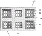
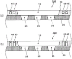
As shown in fig. 1(a) and (b), a vapor deposition mask 100 according to an embodiment of the present disclosure (hereinafter, referred to as a vapor deposition mask of the present disclosure) has the following configuration: the mask is formed by laminating a resin mask 20 having a plurality of resin mask openings 25 corresponding to a pattern to be vapor-deposited and a metal mask 10 having metal mask openings 15 such that the resin mask openings 25 and the metal mask openings 15 overlap each other. Fig. 1(a) is a schematic cross-sectional view showing an example of the vapor deposition mask 100 of the present disclosure, fig. 1(b) is a front view of the vapor deposition mask 100 of the present disclosure viewed from the metal mask side, and in the embodiment shown in fig. 1, the description of the rigidity adjusting portion 35 described later is omitted.
Forming a vapor deposition pattern on a vapor deposition object using a vapor deposition mask 100 having a laminated structure in which a resin mask 20 and a metal mask 10 are laminated is performed by: the vapor deposition mask 100 is disposed on one surface side of the vapor deposition object, and after the resin mask 20 of the vapor deposition mask 100 is brought into close contact with the vapor deposition object, the vapor deposition mask is discharged from the vapor deposition source, and the vapor deposition material passing through the vapor deposition mask openings 25 of the resin mask 20 is deposited on the vapor deposition object. Here, when the resin mask 20 of the vapor deposition mask 100 is brought into close contact with the vapor deposition object, if the close contact is low, in other words, if a gap is formed between the resin mask 20 of the vapor deposition mask 100 and the vapor deposition object, when the vapor deposition material discharged from the vapor deposition source passes through the resin mask opening 25, the vapor deposition patterns to be formed at a predetermined interval are connected to each other by the vapor deposition material entering through the gap, or the vapor deposition pattern has a large size. Therefore, in order to form a high-definition vapor deposition pattern, when the resin mask 20 of the vapor deposition mask 100 is brought into close contact with a vapor deposition object, it is desirable that the resin mask 20 of the vapor deposition mask 100 be in close contact with the vapor deposition object to such an extent that the adhesion is high, specifically, the above-described problem is not caused or the occurrence of the problem can be sufficiently suppressed.
Examples of a method for improving the adhesion between the resin mask 20 of the vapor deposition mask 100 and the vapor deposition object include: a method of arranging a magnetic material on the other surface side of the deposition target and attracting the deposition mask 100 and the deposition target by the magnetic force of the magnetic material; and a method of pressing the vapor deposition target from the other surface side of the vapor deposition target using a pressing member or the like to press the vapor deposition target into the vapor deposition mask 100.
However, in order to sufficiently improve the adhesion between the resin mask 20 of the vapor deposition mask 100 and the vapor deposition target, it is necessary to deform the shape of the resin mask 20 so as to follow the shape of the vapor deposition target by applying stress to the vapor deposition mask when the vapor deposition mask and the vapor deposition target are attracted by magnetic force, or by applying stress to the vapor deposition mask when the vapor deposition target is pressed against the vapor deposition mask side by a pressing member or the like (hereinafter, these stresses may be simply referred to as stress or stress applied to the vapor deposition mask). For example, when the vapor deposition mask 100 is warped, the resin mask 20 needs to be deformed to eliminate the warp and flatten the vapor deposition mask 100. However, the metal mask 10 made of a metal material has higher rigidity than the resin mask 20 made of a resin material, and the degree of deformation of the metal mask 10 when stress or the like is applied is smaller than that of the resin mask 20. In the vapor deposition mask 100 in which the metal mask 10 and the resin mask 20 are laminated, since the degree of deformation of the resin mask 20 is controlled by the degree of deformation of the metal mask 10, if the metal mask 10 cannot be sufficiently deformed, even if the vapor deposition mask 100 and the vapor deposition target are sucked as described above or the vapor deposition target is pressed against the vapor deposition mask 100 side, the shape of the resin mask 20 cannot be deformed so as to follow the shape of the vapor deposition target, and as a result, it is difficult to sufficiently improve the adhesion between the resin mask 20 of the vapor deposition mask 100 and the vapor deposition target.
In particular, in a vapor deposition mask having a laminated structure in which the resin mask 20 and the metal mask 10 having different thermal expansion coefficients are laminated, warpage (also referred to as curling) or the like is likely to occur in the vapor deposition mask 100 due to the difference in the thermal expansion coefficients, and if the metal mask 10 cannot be sufficiently deformed by stress, it is difficult to sufficiently improve the adhesion between the resin mask 20 of the vapor deposition mask 100 and the vapor deposition object.
In the vapor deposition mask 100 of the present disclosure, as shown in fig. 2 to 13, the metal mask 10 has 1 or a plurality of rigidity adjustment portions 35 that partially reduce the rigidity of the metal mask 10 at positions of the resin mask 20 that do not overlap with the resin mask openings 25. Note that fig. 2 to 4 and 10 to 13 show a rigidity adjustment unit placement region 30 (hereinafter, also referred to as a placement region) in which the rigidity adjustment unit 35 is placed. In fig. 2 to 4, the description of the rigidity adjustment section 35 is omitted, but in the same drawing, 1 or a plurality of rigidity adjustment sections 35 are disposed in the disposition area 30.
According to the vapor deposition mask 100 of the present disclosure, since the rigidity of the metal mask 10 is partially reduced, flexibility (also referred to as flexibility or stretchability) can be imparted to the metal mask 10, and the metal mask 10 can be easily deformed by stress or the like. Therefore, according to the vapor deposition mask 100 of the present disclosure, by partially reducing the rigidity of the metal mask 10, when the resin mask 20 of the vapor deposition mask 100 is brought into close contact with the vapor deposition object by using various methods, the shape of the resin mask 20 can be deformed so as to follow the shape of the vapor deposition object. That is, the adhesion between the resin mask 20 of the vapor deposition mask 100 and the object to be vapor deposited can be improved, and a high-definition vapor deposition pattern can be formed. Fig. 2 to 4 and 10 to 13 are plan views showing an example of the vapor deposition mask 100 of the present disclosure viewed from the metal mask 10 side. The respective configurations of the vapor deposition mask 100 of the present disclosure will be described below with reference to examples.
< resin mask >
As shown in fig. 1(b), the resin mask 20 is provided with a plurality of resin mask openings 25. In the illustrated embodiment, the opening shape of the resin mask opening 25 is rectangular, but the opening shape of the resin mask opening 25 is not particularly limited, and may be any shape as long as it corresponds to a pattern to be produced by vapor deposition. For example, the opening shape of the resin mask opening 25 may be a diamond shape or a polygonal shape, and may be a shape having a curvature such as a circle or an ellipse. The opening shape of the rectangular or polygonal shape is preferably an opening shape of the resin mask opening 25 in terms of increasing the light emitting area as compared with an opening shape having a curvature such as a circle or an ellipse.
The material of the resin mask 20 is not limited, and it is preferable to use a lightweight material that can form the resin mask openings 25 with high definition by laser processing or the like, and that has a small dimensional change rate and moisture absorption rate due to heat or time. Examples of such a material include polyimide resins, polyamide resins, polyamideimide resins, polyester resins, polyethylene resins, polyvinyl alcohol resins, polypropylene resins, polycarbonate resins, polystyrene resins, polyacrylonitrile resins, ethylene-vinyl acetate copolymer resins, ethylene-vinyl alcohol copolymer resins, ethylene-methacrylic acid copolymer resins, polyvinyl chloride resins, polyvinylidene chloride resins, cellophane, ionomer resins, and the like. Among the above-mentioned exemplary materials, a resin material having a thermal expansion coefficient of 16 ppm/DEG C or less is preferable, a resin material having a moisture absorption rate of 1.0% or less is preferable, and a resin material having both of these conditions is particularly preferable. By forming a resin mask using the resin material, the dimensional accuracy of the resin mask opening 25 can be improved, and the dimensional change rate and moisture absorption rate due to heat or time can be reduced.
The thickness of the resin mask 20 is not particularly limited, and in order to further improve the effect of suppressing the occurrence of the shadow, the thickness of the resin mask 20 is preferably 25 μm or less, and more preferably less than 10 μm. The preferable range of the lower limit is not particularly limited, and when the thickness of the resin mask 20 is less than 3 μm, defects such as pinholes are likely to occur, and the risk of deformation increases. In particular, the thickness of the resin mask 20 is 3 μm or more and less than 10 μm, preferably 4 μm or more and 8 μm or less, whereby the influence of the shadow at the time of forming a high-definition pattern exceeding 400ppi can be more effectively prevented. The resin mask 20 and the metal mask 10 described later may be bonded directly or via an adhesive layer, and when the resin mask 20 and the metal mask 10 are bonded via an adhesive layer, the total thickness of the resin mask 20 and the adhesive layer is preferably within the above-described preferred thickness range. The shadow is a phenomenon in which a part of the vapor deposition material discharged from the vapor deposition source collides with the inner wall surfaces of the metal mask opening of the metal mask and the resin mask opening of the resin mask and does not reach the vapor deposition target, thereby generating a non-vapor deposition portion having a film thickness smaller than the thickness of the target vapor deposition film.
The cross-sectional shape of the resin mask openings 25 is not particularly limited, and the opposing end faces of the resin mask forming the resin mask openings 25 may be substantially parallel to each other, but as shown in fig. 1(a), the cross-sectional shape of the resin mask openings 25 is preferably a shape that expands toward the vapor deposition source. In other words, it is preferable to have a tapered surface that expands toward the metal mask 10. The taper angle may be appropriately set in consideration of the thickness of the resin mask 20, and the angle formed by the straight line connecting the lower bottom tip of the resin mask opening of the resin mask and the upper bottom tip of the resin mask opening of the same resin mask and the bottom surface of the resin mask, in other words, the angle formed by the inner wall surface of the resin mask opening 25 and the surface of the resin mask 20 on the side not in contact with the metal mask 10 (in the illustrated embodiment, the upper surface of the resin mask) in the thickness direction cross section of the inner wall surface of the resin mask opening 25 constituting the resin mask 20 is preferably in the range of 5 ° to 85 °, more preferably in the range of 15 ° to 75 °, and even more preferably in the range of 25 ° to 65 °. In particular, in this range, an angle smaller than the deposition angle of the deposition machine used is also preferable. In the illustrated embodiment, the end surface on which the resin mask opening 25 is formed has a linear shape, but the present invention is not limited thereto, and may have a curved shape protruding outward, that is, the entire shape of the resin mask opening 25 may be bowl-shaped.
< Metal mask >
As shown in fig. 1(a), a metal mask 10 is laminated on one surface of a resin mask 20. The metal mask 10 is made of metal, and as shown in fig. 1(b), a metal mask opening 15 extending in the vertical or horizontal direction is provided. The arrangement example of the metal mask openings 15 is not particularly limited, and the metal mask openings 15 extending in the longitudinal direction and the lateral direction may be arranged in a plurality of rows in the longitudinal direction and the lateral direction, the metal mask openings 15 extending in the longitudinal direction may be arranged in a plurality of rows in the lateral direction, and the metal mask openings extending in the lateral direction may be arranged in a plurality of rows in the longitudinal direction. In addition, only 1 column may be arranged in the longitudinal direction or the lateral direction. The plurality of metal mask openings 15 may be arranged at random. In addition, the number of the metal mask openings 15 may be 1. The "longitudinal direction" and "lateral direction" in the present specification refer to the vertical direction and the lateral direction in the drawings, and may be any of the longitudinal direction and the width direction of a vapor deposition mask, a resin mask, or a metal mask. For example, the longitudinal direction of the vapor deposition mask, the resin mask, or the metal mask may be referred to as "vertical direction", or the width direction may be referred to as "vertical direction". In the present specification, a case where the vapor deposition mask has a rectangular shape in a plan view is described as an example, but other shapes such as a circle and a polygon such as a rhombus may be used. In this case, the longitudinal direction or the radial direction of the diagonal line, or any direction may be referred to as a "longitudinal direction", and a direction perpendicular to the "longitudinal direction" may be referred to as a "width direction" (also referred to as a "width direction").
(rigidity adjustment part)
As shown in fig. 2 to 13, the metal mask 10 includes 1 or more rigidity adjustment portions 35 that partially reduce the rigidity of the metal mask 10 at positions of the resin mask 20 that do not overlap with the resin mask openings 25. Specifically, 1 or more rigidity adjusting portions 35 for partially reducing the rigidity of the metal mask 10 are located in the arrangement region 30 shown in fig. 2 to 4 and 10 to 13.
The rigidity of the metal mask referred to in the present specification means a degree at which the metal mask is easily deformed (sometimes referred to as displacement or displacement amount) in a region to which a load is applied when a certain load is applied to the vapor deposition mask, and the rigidity of the metal mask decreases as the rigidity decreases, in other words, as the displacement amount increases. The rigidity of the metal mask can be calculated by the following equation (1). Specifically, the rigidity (k) of the metal mask can be calculated by applying a vertical load (F) to a predetermined region of the vapor deposition mask 100 and measuring the displacement amount (δ) of the metal mask in the region to which the vertical load (F) is applied. The amount of displacement (δ) of the metal mask can be measured using, for example, a laser displacement meter. Further, as a method of applying a vertical load, for example, a method of placing a weight having a given mass on a given area, a method of using a machine for applying a load, or the like,
k=F/δ···(1)。
in the vapor deposition mask 100 of the present disclosure, the rigidity of the metal mask 10 in the arrangement region 30 can be made lower than the rigidity of the region where the rigidity adjustment portion 35 is not arranged by positioning the rigidity adjustment portion 35 in the arrangement region 30. That is, the metal mask 10 having the rigidity adjustment portion 35 can provide flexibility to the metal mask. According to the vapor deposition mask 100 of the present disclosure, when the vapor deposition mask 100 and the vapor deposition object are brought into close contact with each other so that the resin mask 20 faces the vapor deposition object by using stress due to flexibility imparted to the metal mask 10, the shape of the resin mask 20 can be deformed to such an extent that no gap is generated between the vapor deposition objects. In other words, the shape of the resin mask 20 can follow the shape of the vapor deposition target. That is, the adhesion between the vapor deposition mask 100 and the vapor deposition object can be improved.
The method of partially reducing the rigidity of the metal mask 10 by the rigidity adjustment unit 35 is not particularly limited, and can be realized by various methods as exemplified below. In addition, the rigidity of the metal mask may be partially reduced by other methods.
(i) For example, by providing 1 or more through holes 40 as the rigidity adjustment portion 35 penetrating the metal mask 10 in a predetermined region of the metal mask that does not overlap the resin mask opening 25 in the thickness direction, that is, a region where the rigidity is desired to be reduced, the rigidity of the metal mask 10 including the peripheral region of the through holes 40 can be reduced (see fig. 5(b), (c), and 9 (b)).
The through-hole 40 is a hole penetrating only the metal mask 10. The method for forming the through hole 40 is not particularly limited, and etching, cutting, and the like may be appropriately selected.
(ii) Further, by providing 1 or more concave portions 45 as the rigidity adjusting portion 35 which do not penetrate the metal mask 10 in a predetermined region of the metal mask which does not overlap the resin mask opening 25 in the thickness direction, that is, a region where the rigidity is desired to be reduced, the rigidity of the metal mask 10 including the peripheral region of the concave portions 45 can also be reduced (see fig. 5 and 9).
The method for forming the concave portion 45 is not particularly limited, and etching, cutting, and the like may be appropriately selected. The depth of the recess 45 is not particularly limited, and may be appropriately set in consideration of the thickness of the metal mask 10 and the degree of reduction in rigidity. For example, the thickness is in the range of 1 μm to 100 μm.
Hereinafter, unless otherwise specified, the reference to the rigidity adjustment portion 35 means that the through hole 40 and the concave portion 45 as the rigidity adjustment portion 35 are included.
The shape of the through-hole 40 and the concave portion 45 as the rigidity adjustment portion 35 is not particularly limited, and examples of the shape of the vapor deposition mask 100 when viewed from the side of the metal mask 10 include a polygonal shape such as a triangular shape, a rectangular shape, a rhombic shape, a trapezoidal shape, a pentagonal shape, and a hexagonal shape, a circular shape, an elliptical shape, and a shape in which corners of the polygonal shape have curvatures. Further, a combination of these shapes may be used. Fig. 26 is a diagram showing an example of a plan view of the aggregate of the "rigidity adjustment unit" from the metal mask 10 side. In fig. 26, the closed region may be the rigidity adjustment portion 35, or the closed region may be a non-through hole or a non-recessed portion.
The size of the through hole 40 and the concave portion 45 as the rigidity adjustment portion 35 is not particularly limited, and may be appropriately set according to the position of the rigidity adjustment portion 35. For example, the area of the opening region of the rigidity adjustment portion 35 when viewed from the metal mask side in plan view may be larger than, smaller than, or the same as the area of the opening region of the metal mask opening 15. It should be noted that consideration is given toIn order to facilitate adjustment of the rigidity of the metal mask 10, the area of the opening region of 1 rigidity adjustment portion 35 is preferably smaller than the area of the opening region of the metal mask opening 15. For example, the area of the opening region of 1 rigidity adjustment portion 35, in other words, the area of the opening region of 1 through hole 40 and 1 recess 45 is preferably 1 μm 2 Above and 1 × 10 12 μm 2 Within the following ranges.
The opening widths of the through holes 40 and the concave portions 45 as the rigidity adjustment portions 35 are not particularly limited, and for example, the opening widths of the rigidity adjustment portions 35 in the vapor deposition mask longitudinal direction and the width direction when viewed from the metal mask side may be larger than, smaller than, or the same as the opening widths of the vapor deposition mask longitudinal direction and the width direction of the metal mask openings 15. The opening width of the rigidity adjustment portion 35 may be appropriately set according to the position of the through hole 40, and for example, when the metal mask 10 has a plurality of metal mask openings 15 and the rigidity adjustment portion 35 is positioned between adjacent metal mask openings 15 in the longitudinal direction of the vapor deposition mask, the opening width in the longitudinal direction when the rigidity adjustment portion 35 is viewed from the metal mask 10 side may be smaller than the interval in the longitudinal direction of the adjacent metal mask openings 15. The same applies to the case where the rigidity adjustment portion 35 is positioned between the metal mask openings 15 adjacent in the width direction of the vapor deposition mask.
The total area of the opening regions of the through holes 40 and the recesses 45, which are the rigidity adjustment portions 35 when the vapor deposition mask 100 of the present disclosure is viewed from the metal mask 10 side, is preferably 3% or more, more preferably 10% or more, and particularly preferably 30% or more, where the area of the metal mask effective region is 100% when the metal mask, which is assumed to have no rigidity adjustment portions 35, that is, the metal mask having only the metal mask openings 15, is viewed from the metal mask side. The area of the metal mask effective region referred to herein is a partial surface area where a metal portion exists when the vapor deposition mask is viewed from the side of the metal mask 10 in plan view. By setting the ratio of the area of the opening region of the through hole 40 and the recess 45 as the rigidity adjustment portion 35 to the above-described preferable range, flexibility can be imparted to the metal mask 10 while maintaining the rigidity of the entire metal mask 10, and adhesion between the resin mask 20 of the vapor deposition mask 100 and the vapor deposition target can be further improved. The upper limit value of the total area of the opening regions of the rigidity adjustment portion 35 is not particularly limited, but is preferably 95% or less, more preferably 90% or less, and particularly preferably 70% or less, in view of the rigidity of the metal mask.
The rigidity adjusting portion 35 described above, that is, the through holes 40 and the concave portions 45 as the rigidity adjusting portion, may be arranged at any position or pitch without any particular limitation, and may be arranged regularly or randomly. Further, as an example of the pitch between the adjacent rigidity adjustment portions 35, 1 μm or more and 2 × 10 6 A range of μm or less.
In the case where a plurality of rigidity adjustment portions 35 are provided in the metal mask 10, the area of the opening region of each rigidity adjustment portion 35 may be the same or different. The same applies to the pitch. Further, the through-hole 40 and the concave portion 45 as the rigidity adjustment portion 35 may be used in combination.
(region for disposing rigidity adjustment part)
The arrangement region in which the rigidity adjustment portion 35 is arranged is not particularly limited, and may be appropriately arranged at a position where the rigidity of the metal mask 10 is expected to be reduced, that is, a position where the adhesion between the resin mask 20 and the vapor deposition object is likely to be insufficient. In the metal mask 10 of the preferred embodiment, as shown in fig. 2 to 4 and 10 to 13, the arrangement region 30 is located around the metal mask opening 15, and 1 or more rigidity adjustment portions 35 are arranged in the arrangement region 30. According to the vapor deposition mask 100 of the present disclosure including the metal mask 10 of the preferred embodiment, the adhesion between the resin mask 20 of the vapor deposition mask 100 and the vapor deposition target can be extremely improved, and a higher-definition vapor deposition pattern can be formed.
In the vapor deposition mask 100 of the embodiment shown in fig. 2 and 3, the metal mask 10 has a plurality of metal mask openings 15, and the disposition region 30 is located at a position surrounding the metal mask openings 15. In the embodiment shown in fig. 2, the position of the placement region 30 is set so as to surround the metal mask opening 15 and overlap the outer edge of the metal mask opening 15 with the outer edge of the placement region 30. In the embodiment shown in fig. 3, the position of the placement region 30 is set so as to surround at least 1 metal mask opening 15 of the plurality of metal mask openings 15 and overlap the outer edge of the metal mask opening 15 with the outer edge of the placement region 30. In the embodiment shown in fig. 4, the position of the placement region 30 is provided so as to surround the metal mask opening 15 and prevent the outer edge of the metal mask opening 15 from overlapping the outer edge of the placement region 30, in other words, the position of the placement region 30 is provided at a predetermined interval from the outer edge of the metal mask opening 15.
Fig. 5 and 9 are enlarged front views showing examples of the arrangement of the rigidity adjusting section 35 arranged in the arrangement region 30 (enlarged front views showing examples of regions indicated by reference symbol X in fig. 1 b), fig. 6 is an example of a-a schematic cross-sectional view in fig. 5 a, fig. 7 a and b are examples of a-a schematic cross-sectional views in fig. 5 b, and fig. 8 a and b are examples of a-a schematic cross-sectional views in fig. 5 c. In the embodiment shown in fig. 5(a), 1 metal mask opening 15 is surrounded by 1 continuous concave portion 45 serving as the rigidity adjustment portion 35 so that the outer edge of the metal mask opening 15 overlaps the outer edge of the rigidity adjustment portion 35. In the embodiment shown in fig. 5(b), 1 metal mask aperture 15 is surrounded by an aggregate of the plurality of rigidity adjusters 35 so that the outer edges of the metal mask apertures 15 do not overlap the outer edges of the rigidity adjusters 35. The rigidity adjustment portion 35 of the embodiment shown in fig. 5(b) may be any of the through hole 40 and the concave portion 45. In the embodiment shown in fig. 5(c), 1 metal mask opening 15 is surrounded by 1 continuous rigidity adjustment portion 35 so that the outer edge of the metal mask opening 15 does not overlap the outer edge of the rigidity adjustment portion 35. The rigidity adjustment portion 35 shown in fig. 5(c) may be a continuous 1 through-hole 40 or a continuous 1 recessed portion 45. Further, a combination of these methods may be employed.
A vapor deposition mask 100 according to a preferred embodiment is as follows: the metal mask opening 15 is surrounded by 1 or more rigidity adjusting portions 35 so that the outer edge of the metal mask opening 15 does not overlap the outer edge of the placement region 30, in other words, so that the outer edge of the metal mask opening 15 does not overlap the outer edge of the rigidity adjusting portion 35 (the modes shown in fig. 5(b) and (c)). According to the vapor deposition mask 100 of the preferred embodiment, when a magnetic material is disposed on the other surface side of the vapor deposition object and the vapor deposition mask 100 and the vapor deposition object are attracted by the magnetic force of the magnetic material, the adhesion between the vapor deposition mask 100 and the vapor deposition object at the position overlapping the outer peripheral end portion of the metal mask opening 15 can be further improved.
The rigidity adjusting section 35 shown in each figure may be divided into a plurality of rigidity adjusting sections 35. Fig. 9(a) shows a mode in which 1 rigid adjustment unit 35 shown in fig. 5(a) is divided into a plurality of rigid adjustment units 35, and fig. 9(b) shows a mode in which 1 rigid adjustment unit 35 shown in fig. 5(c) is divided into a plurality of rigid adjustment units 35. In addition, the modes shown in the respective drawings may be appropriately combined.
In the vapor deposition mask 100 of the embodiment shown in fig. 10(a), (b) and 11(a), (b), the metal mask 10 has a plurality of metal mask openings 15, and the position of the placement region 30 is provided so as to surround the entirety of the plurality of metal mask openings 15. In the embodiment shown in fig. 10, the outer edge of the metal mask opening 15 overlaps the outer edge of the placement region 30, and in the embodiment shown in fig. 11, the outer edge of the placement region 30 is located at a predetermined interval from the outer edge of the metal mask opening 15. In the embodiment shown in fig. 10 and 11, a plurality of rigidity adjustment portions 35 are arranged in the arrangement region 30, but in the embodiment shown in fig. 10, the entire arrangement region 30 may be defined as the recess 45. In the embodiment shown in fig. 11, the entire arrangement region 30 may be the through hole 40 or the recess 45.
In the vapor deposition mask 100 of the embodiment shown in fig. 12, the metal mask 10 has a plurality of metal mask openings 15, and the arrangement region 30 is located at least in a part between the adjacent metal mask openings 15. In the embodiment shown in fig. 12, a plurality of rigidity adjustment portions 35 are arranged in the arrangement region 30, but in the embodiment shown in fig. 12, the entire arrangement region 30 may be a through hole 40 or a recess 45.
In the vapor deposition mask 100 of the embodiment shown in fig. 13(a) and (b), the metal mask 10 has only 1 metal mask opening 15, and the position of the placement region 30 is provided so as to surround the 1 metal mask opening 15. In the embodiment shown in fig. 13(a), the outer edge of the metal mask opening 15 overlaps the outer edge of the placement region 30, and in the embodiment shown in fig. 13(b), the outer edge of the placement region 30 is located at a predetermined interval from the outer edge of the metal mask opening 15. In view of the fact that the frame and the vapor deposition mask are usually fixed to the outer periphery of the vapor deposition mask, it is preferable that the outer edge of the metal mask 10 not overlap the outer edge of the placement region 30. That is, the concave portion 45 is preferably not located at a portion overlapping with the outer edge of the metal mask. In the embodiment shown in fig. 13, a plurality of rigidity adjustment portions 35 are arranged in the arrangement region 30, but in the embodiment shown in fig. 13(a), the entire arrangement region 30 may be defined as the recess 45, and in the embodiment shown in fig. 13(b), the entire arrangement region 30 may be defined as the through hole 40 or the recess 45. That is, the entire arrangement region may be used as the rigidity adjustment portion 35, that is, 1 continuous through hole 40 and recess 45 may surround 1 metal mask opening 15 (see fig. 5(a) and (c)). Instead of the illustrated embodiment, the rigidity adjustment unit 35 may be disposed only in a part of the disposition region 30, for example, in the vicinity of the corners of the metal mask (not illustrated).
In the vapor deposition mask 100 of a preferred embodiment, when the metal mask 10 has only 1 metal mask opening 15, the placement region 30 surrounds the 1 metal mask opening 15 and is located at a predetermined interval from the outer edge of the metal mask opening 15, and the entire placement region is the 1 rigidity adjustment portion 35 (not shown), or a plurality of rigidity adjustment portions 35 (not shown) are disposed along the placement region 30. According to the vapor deposition mask 100 of the preferred embodiment, when a magnetic material is disposed on the other surface side of the vapor deposition object and the vapor deposition mask 100 and the vapor deposition object are attracted by the magnetic force of the magnetic material, the adhesion between the vapor deposition mask 100 and the vapor deposition object can be further improved at the position where the metal mask openings 15 overlap the outer peripheral end portion.
Fig. 16 is a front view showing a state in which the size of a gap which is generated between the resin mask 20 of the vapor deposition mask 100 and the deposition target is classified into stages, which is generated when the metal mask 10 has a plurality of metal mask openings 15 and the rigidity adjusting portion 35 is not positioned in the metal mask 10, and the gap tends to be easily generated in the order of "C" > "B" > "a".
Therefore, in the vapor deposition mask 100 of the preferred embodiment, the rigidity adjustment portion 35 is preferably located in the peripheral region of the metal mask opening 15 corresponding to the position (level "C") where the occurrence of the gap is expected to increase as shown in fig. 16, more preferably, the rigidity adjustment portion 35 is located in the peripheral region of the metal mask opening 15 corresponding to the level "C" and the level "B", and particularly, the rigidity adjustment portion 35 is preferably located in the peripheral region of all the metal mask openings 15. Further, the area of the opening region of the rigidity adjustment portion 35, the proportion of the rigidity adjustment portion, and the like may be changed for each region, and the rigidity of the metal mask 10 may be changed stepwise. For example, when the peripheral region including the horizontal "C" is the 1 st region, the peripheral region including the horizontal "B" is the 2 nd region, the peripheral region including the horizontal "a" is the 3 rd region, and the areas of the 1 st region to the 3 rd region are made the same, the rigidity of the metal mask can be adjusted for each region by changing the ratio of the rigidity adjusting portion 35 in each region. For example, the rigidity of the metal mask can be adjusted for each adjustment region by setting the proportion of the rigidity adjustment portion 35 in the 1 st region to be larger than the proportion of the rigidity adjustment portion in the 2 nd region, and by not positioning the rigidity adjustment portion 35 in the 3 rd region, or by setting the proportion of the rigidity adjustment portion 35 in the 2 nd region to be smaller than the proportion of the rigidity adjustment portion in the 2 nd region.
The material of the metal mask 10 is not particularly limited, and a conventionally known material can be suitably selected and used in the field of vapor deposition masks, and examples thereof include metal materials such as stainless steel, iron-nickel alloys, and aluminum alloys. Among them, invar alloy materials, which are iron-nickel alloys, are less deformed by heat and therefore can be suitably used.
The thickness of the metal mask 10 is not particularly limited, and is preferably 100 μm or less, more preferably 50 μm or less, and particularly preferably 35 μm or less, in order to more effectively prevent the occurrence of a shadow. Further, when the thickness is thinner than 5 μm, the risk of breakage or deformation increases, and handling tends to be difficult.
In the embodiment shown in each drawing, the shape of the opening of the metal mask opening 15 in a plan view is rectangular, but the opening shape is not particularly limited, and the opening shape of the metal mask opening 15 may be any shape such as a trapezoidal shape or a circular shape.
The sectional shape of the metal mask opening 15 formed in the metal mask 10 is not particularly limited, but is preferably a shape that expands toward the vapor deposition source as shown in fig. 1 (a). More specifically, the angle formed by the bottom surface of the metal mask opening 15 of the metal mask 10, the straight line connecting the bottom surface of the metal mask opening 15 of the same metal mask 10, and the top surface of the metal mask opening 15, in other words, the angle formed by the inner wall surface of the metal mask opening 15 and the surface of the metal mask 10 on the side contacting the resin mask 20 (in the illustrated embodiment, the top surface of the metal mask) in the thickness direction cross section of the inner wall surface of the metal mask opening 15 constituting the metal mask 10, is preferably in the range of 5 ° to 85 °, more preferably in the range of 15 ° to 80 °, and even more preferably in the range of 25 ° to 65 °. In particular, an angle smaller than the deposition angle of the deposition machine used is also preferable in this range.
The opening space of the metal mask opening 15 may be partitioned by a bridge (not shown).
The method of laminating the metal mask 10 on the resin mask is not particularly limited, and the resin mask 20 and the metal mask 10 may be bonded to each other with various adhesives or may be self-adhesive. The resin mask 20 and the metal mask 10 may have the same size or different sizes. In consideration of the optional fixing to the frame, it is preferable that the size of the resin mask 20 is smaller than that of the metal mask 10, and the metal mask 10 is preferably in a state in which the outer peripheral portion thereof is exposed, whereby the metal mask 10 and the frame can be easily fixed.
Next, as more preferable specific examples of the vapor deposition mask of the present disclosure, embodiments (a) and (B) will be described as examples. In fig. 17 to 22, the description of the rigidity adjusting portion 35 and the arrangement region 30 is omitted, but the configurations described above can be appropriately used for the rigidity adjusting portion 35 and the arrangement region 30.
< vapor deposition mask of embodiment (A) >
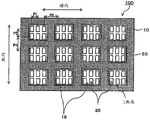
As shown in fig. 17, a vapor deposition mask 100 according to embodiment (a) is a vapor deposition mask for simultaneously forming vapor deposition patterns for a plurality of screens, and includes a resin mask 20 and a metal mask 10 stacked on one surface of the resin mask 20 and having a plurality of metal mask opening portions 15, the resin mask 20 having resin mask opening portions 25 for forming a plurality of screens, and each of the metal mask opening portions 15 being provided at a position overlapping at least 1 screen as a whole. Further, the metal mask 10 of the vapor deposition mask 100 according to embodiment (a) has 1 or more rigidity adjustment portions 35 that partially reduce the rigidity of the metal mask 10 at positions of the resin mask 20 that do not overlap with the resin mask openings 25, and thus, when the vapor deposition mask according to embodiment (a) is brought into close contact with a vapor deposition object, the adhesion between the resin mask 20 and the vapor deposition object can be improved. In the metal mask 10 of the vapor deposition mask 100 according to embodiment (a), the rigidity adjustment portion 35 is preferably positioned between at least 1 screen among the screens, at a position surrounding at least 1 screen, at a position surrounding the entirety of a plurality of screens, or at a position surrounding the entirety of all the screens.
The vapor deposition mask 100 according to embodiment (a) is a vapor deposition mask for simultaneously forming vapor deposition patterns for a plurality of screens, and vapor deposition patterns corresponding to a plurality of products can be simultaneously formed using 1 vapor deposition mask 100. The "resin mask opening" in the vapor deposition mask of embodiment (a) refers to a pattern to be produced using the vapor deposition mask 100 of embodiment (a), and, for example, when the vapor deposition mask is used for forming an organic layer of an organic EL display, the shape of the resin mask opening 25 is the shape of the organic layer. Further, "1 screen" is constituted by an aggregate of the resin mask openings 25 corresponding to 1 product, and in the case where the 1 product is an organic EL display, an aggregate of organic layers necessary for forming 1 organic EL display, that is, an aggregate of the resin mask openings 25 of the organic layers becomes "1 screen". In the vapor deposition mask 100 according to embodiment (a), the above-described "1 screen" is arranged on the resin mask 20 at a predetermined interval so as to form vapor deposition patterns of a plurality of screens at the same time. That is, the resin mask 20 is provided with a resin mask opening 25 necessary for forming a plurality of screens.
The vapor deposition mask according to embodiment (a) is provided with a metal mask 10 having a plurality of metal mask openings 15 on one surface of a resin mask, and each of the metal mask openings is provided at a position overlapping at least 1 screen as a whole. In other words, between the resin mask openings 25 necessary for forming 1 screen, there is no metal line portion having the same length as the longitudinal length of the metal mask opening 15 and the same thickness as the metal mask 10 between the resin mask openings 25 adjacent in the lateral direction, and there is no metal line portion having the same length as the lateral length of the metal mask opening 15 and the same thickness as the metal mask 10 between the resin mask openings 25 adjacent in the longitudinal direction. Hereinafter, a metal line portion having the same length as the longitudinal length of the metal mask opening 15 and the same thickness as the metal mask 10 and a metal line portion having the same length as the lateral length of the metal mask opening 15 and the same thickness as the metal mask 10 may be collectively simply referred to as a metal line portion.
According to the vapor deposition mask 100 of embodiment (a), even when the size of the resin mask openings 25 necessary for 1 screen and the pitch between the resin mask openings 25 constituting 1 screen are made small, for example, in order to form a screen exceeding 400ppi, the size of the resin mask openings 25 and the pitch between the resin mask openings 25 are made extremely small, and thus, it is possible to prevent interference caused by the metal wire portions and form a high-definition image. In addition, when 1 screen is divided by a plurality of metal mask openings, in other words, when there are metal line portions having the same thickness as the metal mask 10 between the resin mask openings 25 constituting 1 screen, as the pitch between the resin mask openings 25 constituting 1 screen becomes narrower, the metal line portions existing between the resin mask openings 25 become an obstacle when forming a vapor deposition pattern on a vapor deposition object, and it is difficult to form a high-definition vapor deposition pattern. In other words, when a metal line portion having the same thickness as that of the metal mask 10 is present between the resin mask openings 25 constituting 1 screen, the metal line portion causes a shadow when formed as a framed vapor deposition mask, and it is difficult to form a high-definition screen.
Next, an example of the resin mask opening 25 constituting 1 screen will be described with reference to fig. 17 to 20. In the illustrated embodiment, the area enclosed by the broken line is 1 screen. In the illustrated embodiment, for convenience of explanation, the aggregate of a small number of resin mask openings 25 is 1 screen, but the present invention is not limited to this embodiment, and for example, when 1 resin mask opening 25 is 1 pixel, resin mask openings 25 of millions of pixels may be present on 1 screen.
In the embodiment shown in fig. 17, 1 screen is constituted by an aggregate of resin mask openings 25 in which a plurality of resin mask openings 25 are provided in the vertical and horizontal directions. In the embodiment shown in fig. 18, 1 screen is constituted by an aggregate of resin mask openings 25 in which a plurality of resin mask openings 25 are provided in the lateral direction. In the embodiment shown in fig. 19, 1 screen is formed by an aggregate of resin mask openings 25 in which a plurality of resin mask openings 25 are provided in the vertical direction. In fig. 17 to 19, a metal mask opening 15 is provided at a position overlapping the entire 1 screen.
As described above, the metal mask opening 15 may be provided at a position overlapping only 1 screen, or may be provided at a position overlapping 2 or more screens as a whole, as shown in fig. 20(a) and (b). In fig. 20(a), in the resin mask 20 shown in fig. 17, a metal mask opening 15 is provided at a position that overlaps with 2 screens continuing in the lateral direction. In fig. 20(b), a metal mask opening 15 is provided at a position overlapping the entire 3 vertically continuous screens.
Next, the pitch between the resin mask openings 25 constituting 1 screen and the pitch between screens will be described by taking the mode shown in fig. 17 as an example. The pitch between the resin mask openings 25 constituting 1 screen and the size of the resin mask openings 25 are not particularly limited, and can be appropriately set according to the pattern to be produced by vapor deposition. For example, when a 400ppi high-definition vapor deposition pattern is formed, the pitch in the lateral direction (P1) and the pitch in the vertical direction (P2) of the adjacent resin mask openings 25 in the resin mask openings 25 constituting 1 screen are about 60 μm. In addition, the size of the opening of the resin mask is 500 μm as an example 2 Above and 1000 μm 2 Within the following ranges. The 1 resin mask opening 25 is not limited to correspond to 1 pixel, and for example, a plurality of pixels may be arranged in a pixel array to form 1 resin mask opening 25.
The inter-screen horizontal pitch (P3) and vertical pitch (P4) are also not particularly limited, and as shown in fig. 17, when 1 metal mask opening 15 is provided at a position overlapping the entire 1 screen, a metal line portion exists between the screens. Therefore, when the vertical pitch (P4) and the horizontal pitch (P3) between the screens are smaller than or substantially equal to the vertical pitch (P2) and the horizontal pitch (P1) of the resin mask openings 25 provided in 1 screen, the metal line portions existing between the screens are easily disconnected. In particular, when the rigidity adjustment unit 35 is positioned between the screens, there is a high risk of disconnection of the metal wire portion. Therefore, in consideration of this point, the pitch between screens (P3, P4) is preferably wider than the pitch between the resin mask openings 25 constituting 1 screen (P1, P2). The pitch (P3, P4) between screens is, for example, in the range of 1mm to 100 mm. The pitch between screens is a pitch between openings of the resin mask adjacent to each other on 1 screen and another screen adjacent to the 1 screen. This is also true for the pitch between the resin mask openings 25 and the pitch between screens of the deposition mask in embodiment (B) to be described later.
As shown in fig. 20, when 1 metal mask opening 15 is provided at a position overlapping two or more screens as a whole, there is no metal line portion constituting the inner wall surface of the metal mask opening between the screens provided in the 1 metal mask opening 15. Therefore, in this case, the pitch between two or more screens provided at the position overlapping with 1 metal mask opening 15 may be substantially the same as the pitch between the resin mask openings 25 constituting 1 screen.
Further, a groove (not shown) extending in the longitudinal direction or the lateral direction of the resin mask 20 may be formed in the resin mask 20. When heat is applied during vapor deposition, the resin mask 20 thermally expands, and thus the size and position of the resin mask opening 25 may change, but the formation of the grooves can absorb the expansion of the resin mask, and can prevent the accumulation of thermal expansion occurring at various positions of the resin mask, thereby expanding the entire resin mask 20 in a predetermined direction and changing the size and position of the resin mask opening 25. The positions where the grooves are formed are not limited, and may be provided between the resin mask openings 25 constituting 1 screen or at positions overlapping the resin mask openings 25, but are preferably provided between screens. The grooves may be provided only on one surface of the resin mask, for example, on the surface on the side contacting the metal mask, or may be provided only on the surface on the side not contacting the metal mask. Or may be provided on both sides of the resin mask 20.
Further, a groove extending in the vertical direction between adjacent screens may be provided, or a groove extending in the horizontal direction between adjacent screens may be formed. In addition, grooves may be formed in a combination thereof.
The depth and width of the groove are not particularly limited, but when the depth of the groove is too deep or the width is too wide, the rigidity of the resin mask 20 tends to decrease, and thus it is necessary to set the depth and width in consideration of this point. The cross-sectional shape of the groove is not particularly limited, and may be arbitrarily selected in consideration of the processing method, for example, a U-shape or a V-shape. The same applies to the vapor deposition mask of embodiment (B).
< vapor deposition mask of embodiment (B) >
Next, a vapor deposition mask of embodiment (B) will be described. As shown in fig. 21, the vapor deposition mask according to embodiment (B) is formed by laminating a metal mask 10 having 1 metal mask opening 15 on one surface of a resin mask 20 having a plurality of resin mask openings 25 corresponding to a pattern to be vapor deposited, and all of the plurality of resin mask openings 25 are provided at positions overlapping with the 1 metal mask opening 15 having the metal mask 10. Further, the metal mask 10 of the vapor deposition mask 100 according to embodiment (B) has 1 or more rigidity adjustment portions 35 that partially reduce the rigidity of the metal mask 10 at positions of the resin mask 20 that do not overlap with the resin mask openings 25, and thus, when the vapor deposition mask according to embodiment (a) is brought into close contact with a vapor deposition object, the adhesion between the resin mask 20 and the vapor deposition object can be improved. In the metal mask 10 of the vapor deposition mask 100 according to embodiment (B), the rigidity adjustment portion 35 is preferably located at a position surrounding 1 metal mask opening 15.
The resin mask openings 25 in the vapor deposition mask according to embodiment (B) are resin mask openings necessary for forming a vapor deposition pattern on a vapor deposition target, and resin mask openings unnecessary for forming a vapor deposition pattern on a vapor deposition target may be provided at positions not overlapping 1 metal mask opening 15. Fig. 21 is a front view of a vapor deposition mask showing an example of the vapor deposition mask of embodiment (B) as viewed from the metal mask side.
In the vapor deposition mask 100 according to embodiment (B), the metal mask 10 having one metal mask opening 15 is provided on the resin mask 20 having the plurality of resin mask openings 25, and all of the plurality of resin mask openings 25 are provided at positions overlapping with the one metal mask opening 15. In the vapor deposition mask 100 of embodiment (B) having this configuration, since there are no metal line portions between the resin mask openings 25, which are equal to or thicker than the thickness of the metal mask, a high-definition vapor deposition pattern can be formed in accordance with the size of the resin mask openings 25 provided in the resin mask 20 without being disturbed by the metal line portions, as described in the vapor deposition mask of embodiment (a).
Further, according to the vapor deposition mask of embodiment (B), even when the thickness of the metal mask 10 is increased, the thickness of the metal mask 10 can be increased to sufficiently satisfy durability and operability, and durability and operability can be improved while forming a high-definition vapor deposition pattern.
The resin mask 20 of the vapor deposition mask according to embodiment (B) is made of a resin, and as shown in fig. 6, a plurality of resin mask openings 25 corresponding to a pattern to be vapor deposited are provided at positions overlapping one metal mask opening 15. The resin mask openings 25 correspond to a pattern to be formed by vapor deposition, and a vapor deposition pattern corresponding to the resin mask openings 25 is formed in the vapor deposition target by passing the vapor deposition material discharged from the vapor deposition source through the openings 25. In the illustrated embodiment, a plurality of resin mask openings are arranged in a row in the vertical direction, but may be arranged only in the vertical direction or the horizontal direction.
The "1 screen" in the vapor deposition mask 100 according to embodiment (B) refers to an aggregate of the resin mask openings 25 corresponding to one product, and in the case where the one product is an organic EL display, an aggregate of organic layers necessary for forming the one organic EL display, that is, an aggregate of the resin mask openings 25 serving as organic layers is "1 screen". The vapor deposition mask according to embodiment (B) may be configured by only "1 screen", or the "1 screen" may be arranged in a plurality of screens, and when the "1 screen" is arranged in a plurality of screens, it is preferable that the resin mask openings 25 be provided at predetermined intervals for each screen unit (see fig. 17 of the vapor deposition mask according to embodiment (a)). The mode of "1 screen" is not particularly limited, and for example, when one resin mask opening 25 is 1 pixel, 1 screen may be configured by millions of resin mask openings 25.
The metal mask 10 in the vapor deposition mask 100 according to embodiment (B) is made of metal and has 1 metal mask opening 15. In the vapor deposition mask 100 according to embodiment (B), the 1 metal mask opening 15 is disposed at a position overlapping with all the resin mask openings 25 when viewed from the front of the metal mask 10, that is, at a position where all the resin mask openings 25 disposed in the resin mask 20 are visible.
The metal portion constituting the metal mask 10, that is, the portion other than the 1 metal mask opening 15 may be provided along the outer edge of the vapor deposition mask 100 as shown in fig. 21, or the metal mask 10 may be smaller in size than the resin mask 20 as shown in fig. 22 so that the outer peripheral portion of the resin mask 20 is exposed. The size of the metal mask 10 may be larger than that of the resin mask 20, and a part of the metal portion may protrude outward in the lateral direction or outward in the longitudinal direction of the resin mask. In any case, the size of 1 metal mask opening 15 is smaller than the size of the resin mask 20.
The lateral width (W1) and the vertical width (W2) of the metal portion forming the wall surface of the 1 metal mask opening 15 of the metal mask 10 shown in fig. 21 are not particularly limited, but the durability and the handling property tend to be reduced as the widths of W1 and W2 become narrower. Therefore, W1 and W2 are preferably wide enough to satisfy durability and operability. The appropriate width can be appropriately set according to the thickness of the metal mask 10, but as an example of a preferable width, both W1 and W2 are in the range of 1mm to 100mm, as in the metal mask of embodiment (a).
< vapor deposition mask of other embodiment (i) >
In the vapor deposition mask of the above-described embodiment, the through-holes 40 or the recesses 45 are provided as the rigidity adjustment portions 35 in the metal mask 10, whereby the rigidity of the metal mask including the peripheral regions of the through-holes 40 or the recesses 45 is reduced, but instead of this, as shown in fig. 14, the metal reinforcements 17 serving as the rigidity adjustment portions 35 are provided on the surface of the metal mask 10 not overlapping the resin mask openings 25 in the thickness direction, whereby the rigidity of the metal mask 10 including the peripheral regions of the metal reinforcements is improved.
That is, the vapor deposition mask of the other embodiment (i) is different from the vapor deposition mask of the above-described embodiment in that the rigidity of the metal mask in the peripheral region including the rigidity adjustment portion 35 is increased by the metal reinforcement 17 as the rigidity adjustment portion 35, compared to the vapor deposition mask of the above-described embodiment in which the rigidity of the metal mask in the peripheral region including the rigidity adjustment portion 35 is decreased by the through holes 40 and the concave portions 45 as the rigidity adjustment portion 35. Note that, unless otherwise specified, the vapor deposition mask of the other embodiment (i) can be used by appropriately selecting the configuration of the vapor deposition mask of the embodiment described above.
The thickness of the metal mask 10 in the vapor deposition mask according to the other embodiment (i) is not particularly limited, and may be a thickness enough to provide flexibility. For example, it is 35 μm or less, preferably 25 μm or less, and more preferably 15 μm or less.
Examples of the metal reinforcement 17 include: a metal plate provided on the metal mask 10, a metal plating layer formed on the metal mask, and the like.
The position of the metal reinforcement 17 is not particularly limited, and the metal reinforcement 17 may be appropriately disposed in the region indicated by reference numeral 10 in fig. 2 to 4 and 10 to 13, for example.
The thickness of the metal stiffener 17 is not particularly limited, and may be set as appropriate according to the degree of improving the rigidity of the metal mask 10. For example, the thickness is in the range of 1 μm to 30 μm. In the case where a plurality of metal reinforcements 17 are arranged, the heights of the metal reinforcements 17 may be different from each other in order to change the rigidity of the metal mask 10. In addition, the material of the metal reinforcement 17 may be different.
In addition to the metal reinforcement 17, a reinforcement made of a material different from the metal material may be used.
< vapor deposition mask of other embodiment (ii) >
As shown in fig. 15, the rigidity of the metal mask 10 may be partially different by combining 1 metal plate (10X) and another 1 metal plate (10Y) having a rigidity different from that of the 1 metal plate and arranging these metal plates in parallel. Specifically, the rigidity of the metal mask 10 can be partially reduced by combining 1 metal plate (10X) containing a metal material having high rigidity and another 1 metal plate (10Y) containing a metal material having lower rigidity than the metal material contained in the 1 metal plate (10X), and disposing the other 1 metal plate (10Y) at a position where the rigidity of the metal mask 10 is to be reduced. In this case, the other 1 metal plate (10Y) having low rigidity functions as the rigidity adjusting portion 35.
Further, the vapor deposition mask 100 of the present disclosure, the vapor deposition mask 100 according to the other embodiment (i), and the vapor deposition mask 100 according to the other embodiment (ii) described above may be appropriately combined to form a vapor deposition mask.
(vapor deposition mask with frame)
The vapor deposition mask 200 with a frame according to the present disclosure has a structure in which the vapor deposition masks 100 of the above-described various embodiments are fixed to a frame 60.
The framed vapor deposition mask 200 may be a system in which one vapor deposition mask 100 is fixed to the frame 60, as shown in fig. 23, or a system in which a plurality of vapor deposition masks 100 are fixed to the frame 60, as shown in fig. 24.
The frame 60 is a substantially rectangular frame member and has through holes for exposing the resin mask openings 25 of the resin mask 20 provided in the finally fixed vapor deposition mask 100 on the vapor deposition source side. As the material of the frame, a metal material, a glass material, a ceramic material, and the like can be cited.
The thickness of the frame is also not particularly limited, and is preferably in the range of 10mm or more and 30mm or less from the viewpoint of rigidity and the like. The width between the inner peripheral end face of the opening of the frame and the outer peripheral end face of the frame is not particularly limited as long as the frame and the metal mask of the vapor deposition mask can be fixed, and is, for example, in the range of 10mm to 70 mm.
As shown in fig. 25(a) to (c), a frame 60 in which a reinforcing frame 65 and the like are provided in the region of the through hole of the frame may be used. In other words, the opening of the frame 60 may be divided by a reinforcing frame or the like. By providing the reinforcing frame 65, the frame 60 and the vapor deposition mask 100 can be fixed by the reinforcing frame 65. Specifically, when a plurality of vapor deposition masks 100 described above are fixed in parallel in the vertical direction and the horizontal direction, the vapor deposition masks 100 may be fixed to the frame 60 at positions where the reinforcing frame and the vapor deposition masks overlap each other.
(vapor deposition method Using vapor deposition mask)
The Deposition method used for forming the Deposition pattern using the Deposition mask of the present disclosure is not particularly limited, and examples thereof include Physical Vapor Deposition methods (Physical Vapor Deposition) such as reactive sputtering, vacuum Deposition, ion plating, and electron beam Deposition, and chemical Vapor Deposition methods (chemical Vapor Deposition) such as thermal CVD, plasma CVD, and optical CVD. The formation of the vapor deposition pattern can be performed by using a conventionally known vacuum vapor deposition apparatus or the like.
< method for producing organic semiconductor device >)
Next, a method for manufacturing an organic semiconductor element according to an embodiment of the present disclosure (hereinafter, referred to as a method for manufacturing an organic semiconductor element of the present disclosure) will be described. The method for manufacturing an organic semiconductor element according to the present disclosure includes a step of forming a vapor deposition pattern on a vapor deposition target using a vapor deposition mask, and the vapor deposition mask according to the present disclosure described above is used in the step of forming the vapor deposition pattern.
The step of forming the vapor deposition pattern by the vapor deposition method using the vapor deposition mask is not particularly limited, and the vapor deposition pattern forming method of the present disclosure described above is used to form the vapor deposition pattern in any of the electrode forming step of forming the electrode on the substrate, the organic layer forming step, the counter electrode forming step, the sealing layer forming step, and the like. For example, when the vapor deposition pattern forming method of the present disclosure described above is applied to each of the R (red), G (green), and B (blue) light-emitting layer forming steps of the organic EL device, vapor deposition patterns of the light-emitting layers of the respective colors are formed on the substrate. The method for manufacturing an organic semiconductor device according to the present disclosure is not limited to these steps, and can be applied to any of conventionally known steps for manufacturing an organic semiconductor device.
According to the method for manufacturing an organic semiconductor element of the present disclosure described above, vapor deposition for forming an organic semiconductor element can be performed in a state where the vapor deposition mask and the object to be vapor deposited are in close contact with each other without a gap, and a high-definition organic semiconductor element can be manufactured. Examples of the organic semiconductor element manufactured by the method for manufacturing an organic semiconductor element according to the present disclosure include: organic layers, light-emitting layers, cathode electrodes, and the like of the organic EL elements. In particular, the method for manufacturing an organic semiconductor element of the present disclosure can be suitably used in the manufacture of R (red), G (green), B (blue) light emitting layers of organic EL devices that require high-definition pattern accuracy.
< method for producing organic EL display >)
Next, a method for manufacturing an organic EL display (organic electroluminescence display) according to an embodiment of the present disclosure (hereinafter, referred to as a method for manufacturing an organic EL display of the present disclosure) will be described. The method for manufacturing an organic EL display of the present disclosure uses the organic semiconductor element manufactured by the method for manufacturing an organic semiconductor element of the present disclosure described above in the step of manufacturing an organic EL display.
Examples of the organic EL display using the organic semiconductor element manufactured by the method for manufacturing an organic semiconductor element according to the present disclosure include: an organic EL display used in a notebook computer (see fig. 27 a), a tablet terminal (see fig. 27 b), a mobile phone (see fig. 27 c), a smart phone (see fig. 27 d), a video camera (see fig. 27 e), a digital camera (see fig. 27 f), a smart watch (see fig. 27 g), and the like.
Claims (17)
1. A vapor deposition mask used by being fixed to a frame, the vapor deposition mask being formed by laminating a resin mask having a plurality of resin mask openings corresponding to a pattern to be vapor deposited and a metal mask having metal mask openings such that the resin mask openings and the metal mask openings overlap each other,
the metal mask has 1 or more rigidity adjustment portions that partially reduce the rigidity of the metal mask at positions of the resin mask that do not overlap with the resin mask opening, and the rigidity adjustment portions are through holes that penetrate the metal mask or recesses provided in the metal mask.
2. The vapor deposition mask according to claim 1, wherein the total area of the opening regions of the rigidity adjustment portion when the vapor deposition mask is viewed from the metal mask side is 3% or more, assuming that the area of the metal mask effective region when the metal mask without the rigidity adjustment portion is viewed from the metal mask side is 100%.
3. The vapor deposition mask according to claim 2, wherein the aperture area of 1 of the rigidity adjustment portions is smaller than the aperture area of 1 of the metal mask apertures.
4. The vapor deposition mask according to any one of claims 1 to 3, wherein 1 of the rigidity adjustment portions has an opening width smaller than an opening width of 1 of the metal mask opening portions.
5. The vapor deposition mask according to any one of claims 1 to 3, wherein the rigidity adjustment portion is located at a position surrounding the metal mask opening when the vapor deposition mask is viewed from the metal mask side.
6. The vapor deposition mask according to any one of claims 1 to 3, wherein there are a plurality of the metal mask opening portions,
the rigidity adjusting portion is located at an arbitrary position between the adjacent metal mask openings when the vapor deposition mask is viewed from the metal mask side.
7. The vapor deposition mask according to any one of claims 1 to 3, wherein the thickness of the metal mask is in a range of 5 μm or more and 35 μm or less.
8. The vapor deposition mask according to any one of claims 1 to 3, wherein a cross-sectional shape of the metal mask is a shape that expands toward a vapor deposition source side.
9. The vapor deposition mask according to any one of claims 1 to 3, wherein the thickness of the resin mask is in a range of 3 μm or more and less than 10 μm.
10. The vapor deposition mask according to any one of claims 1 to 3, wherein a cross-sectional shape of the resin mask is a shape that expands toward a vapor deposition source side.
11. The vapor deposition mask according to any one of claims 1 to 3, wherein a cross-sectional shape of the resin mask is a curved shape that is convex outward.
12. The vapor deposition mask according to any one of claims 1 to 3, wherein the coefficient of thermal expansion of the resin mask is 16ppm/° C or less.
13. The vapor deposition mask according to any one of claims 1 to 3, wherein an opening space of the metal mask opening part is partitioned by a bridge.
14. A vapor deposition mask with a frame, which is formed by fixing a vapor deposition mask on the frame,
the vapor deposition mask according to any one of claims 1 to 13.
15. The framed vapor deposition mask according to claim 14, wherein a plurality of the vapor deposition masks are fixed to the frame.
16. A method for manufacturing an organic semiconductor element includes a vapor deposition pattern forming step of forming a vapor deposition pattern on a vapor deposition object using a vapor deposition mask,
the vapor deposition mask used in the vapor deposition pattern forming step is the vapor deposition mask according to any one of claims 1 to 13.
17. A method of manufacturing an organic EL display,
the organic semiconductor device manufactured by the method for manufacturing an organic semiconductor device according to claim 16 is used.
Applications Claiming Priority (4)
| Application Number | Priority Date | Filing Date | Title |
|---|---|---|---|
| JP2016105178A JP6465075B2 (en) | 2016-05-26 | 2016-05-26 | Vapor deposition mask, vapor deposition mask with frame, method for producing organic semiconductor element, and method for producing organic EL display |
| JP2016-105178 | 2016-05-26 | ||
| PCT/JP2017/019130 WO2017204194A1 (en) | 2016-05-26 | 2017-05-23 | Vapor deposition mask, vapor deposition mask provided with frame, method for manufacturing organic semiconductor element, and method for manufacturing organic el display |
| CN201780030895.5A CN109154064A (en) | 2016-05-26 | 2017-05-23 | Deposition mask, the deposition mask of tape frame, the manufacturing method of organic semiconductor device and organic el display manufacturing method |
Related Parent Applications (1)
| Application Number | Title | Priority Date | Filing Date |
|---|---|---|---|
| CN201780030895.5A Division CN109154064A (en) | 2016-05-26 | 2017-05-23 | Deposition mask, the deposition mask of tape frame, the manufacturing method of organic semiconductor device and organic el display manufacturing method |
Publications (1)
| Publication Number | Publication Date |
|---|---|
| CN114959565A true CN114959565A (en) | 2022-08-30 |
Family
ID=60411763
Family Applications (2)
| Application Number | Title | Priority Date | Filing Date |
|---|---|---|---|
| CN201780030895.5A Pending CN109154064A (en) | 2016-05-26 | 2017-05-23 | Deposition mask, the deposition mask of tape frame, the manufacturing method of organic semiconductor device and organic el display manufacturing method |
| CN202210442665.2A Pending CN114959565A (en) | 2016-05-26 | 2017-05-23 | Vapor deposition mask, vapor deposition mask with frame, method for manufacturing organic semiconductor element, and method for manufacturing organic EL display |
Family Applications Before (1)
| Application Number | Title | Priority Date | Filing Date |
|---|---|---|---|
| CN201780030895.5A Pending CN109154064A (en) | 2016-05-26 | 2017-05-23 | Deposition mask, the deposition mask of tape frame, the manufacturing method of organic semiconductor device and organic el display manufacturing method |
Country Status (6)
| Country | Link |
|---|---|
| US (1) | US20190203338A1 (en) |
| JP (1) | JP6465075B2 (en) |
| KR (1) | KR102365037B1 (en) |
| CN (2) | CN109154064A (en) |
| TW (1) | TWI747908B (en) |
| WO (1) | WO2017204194A1 (en) |
Families Citing this family (22)
| Publication number | Priority date | Publication date | Assignee | Title |
|---|---|---|---|---|
| US11233199B2 (en) * | 2016-02-10 | 2022-01-25 | Hon Hai Precision Industry Co., Ltd. | Vapor deposition mask manufacturing method, vapor deposition mask, and organic semiconductor element manufacturing method |
| TWI664876B (en) * | 2018-01-17 | 2019-07-01 | 友達光電股份有限公司 | Mask, method for frabricating the same, and method for frabricating organic electro-luminancce device |
| CN111886356A (en) * | 2018-03-20 | 2020-11-03 | 夏普株式会社 | Film formation mask and method for manufacturing display device using the same |
| CN108456846A (en) * | 2018-03-30 | 2018-08-28 | 昆山国显光电有限公司 | Mask plate and preparation method thereof |
| JP7187883B2 (en) * | 2018-08-09 | 2022-12-13 | 大日本印刷株式会社 | Evaporation mask manufacturing method |
| WO2020044547A1 (en) * | 2018-08-31 | 2020-03-05 | シャープ株式会社 | Vapor deposition mask |
| KR102642138B1 (en) * | 2018-09-04 | 2024-03-04 | 엘지이노텍 주식회사 | A deposition mask and method for manufacturing of the same |
| KR102357708B1 (en) * | 2019-01-31 | 2022-02-08 | 다이니폰 인사츠 가부시키가이샤 | Deposition mask group, manufacturing method of electronic device, and electronic device |
| CN110331377B (en) * | 2019-07-24 | 2021-10-29 | 京东方科技集团股份有限公司 | Mask sheet and manufacturing method thereof, opening mask plate and using method thereof, and thin film deposition equipment |
| US11560615B2 (en) * | 2019-08-28 | 2023-01-24 | Chengdu Boe Optoelectronics Technology Co., Ltd. | Mask and manufacturing method thereof, fine metal mask, mask device and use method thereof |
| JP2021066949A (en) * | 2019-10-28 | 2021-04-30 | 大日本印刷株式会社 | Vapor deposition mask, and production method of vapor deposition mask |
| CN110993790A (en) * | 2019-11-14 | 2020-04-10 | 武汉华星光电半导体显示技术有限公司 | Metal mask plate and flexible OLED panel |
| CN110777328A (en) * | 2019-11-21 | 2020-02-11 | 昆山国显光电有限公司 | Mask, evaporation system and preparation method of mask |
| CN110838565B (en) * | 2019-11-26 | 2022-07-29 | 京东方科技集团股份有限公司 | Metal mask, display panel and display device |
| CN110911466B (en) * | 2019-11-29 | 2022-08-19 | 京东方科技集团股份有限公司 | Substrate and preparation method thereof, preparation method of mother board, mask and evaporation device |
| KR20210091382A (en) | 2020-01-13 | 2021-07-22 | 삼성디스플레이 주식회사 | Mask, method of manufacturing the same, and method of manufacturing display panel |
| KR20220078007A (en) * | 2020-12-02 | 2022-06-10 | 삼성디스플레이 주식회사 | Apparatus and method for manufacturing a display device |
| JP2022104578A (en) * | 2020-12-28 | 2022-07-08 | 大日本印刷株式会社 | Organic device, mask group, mask, and method for manufacturing organic device |
| TWI825405B (en) * | 2021-03-31 | 2023-12-11 | 達運精密工業股份有限公司 | Inspecting method of metal mask |
| KR20220140423A (en) * | 2021-04-09 | 2022-10-18 | 다이니폰 인사츠 가부시키가이샤 | Vapor deposition mask, vapor deposition mask device, vapor deposition device, and method for manufacturing organic device |
| KR20230026586A (en) * | 2021-08-17 | 2023-02-27 | 삼성디스플레이 주식회사 | Mask assembly |
| CN114540787A (en) * | 2021-11-23 | 2022-05-27 | 京东方科技集团股份有限公司 | Mask plate, manufacturing method thereof and display panel |
Citations (10)
| Publication number | Priority date | Publication date | Assignee | Title |
|---|---|---|---|---|
| JP2013170301A (en) * | 2012-02-21 | 2013-09-02 | Dainippon Printing Co Ltd | Method for producing vapor deposition mask |
| JP2014125671A (en) * | 2012-12-27 | 2014-07-07 | V Technology Co Ltd | Vapor deposition mask, and manufacturing method of the same |
| TW201438515A (en) * | 2013-03-29 | 2014-10-01 | Sony Corp | Mask frame unit, mask apparatus, and processing method |
| JP2015017307A (en) * | 2013-07-11 | 2015-01-29 | 大日本印刷株式会社 | Vapor deposition mask, vapor deposition mask manufacturing method, and organic semiconductor element manufacturing method |
| JP2015078441A (en) * | 2013-03-26 | 2015-04-23 | 大日本印刷株式会社 | Vapor deposition mask, vapor deposition mask preform, method of producing vapor deposition mask and method of producing organic semiconductor element |
| JP2015092016A (en) * | 2013-09-30 | 2015-05-14 | 大日本印刷株式会社 | Vapor deposition mask, production method of vapor deposition mask, vapor deposition mask preform, vapor deposition mask with frame, and production method of organic semiconductor device |
| CN105102668A (en) * | 2013-03-26 | 2015-11-25 | 大日本印刷株式会社 | Deposition mask, preparatory body for deposition mask, method for manufacturing deposition mask, and method for manufacturing organic semiconductor element |
| CN105143497A (en) * | 2013-04-12 | 2015-12-09 | 大日本印刷株式会社 | Vapor deposition mask, vapor deposition mask precursor, vapor deposition mask manufacturing method, and organic semiconductor element manufacturing method |
| JP2016014190A (en) * | 2013-11-14 | 2016-01-28 | 大日本印刷株式会社 | Vapor deposition mask, vapor deposition mask with frame, and method of manufacturing organic semiconductor element |
| CN105322101A (en) * | 2012-01-12 | 2016-02-10 | 大日本印刷株式会社 | Vapor deposition mask and method for producing organic semiconductor element |
Family Cites Families (3)
| Publication number | Priority date | Publication date | Assignee | Title |
|---|---|---|---|---|
| KR101117645B1 (en) * | 2009-02-05 | 2012-03-05 | 삼성모바일디스플레이주식회사 | Mask Assembly and Deposition Apparatus using the same for Flat Panel Display |
| KR20120094112A (en) * | 2010-02-03 | 2012-08-23 | 샤프 가부시키가이샤 | Vapor deposition mask, vapor deposition device, and vapor deposition method |
| JP2015074826A (en) * | 2013-10-11 | 2015-04-20 | 株式会社ブイ・テクノロジー | Deposition mask, and manufacturing method thereof |
-
2016
- 2016-05-26 JP JP2016105178A patent/JP6465075B2/en active Active
-
2017
- 2017-05-23 KR KR1020187036874A patent/KR102365037B1/en active IP Right Grant
- 2017-05-23 US US16/302,302 patent/US20190203338A1/en not_active Abandoned
- 2017-05-23 WO PCT/JP2017/019130 patent/WO2017204194A1/en active Application Filing
- 2017-05-23 CN CN201780030895.5A patent/CN109154064A/en active Pending
- 2017-05-23 CN CN202210442665.2A patent/CN114959565A/en active Pending
- 2017-05-26 TW TW106117679A patent/TWI747908B/en active
Patent Citations (10)
| Publication number | Priority date | Publication date | Assignee | Title |
|---|---|---|---|---|
| CN105322101A (en) * | 2012-01-12 | 2016-02-10 | 大日本印刷株式会社 | Vapor deposition mask and method for producing organic semiconductor element |
| JP2013170301A (en) * | 2012-02-21 | 2013-09-02 | Dainippon Printing Co Ltd | Method for producing vapor deposition mask |
| JP2014125671A (en) * | 2012-12-27 | 2014-07-07 | V Technology Co Ltd | Vapor deposition mask, and manufacturing method of the same |
| JP2015078441A (en) * | 2013-03-26 | 2015-04-23 | 大日本印刷株式会社 | Vapor deposition mask, vapor deposition mask preform, method of producing vapor deposition mask and method of producing organic semiconductor element |
| CN105102668A (en) * | 2013-03-26 | 2015-11-25 | 大日本印刷株式会社 | Deposition mask, preparatory body for deposition mask, method for manufacturing deposition mask, and method for manufacturing organic semiconductor element |
| TW201438515A (en) * | 2013-03-29 | 2014-10-01 | Sony Corp | Mask frame unit, mask apparatus, and processing method |
| CN105143497A (en) * | 2013-04-12 | 2015-12-09 | 大日本印刷株式会社 | Vapor deposition mask, vapor deposition mask precursor, vapor deposition mask manufacturing method, and organic semiconductor element manufacturing method |
| JP2015017307A (en) * | 2013-07-11 | 2015-01-29 | 大日本印刷株式会社 | Vapor deposition mask, vapor deposition mask manufacturing method, and organic semiconductor element manufacturing method |
| JP2015092016A (en) * | 2013-09-30 | 2015-05-14 | 大日本印刷株式会社 | Vapor deposition mask, production method of vapor deposition mask, vapor deposition mask preform, vapor deposition mask with frame, and production method of organic semiconductor device |
| JP2016014190A (en) * | 2013-11-14 | 2016-01-28 | 大日本印刷株式会社 | Vapor deposition mask, vapor deposition mask with frame, and method of manufacturing organic semiconductor element |
Also Published As
| Publication number | Publication date |
|---|---|
| JP2017210657A (en) | 2017-11-30 |
| KR20190013852A (en) | 2019-02-11 |
| TWI747908B (en) | 2021-12-01 |
| TW201809326A (en) | 2018-03-16 |
| JP6465075B2 (en) | 2019-02-06 |
| US20190203338A1 (en) | 2019-07-04 |
| KR102365037B1 (en) | 2022-02-18 |
| CN109154064A (en) | 2019-01-04 |
| WO2017204194A1 (en) | 2017-11-30 |
Similar Documents
| Publication | Publication Date | Title |
|---|---|---|
| CN114959565A (en) | Vapor deposition mask, vapor deposition mask with frame, method for manufacturing organic semiconductor element, and method for manufacturing organic EL display | |
| US11404640B2 (en) | Vapor deposition mask, frame-equipped vapor deposition mask, and method for producing organic semiconductor element | |
| CN109328242B (en) | Vapor deposition mask, method for manufacturing organic semiconductor element, and method for manufacturing organic EL display panel | |
| US20210156020A1 (en) | Method for forming vapor deposition pattern, pressing-plate-integrated type pressing member, vapor deposition apparatus, and method for producing organic semiconductor element | |
| WO2018003766A1 (en) | Vapor deposition mask, method for manufacturing organic semiconductor element, and method for manufacturing organic el display | |
| WO2018066611A1 (en) | Method for producing vapor deposition mask, method for producing organic semiconductor element, and method for producing organic el display | |
| CN111886357B (en) | Vapor deposition mask and manufacturing method thereof | |
| JP2020037742A (en) | Vapor deposition mask, vapor deposition mask with frame, manufacturing method of organic semiconductor element, and manufacturing method of vapor deposition mask | |
| JP6791226B2 (en) | Vapor deposition mask, vapor deposition mask with frame, manufacturing method of organic semiconductor element, and manufacturing method of organic EL display | |
| CN113272467B (en) | Mask plate |
Legal Events
| Date | Code | Title | Description |
|---|---|---|---|
| PB01 | Publication | ||
| PB01 | Publication | ||
| SE01 | Entry into force of request for substantive examination | ||
| SE01 | Entry into force of request for substantive examination |