CN114930220A - Imaging apparatus and defocus amount calculation method - Google Patents
Imaging apparatus and defocus amount calculation method Download PDFInfo
- Publication number
- CN114930220A CN114930220A CN202080092508.2A CN202080092508A CN114930220A CN 114930220 A CN114930220 A CN 114930220A CN 202080092508 A CN202080092508 A CN 202080092508A CN 114930220 A CN114930220 A CN 114930220A
- Authority
- CN
- China
- Prior art keywords
- light
- pixel
- pixels
- defocus amount
- shielded
- Prior art date
- Legal status (The legal status is an assumption and is not a legal conclusion. Google has not performed a legal analysis and makes no representation as to the accuracy of the status listed.)
- Pending
Links
Images


Classifications
-
- G—PHYSICS
- G02—OPTICS
- G02B—OPTICAL ELEMENTS, SYSTEMS OR APPARATUS
- G02B7/00—Mountings, adjusting means, or light-tight connections, for optical elements
- G02B7/28—Systems for automatic generation of focusing signals
- G02B7/34—Systems for automatic generation of focusing signals using different areas in a pupil plane
-
- G—PHYSICS
- G02—OPTICS
- G02B—OPTICAL ELEMENTS, SYSTEMS OR APPARATUS
- G02B7/00—Mountings, adjusting means, or light-tight connections, for optical elements
- G02B7/28—Systems for automatic generation of focusing signals
- G02B7/36—Systems for automatic generation of focusing signals using image sharpness techniques, e.g. image processing techniques for generating autofocus signals
-
- G—PHYSICS
- G03—PHOTOGRAPHY; CINEMATOGRAPHY; ANALOGOUS TECHNIQUES USING WAVES OTHER THAN OPTICAL WAVES; ELECTROGRAPHY; HOLOGRAPHY
- G03B—APPARATUS OR ARRANGEMENTS FOR TAKING PHOTOGRAPHS OR FOR PROJECTING OR VIEWING THEM; APPARATUS OR ARRANGEMENTS EMPLOYING ANALOGOUS TECHNIQUES USING WAVES OTHER THAN OPTICAL WAVES; ACCESSORIES THEREFOR
- G03B13/00—Viewfinders; Focusing aids for cameras; Means for focusing for cameras; Autofocus systems for cameras
- G03B13/32—Means for focusing
- G03B13/34—Power focusing
- G03B13/36—Autofocus systems
-
- H—ELECTRICITY
- H04—ELECTRIC COMMUNICATION TECHNIQUE
- H04N—PICTORIAL COMMUNICATION, e.g. TELEVISION
- H04N23/00—Cameras or camera modules comprising electronic image sensors; Control thereof
-
- H—ELECTRICITY
- H04—ELECTRIC COMMUNICATION TECHNIQUE
- H04N—PICTORIAL COMMUNICATION, e.g. TELEVISION
- H04N23/00—Cameras or camera modules comprising electronic image sensors; Control thereof
- H04N23/60—Control of cameras or camera modules
-
- H—ELECTRICITY
- H04—ELECTRIC COMMUNICATION TECHNIQUE
- H04N—PICTORIAL COMMUNICATION, e.g. TELEVISION
- H04N25/00—Circuitry of solid-state image sensors [SSIS]; Control thereof
- H04N25/70—SSIS architectures; Circuits associated therewith
Abstract
An imaging apparatus according to the present technology has: an imaging element having light-shielding pixels and photodiode division pixels; and a defocus amount calculation unit that calculates a defocus amount using an output signal of the light-shielded pixel and/or an output signal of the photodiode-divided pixel based on the exposure amount.
Description
Technical Field
The present technology relates to an imaging device including an imaging element having a pixel group that outputs a phase difference signal and a defocus amount calculation method.
Background
Some imaging apparatuses have a function of acquiring focus information of a subject to perform autofocus control. Among these devices, there is a device provided with pixels for detecting a focus. For example, patent document 1 discloses a configuration in which a pixel of a Photodiode (PD) division method (photodiode division pixel) and a pixel of a light-shielded pixel method (light-shielded pixel) are provided as pixels for detecting a focus.
CITATION LIST
Patent document
Patent document 1: WO2017/212909
Disclosure of Invention
Problems to be solved by the invention
In these pixels for detecting the focus, a signal for detecting the phase difference is output. However, there is a problem that the S/N ratio of the phase difference signal deteriorates in a dark environment where the light amount tends to be insufficient.
Therefore, an object of the present technology is to acquire a defocus amount for an object with higher accuracy even in a dark environment where the light amount tends to be insufficient.
Solution to the problem
An image forming apparatus according to the present technology includes: an imaging element including light-shielding pixels and photodiode division pixels; and a defocus amount calculation unit that calculates a defocus amount using at least one of an output signal of the light-shielded pixel and an output signal of the photodiode-divided pixel based on the exposure amount.
Therefore, the defocus amount can be calculated by appropriately selecting one of the output signal of the light-shielded pixel and the output signal of the photodiode-divided pixel in the imaging device.
In the above-described imaging device, the light-shielding pixel may have a pupil division function by including a light-shielding portion that shields one light beam of a pair of light beams that have passed through a pair of partial regions that are deviated in opposite directions in a predetermined direction in the exit pupil, and a light-receiving element that receives the other light beam.
Therefore, the light-shielded pixel is, for example, one of: a pixel on which only light that passes through a left area that is a left half area of the exit pupil due to the light shielding portion is incident and a pixel on which only light that passes through a right area that is a right half area of the exit pupil due to the light shielding portion is incident.
In the above-described imaging device, the photodiode divided pixel may have a pupil division function by including a divided pixel that receives each of a pair of light beams that have passed through the pair of partial regions.
Therefore, the divided pixels included in the photodiode divided pixels are divided pixels on which only light passing through a left area that is a left half area of the exit pupil is incident and divided pixels on which only light passing through a right area that is a right half area of the exit pupil formed by the light shielding section is incident.
In the above-described imaging device, each pixel included in the imaging element may be one of a light-shielded pixel and a photodiode-divided pixel.
That is, in the imaging element, all pixels are one of light-shielded pixels and photodiode-divided pixels.
In the case where the exposure amount is equal to or larger than the threshold value, the defocus amount calculating unit in the above-described imaging apparatus may calculate the defocus amount using the output signals of the light-shielded pixels.
Since the light-shielded pixel includes the light-shielding portion, the output signal level is smaller than that of the PD-divided pixel.
In the case where the exposure amount is less than the threshold, the defocus amount calculating unit in the above-described imaging device can calculate the defocus amount by using at least one of the output signals of the light-shielded pixels and the output signals of the photodiode-divided pixels, depending on whether it is an on-axis region, which is a region including the central portion of the imaging element, or an off-axis region, which is a region other than the on-axis region of the imaging element.
Therefore, even when the exposure amount is smaller than the threshold value, the focus control is performed.
The defocus amount calculating unit in the above-described imaging apparatus may calculate the defocus amount using the output signals of the photodiode divided pixels in the on-axis region.
Since the photodiode-divided pixel does not include the light-shielding portion, the output signal level thereof is higher than that of the light-shielding pixel.
The defocus amount calculating unit in the above-described imaging apparatus may calculate the defocus amount using the output signals of the shading pixels in the off-axis region.
Therefore, the defocus amount with high reliability is calculated.
The defocus amount calculating unit in the above-described imaging apparatus may calculate the defocus amount using the output signals of the photodiode divided pixels in the off-axis region.
Therefore, the defocus amount with high reliability is calculated.
The defocus amount calculating unit in the above-described imaging apparatus can calculate the defocus amount using an output signal with higher reliability of the output signal of the light-shielded pixel and the output signal of the photodiode-divided pixel.
Therefore, the defocus amount with high reliability is calculated.
In the case where the exposure amount is less than the threshold, the defocus amount calculation unit in the above-described imaging apparatus may perform autofocus control based on a contrast (contrast) method in an off-axis region, the on-axis region being a region including a central portion of the imaging element, the off-axis region being a region other than the on-axis region of the imaging element.
In the case where the exposure amount is insufficient, in the off-axis region, the accuracy of the phase difference information based on the output signal of the light-shielded pixel and the output signal of the photodiode divided pixel may be low.
The imaging element in the above-described imaging device may include a plurality of types of light-shielded pixels corresponding to a pupil distance of the exit pupil.
Therefore, even if the pupil position of the exit pupil changes as the imaging optical system is driven, an appropriate phase difference signal can be obtained from any one of the plurality of types of light-shielded pixels.
The light-shielding sections of the light-shielding pixels of the plurality of types in the above-described imaging apparatus are different in light-shielding area.
For example, as the pupil distance becomes shorter, the light-shielding region may become larger.
The defocus amount calculation unit in the imaging apparatus may calculate the defocus amount using the output signal of the light-shielded pixel selected according to the pupil distance of the exit pupil.
Therefore, a light-shielded pixel that receives light passing through one side region of the exit pupil is selected.
In the above-described imaging apparatus, a camera control unit may be provided that acquires a pupil distance from a lens barrel control unit included in the lens barrel.
For example, in an imaging apparatus including an interchangeable lens barrel, a light-shielded pixel corresponding to a pupil distance is selected.
In the above-described imaging device, the light-shielded pixels arranged in the same row on the imaging element may correspond to the same pupil distance.
Therefore, the output signals of the plurality of types of light-shielded pixels are not mixed with the pixel signals read for each pixel row.
In the above-described imaging apparatus, a camera control unit may be provided that executes a drive instruction of the focus lens included in the imaging optical system based on the defocus amount.
Therefore, the focus lens is controlled by the phase difference signal based on the exposure amount.
In the above-described imaging apparatus, a user interface control unit may be provided that performs display control based on the defocus amount.
Thus, for example, information for notifying the photographer of the focus state in accordance with the current lens position can be provided.
In the above-described imaging apparatus, in the case of calculating the defocus amount using the output signals of the light-shielded pixels, the imaging element may add and output the output signals of the photodiode-divided pixels.
Therefore, the number of times of reading can be reduced as compared with the case where the output from each divided pixel is read separately.
In the above-described imaging apparatus, in the case where the defocus amount is calculated using the output signals of the photodiode-divided pixels, the imaging element may output each of the output signals of the photodiode-divided pixels.
Therefore, the output signals of the divided pixels are acquired without addition.
In the above-described imaging apparatus, a signal processing unit may be provided that performs signal processing on an image signal output from the imaging element, wherein the signal processing unit may add output signals of the photodiode divided pixels in a column direction in a case where an exposure amount is less than a predetermined amount.
Therefore, the output level of the signal output from the photodiode divided pixel can be maintained at a predetermined level or higher.
The defocus amount calculation method according to the present technology includes: at least one phase difference signal is selected from the output signals of the light-shielded pixels and the output signals of the photodiode-divided pixels based on the exposure amount, and the defocus amount is calculated.
Drawings
FIG. 1 is a perspective view of an imaging device in accordance with embodiments of the present technique.
Fig. 2 is a rear view of the image forming apparatus.
Fig. 3 is a block diagram of the image forming apparatus.
Fig. 4 is a schematic view of an image forming apparatus.
Fig. 5 is a configuration example of an imaging element.
Fig. 6 is a configuration example of light-shielded pixels arranged in the on-axis region.
Fig. 7 is a configuration example of PD split pixels arranged in an on-axis region.
Fig. 8 is an example of output signals of the first pixel row.
Fig. 9 is a diagram for illustrating a difference integrated value between a left-opening pixel output and a right-opening pixel output.
Fig. 10 is a diagram for illustrating a differential value of the shifted left-opening pixel output and right-opening pixel output.
Fig. 11 is a diagram for illustrating a difference integrated value of the shifted left-opening pixel output and right-opening pixel output.
Fig. 12 is a diagram for illustrating a difference integrated value of the shifted left-opening pixel output and right-opening pixel output.
Fig. 13 is a diagram showing the relationship between the differential integral value and the shift amount.
Fig. 14 is a diagram showing a relationship between the shift amount and the defocus amount.
Fig. 15 is a diagram for illustrating an on-axis region and an off-axis region.
Fig. 16 is an explanatory diagram of the position of a pixel on the imaging element.
Fig. 17 is a configuration example of a shading pixel arranged in an off-axis region.
Fig. 18 is a configuration example of PD split pixels arranged in an off-axis region.
Fig. 19 is a configuration example of light-shielded pixels arranged in an off-axis region.
Fig. 20 is an example of arrangement of light-shielded pixels according to pupil distance.
Fig. 21 is a diagram showing a difference in performance between the light-shielded pixel and the PD divided pixel.
Fig. 22 is a diagram for illustrating the exposure amount and the AF error, and the phase difference signal selected under each condition.
Fig. 23 is a diagram for illustrating a method of reading signals from the respective pixels in the case of using phase difference signals output from the light-shielded pixels.
Fig. 24 is a diagram for illustrating the readout timing of signals from each pixel in the case of using phase difference signals output from light-shielded pixels.
Fig. 25 is a diagram for illustrating a method of reading signals from each pixel in the case of using phase difference signals output from PD-divided pixels.
Fig. 26 is a diagram for illustrating the readout time of signals from each pixel in the case of using phase difference signals output from PD-divided pixels.
Fig. 27 is a diagram for illustrating a method of reading signals from the respective pixels in the case of using the phase difference signal output from the light-shielded pixel and the phase difference signal output from the PD divided pixel.
Fig. 28 is a diagram for illustrating the readout timing of signals from each pixel in the case of using the phase difference signal output from the light-shielded pixel and the phase difference signal output from the PD divided pixel.
Fig. 29 is a block diagram relating to the calculation of the exposure amount.
Fig. 30 is a flowchart executed upon detection of half-pressing of the shutter button.
Fig. 31 is a flowchart executed upon detection of half-press of the shutter button.
Fig. 32 is a flowchart executed upon detection of half-pressing of the shutter button.
Fig. 33 is a flowchart executed upon detection of half-press of the shutter button.
Detailed Description
Hereinafter, embodiments will be described in the following order with reference to the accompanying drawings.
<1. configuration of image Forming apparatus >
<2. arrangement of imaging element >
<3.AF control >
<4. on-axis region and off-axis region >
<5. pupil distance and pixel Structure >
<6. difference in AF control due to difference in phase difference pixels >
<7. selection of phase difference signal >
<8. control of Exposure >
<9. Process flow >
<9-1. first example >
<9-2. second example >
<10. modified example >
<11. summary >
<12 > the present technology >
<1. configuration of image Forming apparatus >
Fig. 1 shows an external appearance of an image forming apparatus 1 according to the present embodiment.
Note that in each of the following examples, description will be made with the subject side as the front and the photographer side as the rear, but these directions are for convenience of description, and embodiments of the present technology are not limited to these directions.
As shown in fig. 1 and 2, the imaging device 1 includes a camera housing 2 in which necessary units are arranged inside and outside, and a lens barrel 3 attached to a front surface portion 2a of the camera housing 2.
The rear monitor 4 is disposed on the rear surface portion 2b of the camera housing 2. A through image, a recorded image, and the like are displayed on the rear monitor 4.
The rear monitor 4 is, for example, a display device such as a Liquid Crystal Display (LCD), an organic Electroluminescence (EL) display, or the like.
The rear monitor 4 is rotatable with respect to the camera housing 2. For example, an upper end portion of the rear monitor 4 is set as a rotation axis, and a lower end portion of the rear monitor 4 is rotatable to move rearward.
Note that the right end portion or the left end portion of the rear monitor 4 may be used as the rotation axis. Furthermore, it can rotate around multiple axes.
An Electric Viewfinder (EVF)5 is provided on the upper surface portion 2c of the camera housing 2. The EVF5 includes an EVF monitor 5a and a frame-shaped case 5b that protrudes rearward to enclose the EVF monitor 5a and the left and right sides of the EVF monitor 5 a.
The EVF monitor 5a is formed using an LCD, an organic EL display, or the like. Note that an Optical Viewfinder (OVF) may be provided instead of the EVF monitor 5 a.
The various operators 6 include various modes such as buttons, dials, and composite operators that can be pressed and rotated. With the operator 6 of each mode, for example, a menu operation, a reproduction operation, a mode selection/switching operation, a focusing operation, a zooming operation, and selection/setting parameters such as a shutter speed and an F-number can be performed.
Fig. 3 is a block diagram of the imaging apparatus 1.
An imaging element 7, a camera signal processing unit 8, a recording unit 9, a display unit 10, an output unit 11, an operation unit 12, a power supply unit 13, a camera control unit 14, a memory unit 15, and the like are provided inside and outside the camera housing 2 of the imaging apparatus 1.
The lens barrel 3 includes an optical system 16, a driver unit 17, a barrel control unit 18, an operation unit 19, a memory unit 20, and the like.
As shown in fig. 3 and 4, the optical system 16 includes various lenses (e.g., an incident end lens, a zoom lens, a focus lens, and a condenser lens), an aperture mechanism that performs exposure control by adjusting, for example, the aperture amount of a lens or a diaphragm (aperture), so that sensing is performed in a state where signal charges are not saturated and are within a dynamic range, and a shutter unit (e.g., a focal plane shutter).
Note that a part of each unit constituting the optical system 16 may be arranged in the camera housing 2.
The imaging element 7 is, for example, a Charge Coupled Device (CCD) type or a Complementary Metal Oxide Semiconductor (CMOS) type, and controls exposure of light incident from a subject via the optical system 16.
The sensor surface of the imaging element 7 includes a sensing element in which a plurality of pixels are two-dimensionally arranged. Some of the pixels in the imaging element 7 are pixels that output signals for calculating the defocus amount. In the following description, a pixel that outputs a signal for calculating the defocus amount is referred to as an "image plane phase difference pixel 7 a".
In the imaging element 7 of the present embodiment, all the pixels are image plane phase difference pixels 7a for detecting the phase difference of the optical image of the subject. However, the imaging element 7 may include pixels other than the image plane phase difference pixel 7 a. A detailed configuration example of the imaging element 7 will be described later.
The imaging element 7 includes a processing unit that performs, for example, Correlated Double Sampling (CDS) processing, Automatic Gain Control (AGC) processing, and analog/digital (a/D) conversion processing on the electric signal photoelectrically converted by the pixel. Accordingly, the imaging element 7 outputs the captured image signal as digital data to the camera signal processing unit 8 and the camera control unit 14.
The image plane phase difference pixel 7a outputs a signal for calculating the defocus amount. In the present embodiment, the imaging element 7 includes both a light-shielded pixel by a Photodiode (PD) light-shielding method and a PD-divided pixel by a PD division method as the image plane phase difference pixel 7 a. The signal output from the image plane phase difference pixel 7a is a signal obtained by photoelectric conversion, but is a signal capable of detecting phase difference information by subsequent processing. Therefore, in the following description, a signal that is output from the image plane phase difference pixel 7a and that is capable of detecting phase difference information may be referred to as a "phase difference signal".
The imaging element 7 outputs the phase difference signal obtained from the image plane phase difference pixel 7a to the camera signal processing unit 8 and the camera control unit 14 in the subsequent stage. The phase difference signal is used for correlation calculation for calculating the defocus amount.
The camera signal processing unit 8 includes, for example, a microprocessor dedicated to digital signal processing, such as a Digital Signal Processor (DSP), a microcomputer, or the like.
The camera signal processing unit 8 includes a unit for performing various types of signal processing on the digital signal (captured image signal) transmitted from the imaging element 7.
Specifically, processing such as correction processing between R, G and the B color channel, white balance correction, aberration correction, shading correction, and the like is performed.
Further, the camera signal processing unit 8 performs YC generation processing of generating (separating) a luminance (Y) signal and a color (C) signal from the image data of R, G and B, processing of adjusting luminance and color, and processing such as knee correction and gamma correction.
Further, the camera signal processing unit 8 performs conversion into a final output format by performing resolution conversion processing, codec processing for performing encoding for recording or communication, and the like. The image data converted into the final output format is stored in the storage unit 15. Further, when the image data is output to the display unit 10, an image is displayed on the rear monitor 4 or the EVF monitor 5 a. Further, by outputting data from the external output terminal, the data is displayed on a device such as a monitor provided outside the imaging apparatus 1.
The camera signal processing unit 8 includes a defocus amount calculation unit 8 a.
The defocus amount calculation unit 8a detects phase difference information from the output signal of the image plane phase difference pixel 7A. Specifically, the phase difference information is detected from the signal group output from the plurality of image plane phase difference pixels 7a and the signal group output from the other plurality of image plane phase difference pixels 7 a. The camera signal processing unit 8 (or the camera control unit 14) has information about which signal group is compared to detect phase difference information. This will be described in detail in paragraph [ 0079 ].
The defocus amount calculation unit 8a calculates the defocus amount based on the detected phase difference information. The calculated defocus amount can be used for an Auto Focus (AF) function by driving a focus lens included in the optical system 16 via the lens barrel control unit 18. Further, the defocus amount can be used to present information on the degree of focus of the object to the user.
The recording unit 9 includes, for example, a nonvolatile memory, and functions as a storage unit that stores image files (content files) such as still image data and moving image data, attribute information of the image files, thumbnail images, and the like.
The image files are stored in a format such as Joint Photographic Experts Group (JPEG), Tagged Image File Format (TIFF), Graphics Interchange Format (GIF), and the like.
Various practical forms of the recording unit 9 can be considered. For example, the recording unit 9 may be configured as a flash memory built in the imaging apparatus 1, or may be configured by a memory card (e.g., a portable flash memory) that can be attached to and detached from the imaging apparatus 1 and an access unit that accesses the memory card for storage and reading. In addition, as a form included in the imaging apparatus 1, the recording unit may be implemented as a Hard Disk Drive (HDD) or the like.
The display unit 10 executes processing for performing various kinds of display for the photographer. The display unit 10 is, for example, the rear monitor 4 or the EVF monitor 5 a. The display unit 10 performs processing of displaying the image data converted into an appropriate resolution input from the camera signal processing unit 8. Therefore, a so-called through image, which is an image captured during standby of the release, is displayed.
Further, the display unit 10 realizes display of various operation menus, icons, messages, and the like as a Graphical User Interface (GUI) on a screen based on an instruction from the camera control unit 14.
Further, the display unit 10 may display a reproduced image of the image data read from the recording medium in the recording unit 9.
Note that, in this example, both the EVF monitor 5a and the rear monitor 4 are provided, but embodiments of the present technology are not limited to this configuration, and only one of the EVF monitor 5a and the rear monitor 4 may be provided, or one or both of the EVF monitor 5a and the rear monitor 4 may be configured to be detachable.
The output unit 11 performs data communication and network communication with an external device in a wired or wireless manner. For example, captured image data (a still image file or a moving image file) is transmitted to an external display device, a recording device, a reproducing device, or the like.
Further, the output unit 11 may function as a network communication unit. For example, communication may be performed through various networks such as the internet, a home network, a Local Area Network (LAN), and the like, and various data may be transmitted to and received from a server, a terminal, and the like on the network.
The operation unit 12 disposed in the camera housing 2 includes not only the various operators 6 described above but also the rear monitor 4 employing a touch panel system or the like, and outputs operation information corresponding to various operations such as a tap operation and a slide operation of an imaging person to the camera control unit 14.
Note that the operation unit 12 may function as a receiving unit of an external operation device such as a remote controller separate from the imaging apparatus 1.
The power supply unit 13 generates a power supply voltage (Vcc) required for each unit from, for example, a battery filled inside, and supplies the generated power supply voltage as an operating voltage.
In a state where the lens barrel 3 is mounted to the imaging device 1, the power supply voltage Vcc generated by the power supply unit 13 is also supplied to the circuit in the lens barrel 3.
Note that the power supply unit 13 may be formed by a circuit that charges a battery or a circuit that generates a power supply voltage Vcc using a DC voltage converted and input by an AC adapter connected to a commercial AC power supply, as a power supply.
The camera control unit 14 includes a microcomputer (arithmetic processing device) including a Central Processing Unit (CPU), and performs overall control of the imaging apparatus 1. For example, control of the shutter speed according to an operation of an imaging person, instructions regarding various types of signal processing in the camera signal processing unit 8, an imaging operation and a recording operation according to an operation of a user, and a reproduction operation of a recorded image file are performed.
The camera control unit 14 switches various imaging modes and the like. Examples of the various imaging modes include a still image imaging mode, a video imaging mode, a continuous imaging mode for continuously acquiring still images, and the like.
The camera control unit 14 includes a user interface control unit (UI control unit) 14a for enabling a user to operate these functions. The UI control unit 14a performs processing of detecting an operation on each operator 6 provided in the imaging apparatus 1, display processing on the rear monitor 4, operation detection processing, and the like.
The UI control unit 14a performs display control for notifying the user of the defocus amount. By recognizing the notification about the defocus amount, the user can manually perform the focusing operation or set an arbitrary defocus state. For example, the notification is performed by the display unit 10. Specifically, an icon image may be displayed, or a character or the like may be displayed.
Further, the camera control unit 14 issues an instruction to the barrel control unit 18 to control various lenses included in the optical system 16.
For example, processing of specifying an aperture value so as to secure the light amount required for AF control, an operation instruction of the aperture mechanism according to the aperture value, and the like are performed.
The camera control unit 14 can acquire information on various lenses included in the optical system 16 via the lens barrel control unit 18. The information of the lens includes, for example, information of a lens model, a position of a zoom lens, information of an F value, information of an exit pupil position, and the like. Further, the camera control unit 14 may acquire an aperture value of an aperture mechanism included in the optical system 16.
The storage unit 15 stores information and the like used in processing performed by the camera control unit 14. As the illustrated memory unit 15, for example, a Read Only Memory (ROM), a Random Access Memory (RAM), a flash memory, and the like are comprehensively illustrated.
The storage unit 15 may be a storage area built in a microcomputer chip as the camera control unit 14, or may be constituted by a separate memory chip.
Programs and the like used by the camera control unit 14 are stored in the ROM, flash memory, and the like of the storage unit 15. The ROM, flash memory, and the like store an Operating System (OS) for the CPU to control each unit, content files such as image files, and application programs, firmware, and the like for various operations.
The camera control unit 14 executes a program to control the entire imaging device 1 and the lens barrel 3.
The RAM of the storage unit 15 is used as a work area of the camera control unit 14 by temporarily storing data, programs, and the like used in various data processing executed by the CPU of the camera control unit 14.
The barrel control unit 18 of the lens barrel 3 includes, for example, a microcomputer, and outputs control signals to the driver unit 17 based on instructions from the camera control unit 14 to actually drive the various lenses of the optical system 16.
Note that information communication may be enabled between the camera control unit 14 and the barrel control unit 18 only in a state where the lens barrel 3 is mounted to the camera housing 2, or information communication may be enabled between the camera control unit 14 and the barrel control unit 18 by wireless communication in a state where the lens barrel 3 is not mounted to the camera housing 2.
The lens barrel control unit 18 transmits information about the exit pupil position and the pupil distance of the exit pupil to the camera control unit 14 based on the types and driving positions of various lenses included in the optical system 16. Specifically, information on the pupil distance is acquired from information stored in the ROM as the memory unit 20, and is transmitted to the camera control unit 14.
The drive unit 17 is provided with, for example, a motor driver for a zoom lens drive motor, a motor driver for a focus lens drive motor, an aperture mechanism driver for driving a motor of an aperture mechanism, and the like.
Each driver supplies a drive current to the corresponding drive motor in accordance with an instruction from the lens barrel control unit 18.
The operation unit 19 of the lens barrel 3 denotes an operator disposed on the lens barrel 3 side. The operation information of the operation unit 19 is supplied to the lens barrel control unit 18, and is notified to the camera control unit 14 via the lens barrel control unit 18.
In accordance with the operation of the operation unit 19, operation control of the optical system 16 by the barrel control unit 18 and various settings and operation control of the camera control unit 14 are performed.
The operation unit 19 may function as a receiving unit of an external operation device such as a remote controller separate from the lens barrel 3.
The storage unit 20 includes a ROM, a flash memory, and the like, and stores programs, data, and the like used by the lens barrel control unit 18. The storage unit 20 stores an Operating System (OS) for the CPU to control each unit, application programs for various operations, firmware, and the like.
Further, the information stored in the storage unit 20 includes information such as a pupil distance of the exit pupil of the optical system 16.
<2. arrangement of imaging element >
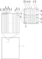
The configuration of the imaging element 7 will be described with reference to fig. 5.
The imaging element 7 is formed by arranging pixels in a matrix in the row direction and the column direction. Each pixel 21 is one of a light-shielded pixel 21A provided with a light-shielding portion that shields a part of light incident on one pixel and a PD-divided pixel 21B configured by two divided pixels.
The imaging element 7 includes a first pixel row 22A including the light-shielding pixels 21A to output a phase difference signal of the PD light-shielding method and a second pixel row 22B including only the PD-divided pixels 21B to output a phase difference signal of the PD division method.
The first pixel rows 22A are discretely provided in the vertical direction, and a plurality of rows of the second pixel rows 22B are arranged between the first pixel rows 22A and the first pixel rows 22A. The first pixel rows 22A may be regularly arranged or may be irregularly arranged. However, when the imaging elements 7 are regularly arranged, the design cost and the manufacturing cost associated with the manufacturing of the imaging elements 7 can be suppressed.
Each of the PD split pixels 21B included in the second pixel row 22B is covered with a color filter of a Bayer (Bayer) array, and is one of a PD split pixel having a spectral sensitivity of red (R), a PD split pixel having a spectral sensitivity of green (G), and a PD split pixel having a spectral sensitivity of blue (B) according to the type of the color filter.
The configuration of the light-shielded pixel 21A will be described with reference to the schematic diagram of fig. 6.
The light-shielding pixel 21A includes a PD 30, a light-shielding section 31 arranged in front of the PD 30 (on the object side), an inner lens 32 arranged in front of the light-shielding section 31, a color filter (cyan) 33 arranged in front of the inner lens 32, and an on-chip microlens 34 arranged in front of the color filter 33.
Note that the inner lens 32 and the color filter 33 may not be provided in the light-shielded pixel 21A.
The PD 30 is a light receiving element on which a part of light passing through the exit pupil EP is incident, but light can be received only in a partial area in the light receiving area of the PD 30 by the light shielding portion 31 arranged in the front.
That is, the light shielding portion 31 is formed to cover the left half region of the PD 30. The right opening 35R is formed in the light shielding section 31.
The inner lens 32 and the on-chip microlens 34 are optical components provided for efficiently condensing light passing through the exit pupil EP and entering one pixel on the PD 30.
The color filter 33 is, for example, an optical filter having a cyan (Cy) spectral sensitivity.
As shown in fig. 6, the PD 30 is configured to receive only light passing through a left region (hereinafter, described as "left pupil region EPL"), which is a left half region of the exit pupil EP. That is, light passing through a right region (hereinafter, described as "right pupil region EPR") which is a right half region of the exit pupil EP is shielded by the light shielding portion 31 and does not reach the PD 30. Thus, a pupil division function is realized.
The light-shielded pixels 21A configured to receive light passing through the left pupil area EPL as shown in fig. 6 are referred to as light-shielded pixels 21AR because light is received in an area deviated to the right on the light receiving surface. That is, in the light-shielded pixel 21AR, the right opening 35R is formed.
Further, the light-shielded pixel 21A having a mirror-symmetric configuration with respect to the configuration shown in fig. 6 is a light-shielded pixel 21A configured to receive light passing through the right pupil region EPR, and this pixel receives light in a region deviated to the left side on the light receiving surface, and is therefore referred to as a light-shielded pixel 21 AL. The left opening 35L is formed in the light shielding section 31 included in the light shielding pixel 21 AL.
As shown in fig. 5, the distance between the light-shielded pixels 21AR and the light-shielded pixels 21AL is, for example, a distance corresponding to two pixels, and is alternately arranged.
The signal output from the light-shielded pixel 21AR and the signal output from the light-shielded pixel 21AL are processed as a pair of phase difference signals by the camera signal processing unit 8 (or the camera control unit 14). That is, the defocus amount calculating unit 8a of the camera signal processing unit 8 in the subsequent stage calculates the defocus amount using the phase difference between the signal output from the light-shielded pixel 21AR and the signal output from the light-shielded pixel 21 AL.
Next, the PD split pixels 21B will be described.
Fig. 7 is a diagram schematically showing the configuration of a PD split pixel 21B as a pixel 21 in the imaging element 7.
The PD split pixel 21B includes two split pixels, i.e., a left PD 40L as a left split pixel and a right PD 40R as a right split pixel, a pixel boundary metal 41 arranged in front of the split pixels, an inner lens 32, a color filter 33, and an on-chip microlens 34. The color filter 33 is any one of a color filter 33R having a spectral sensitivity of red (R), a color filter 33G having a spectral sensitivity of green (G), and a color filter 33B having a spectral sensitivity of blue (B).
Note that the inner lens 32 and the like may not be provided in the PD split pixel 21B.
As shown, the left PD 40L receives light that has passed through the right pupil area EPR of the exit pupil EP. The right PD 40R receives light that has passed through the left pupil area EPL. Thus, a pupil division function is realized.
<3.AF control >
An AF control method for performing focusing using each pixel 21 described above will be described.
First, AF control using a phase difference signal output from the light-shielded pixel 21A or the PD split pixel 21B will be described.
The phase difference signal will be described using the light-shielded pixels 21A as an example.
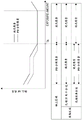
Fig. 8 is a graph showing a relationship between the position and the output of the light-shielded pixel 21A for the specific first pixel row 22A on the imaging element 7.
The signal output from the light-shielded pixel 21AL in which the left opening 35L is formed is indicated by a solid line. Further, a signal output from the light-shielded pixel 21AR in which the right opening 35R is formed is indicated by a broken line. The solid line graph is defined as the left open pixel output 50L and the dashed line graph is defined as the right open pixel output 50R.
The shaded portion in fig. 9 represents the difference integral value between the waveform of the left opening pixel output 50L and the waveform of the right opening pixel output 50R.
Next, a waveform obtained by shifting the waveform of the left opening pixel output 50L by a certain distance in the right direction of the graph is illustrated as a waveform 50L1 in fig. 10. The shaded portion in fig. 10 represents the difference integral value between the waveform 50L1 and the right opening pixel output 50R.
A waveform obtained by shifting the waveform 50L1 by a certain distance further to the right direction is illustrated as a waveform 50L2 in fig. 11. The shaded portion in fig. 11 represents the difference integral value between the waveform 50L2 and the right opening pixel output 50R.
A waveform obtained by further shifting the waveform 50L2 by a distance in the right direction is illustrated as a waveform 50L3 in fig. 12. The shaded portion in fig. 12 represents the differential integrated value between waveform 50L3 and right open pixel output 50R.
A graph of the differential integrated values shown in the shaded portions of fig. 9, 10, 11 and 12 is shown in fig. 13.
As shown in the figure, the differential integral value decreases as the shift amount increases, and when a predetermined shift amount is exceeded, the differential integral value increases again as the shift amount increases.
The shift amount with the smallest difference integrated value is the phase difference. That is, by moving the focus lens so that the outputs of the light-shielded pixels 21AL and 21AR are phase-difference shifted and the waveforms of the left open pixel output 50L and the right open pixel output 50R substantially overlap, appropriate AF control can be performed.
Note that a so-called front pin (front pin) and rear pin (rear pin) can be distinguished according to the direction of the waveform shift of the left aperture pixel output 50L. That is, in the state of fig. 9, by shifting the waveform of the left aperture pixel output 50L to the right, the differential integration value can be minimized. This state is the so-called front pin state.
On the other hand, in a case where the differential integrated value can be made the minimum value by shifting the waveform of the left-opening pixel output 50L in the left direction, a so-called rear pin state is set.
Note that, in detail, since the light-shielded pixels 21AL and the light-shielded pixels 21AR are separated by two pixels on the imaging element 7, the best focus state can be created by shifting the focus lens so that the waveforms of the left open pixel output 50L and the right open pixel output 50R are shifted by two pixels.
Fig. 14 shows the relationship between the shift amount and the defocus amount. The shift amount is a shift amount in which the differential integral value shown in fig. 13 is initially decreased, and can be described anew as a phase difference. The relationship between the shift amount and the defocus amount is represented by a linear function. The larger the shift amount, the larger the defocus amount, and the state where the shift amount is large, that is, the state where focusing is not achieved. The defocus amount can be calculated from the shift amount.
Although the AF control based on the phase difference signal output from the light-shielded pixel 21A has been described so far, the AF control based on the phase difference signal output from the PD divided pixel 21B may be similarly performed.
Specifically, the defocus amount can be obtained by comparing the waveform of the signal output from the left PD 40L of the PD divided pixel 21B (corresponding to the left opening pixel output 50L in each drawing) with the waveform of the signal output from the right PD 40R (corresponding to the right opening pixel output 50R in each drawing), and calculating the shift amount for substantially matching these waveforms.
Note that in the case where the defocus amount with high reliability cannot be calculated from the signal output from the light-shielded pixel 21A or the PD split pixel 21B, it is conceivable to calculate the defocus amount using a contrast method.
For example, contrast is detected based on a luminance signal generated in the camera signal processing unit 8, and focus control is performed.
Note that the contrast method described here is an example, and the defocus amount can be calculated by the contrast method using various known methods.
<4. on-axis region and off-axis region >
In the imaging element 7, the arrangement of the pixels 21 may be different between the region near the center and the other regions. Specifically, a region near the center of the imaging element 7 is described as an on-axis region ArC, and the other regions are described as off-axis regions ArM.
Note that fig. 15 shows an example of the on-axis region ArC and the off-axis region ArM, but the on-axis region ArC may be a substantially circular region or may have other shapes. Further, whether each pixel belongs to the on-axis region ArC or the off-axis region ArM is stored in advance in the memory unit 15. Therefore, the camera control unit 14 can determine whether the pixel or region belongs to the on-axis region ArC or the off-axis region ArM with reference to the storage unit 15.
As shown in fig. 16, the pixels 21C arranged in the on-axis region ArC receive light incident from a direction substantially perpendicular to the light receiving surface. On the other hand, the pixels 21M arranged in the off-axis region ArM receive light incident on the light receiving surface from an oblique direction as shown in the drawing.
Each pixel 21 of the imaging element 7 is configured such that each portion is shifted toward the central portion side as it is positioned at a distance farther from the central portion.
The light-shielded pixel 21AR shown in fig. 6 is an example of the pixel 21C arranged substantially at the center of the on-axis region ArC, for example.
The shading pixel 21AR as the pixel 21M disposed in the off-axis region ArM will be described with reference to fig. 17.
As shown in the figure, the inner lens 32 and the color filter 33 are disposed to be shifted toward the exit pupil EP side with respect to the PD 30 and the light shielding portion 31. Further, the on-chip microlens 34 is disposed to be shifted toward the exit pupil EP side with respect to the inner lens 32 and the color filter 33.
With this configuration, light obliquely incident from the exit pupil EP can be efficiently incident on the PD 30.
Next, a PD split pixel 21B as a pixel 21M arranged in the off-axis region ArM is shown in fig. 18.
As shown in the drawing, the pixel boundary metal 41 is arranged in front of the left PD 40L and the right PD 40R, and the inner lens 32 and the color filter 33 are arranged in front of the pixel boundary metal 41 so as to be shifted toward the exit pupil EP side with respect to the pixel boundary metal 41. Further, the on-chip microlens 34 is disposed so as to be shifted toward the exit pupil EP side with respect to the inner lens 32 and the color filter 33.
The shift amount of each unit such as the inner lens 32 and the color filter 33 is determined according to the arrangement position of the pixel 21 regardless of whether the pixel 21 is the light-shielded pixel 21A or the PD-divided pixel 21B. Therefore, it becomes easy to form each portion on the imaging element 7.
Further, since each portion is shifted, light obliquely incident from the exit pupil EP can be effectively incident on the left PD 40L and the right PD 40R, and light passing through the left pupil area EPL is incident on the right PD 40R, and light passing through the right pupil area EPR is incident on the left PD 40L. That is, the pupil division function is realized.
<5. pupil distance and pixel Structure >
The angle of light incident on the pixel 21 is also affected by the distance between the exit pupil and the imaging element 7. The shorter the distance between the exit pupil and the imaging element 7, the larger the angle of incidence on the pixel 21. When the incident angle changes, the light receiving area of the PD 30 that receives light that has passed through the left pupil area EPL changes.
For example, fig. 17 shows a configuration in a case where the pupil distance of the exit pupil EP is a predetermined distance and the right opening 35R is larger than half of the surface area of the PD 30.
In the case where the lens barrel 3 is an interchangeable lens, the pupil distance of the exit pupil EP changes depending on the type of the optical system 16. In the case where the exit pupil EP is closer than the predetermined distance, the light-shielded pixel 21AR shown in fig. 17 receives not only light passing through the left pupil area EPL of the exit pupil EP but also light passing through the right pupil area EPR.
Therefore, in the present embodiment, a plurality of types of light-shielded pixels 21AR and light-shielded pixels 21AL according to the pupil distance of the exit pupil EP are provided.
This will be described in detail with reference to fig. 17 and 19. In fig. 17, for the optical system 16 in which the pupil distance of the exit pupil EP is set to a predetermined distance, the right opening 35R of the light shielding section 31 is formed so that the light passing through the left pupil area EPL is received by the PD 30.
On the other hand, in fig. 19, for the optical system 16 in which the pupil distance of the exit pupil EP is shorter than the predetermined distance, the right opening 35R of the light shielding section 31 is formed so that the light passing through the left pupil area EPL is received by the PD 30.
As understood from these two drawings, in order for the PD 30 to receive light that has passed through the left pupil area EPL in the optical system 16 having a short pupil distance, it is necessary to process incident light that is incident more obliquely.
That is, in the structure shown in fig. 19, the right opening 35R is narrowed, and the opening end of the right opening 35R on the exit pupil EP side is at a position further away from the exit pupil EP.
By adopting such a configuration, the light-shielded pixels 21AR and 21AL can be made to correspond to a case where the pupil distance of the exit pupil EP is short, and the pupil division function can be made to function.
Note that in the light-shielded pixel 21AR shown in fig. 17 and 19, the amounts of shift of the inner lens 32, the color filter 33, and the on-chip microlens 34 are the same.
That is, only the right opening 35R of the light shielding section 31 is different in shape.
A plurality of light-shielded pixels 21AR and 21AL shown in fig. 17 and a plurality of light-shielded pixels 21AR and 21AL shown in fig. 19 are provided on the imaging element 7.
In the present example, eight kinds of light-shielded pixels 21AR and light-shielded pixels 21AL corresponding to pupil distances are arranged on the imaging element 7. That is, in the eight kinds of light-shielded pixels 21AR and 21AL, the opening areas of the right opening 35R and the left opening 35L are different in eight stages.
In the following description, eight kinds of pupil distances are referred to as pupil distance S0 to pupil distance S7 in order from the closest pupil distance.
Then, the light-shielded pixels 21AR and 21AL corresponding to the pupil distance S0 are set as light-shielded pixels RS0 and LS 0. Similarly, the light-shielded pixel 21AR and the light-shielded pixel 21AL corresponding to the pupil distance S1 are set as light-shielded pixels RS1 and LS1, the light-shielded pixel 21AR and the light-shielded pixel 21AL corresponding to the pupil distance S2 are set as light-shielded pixels RS2 and LS2, the light-shielded pixel 21AR and the light-shielded pixel 21AL corresponding to the pupil distance S3 are set as light-shielded pixels RS3 and LS3, the light-shielded pixel 21AR and the light-shielded pixel 21AL corresponding to the pupil distance S4 are set as light-shielded pixels RS4 and LS4, the light-shielded pixel 21AR and the light-shielded pixel 21AL corresponding to the pupil distance S5 are set as light-shielded pixels RS5 and LS5, the light-shielded pixel 21AR and the light-shielded pixel 21AL corresponding to the pupil distance S6 are set as light-shielded pixels RS6 and LS6, the light-shielded pixel 21AR and the light-shielded pixel 21AL corresponding to the pupil distance S7 are set as light-shielded pixels RS7 and LS 7.
Further, the first pixel row in which the light-shielded pixels RS0 and LS0 are disposed is set as a first pixel row 22a0, the first pixel row in which the light-shielded pixels RS1 and LS1 are disposed is set as a first pixel row 22a1, the first pixel row in which the light-shielded pixels RS2 and LS2 are disposed is set as a first pixel row 22a2, the first pixel row in which the light-shielded pixels RS3 and LS3 are disposed is set as a first pixel row 22A3, the first pixel row in which the light-shielded pixels RS4 and LS4 are disposed is set as a first pixel row 22A4, the first pixel row in which the light-shielded pixels RS5 and LS5 are disposed is set as a first pixel row 22A5, the first pixel row in which the light-shielded pixels RS6 and LS6 are disposed is set as a first pixel row 22a 582, and the first pixel row in which the light-shielded pixels RS7 and LS 68653 are disposed is set as a first pixel row 7a first pixel row 22a 7.
Fig. 20 shows an example of arrangement patterns of the first pixel rows 22a0 to 22a 7.
Fig. 20 is an enlarged view of a part of the imaging element 7. As shown in the figure, the first pixel row 22a0 in which the light-shielded pixels RS0 and LS0 are disposed and the first pixel row 22a7 in which the light-shielded pixels RS7 and LS7 are disposed to be vertically separated from each other by a certain distance, and the pixel rows of the first pixel row 22a0 to the first pixel row 22a7 are periodically disposed in the vertical direction.
Each of the first pixel row 22a0 to the first pixel row 22a7 outputs a phase difference signal SG0 to a phase difference signal SG7 to calculate a defocus amount, and the defocus amount calculating unit 8a in the subsequent stage selects an appropriate phase difference signal SG according to the pupil distance of the exit pupil EP and calculates the defocus amount. For example, in the case where the pupil distance of the exit pupil EP is the pupil distance S3, the defocus amount is calculated using the phase difference signal SG3 output from the first pixel row 22 A3.
Next, the relationship of the PD divided pixels 21B, which are the pixels 21M arranged in the off-axis region ArM, with the pupil distance will be described. In the PD divided pixel 21B arranged in the off-axis region ArM, the condition that only light that has passed through the left pupil region EPL is incident on the right PD 40R and only light that has passed through the right pupil region EPR is incident on the left PD 40L is only the case of using the optical system 16 having the pupil distance designed in the imaging element 7. In this case, since light passing through the center of the exit pupil EP enters the boundary between the two divided pixels, the pupil division function works appropriately.
However, in the case of using the optical system 16 having a pupil distance different from the pupil distance designed by the imaging element 7, light passing through the center of the exit pupil EP is unevenly incident on any one of the divided pixels. In order to make the pupil division function appropriately in this state, it is conceivable to change the ratio of the sizes of the two divided pixels so that light passing through the center of the exit pupil EP enters the boundary between the two divided pixels. That is, as with the light-shielded pixels 21A of plural types provided on the imaging element 7, it is necessary to provide PD-divided pixels 21B respectively corresponding to the pupil distances S0 to S7 in the imaging element 7.
However, changing the area ratio of the two split pixels of each PD split pixel 21B has great technical difficulty and leads to an increase in manufacturing cost.
Therefore, in the imaging device 1 according to the present embodiment, only the PD-divided pixels 21B corresponding to a certain pupil distance (e.g., pupil distance S3) are set on the imaging element 7.
Note that here, an example has been described in which eight kinds of light-shielded pixels 21AR and light-shielded pixels 21AL are provided according to the pupil distance, but other types may be provided. That is, only one type of the light-shielded pixels 21AR and the light-shielded pixels 21AL may be provided regardless of the pupil distance, or a plurality of types may be provided according to the pupil distance.
<6. difference in AF control due to difference in phase difference pixels >
The AF control performed based on the phase difference signal output from the imaging element 7 has been described to include a method of using the light-shielded pixels 21A and a method of dividing the pixels 21B using the PD.
Here, the difference therebetween will be described with reference to fig. 21.
First, the light-shielded pixel 21A is a pixel dedicated to phase difference detection with respect to the application of each pixel. That is, these pixels are pixels that are not used to generate a normal image signal. The normal image signal is a signal for generating an image of the subject. Since the light-shielded pixel 21A shields a part of light incident on the pixel region through the light-shielding section 31, the output signal of the light-shielded pixel 21A is not used for generating a normal image signal.
On the other hand, the PD split pixels 21B are pixels used for phase difference detection and also used for generating normal image signals. By adding the outputs of the left PD 40L and the right PD 40R, the PD split pixel 21B can be regarded as a normal pixel.
As for the number of arrangements, as shown in fig. 5, the number of light-shielded pixels 21A decreases, and the number of PD-divided pixels 21B increases.
Since the light-shielded pixels 21A cannot be used as ordinary pixels (i.e., pixels for generating an image of a subject), a large number of light-shielded pixels cannot be provided. Further, since a large number of light-shielded pixels cannot be provided, a large number of light-shielded pixels having the same light-shielding area cannot be included, and output signals cannot be added. Therefore, in the case where AF control is performed using the light-shielded pixels 21A, low illuminance performance is degraded.
On the other hand, since the PD divided pixels 21B can be used as normal pixels, a large number of PD divided pixels can be set, and since the left PD 40L and the right PD 40R have the same size, a plurality of output signals can be added. Therefore, the S/N ratio can be improved and the low illuminance performance is high.
Pupil correction design flexibility will be described.
In the light-shielded pixel 21A, it is relatively easy to separately create the light-shielding sections 31 having different light-shielding areas. Therefore, since it is easy to set a plurality of types of light-shielded pixels 21A (light-shielded pixels RS0 to RS7 and LS0 to LS7) according to a plurality of pupil distances, the phase difference signal can be output with high reliability even if the pupil distances are different. Therefore, the light-shielded pixel 21A has pupil correction design flexibility.
On the other hand, since it is difficult to manufacture the PD divided pixels 21B by changing the ratio of the sizes of the left PD 40L and the right PD 40R, it is difficult to provide a plurality of types of PD divided pixels 21B according to a plurality of pupil distances. Therefore, in the present embodiment, only the PD divided pixels 21B corresponding to a certain pupil distance are provided on the imaging element 7. Therefore, if the pupil distance is different from the design, the reliability of the phase difference signal is reduced. That is, the PD divided pixels 21B do not have pupil correction design flexibility.
Off-axis performance corresponds to pupil correction design flexibility. The off-axis performance is the accuracy of AF control on the subject exposed in an off-axis region ArM, which is a region other than an on-axis region ArC, which is a rectangular region arranged near the center of the imaging element 7.
Since the light-shielded pixel 21A has pupil correction design flexibility, even if light passing through the exit pupil EP is obliquely incident on the light-shielded pixel 21A located in the off-axis region ArM, an appropriate phase difference signal is output in any of the light-shielded pixels RS0 to RS7 and the light-shielded pixels LS0 to LS 7. Therefore, the off-axis performance of the shielded pixel 21A is high.
On the other hand, since the PD-divided pixels 21B do not have pupil correction design flexibility, in the case where the pupil distance is different from the design, when the light passing through the exit pupil EP is obliquely incident on the PD-divided pixels 21B located in the off-axis region ArM, the pupil division function does not function well, and the reliability of outputting the phase difference signal is lowered. Therefore, the off-axis performance when the PD split pixel 21B is used is lower than that when the shading pixel 21A is used.
<7. selection of phase difference signal >
In the present embodiment, which phase difference signal is selected from the phase difference signals output from the light-shielded pixels 21A and the PD divided pixels 21B when calculating the defocus amount will be described with reference to fig. 22.
The upper graph of fig. 22 illustrates the change in AF error in the on-axis region ArC with respect to the exposure amount. The solid line in the figure indicates a case where AF control based on the phase difference signal output from the light-shielded pixel 21A is performed. Further, the broken line in the figure indicates a case where AF control based on the phase difference signal output from the PD divided pixel 21B is performed.
The lower part of the graph of fig. 22 shows the phase difference signal selected for each combination of the exposure amount and the AF control target region.
First, it is conceivable to select a phase difference signal output from one of the light-shielded pixels 21A and the PD divided pixels 21B in accordance with the exposure amount. For example, in the case where the exposure amount is equal to or larger than the threshold Th, the phase difference signal output from the light-shielded pixel 21A is selected. This is because the phase difference signal output from the light-shielded pixel 21A has a short reading time (specifically, described later), and if there is no problem in the calculation of the defocus amount, it is desirable to select the phase difference signal output from the light-shielded pixel 21A.
On the other hand, in the case where the exposure amount is smaller than the threshold Th, if the phase difference signal output from the light-shielded pixel 21A is selected, the reliability of the calculated defocus amount is lowered. Therefore, it is conceivable to select the phase difference signal output from the PD divided pixel 21B. Note that in this example, in the case where the exposure amount is smaller than the threshold Th, one of the phase difference signals output from the light-shielded pixels 21A and the PD divided pixels 21B or the contrast method is selected in consideration of other conditions.
A detailed description will be given.
In the case where the exposure amount is equal to or larger than the threshold Th, the phase difference signal output from the light-shielded pixel 21A is selected regardless of whether the region is the on-axis region ArC or the off-axis region ArM. Reading of charges obtained by photoelectrically converting light received by the light-shielded pixels 21A and the PD split pixels 21B in the case where the exposure amount is equal to or larger than the threshold Th will be described with reference to fig. 23 and 24.
The signal output from the light-shielded pixel 21A is read out as a phase difference signal SGn for each pixel row. The phase difference signal SGn is one of phase difference signals SG0 to SG7, and an appropriate phase difference signal SGn is selected according to the pupil distance.
Since the signal output from the PD divided pixel 21B is used to generate a normal image signal, a signal obtained by adding the outputs of the divided pixels is read. Fig. 24 shows the read timing of signals from the light-shielded pixels 21A and the PD split pixels 21B.
As shown in the figure, the readout of the first pixel row 22A to which the light-shielded pixel 21A that acquires the phase difference signal SGn among the light-shielded pixels 21A belongs is performed sequentially from the upper side of the imaging element 7 in accordance with the vertical synchronization signal Vsync. The readout time required to read out all the phase difference signals SGn output from the imaging elements 7 is set to time T1.
The signal output from the PD split pixel 21B includes a signal SGR output from the PD split pixel 21Br and the second pixel row 22B to which the PD split pixel 21Bg belongs, and a signal SGB output from the PD split pixel 21Bb and the second pixel row 22B to which the PD split pixel 21Bg belongs. The signal SGR and the signal SGB are read sequentially from the top of the imaging element 7.
The readout time required to read out all the signals SGR and SGB output from the imaging element 7 is set to time T2.
Since the number of PD split pixels 21B is larger than the number of light-shielded pixels 21A, the time T2 is set longer than the time T1.
In the case where the exposure amount is equal to or larger than the threshold Th, the fast AF control can be realized by using the phase difference signal from the light-shielded pixel 21A having a short readout time. Further, in the off-axis region ArM, the reliability of the phase difference signal output from the PD split pixel 21B decreases as the pupil distance is farther from the design distance, but in the case where the exposure amount is equal to or larger than the threshold Th, this can be avoided by selecting the phase difference signal output from the light-shielded pixel 21A in the off-axis region ArM.
Further, since the signal readout time is short in the light-shielded pixels 21A, the time until completion of focusing by AF control can be shortened.
Next, a case where the exposure amount is smaller than the threshold Th will be described.
In the on-axis region ArC, the phase difference signal output from the PD divided pixel 21B is selected. Reading of charges obtained by photoelectrically converting light received by the light-shielded pixels 21A and the PD division pixels 21B will be described with reference to fig. 25 and 26.
The output signal from the first pixel row 22A in which the light-shielded pixels 21A are disposed is used to generate a normal image signal. Specifically, only the output signal from each of the split pixels 21Bg that are the PD split pixels 21Bg arranged between the light-shielded pixels 21A is read out.
Since an output signal from the second pixel row 22B in which the PD divided pixels 21B are disposed is used as a phase difference signal, the output of each divided pixel is read out (see fig. 25). Further, since the exposure amount is smaller than the threshold Th, in order to increase the S/N ratio, the required output numbers of the adjacent second pixel rows 22B are added to increase the S/N ratio of the phase difference signal. In fig. 25, two second pixel rows 22B are added, but in the case where the exposure amount is further reduced, three or more second pixel rows 22B are added. Therefore, deterioration of the S/N ratio can be suppressed with respect to a decrease in the exposure amount, and appropriate AF control can be performed.
Note that the phase difference signal from the second pixel row 22B includes the phase difference signal SGr output from the second pixel row 22B including the PD divided pixels 21Br and the phase difference signal SGb output from the second pixel row 22B including the PD divided pixels 21 Bb. In the addition of the phase difference signals, the phase difference signals SGr are added, and the phase difference signal SGb is added.
Fig. 26 shows the read timing of the signal from the PD split pixel 21B. Note that the signal from the light-shielded pixel 21A is not used for AF control or image signal generation, and is therefore not read.
The phase difference signals SGr and SGb output from the PD divided pixels 21B are sequentially read out from the top of the imaging element 7.
The readout time required to read out all the phase difference signals SGr, SGb output from the imaging element 7 is set to time T3. Time T3 is substantially twice time T2 in fig. 24. As shown in fig. 23 and 25, this is based on the difference whether reading is performed in units of pixels or in units of divided pixels.
Next, the phase difference signal in the case where the exposure amount is smaller than the threshold Th and is in the off-axis region ArM will be described. In this case, as shown in fig. 22, the phase difference signal output from the light-shielded pixel 21A is selected.
In this case, as shown in fig. 23 and 24, the phase difference signal SGn output from the first pixel row 22A is read at time T1, and the signals SGR and SGB for generating normal image signals output from the second pixel row 22B are read out at time T2.
However, in the case where the optical system 16 includes an ideal pupil distance set for the PD divided pixels 21B, the phase difference signal output from the PD divided pixels 21B can be selected even in the AF control of the off-axis region ArM. In this case, as shown in fig. 25 and 26, the phase difference signal SGn output from the light-shielded pixels 21A of the first pixel row 22A is not read, but the outputs from the PD divided pixels 21B arranged in the first pixel row 22A and the second pixel row 22B are read at time T3.
Note that in the off-axis region ArM in the case where the optical system 16 includes an ideal pupil distance set for the PD divided pixel 21B, it may not be clear which of the phase difference signal output from the light-shielded pixel 21A and the phase difference signal output from the PD divided pixel 21B has high reliability. In this case, both the phase difference signal of the light-shielded pixel 21A and the phase difference signal of the PD divided pixel 21B are acquired, and the AF control can be performed using both of them.
Fig. 27 and 28 show a case where the phase difference signal from the light-shielded pixel 21A and the phase difference signal from the PD divided pixel 21B are acquired.
As shown in fig. 27, the phase difference signal SGn output from the first pixel row 22A in which the light-shielded pixels 21A are arranged and the phase difference signals SGr and SGb output from the second pixel row 22B in which the PD-divided pixels 21B are arranged are read out.
The reading time of the phase difference signal SGn is set to time T1, and the reading time of the phase difference signal SGr and the phase difference signal SGb is set to time T3. The total readout time obtained by adding the time T1 to the time T3 is shorter than one cycle of the vertical synchronization signal Vsync.
Note that in fig. 22, it has been described that the phase difference signal output from the light-shielded pixel 21A is used in the off-axis region ArM where the exposure amount is smaller than the threshold Th. However, there is a case where sufficient AF control cannot be performed even with the use of the phase difference signal output from the light-shielded pixel 21A. For example, there are cases where the exposure amount is significantly lower than the threshold Th, and the pupil distance of the exit pupil is significantly different from the design of the PD divided pixel 21B.
In this case, AF control by the above-described contrast method can be performed. Therefore, appropriate AF control can be performed under a wide range of conditions.
<8. control of Exposure >
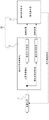
Although it has been described that the phase difference signal is selected based on the exposure amount, here, calculation of the exposure amount will be described with reference to fig. 29.
The imaging element 7 outputs a normal pixel output for generating a normal image signal and a phase difference pixel output as a phase difference signal for AF control.
The normal pixel output and the phase difference pixel output are input to an output level detection circuit included in the camera signal processing unit 8. The output level detection circuit calculates an output average value in the exposure calculation target region on the pixel based on the input normal pixel output and phase difference pixel output, and each output average value is output from the camera signal processing unit 8 and input to the camera control unit 14.
Note that the exposure calculation target region is a region determined according to the photometric mode, and is a region in the image where exposure calculation is to be performed. For example, in the case where the "center-weighted metering mode" is selected, exposure calculation is performed on the center portion of the image. Further, in the case where the "spot light measurement mode" is selected, a specified narrow region is set as a target of exposure calculation. Further, in the case where the "entire-screen averaging photometry mode" is selected, exposure calculation is performed for the area of the entire image.
The camera control unit 14 calculates an exposure amount from the detection result output from the camera signal processing unit 8, and determines a shutter speed (or a parameter such as an F value or a gain that can adjust the exposure amount). The camera control unit 14 performs processing for setting the determined shutter speed to the imaging element 7.
The shutter speed is set, for example, by setting the travel timing of the electronic back film.
The exposure amount calculation performed by the camera control unit 14 may be performed based on only the normal pixel output, or may be performed based on only the phase difference pixel output. Further, exposure control may be performed based on both the normal pixel output and the phase difference pixel output. In this case, exposure control of the phase difference pixel is performed based on the phase difference pixel output, and exposure control of the normal pixel is performed based on the normal pixel output.
<9. Process flow >
<9-1. first example >
A first example of the processing flow of AF control is shown in fig. 30, 31, and 32.
Note that each process shown in fig. 30, 31, and 32 is a process performed by the camera control unit 14 and the camera signal processing unit 8 of the imaging apparatus 1. Here, the camera control unit 14 and the camera signal processing unit 8 are collectively referred to as "processing unit 60".
When the half-pressed state of the shutter button 6S, which is one of the operators 6, is detected, in step S101, the processing unit 60 (the camera control unit 14 or the camera signal processing unit 8) of the imaging apparatus 1 performs exposure amount calculation. In the exposure amount calculation, as described with reference to fig. 29, the detection processing is performed on the output level of one or both of the normal pixel output and the phase difference pixel output, and the exposure amount is calculated based on the detection result.
In step S102, the processing unit 60 determines whether the exposure amount is equal to or greater than the threshold Th.
In the case where the exposure amount is equal to or larger than the threshold Th, the processing unit 60 performs addition readout setting on the PD divided pixels 21B in step S103. The addition readout setting is a setting for adding and simultaneously reading out the charges accumulated in the left PD 40L and the right PD 40R included in the PD split pixel 21B. That is, the PD split pixel 21B is regarded as one pixel.
Next, the processing unit 60 reads out the light-shielded pixel 21A in step S104, and performs addition reading of the PD divided pixel 21B in step S105. Therefore, the phase difference signal read from the light-shielded pixel 21A and the normal pixel signal read from the PD divided pixel 21B are read out.
In step S107, the processing unit 60 calculates a defocus amount based on the phase difference signal output from the light-shielded pixel 21A. At this time, the processing unit 60 calculates the defocus amount using the outputs from the first pixel rows 22a0 to 22a7 including the appropriately shielded pixels 21A according to the pupil distance of the exit pupil EP. Note that, for example, when the lens barrel 3 is mounted to the imaging apparatus 1, the camera control unit 14 acquires a pupil distance of the exit pupil EP from the barrel control unit 18, and stores the pupil distance in the storage unit 15.
In step S108, the processing unit 60 generates display image data of a through image based on the pixel signals from the PD split pixels 21B. The display image data generated here is displayed as a through image on the EVF monitor 5a, the rear monitor 4, or the like.
The processing unit 60 performs lens driving based on the defocus amount in step S109 of fig. 31, and stops the lens driving in step S110. As a result, the focus lens arranged within the lens barrel 3 is driven and focused via the driver unit 17.
In step S111, the processing unit 60 determines whether the half-pressed state of the shutter button 6S is being detected. In a case where the half-pressed state of the shutter button 6S continues, the processing unit 60 returns to the processing of step S101 in fig. 30, and performs focus control according to the exposure amount.
Therefore, as long as the half-pressed state of the shutter button 6S continues, the in-focus state is continuously maintained.
In the case where it is determined in step S102 that the exposure amount is smaller than the threshold Th, the processing unit 60 performs non-addition readout setting on the PD divided pixels 21B in step S112. The non-addition readout setting is a setting for readout so that the electric charges accumulated in each of the left PD 40L and the right PD 40R included in the PD divided pixel 21B at a time can be distinguished. That is, each divided pixel is independently processed.
The processing unit 60 reads out the light-shielded pixel 21A in step S113, and performs non-addition readout of the PD-divided pixels in step S114.
In step S115, the processing unit 60 calculates a defocus amount based on the phase difference signal output from the light-shielded pixel 21A. Further, in step S116, the processing unit 60 calculates a defocus amount based on the phase difference signal output from the PD divided pixel 21B.
By performing the respective processes from step S113 to step S116, focus control can be performed based on the phase difference signals of the light-shielded pixels 21A and the PD split pixels 21B, respectively.
In step S117 of fig. 32, the processing unit 60 performs addition processing on each PD split pixel 21B so as to combine non-addition signals output from the split pixels of the PD split pixel 21B, and performs processing for generating display image data of a through image.
In step S118, the processing unit 60 compares the difference integral values in calculating the defocus amount of each of the light-shielded pixels 21A and the PD divided pixels 21B. The differential integral value represents the magnitude of the phase difference as described with reference to each of fig. 8 to 12. In the calculation of the defocus amount, the shift amount of the waveform is determined so that the difference integral value decreases, but it can be considered that, when the final defocus amount is calculated, the smaller the difference integral value, the higher the reliability of the calculated defocus amount.
Step S118 is comparison processing for determining which of the defocus amount calculated based on the output of the light-shielded pixel 21A and the defocus amount calculated based on the output of the PD divided pixel 21B is highly reliable.
In step S119, the processing unit 60 determines whether the differential integral value in the light-shielded pixel 21A is small. In the case where it is determined that the difference integral value in the light-shielded pixel 21A is small, that is, in the case where it is determined that the defocus amount calculated based on the output of the light-shielded pixel 21A has higher reliability, in step S120, the processing unit 60 performs lens driving based on the defocus amount calculated from the output of the light-shielded pixel 21A.
On the other hand, in the case where it is determined in step S119 that the difference integral value in the PD split pixel 21B is small, that is, in the case where it is determined that the defocus amount calculated based on the output of the PD split pixel 21B has higher reliability, the processing unit 60 performs lens driving based on the defocus amount calculated based on the output of the PD split pixel 21B in step S121.
After performing the processing of step S120 or step S121, the processing unit 60 stops the lens driving at step S122.
In step S123, the processing unit 60 determines whether the half-pressed state of the shutter button 6S is being detected. In a case where the half-pressed state of the shutter button 6S continues, the processing unit 60 returns to the processing of step S101 in fig. 30, and performs focus control according to the exposure amount.
Therefore, as long as the half-pressed state of the shutter button 6S continues, the in-focus state is continuously maintained.
Note that in each of the processes described in steps S103 to S111 in fig. 30 and 31, as shown in fig. 23 and 24, the light-shielded pixels 21A are regarded as pixels that output phase difference signals for focus control, and the PD-divided pixels 21B are regarded as pixels that output normal pixel signals.
Further, in each of the processes described in steps S112 to S123 in fig. 30 and 31, as shown in fig. 27 and 28, each of the light-shielded pixels 21A and the PD-divided pixels 21B is regarded as a pixel that outputs a phase difference signal, and the PD-divided pixels 21B are also regarded as pixels that output a normal pixel signal.
As shown in fig. 25 and 26, in the case where the exposure amount is set to be smaller than the threshold Th, the PD split pixels 21B are regarded as the pixels that output the phase difference signals and the pixels that output the normal pixel signals without using the light shielded pixels 21A, which can be realized by not performing the processing of steps S113 and S115 in fig. 30 and the processing of steps S118, S119, and S120 in fig. 32.
<9-2. second example >
A second example of the processing flow of AF control will be described with reference to fig. 30, 31, and 33. Note that processes similar to those in the first example are denoted by the same reference numerals, and description thereof will be omitted as appropriate.
When the half-pressed state of the shutter button 6S is detected, the processing unit 60 (the camera control unit 14 or the camera signal processing unit 8) of the imaging apparatus 1 performs exposure amount calculation in step S101 of fig. 30.
Next, in step S102, the processing unit 60 determines whether the exposure amount is equal to or greater than the threshold Th.
In the case where the exposure amount is equal to or larger than the threshold Th, AF control is performed using the phase difference signal output from the light-shielded pixel 21A. The processing in this case is similar to the processing from step S103 in fig. 30 to step S111 in fig. 31 in the first example.
On the other hand, in the case where it is determined that the exposure amount is smaller than the threshold Th, the processing unit 60 executes each process from step S112 to step S116 in fig. 30, and then executes step S117 in fig. 33.
Thus, the phase difference signal from the light-shielded pixel 21A and the phase difference signal from the PD-divided pixel 21B are acquired, and display image data for through image display is generated based on the signals from the PD-divided pixel 21B.
Next, in step S131 of fig. 33, the processing unit 60 determines whether or not a deviation between the pupil distance of the exit pupil EP of the PD divided pixel 21B outputting an appropriate phase difference signal and the pupil distance of the exit pupil EP of the optical system 16 is a predetermined value or more, that is, whether or not the pupil distance of the exit pupil EP of the optical system 16 is closer, farther, or coincides with the information of the pupil distance of the exit pupil EP acquired from the lens barrel 3.
As described above, since the incident angle of light on the pixel 21 varies depending on the pupil distance of the exit pupil EP, if the pupil distance deviates from the design, it is likely that a phase difference signal with high reliability cannot be acquired from the PD-divided pixels 21B.
In a case where it is determined that the deviation is equal to or larger than the predetermined value, that is, in a case where it is determined that the pupil distance of the exit pupil EP is the optical system 16 closer than the design, or when it is determined that the pupil distance is the optical system 16 farther than the design, the phase difference signal output from the PD divided pixel 21B arranged in the off-axis region ArM has low reliability. Therefore, in step S132, the processing unit 60 calculates the defocus amount using the phase difference signal output from the PD split pixel 21B in the on-axis region ArC and the phase difference signal output from the shading pixel 21A in the off-axis region ArM.
Subsequently, in step S133, the processing unit 60 performs lens driving based on the calculated defocus amount.
On the other hand, in the case where it is determined in step S131 that the deviation of the pupil distance is smaller than the predetermined value, that is, in the case where it is determined that the pupil distance of the exit pupil EP is the designed optical system 16 or in the case where it is determined that the exit pupil EP is the optical system 16 which is closely designed, since the reliability of the phase difference signal output from the PD divided pixels 21B arranged in the off-axis region ArM is high, the processing unit 60 calculates the defocus amount using the phase difference signal output from the PD divided pixels in step S134.
Next, in step S135, the processing unit 60 performs lens driving based on the defocus amount.
After performing the processing of step S133 or step S135, the processing unit 60 stops the lens driving in step S136.
In step S137, the processing unit 60 determines whether the half-pressed state of the shutter button 6S is being detected. In a case where the half-pressed state of the shutter button 6S continues, the processing unit 60 returns to the processing of step S101 in fig. 30, and performs focus control according to the exposure amount.
Therefore, as long as the half-pressed state of the shutter button 6S continues, the in-focus state is continuously maintained.
In the above example, focusing is performed on both the on-axis region ArC and the off-axis region ArM (i.e., the entire surface of the pixel element 7). In addition, there is a case where a predetermined region is focused. For example, in the case where the on-axis area ArC receives reflected light from the person to be focused (i.e., in the case where the person to be focused is captured in the on-axis area ArC), focusing only needs to be performed on the on-axis area ArC (or, particularly, an area in which the person to be focused is captured).
In this case, without performing the determination processing in step S131, the phase difference signal output from the PD-divided pixels 21B in the on-axis region ArC is used to calculate the defocus amount in step S132.
Alternatively, where a person to be focused is shown in the off-axis region ArM, focusing need only be performed on the off-axis region ArM. Specifically, in the case where it is determined to be "yes" in step S131, the phase difference signal output from the light-shielded pixels 21A of the off-axis region ArM is used to calculate the defocus amount (step S132), and in the case where it is determined to be "no" in step S131, the phase difference signal output from the PD split pixels 21B of the off-axis region ArM is used to calculate the defocus amount (step S134).
Further, there may be a case where a person to be focused may appear on the on-axis region ArC and the off-axis region ArM. In this case, as described above, the defocus amount can be calculated by performing the respective processes of steps S131 to S135.
Alternatively, in the case where a person or an object to be focused is not determined, for example, in the case where an instruction from the user is not given, after the defocus amount is calculated for each on-axis region ArC or off-axis region ArM or for each subject (for each region where one subject is photographed) (steps S132 and S134), determination processing for determining a focus target, processing for causing the user to select a focus target or a region of interest (ROI), and the like may be performed before lens driving is performed in steps S133 and S135, and lens driving may be performed according to the determination processing or the result of the selection processing.
<10. modified example >
In the above example, AF control is performed based on the calculated defocus amount. As another example, it is conceivable to perform notification control or display control on the user based on the defocus amount, and manually perform the focusing operation.
For example, the UI control unit 14a of the camera control unit 14 may assist the manual focusing operation of the user by displaying information on focusing on the EVF monitor 5a or the rear monitor 4.
Further, an example has been described in which the above-described light-shielded pixel 21A includes one PD, but a plurality of PDs may be included as divided pixels. For example, all the pixels of the imaging element 7 may be PD divided pixels including two divided pixels. That is, each pixel may include a left PD 40L and a right PF 40R. Even with this configuration, in the light-shielded pixel 21A, by adding and reading outputs from two divided pixels, they can be handled as one PD.
Since all the pixels on the imaging element 7 have the same configuration, the manufacturing of the imaging element 7 can be facilitated. In addition, the manufacturing cost can be reduced.
<11. summary >
As described in each of the above-described examples, the imaging device 1 according to the present technology includes the imaging element 7 including the light-shielded pixel 21A having a pupil division function by including the light-shielding portion 31 that shields one light beam of a pair of light beams that have passed through a pair of partial regions (the left pupil region EPL and the right pupil region EPR) that are deviated in opposite directions in a predetermined direction (for example, the left-right direction) in the exit pupil EP, and the light-receiving element (PD 30) that receives the other light beam; and a photodiode divided pixel (PD divided pixel 21B) having a pupil division function by including divided pixels (left PD 40L and right PD 40R) that respectively receive the pair of light beams passing through the pair of partial regions.
The light-shielded pixel 21A includes, for example, a light-shielded pixel 21AR and a light-shielded pixel 21AL, the light-shielded pixel 21AR being a pixel on which only light passing through a left pupil area EPL is incident, the left pupil area EPL being a left half area of the exit pupil of the light-shielding section 31, the light-shielded pixel 21AL being a pixel on which only light passing through a right pupil area EPR is incident, the right pupil area EPR being a right half area of the exit pupil of the light-shielding section 31.
Further, the PD-divided pixels 21B are so-called PD-divided pixels in which a plurality of divided pixels (left PD 40L and right PD 40R) are arranged in the area of one pixel. Each pixel is, for example, a color pixel of a Bayer (Bayer) array, and includes one color filter 33 and light receiving elements (PD 30, left PD 40L, and right PD 40R) that receive incident light passing through the color filter 33.
Further, the defocus amount calculation unit 8a calculates the defocus amount using at least one of the signal (phase difference signal SG) output from the light-shielded pixel 21A and the signal (phase difference signals SGr and SGb) output from the PD divided pixel 21B based on the exposure amount.
The light-shielded pixel 21A and the PD split pixel 21B each output a phase difference signal capable of calculating a defocus amount. Therefore, in the phase difference signals output from the light-shielded pixels 21A and the PD split pixels 21B, an appropriate defocus amount can be calculated using an appropriate phase difference signal based on the exposure amount.
Further, each pixel included in the imaging element 7 may be one of the light-shielded pixel 21A and the PD divided pixel 21B.
That is, in the imaging element 7, all the pixels are one of the light-shielded pixels 21A and the PD divided pixels 21B.
Therefore, there is no need to complicate the manufacturing of the imaging element 7, and it is possible to shorten the manufacturing time and reduce the manufacturing cost.
As described in the selection of the phase difference signal with reference to fig. 22, the defocus amount calculating unit 8a can calculate the defocus amount using the output signal (phase difference signal SG) of the light-shielded pixel 21A with the exposure amount equal to or larger than the threshold Th.
Since the light-shielded pixel 21A includes the light-shielding section 31, the output signal level is smaller than that of the PD divided pixel 21B.
Further, the number of light-shielded pixels 21A is smaller than the number of PD split pixels 21B, and the light-shielded pixels are discretely provided. Therefore, in the case where the exposure amount is small, the signal level cannot be increased by adding signals output from a plurality of pixels, and it is difficult to improve the S/N ratio. Therefore, there is a possibility that the reliability of the calculated defocus amount is lowered. However, when the exposure amount is equal to or larger than the threshold Th, the output level of the phase difference signal from the light-shielded pixels 21A is equal to or larger than a certain level, so that the reliability of the defocus amount calculated using the output signal of the light-shielded pixels 21A can be improved.
As described in the selection of the phase difference signal with reference to fig. 22, in the case where the exposure amount is smaller than the threshold Th, the defocus amount calculation unit 8a may calculate the defocus amount using at least one of the output signals of the shaded pixels 21A and the output signals of the PD split pixels 21B according to whether it is an on-axis region ArC, which is a region including the central portion of the imaging element 7, or an off-axis region ArM, which is a region of the imaging element 7 other than the on-axis region ArC.
In the case where the exposure amount is smaller than the threshold Th, there are a case where it is preferable to calculate the defocus amount using the output signal of the PD divided pixel 21B having high low-illuminance performance, and a case where it is preferable to calculate the defocus amount using the output signal of the light-shielded pixel 21A capable of selecting an appropriate output according to the pupil distance of the exit pupil EP. According to this configuration, an appropriate output signal of the image plane phase difference pixel can be selected, and the defocus amount can be calculated with high reliability.
As described in the selection of the phase difference signal with reference to fig. 22, the defocus amount calculating unit 8a can calculate the defocus amount using the output signals (phase difference signals SGr and SGb) of the PD divided pixels 21B in the on-axis region ArC.
Since the PD divided pixel 21B does not include the light shielding section 31, the output signal level thereof is higher than that of the light shielding pixel 21A.
Further, the number of PD split pixels 21B is larger than the number of light-shielded pixels 21A. Therefore, even in the case where the exposure amount is low, the S/N ratio of the phase difference signal can be increased by adding the outputs of the plurality of pixel rows, and the output level of the phase difference signal necessary for calculating the defocus amount can be easily secured. Therefore, the in-focus position information and the lens driving amount can be calculated with high accuracy.
As described in the selection of the phase difference signal with reference to fig. 22, the defocus amount calculating unit 8a can calculate the defocus amount using the output signals of the light-shielded pixels 21A in the off-axis region ArM.
Therefore, the defocus amount with high reliability is calculated, and the focusing accuracy can be improved.
As described in the selection of the phase difference signal with reference to fig. 22, the defocus amount calculation unit 8a can calculate the defocus amount using the output signals of the photodiode split pixels (PD split pixels 21B) in the off-axis region ArM.
Therefore, the defocus amount with high reliability is calculated, and the focusing accuracy can be improved.
As described in the selection of the phase difference signal with reference to fig. 22, the defocus amount calculating unit 8a can calculate the defocus amount using the output signal with higher reliability of the output signal of the light-shielded pixel 21A and the output signal of the photodiode-divided pixel (PD-divided pixel 21B).
Therefore, the defocus amount with high reliability is calculated, and the focusing accuracy can be improved.
Each of the split pixels (the left PD 40L and the right PD 40R) of the PD split pixel 21B has, for example, the same light receiving area.
In this case, in order to cause the light passing through the left pupil area EPL of the exit pupil EP to be incident on one divided pixel (the right PD 40R) and the light passing through the right pupil area EPR to be incident on the other divided pixel (the left PD 40L), the optical system 16 needs to include a certain pupil distance according to the arrangement of the on-chip microlenses 34 and the like included in the PD divided pixel 21B. On the other hand, a plurality of types of light-shielded pixels 21A (light-shielded pixels LS0 to LS7 and light-shielded pixels RS0 to RS7) may be provided according to the pupil distance. Therefore, in the off-axis region ArM of the imaging element 7, the light-shielded pixel 21A may have a reduced signal level of the output signal due to an insufficient light reception amount, and the PD-divided pixel 21B may have a reduced reliability of the output signal due to an inappropriate pupil distance. Therefore, if the defocus amount is always calculated based on any one of the phase difference signals, the reliability may be low.
In the above example, in the off-axis region ArM where the exposure amount is smaller than the threshold Th, both the output signal of the shielded pixel 21A and the output signal of the PD split pixel 21B are acquired, and the defocus amount is calculated using the phase difference signal with higher reliability. Therefore, a highly reliable defocus amount can be calculated.
As described in the selection of the phase difference signal with reference to fig. 22, in the case where the exposure amount is less than the threshold Th, the defocus amount calculation unit 8a may perform autofocus control based on the contrast method in the off-axis region ArM, the on-axis region ArC being a region including the center portion of the imaging element 7, the off-axis region ArM being a region other than the on-axis region ArC.
The off-axis region ArM in the case of insufficient exposure amount may have low reliability of phase difference information based on the output signal of the shielded pixel 21A (phase difference signal SG) and the output signal of the PD split pixel 21B (phase difference signals SGr and SGb).
In this case, by adopting the contrast method, appropriate autofocus control can be performed.
As described with reference to fig. 20, in the configuration of the imaging element 7, the imaging element 7 may include a plurality of types of light-shielded pixels 21A (light-shielded pixels LS0 to LS7 and light-shielded pixels RS0 to RS7) according to the pupil distance of the exit pupil EP.
Therefore, even if the pupil position of the exit pupil EP changes when the optical system 16 is driven, an appropriate phase difference signal can be obtained from any one of the plurality of types of light-shielded pixels 21A.
Therefore, for example, even if the pupil distance of the exit pupil EP is made to fluctuate in a wide range by using the interchangeable lens barrel 3 or the like, the defocus amount can be calculated with high reliability.
As described with reference to fig. 17 and 19, in the structure of the imaging element 7, the light-shielding regions of the light-shielding sections 31 that the plurality of types of light-shielding pixels 21A (the light-shielding pixels LS0 to LS7 and the light-shielding pixels RS0 to RS7) have may be different.
For example, the smaller the pupil distance, the larger the light shielding area of the light shielding section 31.
Therefore, in each pixel included in the light-shielded pixel 21A, the light-shielding section 31 is formed so that only light passing through one side region of the exit pupil EP is received according to the pupil distance, and an appropriate output signal (phase difference signal SG) of the light-shielded pixel 21A can be output.
As described with reference to fig. 30 regarding the first example of the processing flow of AF control, the defocus amount calculation unit 8a can calculate the defocus amount using the output signal (phase difference signal SG) of the light-shielded pixel 21A selected according to the pupil distance of the exit pupil EP.
Thus, the light-shielded pixel 21A that receives light passing through one side region of the exit pupil EP is selected.
Therefore, the defocus amount can be calculated with high reliability using an appropriate output signal of the light-shielded pixel 21A.
As described with reference to fig. 30 for the first example of the processing flow of AF control, the camera control unit 14 that acquires the pupil distance from the lens barrel control unit 18 included in the lens barrel 3 may be included.
For example, in the imaging device 1 including the interchangeable lens barrel 3, the light-shielded pixels 21A (a part of the light-shielded pixels LS0 to LS7 and the light-shielded pixels RS0 to RS7) are selected according to the pupil distance.
As described with reference to fig. 20, in the configuration of the imaging element 7, the light-shielded pixels 21A arranged in the same row (the same pixel row) on the imaging element 7 may correspond to the same pupil distance.
Therefore, the output signals of the plural types of light-shielded pixels 21A are not mixed with the pixel signal read for each pixel row.
Therefore, the output signal of the light-shielded pixel 21A selected according to the pupil distance is easily processed, and the processing load can be reduced.
As described with reference to the first and second examples of the processing flow of AF control with reference to fig. 31 and 33, the camera control unit 14 that gives a drive instruction to the focus lens included in the imaging optical system (optical system 16) based on the defocus amount may be included.
Therefore, the focus lens is controlled by the phase difference signal based on the exposure amount.
Therefore, appropriate focus control based on the exposure amount can be performed.
As described in the modified example, a user interface control unit (UI control unit 14a) that performs display control based on the defocus amount may be provided.
Thus, for example, information for notifying the photographer of the focus state in accordance with the current lens position can be provided.
Therefore, the photographer can perform a focusing operation based on the notification information to perform focusing.
For the selection of the phase difference signal, as described with reference to fig. 23, in the case of calculating the defocus amount using the output signal (phase difference signal SG) of the light-shielded pixel 21A, the imaging element 7 may add and output the output signals of the PD divided pixels 21B (left PD 40L and right PD 40R).
Therefore, the number of times of reading can be reduced as compared with the case where the output from each divided pixel is read separately.
Therefore, the time required to read out the pixel signal can be reduced.
As described with respect to the selection of the phase difference signals with reference to fig. 25, in the case where the defocus amount is calculated using the output signals (phase difference signals SGr and SGb) of the PD-divided pixels 21B, the imaging element 7 can output each of the output signals of the PD-divided pixels 21B (left PD 40L and right PD 40R).
Therefore, the output signals of the divided pixels are acquired without addition.
Therefore, the output signal of the PD split pixel 21B can be acquired without losing the phase difference information, and the defocus amount can be calculated.
As for the selection of the phase difference signal, as described with reference to fig. 25, a signal processing unit (camera signal processing unit 8) that performs signal processing on the image signal output from the imaging element 7 may be included, and in the case where the exposure amount is less than a predetermined value (for example, in the case where the exposure amount is an exposure amount whose output level is less than a predetermined value), the signal processing unit may add the output signals of the PD split pixels 21B in the column direction.
Therefore, the output level of the signals (the phase difference signals SGr and SGb) output from the PD split pixels 21B can be maintained at a predetermined level or higher.
Therefore, the S/N ratio of the output signal of the PD divided pixel 21B can be improved, and the reliability of the calculated defocus amount can be improved.
The program according to the embodiment is a program for causing, for example, a CPU, a DSP, or an apparatus including a CPU and a DSP to execute each process shown in fig. 30 to 33.
That is, the program of the present embodiment is a program for causing an imaging device or the like to execute processing for selecting at least one of phase difference signals based on an exposure amount from output signals of light-shielded pixels having a pupil division function by including a light-shielding portion that shields one light beam of light beams that have passed through a pair of partial regions that are deviated in opposite directions in an exit pupil and a light-receiving element that receives the other light beam, and PD divided pixels having a pupil division function by including divided pixels that receive each of the light beams that have passed through the pair of partial regions, and calculating a defocus amount.
With such a program, the above-described imaging apparatus 1 can be realized.
A program for realizing such an imaging apparatus 1 may be recorded in advance in an HDD, a ROM in a microcomputer having a CPU, or the like as a recording medium built in a device such as the imaging apparatus 1.
Alternatively, the program may be temporarily or permanently stored (recorded) in a removable recording medium such as a flexible disk, a compact disc-read only memory (CD-ROM), a magneto-optical (MO) disk, a Digital Versatile Disc (DVD), a blu-ray disc (registered trademark), a magnetic disk, a semiconductor memory, or a memory card. Such a removable recording medium may be provided as a so-called software package.
Further, such a program may be installed from a removable recording medium to a personal computer or the like, or may be downloaded from a download site via a network such as a Local Area Network (LAN) or the internet.
Further, such a program is suitable for providing the imaging apparatus 1 of the present embodiment in a wide range. For example, by downloading a program to a mobile terminal device such as a smartphone or a tablet computer with a camera function, a mobile phone, a personal computer, a game device, a video device, a Personal Digital Assistant (PDA), or the like, these devices can be made to function as the imaging apparatus 1 of the present disclosure.
Note that the effects described in this specification are merely examples and are not limiting, and other effects may be provided.
<12 > the present technology >
The present technology can also adopt the following configuration.
(1)
An image forming apparatus comprising:
an imaging element including light-shielded pixels and photodiode-divided pixels; and
a defocus amount calculation unit that calculates a defocus amount using at least one of an output signal of the light-shielded pixel and an output signal of the photodiode-divided pixel based on an exposure amount.
(2)
The image forming apparatus according to the above (1),
wherein the light-shielded pixel has a pupil-dividing function by including a light-shielding portion that shields one light flux of a pair of light fluxes that have passed through a pair of partial regions that are offset in opposite directions in a predetermined direction in an exit pupil, and a light-receiving element that receives the other light flux.
(3)
The image forming apparatus according to the above (2),
wherein the photodiode divided pixel has a pupil division function by including a divided pixel that receives each of a pair of light beams that have passed through the pair of partial regions.
(4)
The image forming apparatus according to any one of the above (1) to the above (3),
wherein each pixel included in the imaging element is one of the light-shielded pixel and the photodiode-divided pixel.
(5)
The imaging apparatus according to any one of the above (1) to the above (4),
wherein the defocus amount calculation unit calculates the defocus amount using an output signal of the light-shielded pixel in a case where the exposure amount is equal to or greater than a threshold value.
(6)
The image forming apparatus according to any one of the above (1) to the above (5),
wherein the defocus amount calculation unit calculates the defocus amount by using at least one of the output signals of the light-shielded pixels and the output signals of the photodiode split pixels in accordance with whether an on-axis region, which is a region including a central portion of the imaging element, or an off-axis region, which is a region other than the on-axis region of the imaging element, is smaller than a threshold value.
(7)
The image forming apparatus according to the above (6),
wherein the defocus amount calculation unit calculates the defocus amount using output signals of the photodiode divided pixels in the on-axis region.
(8)
The image forming apparatus according to the above (6) and the above (7),
wherein the defocus amount calculation unit calculates the defocus amount using the output signals of the shading pixels in the off-axis region.
(9)
The image forming apparatus according to the above (6) and the above (7),
wherein the defocus amount calculation unit calculates the defocus amount using output signals of the photodiode split pixels in the off-axis region.
(10)
The image forming apparatus according to any one of the above (1) to the above (9),
wherein the defocus amount calculation unit calculates the defocus amount using an output signal with higher reliability from among output signals of the light-shielded pixels and output signals of the photodiode-divided pixels.
(11)
The imaging apparatus according to any one of the above (1) to the above (10),
wherein the defocus amount calculation unit performs autofocus control based on a contrast method in an off-axis region, which is a region including a central portion of the imaging element, in a case where the exposure amount is less than a threshold value, the off-axis region being a region other than the on-axis region of the imaging element.
(12)
The image forming apparatus according to the above (2),
wherein the imaging element includes a plurality of types of light-shielded pixels corresponding to a pupil distance of the exit pupil.
(13)
The image forming apparatus according to the above (12),
wherein the plurality of types of light-shielding pixels have different light-shielding regions of the light-shielding portion.
(14)
The image forming apparatus according to the above (12) and the above (13),
wherein the defocus amount calculation unit calculates the defocus amount using output signals of light-shielded pixels selected according to a pupil distance of the exit pupil.
(15)
The imaging apparatus according to any one of the above (12) to the above (14), further comprising:
and a camera control unit which acquires a pupil distance from a lens barrel control unit included in the lens barrel.
(16)
The imaging apparatus according to any one of the above (12) to the above (15),
wherein light-shielded pixels arranged in the same row on the imaging element correspond to the same pupil distance.
(17)
The imaging apparatus according to any one of the above (1) to the above (16), further comprising:
and a camera control unit that executes a driving instruction of a focus lens included in the imaging optical system based on the defocus amount.
(18)
The imaging apparatus according to any one of the above (1) to the above (17), further comprising:
and a user interface control unit that performs display control based on the defocus amount.
(19)
The imaging apparatus according to any one of the above (1) to the above (18),
wherein, in the case of calculating the defocus amount using the output signals of the light-shielded pixels, the imaging element adds and outputs the output signals of the photodiode-divided pixels.
(20)
The imaging apparatus according to any one of the above (1) to the above (19),
wherein the imaging element outputs each of the output signals of the photodiode-divided pixels in a case where the defocus amount is calculated using the output signals of the photodiode-divided pixels.
(21)
The imaging apparatus according to any one of the above (1) to the above (20), further comprising:
a signal processing unit that performs signal processing on an image signal output from the imaging element,
wherein the signal processing unit adds output signals of the photodiode divided pixels in a column direction in a case where the exposure amount is less than a predetermined amount.
(22)
A defocus amount calculation method, comprising:
based on the exposure amount, a phase difference signal of at least one of an output signal of the light-shielded pixel and an output signal of the photodiode-divided pixel is selected and a defocus amount is calculated.
List of reference numerals
1 image forming apparatus
3 lens barrel
7 imaging element
7a image plane phase difference pixel
8 camera signal processing unit
8a defocus amount calculation unit
10 display unit
14 camera control unit
14a UI control Unit
15 memory cell
16 optical system
18 lens barrel control unit
21 pixel
21A light-shielded pixel
21B PD split pixel
30 PD
31 light-shielding part
40L left PD
40R Right PD
EP exit pupil
EPL left pupil area
EPR right pupil region
RS0, RS1, RS2, RS3, RS4, RS5, RS6 and RS7 shading pixels
LS0, LS1, LS2, LS3, LS4, LS5, LS6 and LS7 light-shielding pixels
SG, SG0, SG1, SG2, SG3, SG4, SG5, SG6 and SG7 phase difference signals
SGr and SGb phase difference signal
Pupil distance S0, S1, S2, S3, S4, S5, S6, S7
Th threshold
Claims (22)
1. An image forming apparatus comprising:
an imaging element including light-shielded pixels and photodiode-divided pixels; and
a defocus amount calculation unit that calculates a defocus amount using at least one of an output signal of the light-shielded pixel and an output signal of the photodiode-divided pixel based on an exposure amount.
2. The image forming apparatus as set forth in claim 1,
wherein the light-shielded pixel has a pupil-dividing function by including a light-shielding portion that shields one light flux of a pair of light fluxes that have passed through a pair of partial regions that are offset in opposite directions in a predetermined direction in an exit pupil, and a light-receiving element that receives the other light flux.
3. The image forming apparatus as set forth in claim 2,
wherein the photodiode divided pixel has a pupil division function by including a divided pixel that receives each of a pair of light beams that have passed through the pair of partial regions.
4. The image forming apparatus as set forth in claim 1,
wherein each pixel included in the imaging element is one of the light-shielded pixel and the photodiode-divided pixel.
5. The image forming apparatus as set forth in claim 1,
wherein the defocus amount calculation unit calculates the defocus amount using an output signal of the light-shielded pixel in a case where the exposure amount is equal to or greater than a threshold.
6. The image forming apparatus as set forth in claim 1,
wherein the defocus amount calculation unit calculates the defocus amount by using at least one of the output signals of the light-shielded pixels and the output signals of the photodiode split pixels in accordance with whether an on-axis region, which is a region including a central portion of the imaging element, or an off-axis region, which is a region other than the on-axis region of the imaging element, is smaller than a threshold value.
7. The image forming apparatus as set forth in claim 6,
wherein the defocus amount calculation unit calculates the defocus amount using the output signals of the photodiode divided pixels in the on-axis region.
8. The image forming apparatus as set forth in claim 6,
wherein the defocus amount calculation unit calculates the defocus amount using the output signals of the shading pixels in the off-axis region.
9. The image forming apparatus as set forth in claim 6,
wherein the defocus amount calculation unit calculates the defocus amount using output signals of the photodiode split pixels in the off-axis region.
10. The image forming apparatus as set forth in claim 1,
wherein the defocus amount calculation unit calculates the defocus amount using an output signal having higher reliability out of the output signal of the light-shielded pixel and the output signal of the photodiode-divided pixel.
11. The image forming apparatus as set forth in claim 1,
wherein the defocus amount calculation unit performs autofocus control based on a contrast method in an off-axis region, which is a region including a central portion of the imaging element, in a case where the exposure amount is less than a threshold value, the off-axis region being a region other than the on-axis region of the imaging element.
12. The image forming apparatus as set forth in claim 2,
wherein the imaging element includes a plurality of types of light-shielded pixels corresponding to a pupil distance of the exit pupil.
13. The image forming apparatus as set forth in claim 12,
wherein the plurality of types of light-shielding pixels have different light-shielding regions of the light-shielding portion.
14. The image forming apparatus as set forth in claim 12,
wherein the defocus amount calculation unit calculates the defocus amount using output signals of light-shielded pixels selected according to a pupil distance of the exit pupil.
15. The imaging apparatus of claim 12, further comprising:
and a camera control unit which acquires a pupil distance from a lens barrel control unit included in the lens barrel.
16. The image forming apparatus as set forth in claim 12,
wherein the light-shielded pixels arranged in the same row on the imaging element correspond to the same pupil distance.
17. The imaging apparatus of claim 1, further comprising:
and a camera control unit that executes a driving instruction of a focus lens included in the imaging optical system based on the defocus amount.
18. The imaging apparatus of claim 1, further comprising:
and a user interface control unit that performs display control based on the defocus amount.
19. The image forming apparatus as set forth in claim 1,
wherein, in the case of calculating the defocus amount using the output signals of the light-shielded pixels, the imaging element adds and outputs the output signals of the photodiode-divided pixels.
20. The image forming apparatus as set forth in claim 1,
wherein the imaging element outputs each of the output signals of the photodiode-divided pixels in a case where the defocus amount is calculated using the output signals of the photodiode-divided pixels.
21. The imaging apparatus of claim 1, further comprising:
a signal processing unit that performs signal processing on an image signal output from the imaging element,
wherein the signal processing unit adds output signals of the photodiode divided pixels in a column direction in a case where the exposure amount is less than a predetermined amount.
22. A defocus amount calculation method, comprising:
based on the exposure amount, a phase difference signal of at least one of an output signal of the light-shielded pixel and an output signal of the photodiode-divided pixel is selected and a defocus amount is calculated.
Applications Claiming Priority (3)
| Application Number | Priority Date | Filing Date | Title |
|---|---|---|---|
| JP2020-005453 | 2020-01-16 | ||
| JP2020005453 | 2020-01-16 | ||
| PCT/JP2020/045471 WO2021145095A1 (en) | 2020-01-16 | 2020-12-07 | Imaging device and defocus amount calculation method |
Publications (1)
| Publication Number | Publication Date |
|---|---|
| CN114930220A true CN114930220A (en) | 2022-08-19 |
Family
ID=76864138
Family Applications (1)
| Application Number | Title | Priority Date | Filing Date |
|---|---|---|---|
| CN202080092508.2A Pending CN114930220A (en) | 2020-01-16 | 2020-12-07 | Imaging apparatus and defocus amount calculation method |
Country Status (4)
| Country | Link |
|---|---|
| US (1) | US20230040322A1 (en) |
| JP (1) | JPWO2021145095A1 (en) |
| CN (1) | CN114930220A (en) |
| WO (1) | WO2021145095A1 (en) |
Family Cites Families (8)
| Publication number | Priority date | Publication date | Assignee | Title |
|---|---|---|---|---|
| JP3259187B2 (en) * | 1992-06-09 | 2002-02-25 | 株式会社ニコン | Camera auto exposure device |
| JP6016396B2 (en) * | 2011-03-24 | 2016-10-26 | キヤノン株式会社 | Imaging device and imaging apparatus |
| JP5705270B2 (en) * | 2013-05-27 | 2015-04-22 | キヤノン株式会社 | IMAGING DEVICE, IMAGING SYSTEM, IMAGING DEVICE CONTROL METHOD, PROGRAM, AND STORAGE MEDIUM |
| US11064144B2 (en) * | 2016-06-06 | 2021-07-13 | Sony Corporation | Imaging element, imaging apparatus, and electronic equipment |
| JP7230807B2 (en) * | 2017-08-09 | 2023-03-01 | ソニーグループ株式会社 | SIGNAL PROCESSING DEVICE, IMAGING DEVICE, SIGNAL PROCESSING METHOD AND PROGRAM |
| US10313579B2 (en) * | 2017-08-31 | 2019-06-04 | Qualcomm Incorporated | Dual phase detection auto focus camera sensor data processing |
| CN115720298A (en) * | 2017-11-22 | 2023-02-28 | 索尼半导体解决方案公司 | Pixel array, image pickup element, and electronic apparatus |
| JP2019220790A (en) * | 2018-06-18 | 2019-12-26 | キヤノン株式会社 | Imaging apparatus and control method of the same |
-
2020
- 2020-12-07 JP JP2021570677A patent/JPWO2021145095A1/ja active Pending
- 2020-12-07 US US17/791,640 patent/US20230040322A1/en active Pending
- 2020-12-07 WO PCT/JP2020/045471 patent/WO2021145095A1/en active Application Filing
- 2020-12-07 CN CN202080092508.2A patent/CN114930220A/en active Pending
Also Published As
| Publication number | Publication date |
|---|---|
| WO2021145095A1 (en) | 2021-07-22 |
| US20230040322A1 (en) | 2023-02-09 |
| JPWO2021145095A1 (en) | 2021-07-22 |
Similar Documents
| Publication | Publication Date | Title |
|---|---|---|
| JP5159700B2 (en) | Optical apparatus and focus detection method | |
| CN102687499B (en) | Image capturing apparatus | |
| US8243189B2 (en) | Image sensor and imaging apparatus | |
| JP5276374B2 (en) | Focus detection device | |
| JP5361535B2 (en) | Imaging device | |
| US20110304765A1 (en) | Imaging apparatus | |
| US8384815B2 (en) | Imaging apparatus | |
| US8902349B2 (en) | Image pickup apparatus | |
| JP2011081271A (en) | Image capturing apparatus | |
| JP5525107B2 (en) | Imaging device | |
| JP2009150921A (en) | Imaging element and imaging device | |
| US9060119B2 (en) | Image capturing apparatus and control method for image capturing apparatus | |
| JP2016072695A (en) | Imaging apparatus, control method thereof, program, and storage medium | |
| JP2009037139A (en) | Imaging apparatus | |
| WO2015198669A1 (en) | Imaging element and imaging device | |
| WO2015194226A1 (en) | Image pickup element | |
| JP2009267593A (en) | Imaging device, defective pixel detecting method, and defective pixel detection program | |
| JP2011123133A (en) | Imaging apparatus | |
| WO2021145095A1 (en) | Imaging device and defocus amount calculation method | |
| JP5454521B2 (en) | Imaging device | |
| WO2021241014A1 (en) | Imaging device and imaging method | |
| US20230199342A1 (en) | Imaging device and imaging method | |
| US20240022813A1 (en) | Imaging apparatus and signal processing method | |
| WO2021010022A1 (en) | Imaging device and diaphragm mechanism control method | |
| JP6652666B2 (en) | Image sensor |
Legal Events
| Date | Code | Title | Description |
|---|---|---|---|
| PB01 | Publication | ||
| PB01 | Publication | ||
| SE01 | Entry into force of request for substantive examination | ||
| SE01 | Entry into force of request for substantive examination |