CN114823552B - High-reliability chip packaging structure and packaging method suitable for batch production - Google Patents
High-reliability chip packaging structure and packaging method suitable for batch production Download PDFInfo
- Publication number
- CN114823552B CN114823552B CN202210736606.6A CN202210736606A CN114823552B CN 114823552 B CN114823552 B CN 114823552B CN 202210736606 A CN202210736606 A CN 202210736606A CN 114823552 B CN114823552 B CN 114823552B
- Authority
- CN
- China
- Prior art keywords
- chip
- ring frame
- substrate
- cover plate
- chip packaging
- Prior art date
- Legal status (The legal status is an assumption and is not a legal conclusion. Google has not performed a legal analysis and makes no representation as to the accuracy of the status listed.)
- Active
Links
Images


Classifications
-
- H—ELECTRICITY
- H10—SEMICONDUCTOR DEVICES; ELECTRIC SOLID-STATE DEVICES NOT OTHERWISE PROVIDED FOR
- H10W—GENERIC PACKAGES, INTERCONNECTIONS, CONNECTORS OR OTHER CONSTRUCTIONAL DETAILS OF DEVICES COVERED BY CLASS H10
- H10W76/00—Containers; Fillings or auxiliary members therefor; Seals
- H10W76/10—Containers or parts thereof
- H10W76/17—Containers or parts thereof characterised by their materials
- H10W76/18—Insulating materials, e.g. resins, glasses or ceramics
-
- B—PERFORMING OPERATIONS; TRANSPORTING
- B07—SEPARATING SOLIDS FROM SOLIDS; SORTING
- B07C—POSTAL SORTING; SORTING INDIVIDUAL ARTICLES, OR BULK MATERIAL FIT TO BE SORTED PIECE-MEAL, e.g. BY PICKING
- B07C5/00—Sorting according to a characteristic or feature of the articles or material being sorted, e.g. by control effected by devices which detect or measure such characteristic or feature; Sorting by manually actuated devices, e.g. switches
- B07C5/34—Sorting according to other particular properties
- B07C5/344—Sorting according to other particular properties according to electric or electromagnetic properties
-
- H—ELECTRICITY
- H10—SEMICONDUCTOR DEVICES; ELECTRIC SOLID-STATE DEVICES NOT OTHERWISE PROVIDED FOR
- H10W—GENERIC PACKAGES, INTERCONNECTIONS, CONNECTORS OR OTHER CONSTRUCTIONAL DETAILS OF DEVICES COVERED BY CLASS H10
- H10W72/00—Interconnections or connectors in packages
- H10W72/071—Connecting or disconnecting
-
- H—ELECTRICITY
- H10—SEMICONDUCTOR DEVICES; ELECTRIC SOLID-STATE DEVICES NOT OTHERWISE PROVIDED FOR
- H10W—GENERIC PACKAGES, INTERCONNECTIONS, CONNECTORS OR OTHER CONSTRUCTIONAL DETAILS OF DEVICES COVERED BY CLASS H10
- H10W76/00—Containers; Fillings or auxiliary members therefor; Seals
- H10W76/60—Seals
Landscapes
- Structures Or Materials For Encapsulating Or Coating Semiconductor Devices Or Solid State Devices (AREA)
- Packaging Frangible Articles (AREA)
Abstract
Description
技术领域technical field
本发明涉及集成电路封装技术领域,具体为一种批量生产的高可靠芯片封装结构及封装方法。The invention relates to the technical field of integrated circuit packaging, in particular to a mass-produced highly reliable chip packaging structure and packaging method.
背景技术Background technique
集成电路的封装结构可以定义为集成电路结构的一部分,该部分用于为集成电路芯片提供对外部的电连接,以及机械和环境的保护。环境保护是指使集成电路芯片不受环境和其他电子器件的干扰。因此,集成电路的封装结构通常不仅仅用于机械地支撑芯片,更重要的是用作容纳和保护芯片的一个容器。除此之外,集成电路的封装结构还具有将芯片或系统产生的热清除扩散,允许电信号进出芯片以在电子系统的芯片间提供互连的功能。The packaging structure of an integrated circuit can be defined as a part of the integrated circuit structure, which is used to provide the integrated circuit chip with external electrical connections, as well as mechanical and environmental protection. Environmental protection refers to the protection of integrated circuit chips from the environment and other electronic devices. Therefore, the packaging structure of an integrated circuit is usually not only used to mechanically support the chip, but more importantly, it is used as a container for accommodating and protecting the chip. In addition, the packaging structure of the integrated circuit also has the function of clearing and diffusing the heat generated by the chip or the system, allowing electrical signals to enter and exit the chip to provide interconnection between the chips of the electronic system.
常规的集成电路的封装结构采用模塑材料对芯片进行包裹,模塑材料能起到一定的密封、防潮和散热的功能。例如,图1A是一种现有的芯片封装结构的示意图。如图1A所示,该结构包括基板1和通过粘结剂结合到基板1上的芯片2,芯片2触点通过引线键合的方式电连接于基板上的导电线路。并且,在芯片2的上方通过注塑成形的方式形成保护壳体2a。该注塑成形的材料例如可以是环氧树脂。 然而,环氧树脂的热膨胀系数(CTE)通常在50 ppm/℃至100 ppm/℃之间,相比于硅基芯片2 ppm/℃~5 ppm/℃,界面处的CET差值很大,当外界温度变化时,很容易引起封装结构开裂。而且,环氧树脂普遍不具有良好的耐温和耐湿性,容易吸收空气中的潮气,因此在高温高湿的应用环境下会造成内部芯片受潮而失效。The packaging structure of conventional integrated circuits uses molding materials to wrap chips, and the molding materials can play certain functions of sealing, moisture-proof and heat dissipation. For example, FIG. 1A is a schematic diagram of a conventional chip packaging structure. As shown in FIG. 1A , the structure includes a
特别的,对于应用于航空、航天、勘探、军用等特殊用途的集成电路来说,通常要求其具有高的可靠性,例如具有高强度、高密封性和高湿敏等级,且耐高温、低温,高湿度以及耐温差变化等。例如,在某些应用场合,需要芯片封装置结构能够在-65摄氏度至150摄氏度范围温度循环500次以上的环境下保持其结构完整和性能完好。为了达到上述要求,业内常采用陶瓷材料作为封装的材料,因为陶瓷具有高的密封性,且具有高的湿敏等级。In particular, for integrated circuits used in aviation, aerospace, exploration, military and other special purposes, it is usually required to have high reliability, such as high strength, high sealing and high humidity sensitivity level, and high temperature and low temperature resistance , high humidity and resistance to temperature changes, etc. For example, in some applications, it is required that the structure of the chip package device can maintain its structural integrity and performance in an environment with a temperature cycle in the range of -65 degrees Celsius to 150 degrees Celsius for more than 500 times. In order to meet the above requirements, ceramic materials are often used as packaging materials in the industry, because ceramics have high airtightness and high moisture sensitivity level.
例如,授权公告号为CN215933595U的中国实用新型专利公开了一种具有陶瓷管壳的芯片封装结构。如图1B所示,该专利公开了在塑封基板1上安装有芯片2,陶瓷管壳包括盖板3和框架4,盖板3和框架4通过固定钩板3-1连接。但是,由于陶瓷材料脆性较大、烧结困难,陶瓷基板尺寸只能做到120mmⅹ120mm,因此无法进行基于大尺寸基板的批量封装;并且,在测试老化过程中也只能将单个器件逐一转移至测试夹板,无法进行批量的测试和老化。再者,陶瓷基板内嵌导线需采用钨丝,线条密度低,金属钨的阻抗高,且高温烧结难以制作,条形会收缩,使基板内线条的良率一致性偏低,由此导致器件电参数公差大。以上这些使得采用陶瓷基板的材料成本、制造工艺成本、封装工艺成本、测试和老化流程的成本都高。不适合生产中大批量封装的应用场景。For example, the Chinese utility model patent whose authorized notification number is CN215933595U discloses a chip packaging structure with a ceramic shell. As shown in FIG. 1B , this patent discloses that a
可见,现有的采用模塑封装的芯片封装结构因材料本身存在固有缺陷,无法达到特殊应用环境下对耐高热冲击、高气密性和高的湿敏级别的高可靠性芯片指标,无法满足特殊场景的应用。而采用陶瓷盖板封装的结构则具有陶瓷封装的组装密度低、生产效率差、良率一致性偏低的问题。因此,业界极需一种既适合高效、低成本的规模化生产,同时又能满足特殊应用环境下高可靠性要求的芯片封装结构和相应的芯片封装方法。It can be seen that the existing chip packaging structure using molded packaging has inherent defects in the material itself, and cannot meet the high reliability chip indicators of high thermal shock resistance, high air tightness and high humidity sensitivity in special application environments. Applications in special scenarios. However, the structure of the ceramic cover package has the problems of low assembly density, poor production efficiency, and low yield consistency of the ceramic package. Therefore, the industry is in great need of a chip packaging structure and a corresponding chip packaging method that are suitable for high-efficiency, low-cost large-scale production, and can meet high reliability requirements in special application environments.
发明内容Contents of the invention
(一)要解决的技术问题(1) Technical problems to be solved
本发明一方面旨在解决芯片封装结构中采用常规塑料材料和工艺无法获得优良的气密性和湿敏级别的问题;本发明另一方面为了解决高可靠芯片封装结构中采用陶瓷材料导致的封装工艺复杂,生产效率低下的问题。On the one hand, the present invention aims to solve the problem that conventional plastic materials and techniques cannot be used to obtain excellent airtightness and moisture sensitivity in the chip packaging structure; The process is complicated and the production efficiency is low.
(二)技术方案(2) Technical solutions
为解决上述技术问题,本发明一方面提出一种芯片封装结构,包括基板、芯片、环框和盖板,所述芯片固定于基板上,所述环框密封连接于基板上并环绕所述芯片,所述盖板覆盖于环框和芯片之上,并与所述环框密封连接,所述基板与芯片在水平方向的CTE值之差小于或等于15ppm/℃;所述基板、环框和盖板两两之间的在水平方向的CTE值之差小于5ppm/℃。In order to solve the above technical problems, the present invention proposes a chip packaging structure on the one hand, including a substrate, a chip, a ring frame and a cover plate, the chip is fixed on the substrate, and the ring frame is sealed and connected to the substrate and surrounds the chip , the cover plate covers the ring frame and the chip, and is sealed and connected with the ring frame, and the difference between the CTE values of the substrate and the chip in the horizontal direction is less than or equal to 15ppm/°C; the substrate, ring frame and The difference between the CTE values in the horizontal direction between two cover plates is less than 5ppm/°C.
根据本发明的优选实施方式,所述基板、环框和盖板的材料均为BT树脂,并且所述基板和盖板的厚度均大于等于0.1mm且小于等于2.0mm。According to a preferred embodiment of the present invention, the materials of the base plate, the ring frame and the cover plate are all BT resin, and the thicknesses of the base plate and the cover plate are both greater than or equal to 0.1 mm and less than or equal to 2.0 mm.
根据本发明的优选实施方式,所述基板、环框和盖板的材料均为ABF树脂,所述基板和盖板的厚度大于等于0.1mm且小于等于2.0mm。According to a preferred embodiment of the present invention, the materials of the base plate, the ring frame and the cover plate are all ABF resin, and the thickness of the base plate and the cover plate is greater than or equal to 0.1 mm and less than or equal to 2.0 mm.
根据本发明的优选实施方式,所述芯片的数量至少为两个,所述环框包括用于隔离芯片的隔离坝。According to a preferred embodiment of the present invention, the number of chips is at least two, and the ring frame includes isolation dams for isolating chips.
根据本发明的优选实施方式,所述盖板和环框之间为焊接连接。According to a preferred embodiment of the present invention, the cover plate and the ring frame are connected by welding.
根据本发明的优选实施方式,所述芯片与环框之间、芯片与盖板之间、环框与基板之间,由硅酮胶或环氧胶填充和粘结。According to a preferred embodiment of the present invention, between the chip and the ring frame, between the chip and the cover plate, between the ring frame and the substrate, are filled and bonded with silicone glue or epoxy glue.
根据本发明的优选实施方式,所述环框与基板之间,以及所述芯片与盖板之间,均通过焊料连接。According to a preferred embodiment of the present invention, the connection between the ring frame and the substrate, and between the chip and the cover plate are all connected by solder.
根据本发明的优选实施方式,所述盖板的上下两侧均覆盖有金属膜,且盖板内部设置有连接上下金属膜的金属线。According to a preferred embodiment of the present invention, both upper and lower sides of the cover plate are covered with metal films, and metal wires connecting the upper and lower metal films are arranged inside the cover plate.
根据本发明的优选实施方式,所述基板的上下表面覆有金属导电层,并通过基板中的预留线路互连。According to a preferred embodiment of the present invention, the upper and lower surfaces of the substrate are covered with metal conductive layers, and are interconnected through reserved lines in the substrate.
根据本发明的优选实施方式,所述芯片以倒装焊接方式固定于所述基板上。According to a preferred embodiment of the present invention, the chip is fixed on the substrate by flip-chip bonding.
根据本发明的优选实施方式,所述芯片与基板之间采用金-金互连的方式电性连接。According to a preferred embodiment of the present invention, the chip and the substrate are electrically connected by gold-gold interconnection.
本发明的另一方面提出一种芯片封装方法,包括如下步骤:在基板上固定多个芯片,所述多个芯片相互间隔设置;将基板、环框板和盖板依次叠置并固定,以形成整板芯片封装结构,所述环框板上预先形成有多个通孔,所述通孔的位置与所述多个芯片的位置对应,其用于容纳并环绕所述芯片;切割所述整板芯片封装结构,以使各通孔四周形成独立的环框,从而得到多个芯片封装结构。Another aspect of the present invention provides a chip packaging method, including the following steps: fixing a plurality of chips on a substrate, and the plurality of chips are arranged at intervals; stacking and fixing the substrate, the ring frame plate and the cover plate in sequence, so A whole board chip package structure is formed, and a plurality of through holes are pre-formed on the ring frame plate, and the positions of the through holes correspond to the positions of the plurality of chips, which are used to accommodate and surround the chips; cutting the The chip packaging structure of the whole board is such that an independent ring frame is formed around each through hole, thereby obtaining a plurality of chip packaging structures.
根据本发明的优选实施方式,所述基板上固定多个芯片的步骤包括:将所述基板吸附固定于载舟上;在所述基板上焊接所述多个芯片。According to a preferred embodiment of the present invention, the step of fixing a plurality of chips on the substrate includes: adsorbing and fixing the substrate on a carrier boat; soldering the plurality of chips on the substrate.
根据本发明的优选实施方式,所述将基板、环框板和盖板依次叠置并固定包括以下的任一种方式:将所述基板、环框板和盖板同时进行固定连接;将所述环框板固定结合于所述盖板上,再将所述固定有环框板的盖板固定结合于具有芯片的基板上;以及,将所述环框板固定连接于所述具有芯片的基板上,再将所述固定有环框板的基板固定结合于盖板上。According to a preferred embodiment of the present invention, the sequentially stacking and fixing the base plate, the ring frame plate and the cover plate includes any of the following methods: the base plate, the ring frame plate and the cover plate are fixedly connected at the same time; The ring frame plate is fixedly combined on the cover plate, and then the cover plate fixed with the ring frame plate is fixedly combined on the substrate with the chip; and, the ring frame plate is fixedly connected to the chip with the On the base plate, the base plate fixed with the ring frame plate is fixedly combined with the cover plate.
根据本发明的优选实施方式,所述将环框板固定结合于盖板的步骤包括:将所述盖板吸附固定于载舟上;在所述盖板上焊接所述环框板。According to a preferred embodiment of the present invention, the step of fixing the ring frame plate to the cover plate includes: absorbing and fixing the cover plate on the carrier boat; welding the ring frame plate on the cover plate.
根据本发明的优选实施方式,所述基板与芯片在水平方向的CTE值之差小于或等于15ppm/℃;所述基板、环框板和盖板两两之间的在水平方向的CTE值之差小于5ppm/℃。According to a preferred embodiment of the present invention, the difference between the CTE values of the substrate and the chip in the horizontal direction is less than or equal to 15ppm/℃; the difference between the CTE values in the horizontal direction between the substrate, the ring frame plate and the cover plate The difference is less than 5ppm/°C.
根据本发明的优选实施方式,所述基板、环框板和盖板的材料均为BT树脂,并且所述基板和盖板的厚度均大于等于0.1mm且小于等于2.0mm。According to a preferred embodiment of the present invention, the materials of the base plate, the ring frame plate and the cover plate are all BT resin, and the thicknesses of the base plate and the cover plate are both greater than or equal to 0.1 mm and less than or equal to 2.0 mm.
根据本发明的优选实施方式,所述基板、环框板和盖板的材料均为ABF树脂,所述基板和盖板的厚度大于等于0.1mm且小于等于2.0mm。According to a preferred embodiment of the present invention, the materials of the base plate, the ring frame plate and the cover plate are all ABF resin, and the thickness of the base plate and the cover plate is greater than or equal to 0.1 mm and less than or equal to 2.0 mm.
根据本发明的优选实施方式,所述芯片的数量至少为两个,所述环框板包括用于隔离芯片的隔离坝。According to a preferred embodiment of the present invention, the number of chips is at least two, and the ring frame plate includes an isolation dam for isolating chips.
根据本发明的优选实施方式,将所述固定有环框板的盖板结合于所述基板上并进行固定包括:在所述环框板的通孔内及通孔周围涂覆硅酮胶或环氧胶,将所述固定有环框板的盖板上结合于所述基板并进行粘结,使所述芯片与环框板之间的空间内、以及所述环框板与基板之间,由硅酮胶或环氧胶填充和粘结。According to a preferred embodiment of the present invention, combining the cover plate with the ring frame plate fixed on the base plate and fixing it includes: coating silicone glue in and around the through hole of the ring frame plate or Epoxy glue, bonding the cover plate fixed with the ring frame plate to the substrate and bonding, so that in the space between the chip and the ring frame plate, and between the ring frame plate and the substrate , filled and bonded by silicone glue or epoxy glue.
根据本发明的优选实施方式,将所述固定有环框板的盖板结合于所述基板上并进行固定包括:将所述固定有环框板的盖板结合于所述基板上并进行固定包括焊接步骤,即将所述环框板焊接于基板,并且使位于环框板内的所述芯片焊接于盖板。According to a preferred embodiment of the present invention, combining the cover plate with the ring frame plate fixed on the base plate and fixing it includes: combining the cover plate with the ring frame plate fixed on the base plate and fixing it A welding step is included, that is, the ring frame plate is welded to the base plate, and the chip located in the ring frame plate is welded to the cover plate.
根据本发明的优选实施方式,所述在基板上固定多个芯片的步骤包括:采用倒装焊接的方式将芯片固定于所述基板上。According to a preferred embodiment of the present invention, the step of fixing a plurality of chips on the substrate includes: fixing the chips on the substrate by flip-chip bonding.
根据本发明的优选实施方式,所述倒装焊接的方式包括:采用无焊料焊接工艺以金-金互连的方式将芯片固定于所述基板上。According to a preferred embodiment of the present invention, the flip-chip bonding method includes: fixing the chip on the substrate in a gold-gold interconnection manner by using a solderless soldering process.
本发明第三方面还提出由上述芯片封装方法制得的芯片封装结构,其特征在于。The third aspect of the present invention also proposes a chip packaging structure manufactured by the above chip packaging method, which is characterized in that:
本发明第四方面还提出一种规模化芯片筛选装置,包括:主板;位于所述主板上且与整板芯片封装结构上的各芯片封装结构位置对应的多个限位框;以及位于所述限位框内的可伸缩探针。The fourth aspect of the present invention also proposes a large-scale chip screening device, including: a main board; a plurality of limit frames located on the main board and corresponding to the positions of each chip packaging structure on the chip packaging structure of the whole board; A retractable probe within a bounding box.
根据本发明的优选实施方式,所述整板芯片封装结构是上述的芯片封装方法中形成的整板芯片封装结构。According to a preferred embodiment of the present invention, the whole-board chip packaging structure is the whole-board chip packaging structure formed in the above-mentioned chip packaging method.
(三)有益效果(3) Beneficial effects
本发明的芯片封装结构能够获得优良的气密性和湿敏级别,并且,这种封装结构适于在预制板上批量完成整板芯片封装结构并一体化进行测试和筛选,由此能够极大地提高了高可靠芯片的封装效率。The chip packaging structure of the present invention can obtain excellent airtightness and moisture sensitivity level, and this packaging structure is suitable for batch completion of the whole board chip packaging structure on the prefabricated board and integrated testing and screening, which can greatly improve the The packaging efficiency of the highly reliable chip is improved.
本发明的芯片封装结构具有高性能、高密度、高可靠与低成本优势,具有体积小、重量轻、封装密度高、使用寿命长、材料成本低、工序流程短、生产周期灵活、良率一致性高等优点。The chip packaging structure of the present invention has the advantages of high performance, high density, high reliability and low cost, small size, light weight, high packaging density, long service life, low material cost, short process flow, flexible production cycle, and consistent yield Advantages of high sex.
附图说明Description of drawings
图1是现有技术的采用陶瓷管壳的芯片封装结构的示意图。FIG. 1 is a schematic diagram of a chip packaging structure using a ceramic package in the prior art.
图2A是本发明的第一实施例的芯片封装结构的示意图。FIG. 2A is a schematic diagram of the chip packaging structure of the first embodiment of the present invention.
图2B是本发明的第一实施例的变形实施例的结构示意图。Fig. 2B is a schematic structural diagram of a modified embodiment of the first embodiment of the present invention.
图3是本发明的第二实施例的芯片封装结构示意图。FIG. 3 is a schematic diagram of a chip package structure according to a second embodiment of the present invention.
图4是本发明的第三实施例的芯片封装结构示意图。FIG. 4 is a schematic diagram of a chip package structure according to a third embodiment of the present invention.
图5A和图5B分别显示了不具有隔离坝和具有隔离坝的框架的顶面示意图。Figures 5A and 5B show schematic views of the top surfaces of frames without and with isolation dams, respectively.
图6是本发明的第四实施例的芯片封装结构示意图。FIG. 6 is a schematic diagram of a chip package structure according to a fourth embodiment of the present invention.
图7A、7B是本发明的芯片封装结构的制造方法的第一实施例中在基板上固定多个芯片的工艺示意图,其中图7A是截面图,图7B是顶视图。7A and 7B are schematic diagrams of the process of fixing multiple chips on the substrate in the first embodiment of the manufacturing method of the chip packaging structure of the present invention, wherein FIG. 7A is a cross-sectional view, and FIG. 7B is a top view.
图8A、8B是本发明的芯片封装方法的第一实施例中在盖板上固定连接环框板的工艺示意图,其中图8A是截面图,图8B是顶视图,图8C是仰视平面图。8A and 8B are schematic diagrams of the process of fixing the connecting ring frame plate on the cover plate in the first embodiment of the chip packaging method of the present invention, wherein FIG. 8A is a cross-sectional view, FIG. 8B is a top view, and FIG. 8C is a bottom plan view.
图9、图10是本发明的芯片封装方法的第一实施例中将固定有环框板的盖板结合于所述基板上并进行固定的工艺示意图。9 and 10 are schematic diagrams of the process of combining and fixing the cover plate with the ring frame plate fixed on the substrate in the first embodiment of the chip packaging method of the present invention.
图11和图12是本发明的芯片封装方法的第二实施例的盖板结构工艺示意图。11 and 12 are schematic diagrams of the cover plate structure process of the second embodiment of the chip packaging method of the present invention.
图13是本发明的芯片封装方法的第一实施例中切割所述一体化结构的工艺示意图。FIG. 13 is a schematic diagram of the process of cutting the integrated structure in the first embodiment of the chip packaging method of the present invention.
图14和图15是是本发明的芯片封装方法的将盖板、环框板和基板之间进行固定的两个不同实施例的示意图。14 and 15 are schematic diagrams of two different embodiments of fixing the cover plate, the ring frame plate and the substrate in the chip packaging method of the present invention.
图16和图17显示了用于对本发明的整板芯片封装结构进行规模化筛选的一体化测试装置的结构示意图,其中图16是顶视图,图17是截面图。Fig. 16 and Fig. 17 show a schematic structural view of an integrated testing device for large-scale screening of the whole board chip packaging structure of the present invention, wherein Fig. 16 is a top view, and Fig. 17 is a cross-sectional view.
图18显示了一体化测试装置对整板芯片封装结构进行测试的示意图。FIG. 18 shows a schematic diagram of testing the whole board chip package structure by the integrated testing device.
图19是本发明的整板芯片封装结构的实施例的样品的引脚定义图。FIG. 19 is a pin definition diagram of a sample of the embodiment of the whole board chip packaging structure of the present invention.
图20和图21分别显示了本发明的整板芯片封装结构的实施例的四个样品在温度循环测试之前和之后测得的引脚电压值。FIG. 20 and FIG. 21 respectively show the pin voltage values measured before and after the temperature cycle test of the four samples of the embodiment of the whole board chip packaging structure of the present invention.
图22至25分别是本发明的整板芯片封装结构的实施例的四个样品在经过500次高强度温度循环之后的显微镜照片。22 to 25 are micrographs of four samples of the embodiment of the whole board chip packaging structure of the present invention after 500 high-intensity temperature cycles.
具体实施方式Detailed ways
为使本发明的目的、技术方案和优点更加清楚明白,以下结合具体实施例,并参照附图,对本发明作进一步的详细说明。In order to make the object, technical solution and advantages of the present invention clearer, the present invention will be further described in detail below in conjunction with specific embodiments and with reference to the accompanying drawings.
如前所述,采用常规模塑材料和工艺无法获得能够应用于特殊环境的芯片封装结构,例如对于某些应用环境,其要求在 -65摄氏度至150摄氏度范围内温度循环500次以上而结构完整、功能良好,这就要求芯片封装结构具有超优良的结构稳固性、气密性和湿敏级别。为了解决这样的问题,业界一直以来采用陶瓷材料来改善芯片封装结构的气密性和湿敏级别,但是陶瓷基板的尺寸做不到批量生产所需的大尺寸,其本身的线条密度低、阻抗大、电参数公差大,以及成本高等缺点导致高可靠性芯片的工艺复杂、良率低下且工艺成本高昂。本发明的发明人打破传统的材料和工艺选择的范囿,另辟蹊径提出采用非陶瓷的有机材料预制板作为高可靠性芯片封装结构的封装材料,并且对满足高可靠的材料参数进行了充分的研究而提出了本发明的创新技术方案。As mentioned earlier, it is impossible to obtain a chip package structure that can be applied to special environments by using conventional molding materials and processes. For example, for some application environments, it requires more than 500 temperature cycles in the range of -65 degrees Celsius to 150 degrees Celsius to complete the structure. , The function is good, which requires the chip packaging structure to have super excellent structural stability, air tightness and moisture sensitivity level. In order to solve such problems, the industry has been using ceramic materials to improve the airtightness and moisture sensitivity level of the chip packaging structure, but the size of the ceramic substrate cannot achieve the large size required for mass production, and its own line density is low. Large, large tolerances of electrical parameters, and high costs lead to complex processes, low yields, and high process costs for high-reliability chips. The inventor of the present invention breaks through the traditional limitations of material and process selection, and finds a new way to use non-ceramic organic material prefabricated board as the packaging material of high reliability chip packaging structure, and has carried out sufficient research on the material parameters satisfying high reliability And proposed innovative technical scheme of the present invention.
固定芯片的基板的材料需要选用温度膨胀系数(CTE)与芯片的CTE的差值在较小范围内的材料,同时,采用温度膨胀系数(CTE)与基板接近的多层材料来构成芯片的封装结构。The material of the substrate on which the chip is fixed needs to be selected with a material whose temperature expansion coefficient (CTE) and the difference between the CTE of the chip are within a small range. structure.
具体来说,本发明的芯片封装结构包括基板、芯片、环框和盖板,芯片固定于基板上,环框密封连接于基板上并环绕芯片,盖板覆盖于环框和芯片之上,并与环框密封连接。也就是说,本发明提出采用三层预制的板材构成容纳芯片的腔体,通过控制各板材的CTE来实现芯片封装结构在高温及快速温度变化的环境下的气密性、湿敏级别和基板与芯片间的连接稳固。Specifically, the chip packaging structure of the present invention includes a substrate, a chip, a ring frame and a cover plate, the chip is fixed on the substrate, the ring frame is sealed and connected to the substrate and surrounds the chip, the cover plate covers the ring frame and the chip, and Sealed connection with the ring frame. That is to say, the present invention proposes to use three layers of prefabricated boards to form a cavity for accommodating chips. By controlling the CTE of each board, the airtightness, humidity sensitivity level and substrate quality of the chip packaging structure under high temperature and rapid temperature change environment can be realized. The connection to the chip is solid.
本发明控制材料的CTE差值,使得各层的热膨胀系数相同,这减少了各层之间的热应力,使得各层之间的密封性得到提高。本发明通过控制基板与芯片的CTE差值,结合特定的芯片焊接工艺,使得芯片与基板之间的界面强度得到提高,在高温及快速温度变化下的连接稳固。并且,本发明优选采用预制板来构成各层,由于预制板是预先模制的树脂板材,本身具有均一的机械和物理性能,且可以根据需要选择具有相应性能参数的板材,这使得由预制板构成的封装结构能够具有均一、可控的机械和物理性能。同时,采用预制板作为封装材料,只需要对预制板进行粘结或焊接即可形成芯片封装结构的整体结构,而无需进行模塑、固化等步骤,避免了传统的封装工艺步骤复杂及模塑过程容易造成结构缺陷的问题。The invention controls the CTE difference of the materials, so that the coefficients of thermal expansion of each layer are the same, which reduces the thermal stress between the layers and improves the sealing performance between the layers. In the present invention, by controlling the CTE difference between the substrate and the chip, combined with a specific chip welding process, the interface strength between the chip and the substrate is improved, and the connection is stable under high temperature and rapid temperature change. And, the present invention preferably adopts the prefabricated board to form each layer, because the prefabricated board is the premolded resin board material, itself has uniform mechanical and physical properties, and can select the board material with corresponding performance parameter according to need, this makes by prefabricated board The formed packaging structure can have uniform and controllable mechanical and physical properties. At the same time, the prefabricated board is used as the packaging material, and the overall structure of the chip packaging structure can be formed only by bonding or welding the prefabricated board, without the need for molding, curing and other steps, avoiding the complexity of the traditional packaging process steps and molding The process is prone to the problem of structural defects.
本发明优选为采用BT树脂作为各预制板的树脂材料,简称BT板。BT树脂又称为双马来酰亚胺三嗪(Bismaleimide Triazine)树脂,是一种用于高密度互连(HDI)印刷电路板的特殊高性能基板材料,具有细线宽/细线距的特点。高密度互连(HDI)印刷电路板,是一种使用微盲埋孔技术的线路分布密度高的电路板。本发明中所称的BT树脂包括改性的BT树脂,例如在双马来酰亚胺三嗪树脂中加入环氧树脂、聚苯醚树脂(PPE)或烯丙基化合物等作为改性组分。根据高可靠芯片的应用环境,可以根据环境参数的需求针对性地选择改性组分。经发明人实验验证,采用BT树脂作为基板和盖板时,基板和盖板的厚度均控制在大于等于0.1mm且小于等于2.0mm是有利的,这使得规模生产工艺上实现的可能性,还能得到所需的高气密性和湿敏等级。The present invention preferably adopts BT resin as the resin material of each prefabricated board, referred to as BT board. BT resin, also known as bismaleimide triazine (Bismaleimide Triazine) resin, is a special high-performance substrate material for high-density interconnect (HDI) printed circuit boards, with thin line width/fine line spacing features. High Density Interconnect (HDI) printed circuit board is a circuit board with high circuit distribution density using micro-blind buried hole technology. The BT resin referred to in the present invention includes modified BT resin, for example, adding epoxy resin, polyphenylene ether resin (PPE) or allyl compound etc. as modification components in bismaleimide triazine resin . According to the application environment of high-reliability chips, the modified components can be selected according to the requirements of environmental parameters. Experimental verification by the inventors shows that when BT resin is used as the base plate and cover plate, it is advantageous to control the thickness of the base plate and cover plate to be greater than or equal to 0.1mm and less than or equal to 2.0mm, which makes it possible to realize the possibility of large-scale production technology. The required high airtightness and moisture sensitivity levels can be obtained.
当本发明中的基板、环框和盖板均采用BT树脂时,作为基板的材料,BT树脂具有高密度线路配置,微孔技术使其拥有更加优秀的介电性,相对于传统基板材料,有着更高的性能。BT树脂基板亦有着高可靠性的基材特点,高玻璃化温度、低热膨胀率、良好的力学特征、优异的湿敏等级、不易脆等特征。When the substrate, ring frame and cover plate in the present invention are all made of BT resin, as the material of the substrate, BT resin has a high-density circuit configuration, and the microporous technology makes it have more excellent dielectric properties. Compared with traditional substrate materials, Has higher performance. BT resin substrate also has the characteristics of high reliability substrate, high glass transition temperature, low thermal expansion rate, good mechanical characteristics, excellent moisture sensitivity level, and not easy to be brittle.
本发明另一优选实施方式时采用ABF树脂作为各预制板的树脂材料,简称ABF板。ABF又称Ajinomoto合成膜(Ajinomoto Build-up Film ®),是Ajinomoto集团(日本味之素集团)开发的一种用于CPU封装的层间绝缘材料。ABF 树脂与BT树脂的特性相近,且ABF树脂可做线路更细、适合高脚数的 IC封装。ABF树脂能够达到更小细线路、细线宽/细线距的要求。然而,现有技术中未提出将ABF树脂用作芯片封装的基板和盖板材料,而本发明的发明人发现,在基板、环框和盖板中均采用ABF树脂的预制板具有与BT树脂基板相比拟的高可靠性能,甚至在某些方面更加优良的性能。同样,经发明人实验验证,所述基板和盖板的厚度也可以控制在大于等于0.1mm且小于等于2.0mm,以满足规模生产工艺的需要并实现高气密性和湿敏等级。In another preferred embodiment of the present invention, ABF resin is used as the resin material of each prefabricated board, referred to as ABF board. ABF, also known as Ajinomoto Build-up Film ®, is an interlayer insulating material for CPU packaging developed by Ajinomoto Group (Japan Ajinomoto Group). The characteristics of ABF resin and BT resin are similar, and ABF resin can be used for IC packaging with thinner lines and high pin count. ABF resin can meet the requirements of smaller and thinner lines, thinner line width/fine line spacing. However, the use of ABF resin as substrate and cover material for chip packaging has not been proposed in the prior art, and the inventors of the present invention have found that prefabricated boards that use ABF resin in the substrate, ring frame and cover have the same properties as BT resin Compared with the high reliability performance of the substrate, it even has better performance in some aspects. Similarly, as verified by the inventor's experiments, the thickness of the substrate and cover plate can also be controlled to be greater than or equal to 0.1mm and less than or equal to 2.0mm, so as to meet the needs of large-scale production processes and achieve high airtightness and moisture sensitivity levels.
图2A是本发明的第一实施例的芯片封装结构的示意图。如图2A所示,本发明的芯片封装结构包括基板1、芯片2、环框3和盖板4。所述基板1的上下表面覆有金属导电层,并通过基板中的预留线路互连(图中未示出)。所述芯片2通过倒装焊接方式固定于基板1上,所述倒装焊接是指芯片2和基板1进行倒装焊工艺,在倒装焊接之前对芯片2或基板进行植球工艺;在倒装焊接之后对基板1和芯片2之间的焊接区域进行下填充工艺。该实施例采用现有技术中成熟的倒装焊接工艺,更优选为采用导热性和密封性能良好的填充料。FIG. 2A is a schematic diagram of the chip packaging structure of the first embodiment of the present invention. As shown in FIG. 2A , the chip packaging structure of the present invention includes a
值得说明的是,在本发明不限于芯片与基板之间的连接方式,即本发明也可以采用除了倒装焊接方式之外的其他方式,例如引线键合的方式。但是,由于倒装焊接方式允许更短的互连路径,信号传送的速度更高,损耗更低,并且倒装焊接方式的底部填胶有利于保护芯片免受环境气氛的污染,有利于芯片在恶劣的环境下正常工作以及提高对机械振动、冲击的耐受力以及环境应力,提高封装可靠性。因此,当倒装焊接方式与本发明提出的相同树脂材料预制板构成基板、环框和盖板的封装方式相结合时,能够实现高可靠的更高的封装标准,同时减小芯片封装的尺寸。因此本发明优选为采用倒装焊接方式。It should be noted that the present invention is not limited to the connection method between the chip and the substrate, that is, the present invention can also adopt other methods other than the flip-chip bonding method, such as wire bonding. However, since the flip-chip soldering method allows for a shorter interconnection path, the signal transmission speed is higher and the loss is lower, and the underfill glue of the flip-chip soldering method is beneficial to protect the chip from the pollution of the ambient atmosphere, which is beneficial to the chip in the It can work normally in harsh environments and improve the resistance to mechanical vibration, impact and environmental stress, and improve the reliability of packaging. Therefore, when the flip-chip welding method is combined with the packaging method in which the same resin material prefabricated plate constitutes the substrate, ring frame and cover plate proposed by the present invention, a higher packaging standard with high reliability can be achieved while reducing the size of the chip package . Therefore, the present invention preferably adopts flip-chip bonding.
接着参照图2A,本发明的该实施例中,基板1、盖板3与环框4均为CTE值在16~17.5(ppm/℃)之间的同种BT树脂的预制板,盖板3与环框4之间先进行固定后倒扣于基板1上进行固定。发明人经理论计算和实验验证发现,当基板与芯片的CTE值的差保持在15(ppm/℃)以内时,配合本发明的芯片封装的整体结构和工艺方法,该实施例的芯片封装结构能够通过-65℃~150℃的500次以上的温度循环测试而保持结构完整且功能良好。由于该实施例采用的是硅基芯片,其CTE值在2.3~2.6之间,因此,当采用CTE值在16~17.5(ppm/℃)之间的BT树脂时,完全能够满足上述快速、高温差变化测试的要求。需要说明的是,这里所称的CTE值均是在水平方向上,即x,y轴方向(参见图2A)上的,或者沿着芯片最大面积表面的方向。Referring next to Fig. 2A, in this embodiment of the present invention, the
此外,在该实施例中,由于基板1、盖板3与环框4采用相同的BT树脂预制板,因此它们三者两两之间的CTE值为0或接近于0。但是,经发明人理论计算和实验验证,当采用本发明的芯片封装的整体结构和相应的工艺方法时,当控制三者两两之间的CTE值小于5,可以通过-65℃~150℃的500次以上的温度循环测试。In addition, in this embodiment, since the
以下为温度循环测试过程:The following is the temperature cycle test process:
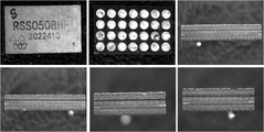
将编号为#001-20220410、#002-20220410、#001-20220419以及#002-20220419的四个依照本实施例进行封装的芯片封装体小样放进温循箱进行温度循环测试。Four chip package samples packaged according to this embodiment, numbered #001-20220410, #002-20220410, #001-20220419 and #002-20220419, were put into a temperature cycle box for temperature cycle test.
1.温度循环条件:1. Temperature cycle conditions:
最低温度:-65℃;Minimum temperature: -65°C;
最高温度:150℃;Maximum temperature: 150°C;
升温时间:1分钟;Heating time: 1 minute;
降温时间:1分钟;Cooling time: 1 minute;
低温保持时间:10分钟;Low temperature holding time: 10 minutes;
高温保持时间:10分钟;High temperature holding time: 10 minutes;
循环次数:500次。Number of cycles: 500 times.
2.温度循环测试过程2. Temperature cycle test process
(1)小样温循前经历过如下操作:对器件底部使用热风枪(设置温度300℃)、距离器件1cm、吹1分钟左右后,将器件取下开始试验。(1) The small sample has undergone the following operations before the temperature cycle: use a heat gun on the bottom of the device (set temperature at 300°C), blow it at a distance of 1cm from the device, and blow it for about 1 minute, then remove the device and start the test.
(2)各引脚接触情况测试:对PVIN/PH引脚对PGND的反向二极管、其余引脚对GND的反向二极管进行测试,反应连接情况,记录测试结果;(2) Test the contact condition of each pin: test the reverse diode of the PVIN/PH pin to PGND, and the reverse diode of the other pins to GND, reflect the connection status, and record the test results;
(3)对器件6个表面进行目检,并使用显微镜拍照,保存照片。(3) Visually inspect the 6 surfaces of the device, take pictures with a microscope, and save the pictures.
3.测试结果3. Test results
图19是样品的引脚定义图。图20和图21分别是四个样品在温度循环测试之前和之后测得的引脚电压值。从图中可以看出,在经过500次高强度温度循环之后,各样品的引脚电压几乎没有发生变化,即其电性能保持稳定。Figure 19 is a pin definition diagram of the sample. Figure 20 and Figure 21 are the pin voltage values measured before and after the temperature cycle test of the four samples respectively. It can be seen from the figure that after 500 high-intensity temperature cycles, the pin voltage of each sample hardly changes, that is, its electrical properties remain stable.
图22至25分别是四个样品在经过500次高强度温度循环之后的显微镜照片。各附图中,左上、中上、右下、左下、中下、右下的子图分别为顶视图、底视图、正视图、后视图、左视图和右视图。从图中可看出,在经过500次高强度温度循环之后,芯片的层状结构保持完好,焊料金球的形态保持完整。Figures 22 to 25 are micrographs of four samples after 500 high-intensity temperature cycles. In each drawing, the upper left, upper middle, lower right, lower left, lower middle, and lower right subfigures are top view, bottom view, front view, rear view, left view, and right view, respectively. It can be seen from the figure that after 500 high-intensity temperature cycles, the layered structure of the chip remains intact, and the shape of the solder gold ball remains intact.
可见,本发明的芯片封装结构具有高可靠性,能够长时间耐受高强度的热冲击而保持结构完整和性能稳定。It can be seen that the chip packaging structure of the present invention has high reliability and can withstand high-intensity thermal shock for a long time while maintaining structural integrity and stable performance.
本发明中的环框4是指预先开设有通孔的预制板框架。该通孔用于围绕芯片2。由于盖板3与环框4为同种BT树脂的预制板,因此在施加于基板之前,可以预先采用粘结或焊接的方式将盖板3与环框4进行紧密的固定。采用粘结方式固定时,本发明优选为采用环氧胶或硅酮胶进行粘结。但在该实施例中,优选为环氧胶焊接的方式进行固定。一方面,由于盖板3与环框4为同种材料,因此二者具有相同的热膨胀系数和耐湿性,因此相互结合之后,在界面处不会产生应力堆积等影响结构稳定性和气密性的缺陷。另一方面,由于盖板3与环框4是预先进行固定的,因此可以预先形成一体化结构,这样,可以在芯片封装之前提前对盖板3与环框4之间粘结或焊接质量进行检测和筛选,使得成品后的芯片封装结构的良率更高。The
并且,为了进一步提高芯片封装结构的散热能力,该实施例中采用硅酮胶填充盖板3与环框4组成的一体化结构与基板之间的空间,以作为固定连接的方式并提高芯片的导热能力。同时,所述盖板的上下两侧均覆盖有金属膜,且盖板内部设置有连接上下金属膜的金属线。由此,由芯片背部产生的热量能够快速、高效的传导至盖板外侧,大大提高了芯片在高温环境下应用的可靠性。Moreover, in order to further improve the heat dissipation capability of the chip packaging structure, in this embodiment, silicone glue is used to fill the space between the integrated structure composed of the
此外,在该实施例中,由于采用了倒装焊接的方式,因此为了进一步提高芯片与基板之间的结构稳固性和耐冲击性能,所述芯片与基板之间的电性连接采用金-金互连的方式。所谓的金-金互连是指基板侧的焊盘顶层和芯片焊盘顶层均为金属金,且采用金球焊接。由此,可以通过无焊料的低温超声焊接方式将芯片的引脚与基板上的焊盘进行焊接。由于采用了金-金互连的方式,能够克服常规的铝制焊盘与金球之间焊接时产生的柯肯达尔效应而使得焊接失效,防止了焊接点的开裂,进一步提高芯片封装环境下的结构稳定性和耐热冲击性能。并且,采用低温无焊料焊接技术,一方面不会因高温焊导致的基板热变形,另一方面,与常规的再流焊接技术相比,不会产生焊料熔化的再流淌,防止了由此可能产生的芯片管脚之间产生异物,增加了器件的良率。In addition, in this embodiment, due to the adoption of flip-chip bonding, in order to further improve the structural stability and impact resistance between the chip and the substrate, the electrical connection between the chip and the substrate adopts gold-gold way of interconnection. The so-called gold-gold interconnection means that the top layer of the pad on the substrate side and the top layer of the chip pad are all metal gold, and are soldered by gold balls. Thus, the leads of the chip and the pads on the substrate can be welded by low-temperature ultrasonic welding without solder. Due to the adoption of the gold-gold interconnection method, it can overcome the Kirkendall effect generated during the welding between the conventional aluminum pad and the gold ball, which makes the welding invalid, prevents the cracking of the welding point, and further improves the chip packaging environment. Excellent structural stability and thermal shock resistance. Moreover, the use of low-temperature solder-free soldering technology, on the one hand, will not cause thermal deformation of the substrate due to high-temperature soldering, and on the other hand, compared with conventional reflow soldering technology, will not cause reflow of solder melting, preventing the possible The resulting foreign matter is generated between the pins of the chip, which increases the yield of the device.
需要说明的是,在该实施例中,图2A示出的环框的通孔是用于容纳一个芯片的情况,但应当理解,本发明并不限于环框的特定尺寸、个数、形状等,也不限于环框内芯片的数量或堆叠数等。It should be noted that, in this embodiment, the through hole of the ring frame shown in FIG. 2A is used to accommodate a chip, but it should be understood that the present invention is not limited to the specific size, number, shape, etc. of the ring frame , and is not limited to the number of chips in the ring frame or the number of stacks, etc.
图2B是本发明的第一实施例的变形实施例的结构示意图。与图2A所示的实施例不同的是,在基板1上且位于环框内,除了固定有芯片2,还固定连接有电容器2-1,该电容器用于对芯片的输入输出信号进行调理。将该电容器2-1可以像芯片2一样通过焊接方式与基板上预设的焊盘进行固定。通过将该电容器2-1与芯片封装在一起,可以使芯片的输入输出性能得到调整或改善而不会改变芯片封装结构的可靠性。Fig. 2B is a schematic structural diagram of a modified embodiment of the first embodiment of the present invention. Different from the embodiment shown in FIG. 2A , on the
本领域技术人员应当理解,该图2B所示的实施例仅是一种示例性实施方式,事实上,除了单个电容器之外,可以根据实际需要将不同的无源器件一并封装成芯片封装结构内部,例如电感、电阻等。Those skilled in the art should understand that the embodiment shown in FIG. 2B is only an exemplary implementation. In fact, in addition to a single capacitor, different passive devices can be packaged together into a chip package structure according to actual needs. Internal, such as inductors, resistors, etc.
图3是本发明的第二实施例的芯片封装结构示意图。该实施例是在环框的一个通孔内容纳两个芯片的情况,即第一芯片21和第二芯片22。当两个芯片封装在一起时,可以节省芯片在电路板上的占用面积并节省成本。通常,第一芯片21和第二芯片22是用于同一电子设备中的不同功能的芯片,例如第一芯片21为传感芯片,第二芯片22为控制芯片。在本发明的其他实施方式中,也可以将三个或三个以上的芯片封装在一起。并且,为了进一步减小芯片的占用面积,还可以采用芯片堆叠技术将多个芯片在竖直方向叠加在一起,这种方式也可以应用于本发明提出的芯片封装结构中。FIG. 3 is a schematic diagram of a chip package structure according to a second embodiment of the present invention. This embodiment is a case where two chips, that is, a
图4是本发明的第三实施例的芯片封装结构示意图。与前一实施例不同的是,该实施例的框架的通孔中设置有一个隔离坝41,用于分隔位于同一芯片封装结构中的两个芯片21、22。该隔离坝作为框架的一部分是与框架整体成形的。通过设置隔离坝41,使得位于同一封装结构中的芯片之间的影响降低,特别是对于高散热、电磁信号强度要求的芯片是至关重要的。FIG. 4 is a schematic diagram of a chip package structure according to a third embodiment of the present invention. Different from the previous embodiment, in this embodiment, an
图5A和图5B分别显示了不具有隔离坝和具有隔离坝的框架的顶面示意图。从图中可看出,所述框架是一体化的结构,可以通过在树脂的预制板上预先形成通孔来形成。Figures 5A and 5B show schematic views of the top surfaces of frames without and with isolation dams, respectively. It can be seen from the figure that the frame is an integrated structure, which can be formed by pre-forming through holes on a resin prefabricated board.
再回到图2A,在图2A所示的实施例中,在预先采用粘结或焊接的方式将盖板3与环框4进行紧密的固定之后,盖板与环框的组成的一体化结构倒扣到具有芯片的基板1上进行密封紧密连接。在该实施例中,所述芯片2与环框4之间、芯片2与盖板3之间、环框4与基板1之间,由硅酮胶或环氧胶填充和粘结。由此,环框4密封连接于基板1上并环绕芯片2,盖板3覆盖于环框4和芯片2之上,并与所述环框4密封连接。Returning to Fig. 2A, in the embodiment shown in Fig. 2A, after the
图6是本发明的第四实施例的芯片封装结构示意图。与第一实施例不同的是,该实施例中,芯片2的背面与盖板3之间,以及环框4与基板1之间,均通过焊接方式连接。图6中示出了芯片2的背面与盖板3之间的第一焊料9,以及环框4与基板1之间的第二焊料10。第一焊料9和第二焊料10的焊接可以同时进行,并且在真空环境下进行,这样使得芯片封装置结构内部具有真空环境,芯片背面产生的热量可以直接通过焊料传到盖板一侧,这对芯片封装结构的散热极为有利。FIG. 6 is a schematic diagram of a chip package structure according to a fourth embodiment of the present invention. Different from the first embodiment, in this embodiment, the connections between the back surface of the
图7A至图10是本发明的芯片封装结构的制造方法的第一实施例的各步骤工序示意图。第一方法实施例包括如下的步骤:FIG. 7A to FIG. 10 are schematic diagrams of each step of the manufacturing method of the chip packaging structure of the first embodiment of the present invention. The first method embodiment includes the following steps:
S1、在基板上固定多个芯片,各芯片相互间隔设置。S1. A plurality of chips are fixed on the substrate, and the chips are arranged at intervals from each other.
由于本发明提出采用三层预制板组成的封装结构,因此本发明特别适合于批量生产。首先在基板1上间隔设置多个芯片。其中图7A是截面图,示意性地示出了两个芯片的情况;图7B是顶视图,示出了4*4矩阵排列的多个芯片的情况。但应理解,为了提高批量生产的效率,在工艺允许的条件下,在一个基板上可以设置更多的芯片。Since the present invention proposes a packaging structure composed of three layers of prefabricated boards, the present invention is particularly suitable for mass production. Firstly, a plurality of chips are arranged at intervals on the
优选的,当芯片数量较多时,由于基板很薄,将所述基板吸附固定于一个第一载舟11上,由此第一载舟可以较好地支撑基板,以利于后续在所述基板上固定所述多个芯片。Preferably, when the number of chips is large, since the substrate is very thin, the substrate is adsorbed and fixed on a
如前所述,基板1的上下表面覆有金属导电层,并通过基板中的预留线路互连。所述芯片2可通过倒装焊接方式固定于基板1上,在倒装焊接之后对基板1和芯片2之间的焊接区域进行下填充工艺,优选为采用导热性和密封性能良好的填充料。As mentioned above, the upper and lower surfaces of the
此外,在该实施例中,所述芯片2与基板1之间的电性连接采用金-金互连的方式,并通过无焊料的低温超声焊接方式将芯片的引脚与基板上的焊盘进行焊接。由于采用了金-金互连的方式,能够克服常规的铝制焊盘与金球之间焊接时产生的柯肯达尔效应而使得焊接失效,防止了焊接点的开裂,进一步提高芯片封装环境下的结构稳定性和耐热冲击性能。并且,采用低温无焊料焊接技术,一方面不会因高温焊导致的基板热变形,另一方面,与常规的再流焊接技术相比,不会产生焊料熔化的再流淌,防止了由此可能产生的芯片管脚之间产生异物,增加了器件的良率。In addition, in this embodiment, the electrical connection between the
S2、在盖板上固定连接环框板。S2. Fix and connect the ring frame plate on the cover plate.
如图8A所示,所述环框板上预先形成有多个通孔,所述通孔的位置与所述多个芯片的位置对应,其尺寸能够容纳并环绕所述芯片。本发明中,盖板3与环框板4为同种BT树脂的预制板。在此步骤中,采用粘结或焊接的方式将盖板3与环框4进行紧密的固定。在该实施例中为焊接的方式进行固定。由于盖板3与环框板4为同种材料,因此二者具有相同的热膨胀系数和耐湿性,因此相互结合之后,在界面处不会产生应力堆积等影响结构稳定性和气密性的缺陷。As shown in FIG. 8A , a plurality of through holes are preformed on the ring frame plate, the positions of the through holes correspond to the positions of the plurality of chips, and the size of the through holes can accommodate and surround the chips. In the present invention, the
该步骤之后,可以对盖板3与环框板4之间粘结或焊接质量进行检测和筛选,对焊料形成有缺陷,或者焊接导致应力集中的环框部分进行标记,以便得有问题的环框不进行后续的工艺,这使得成品后的芯片封装结构的良率更高。After this step, the bonding or welding quality between the
由于该实施例的基板1上固定有多个芯片2,因此,盖板3的尺寸应与基板1相匹配(大致相同),且环框版上的形成的通孔数量与芯片的数量相对应。并且,由于盖板较薄,因此该实施例同样地将所述盖板吸附固定于第二载舟·1上,然后在所述盖板上焊接所述环框板。Since
图8A是截面图,示意性地示出了在盖板3上焊接环框板4的工艺。图8B是仰视立体图,显示了在盖板3上焊接了环框板4的形态。图8C是仰视平面图,示出了4*4矩阵排列的多个通孔的情况。但应理解,为了提高批量生产的效率,在工艺允许的条件下,在一个环框板上可以设置更多的与芯片对应的通孔。FIG. 8A is a cross-sectional view schematically showing the process of welding the
值得一提的是,对于图5B所示的具有隔离坝的环框形态,只需要调整通孔的位置和形状即可。It is worth mentioning that for the ring frame shape with isolation dams shown in Figure 5B, only the position and shape of the through holes need to be adjusted.
S3、将固定有环框板的盖板结合于所述基板上并进行固定,以形成一体化结构,使各所述通孔分别环绕各芯片。S3. Combining and fixing the cover plate on which the ring frame plate is fixed, to form an integrated structure, so that each of the through holes respectively surrounds each chip.
如图9所示,在该实施例中,在环框板4的通孔内及通孔周围涂覆硅酮胶或环氧胶。然后,如图10所示,将所述固定有环框板的盖板上结合于所述基板并进行粘结,使所述芯片2与环框板4之间的空间内、以及所述环框板4与基板1之间,由硅酮胶或环氧胶填充和粘结。As shown in FIG. 9 , in this embodiment, silicone glue or epoxy glue is coated in and around the through hole of the
在芯片封装方法的另一实施例中,如图11所示,将所述固定有环框板的盖板结合于所述基板上并进行固定包括焊接步骤,在芯片2背部及基板的对应于环框的位置涂覆焊料。然后,如图12所示,使用焊接技术将盖板和环框的一体化结构覆盖于基板和芯片上,完成整板焊接。In another embodiment of the chip packaging method, as shown in FIG. 11 , combining the cover plate with the ring frame plate fixed on the substrate and fixing it includes a welding step, and the back of the
S4、切割所述一体化结构,以使各通孔四周形成独立的环框,从而得到多个芯片封装结构。S4. Cutting the integrated structure so that an independent ring frame is formed around each through hole, thereby obtaining multiple chip packaging structures.
如图13所示,在该步骤中,将已经完成封装的整板芯片封装结构进行切割,得到成品的芯片封装结构。As shown in FIG. 13 , in this step, the packaged whole board chip package structure is cut to obtain a finished chip package structure.
需要说明的是,在该步骤S4之前,可以规模化地对整板芯片封装结构)进行筛选,并根据筛选结果对器件成品进行判据。为了满足高可靠性要求,特别是耐热冲击性能的要求,在测试过程中包括有老化的过程。It should be noted that before this step S4, the entire board (chip packaging structure) can be screened on a large scale, and the finished device can be judged according to the screening results. In order to meet the high reliability requirements, especially the requirements of thermal shock resistance, aging process is included in the test process.
在本发明的其他实施例中,步骤S2和S3中对于盖板、环框板和基板之间的结合顺序可以进行适当的改变。In other embodiments of the present invention, the sequence of combining the cover plate, the ring frame plate and the base plate in steps S2 and S3 can be appropriately changed.
图14和图15是将盖板、环框板和基板之间进行固定的不同实施例的示意图。其中显示了三者结合的不同工艺顺序。其中,图14示出了先将所述环框板固定连接于所述具有芯片的基板上,再将所述固定有环框板的基板固定结合于盖板上的工序,图15示出了所述基板、环框板和盖板同时进行固定连接的方式。上述结合方式均可以采用粘结或焊接的方式进行。14 and 15 are schematic diagrams of different embodiments for fixing the cover plate, the ring frame plate and the base plate. It shows different process sequences combining the three. Among them, Fig. 14 shows the process of firstly fixing the ring frame plate to the substrate with the chip, and then fixing the substrate with the ring frame plate fixedly on the cover plate, and Fig. 15 shows The base plate, the ring frame plate and the cover plate are fixedly connected at the same time. All the above-mentioned combining methods can be carried out by bonding or welding.
图16和图17显示了用于对本发明的整板芯片封装结构进行规模化筛选的一体化测试装置的结构示意图。图16是顶视图,图17是截面图。如图16、17所示,该一体化测试装置13包括主板131和位于主板上的与整板芯片封装结构的位置对应的多个限位框132和限位框133内的可伸缩探针133。所述探针133的位置与基板背面的管脚位置相对应。FIG. 16 and FIG. 17 show the structural schematic diagrams of an integrated testing device for large-scale screening of the whole chip packaging structure of the present invention. Fig. 16 is a top view, and Fig. 17 is a cross-sectional view. As shown in Figures 16 and 17, the
图18显示了一体化测试装置对整板芯片封装结构进行测试的示意图。如图18所示,进行测试时,测试装置的限位框顶抵基板1的背面,使探针133对准各基板背面的管脚并回弹,测试装置上的测试电路(未画出)完成测试。FIG. 18 shows a schematic diagram of testing the whole board chip package structure by the integrated testing device. As shown in Figure 18, when testing, the limit frame of the test device is pressed against the back of the
相比于现有技术必须对芯片封装结构的成品器件进行逐一放入测试装置中,本发明无需进行逐一转移、放置等程序,极大地提高了测试的效率。Compared with the prior art where the finished devices of the chip packaging structure must be put into the testing device one by one, the present invention does not need to carry out procedures such as transferring and placing one by one, which greatly improves the efficiency of testing.
此外,在老化时,可以将集成有多个测试探针的一体化老化背夹装置连接于整板芯片封装结构的基板背面的引脚进行,无需对器件进行逐一的转移和放置即可以完成整板芯片封装结构的老化,极大地提高了测试效率。特别是对于本发明的高可靠性芯片封装结构的测试来说,由于测试的次数很多,而采用本发明的整板芯片封装结构的测试装置和测试方法,能够使几乎所有的测试(除了最后一次在切割完成后进行)在整板上进行,这极大地提高了封装后测试和筛选的效率。In addition, during burn-in, the integrated burn-in back clamp device integrated with multiple test probes can be connected to the pins on the back of the substrate of the entire chip package structure, and the entire device can be completed without transferring and placing the devices one by one. The aging of the board-chip package structure greatly improves the test efficiency. Especially for the test of the high-reliability chip packaging structure of the present invention, because the number of times of testing is a lot, the testing device and testing method of the whole board chip packaging structure of the present invention can make almost all tests (except the last time) Carried out after cutting) on the entire board, which greatly improves the efficiency of post-package testing and screening.
以上所述的具体实施例,对本发明的目的、技术方案和有益效果进行了进一步详细说明,应理解的是,以上所述仅为本发明的具体实施例而已,并不用于限制本发明,凡在本发明的精神和原则之内,所做的任何修改、等同替换、改进等,均应包含在本发明的保护范围之内。The specific embodiments described above have further described the purpose, technical solutions and beneficial effects of the present invention in detail. It should be understood that the above descriptions are only specific embodiments of the present invention, and are not intended to limit the present invention. Within the spirit and principles of the present invention, any modifications, equivalent replacements, improvements, etc., shall be included in the protection scope of the present invention.
Claims (18)
Priority Applications (1)
| Application Number | Priority Date | Filing Date | Title |
|---|---|---|---|
| CN202210736606.6A CN114823552B (en) | 2022-06-27 | 2022-06-27 | High-reliability chip packaging structure and packaging method suitable for batch production |
Applications Claiming Priority (1)
| Application Number | Priority Date | Filing Date | Title |
|---|---|---|---|
| CN202210736606.6A CN114823552B (en) | 2022-06-27 | 2022-06-27 | High-reliability chip packaging structure and packaging method suitable for batch production |
Publications (2)
| Publication Number | Publication Date |
|---|---|
| CN114823552A CN114823552A (en) | 2022-07-29 |
| CN114823552B true CN114823552B (en) | 2022-11-11 |
Family
ID=82523538
Family Applications (1)
| Application Number | Title | Priority Date | Filing Date |
|---|---|---|---|
| CN202210736606.6A Active CN114823552B (en) | 2022-06-27 | 2022-06-27 | High-reliability chip packaging structure and packaging method suitable for batch production |
Country Status (1)
| Country | Link |
|---|---|
| CN (1) | CN114823552B (en) |
Families Citing this family (2)
| Publication number | Priority date | Publication date | Assignee | Title |
|---|---|---|---|---|
| CN116031167B (en) * | 2022-12-29 | 2023-09-22 | 声龙(新加坡)私人有限公司 | Chip packaging method and device |
| CN116913864B (en) * | 2023-09-14 | 2023-12-01 | 北京升宇科技有限公司 | High-reliability integrated circuit packaging structure with small junction temperature tolerance and packaging method |
Citations (4)
| Publication number | Priority date | Publication date | Assignee | Title |
|---|---|---|---|---|
| CN101432876A (en) * | 2006-04-27 | 2009-05-13 | 住友电木株式会社 | Semiconductor device and method of manufacturing semiconductor device |
| CN108231700A (en) * | 2016-12-21 | 2018-06-29 | 苏州迈瑞微电子有限公司 | Chip-packaging structure and method |
| CN208207151U (en) * | 2018-06-08 | 2018-12-07 | 湖州慧能机电科技有限公司 | A kind of high-power chip ageing tester |
| CN114300445A (en) * | 2021-12-20 | 2022-04-08 | 湖北三江航天险峰电子信息有限公司 | Radio frequency device packaged by SIP (Session initiation protocol) |
Family Cites Families (2)
| Publication number | Priority date | Publication date | Assignee | Title |
|---|---|---|---|---|
| JP2000223627A (en) * | 1999-01-29 | 2000-08-11 | Nec Corp | Flip chip package |
| DE102012213916A1 (en) * | 2011-11-08 | 2013-05-08 | Robert Bosch Gmbh | Electronic module for a control unit |
-
2022
- 2022-06-27 CN CN202210736606.6A patent/CN114823552B/en active Active
Patent Citations (4)
| Publication number | Priority date | Publication date | Assignee | Title |
|---|---|---|---|---|
| CN101432876A (en) * | 2006-04-27 | 2009-05-13 | 住友电木株式会社 | Semiconductor device and method of manufacturing semiconductor device |
| CN108231700A (en) * | 2016-12-21 | 2018-06-29 | 苏州迈瑞微电子有限公司 | Chip-packaging structure and method |
| CN208207151U (en) * | 2018-06-08 | 2018-12-07 | 湖州慧能机电科技有限公司 | A kind of high-power chip ageing tester |
| CN114300445A (en) * | 2021-12-20 | 2022-04-08 | 湖北三江航天险峰电子信息有限公司 | Radio frequency device packaged by SIP (Session initiation protocol) |
Also Published As
| Publication number | Publication date |
|---|---|
| CN114823552A (en) | 2022-07-29 |
Similar Documents
| Publication | Publication Date | Title |
|---|---|---|
| US5677575A (en) | Semiconductor package having semiconductor chip mounted on board in face-down relation | |
| JP4676640B2 (en) | Intelligent power module package | |
| KR100903063B1 (en) | Low profile ball grid array bga package with exposed die and method of making same | |
| CN114823552B (en) | High-reliability chip packaging structure and packaging method suitable for batch production | |
| JP2013042135A (en) | Power overlay structure with leadframe connections | |
| WO1999044401A1 (en) | Stacking layers containing enclosed ic chips | |
| WO2005004563A1 (en) | Module and method for fabricating the same | |
| TWI648848B (en) | Optical component package structure | |
| US7663254B2 (en) | Semiconductor apparatus and method of manufacturing the same | |
| CN110211884A (en) | Density three-dimensional lamination autoregistration integrated encapsulation method | |
| KR101096330B1 (en) | Package for Semiconductor Devices | |
| CN103094291A (en) | Image sensor packaging structure having double layers of substrates | |
| JPH088354A (en) | Semiconductor device and manufacturing method thereof | |
| CN116913864B (en) | High-reliability integrated circuit packaging structure with small junction temperature tolerance and packaging method | |
| JPH11274375A (en) | Semiconductor device and manufacturing method thereof | |
| CN114823550B (en) | Chip packaging structure and packaging method suitable for batch production | |
| US6415505B1 (en) | Micromachine package fabrication method | |
| CN100424870C (en) | semiconductor module | |
| JPH0846084A (en) | Surface mount semiconductor package, method of manufacturing the same, and semiconductor device | |
| CN108508283A (en) | Electric-field sensor package assembling and its mass manufacturing method | |
| JP2009188392A (en) | Semiconductor device and manufacturing method of semiconductor device | |
| JP3446695B2 (en) | Semiconductor device | |
| CN118553686B (en) | High-reliability chip packaging structure and packaging method for cover plate windowing | |
| JP2002100710A (en) | Semiconductor device and method of manufacturing semiconductor device | |
| JPH09260433A (en) | Method of manufacturing semiconductor device and semiconductor device obtained thereby |
Legal Events
| Date | Code | Title | Description |
|---|---|---|---|
| PB01 | Publication | ||
| PB01 | Publication | ||
| SE01 | Entry into force of request for substantive examination | ||
| SE01 | Entry into force of request for substantive examination | ||
| GR01 | Patent grant | ||
| GR01 | Patent grant |