CN1146973C - Controlled cleavage process - Google Patents
Controlled cleavage process Download PDFInfo
- Publication number
- CN1146973C CN1146973C CNB988049767A CN98804976A CN1146973C CN 1146973 C CN1146973 C CN 1146973C CN B988049767 A CNB988049767 A CN B988049767A CN 98804976 A CN98804976 A CN 98804976A CN 1146973 C CN1146973 C CN 1146973C
- Authority
- CN
- China
- Prior art keywords
- energy
- substrate
- processing
- described processing
- cutting
- Prior art date
- Legal status (The legal status is an assumption and is not a legal conclusion. Google has not performed a legal analysis and makes no representation as to the accuracy of the status listed.)
- Expired - Lifetime
Links
Images


Classifications
-
- H—ELECTRICITY
- H01—ELECTRIC ELEMENTS
- H01L—SEMICONDUCTOR DEVICES NOT COVERED BY CLASS H10
- H01L21/00—Processes or apparatus adapted for the manufacture or treatment of semiconductor or solid state devices or of parts thereof
- H01L21/70—Manufacture or treatment of devices consisting of a plurality of solid state components formed in or on a common substrate or of parts thereof; Manufacture of integrated circuit devices or of parts thereof
- H01L21/71—Manufacture of specific parts of devices defined in group H01L21/70
- H01L21/76—Making of isolation regions between components
- H01L21/762—Dielectric regions, e.g. EPIC dielectric isolation, LOCOS; Trench refilling techniques, SOI technology, use of channel stoppers
- H01L21/7624—Dielectric regions, e.g. EPIC dielectric isolation, LOCOS; Trench refilling techniques, SOI technology, use of channel stoppers using semiconductor on insulator [SOI] technology
- H01L21/76251—Dielectric regions, e.g. EPIC dielectric isolation, LOCOS; Trench refilling techniques, SOI technology, use of channel stoppers using semiconductor on insulator [SOI] technology using bonding techniques
- H01L21/76254—Dielectric regions, e.g. EPIC dielectric isolation, LOCOS; Trench refilling techniques, SOI technology, use of channel stoppers using semiconductor on insulator [SOI] technology using bonding techniques with separation/delamination along an ion implanted layer, e.g. Smart-cut, Unibond
-
- B—PERFORMING OPERATIONS; TRANSPORTING
- B26—HAND CUTTING TOOLS; CUTTING; SEVERING
- B26D—CUTTING; DETAILS COMMON TO MACHINES FOR PERFORATING, PUNCHING, CUTTING-OUT, STAMPING-OUT OR SEVERING
- B26D3/00—Cutting work characterised by the nature of the cut made; Apparatus therefor
- B26D3/28—Splitting layers from work; Mutually separating layers by cutting
-
- B—PERFORMING OPERATIONS; TRANSPORTING
- B26—HAND CUTTING TOOLS; CUTTING; SEVERING
- B26F—PERFORATING; PUNCHING; CUTTING-OUT; STAMPING-OUT; SEVERING BY MEANS OTHER THAN CUTTING
- B26F3/00—Severing by means other than cutting; Apparatus therefor
-
- B—PERFORMING OPERATIONS; TRANSPORTING
- B26—HAND CUTTING TOOLS; CUTTING; SEVERING
- B26F—PERFORATING; PUNCHING; CUTTING-OUT; STAMPING-OUT; SEVERING BY MEANS OTHER THAN CUTTING
- B26F3/00—Severing by means other than cutting; Apparatus therefor
- B26F3/002—Precutting and tensioning or breaking
-
- H—ELECTRICITY
- H01—ELECTRIC ELEMENTS
- H01L—SEMICONDUCTOR DEVICES NOT COVERED BY CLASS H10
- H01L21/00—Processes or apparatus adapted for the manufacture or treatment of semiconductor or solid state devices or of parts thereof
- H01L21/02—Manufacture or treatment of semiconductor devices or of parts thereof
- H01L21/04—Manufacture or treatment of semiconductor devices or of parts thereof the devices having at least one potential-jump barrier or surface barrier, e.g. PN junction, depletion layer or carrier concentration layer
- H01L21/18—Manufacture or treatment of semiconductor devices or of parts thereof the devices having at least one potential-jump barrier or surface barrier, e.g. PN junction, depletion layer or carrier concentration layer the devices having semiconductor bodies comprising elements of Group IV of the Periodic System or AIIIBV compounds with or without impurities, e.g. doping materials
- H01L21/26—Bombardment with radiation
- H01L21/263—Bombardment with radiation with high-energy radiation
- H01L21/265—Bombardment with radiation with high-energy radiation producing ion implantation
- H01L21/26506—Bombardment with radiation with high-energy radiation producing ion implantation in group IV semiconductors
-
- H—ELECTRICITY
- H01—ELECTRIC ELEMENTS
- H01L—SEMICONDUCTOR DEVICES NOT COVERED BY CLASS H10
- H01L27/00—Devices consisting of a plurality of semiconductor or other solid-state components formed in or on a common substrate
- H01L27/02—Devices consisting of a plurality of semiconductor or other solid-state components formed in or on a common substrate including semiconductor components specially adapted for rectifying, oscillating, amplifying or switching and having at least one potential-jump barrier or surface barrier; including integrated passive circuit elements with at least one potential-jump barrier or surface barrier
- H01L27/12—Devices consisting of a plurality of semiconductor or other solid-state components formed in or on a common substrate including semiconductor components specially adapted for rectifying, oscillating, amplifying or switching and having at least one potential-jump barrier or surface barrier; including integrated passive circuit elements with at least one potential-jump barrier or surface barrier the substrate being other than a semiconductor body, e.g. an insulating body
- H01L27/1203—Devices consisting of a plurality of semiconductor or other solid-state components formed in or on a common substrate including semiconductor components specially adapted for rectifying, oscillating, amplifying or switching and having at least one potential-jump barrier or surface barrier; including integrated passive circuit elements with at least one potential-jump barrier or surface barrier the substrate being other than a semiconductor body, e.g. an insulating body the substrate comprising an insulating body on a semiconductor body, e.g. SOI
Landscapes
- Engineering & Computer Science (AREA)
- Physics & Mathematics (AREA)
- Life Sciences & Earth Sciences (AREA)
- Forests & Forestry (AREA)
- Mechanical Engineering (AREA)
- Computer Hardware Design (AREA)
- General Physics & Mathematics (AREA)
- Manufacturing & Machinery (AREA)
- Condensed Matter Physics & Semiconductors (AREA)
- Microelectronics & Electronic Packaging (AREA)
- Power Engineering (AREA)
- High Energy & Nuclear Physics (AREA)
- Health & Medical Sciences (AREA)
- Toxicology (AREA)
- Processing Of Stones Or Stones Resemblance Materials (AREA)
- Mechanical Treatment Of Semiconductor (AREA)
Abstract
A technique for forming a film of material (12) from a donor substrate (10). The technique has a step of introducing energetic particles (22) in a selected manner through a surface of a donor substrate (10) to a selected depth (20) underneath the surface, where the particles have a relatively high concentration to define a donor substrate material (12) above the selected depth and the particles for a pattern at the selected depth. An energy source such as pressurized fluid is directed to a selected region of the donor substrate to initiate a controlled cleaving action of the substrate (10) at the selected depth (20), whereupon the cleaving action provides an expanding cleave front to free the donor material from a remaining portion of the donor substrate.
Description
Cross reference to related application:
(May 12 by tentative application " controlled cleavage processing " in this invention, 1997, application number No, 60/046276), (Feb 19 by application " controlled cleavage processing ", 1998, application number No.09/026115) and by application " controlled cleavage processing " (Feb 19,1998, application number 09/026027 requires priority, the disclosure of these applications at this by the integral body application that combines comprehensively.
Background of invention
The invention relates to the manufacturing of substrate.More specifically, technology provided by the invention is included as in the manufacturing that is used for the silicon of semiconductor integrated circuit-insulator substrate and adopts for example method and apparatus of compressed fluid cutting substrate.But will recognize that the present invention has the applicability of wider scope, it also can be applied to the substrate for other various device usefulness: multilevel integration device, the three-dimension packaging of integrated semiconductor system, photoelectron device, the piezoelectron device, microelectronics mechanical system (" MEMS "), transducer, actuator, solar cell, flat-panel monitor is (as LCD, AMLCD), biology and bio-medical instrument, or the like.
Skilled worker or one might rather say has the people of skill utilizing not too useful made useful articles, instrument or device for many years always.In some cases, rely on less element or standard to assemble in many things.On the other hand, not too useful object also can be separated into than junior unit and improve its practicality.These want the common example of separated article to comprise lining based structures such as glass plate, diamond, and semiconductor lining base, etc.
The normal row of these lining based structures utilizes various technology to carry out cutting or separation.In some situation, the lining base can adopt sawing to operate to carry out cutting.Sawing operation generally depends on rotation of blade or instrument, and they cut and wear the lining sill lining sill is separated into two.But this technology is " coarse " usually extremely, generally can not be used for providing accurately at the lining base of making meticulous instrument and assembly cutting apart.In addition, sawing operation often is difficult to separate or cuts extremely hard and/or frangible material for example diamond or glass.
Correspondingly developed and utilized the cutting measure to separate these technology rigid and/or friable material.For example, in diamond cut, very strong directional heat/mechanical pulsing preferentially guided to be become along diamond one crystal plane.This heat/mechanical pulsing causes the cutting wave surface to propagate along the primary crystallization face usually, and this moment is when coming heat/mechanical pulsing energy level since then to surpass along the fracture energy level of selected crystal face or cutting taking place.
In glass-cutting, usually be on generally rightly for a preferred direction on amorphous glass material, to add the line of quarter with application tool.This line causes the higher stress district that surrounds the amorphous glass material.The mechanical force in addition in the both sides of line, this increases along the stress of this line up to mostly along the glass materials fracture of this line.The cutting process of glass is finished in this fracture, and it can be used to comprise in the various application of family expenses.
Though above-mentioned technology is to be satisfied with mostly in being applied to cutting diamond or family expenses glass, they then have critical limitations in the manufacturing of very little labyrinth or meticulous workpiece.For example say that above technology often " very coarse " can not be with high-precision applications in the manufacturing of the lathe of small and exquisite precision, electronic installation.In addition, above technology can be used for separating a big flat glass by another, but often to by bigger lining base separation or to peel film then invalid.And above-mentioned technology may usually cause not only one the edge cutting wave surface of Different Plane interface slightly, and this uses for accurate cutting is extremely undesirable.
See by above-mentioned, wish worthwhile and effective technology on a kind of cost by the basic separating film material of lining.
Summary of the invention
According to the invention provides the basic improvement technology of removing the film wadding of controlled cleavage operation cause lining that a kind of employing utilizes compressed fluid or fluid to spray.This technology makes the cutting that can start lining base when using single or a plurality of cuttings district by the condition of utilizing controlled energy (for example spatial distribution) and selecting handle so that can excite the cutting wave surface and make it propagate cause lining base removal thin-film material by the lining base.
In a specific embodiment, the present invention proposes to utilize with compressed fluid and does the controlled cleavage processing is formed thin-film material by raw material lining base processing.This processing (for example comprises the guiding high energy particle, charged or neutral molecule with enough kinetic energy, atom, or electronics) selected depth under the surface of the surface by raw material lining base, particle is determined the above raw material of this selected depth for quite high concentration and is served as a contrast the thickness of sill (film that for example can separate material) here.Be cutting raw material lining sill, the method provides energy to select the zone to raw material lining base one, starts the controlled cleavage operation in raw material lining base, by being this cutting operation to be done to become utilize the remainder release raw material of propagating branchs wave surface cause raw material lining base.
Among most of embodiment, the startup of cutting is to rely on to make material stand the fracture of a material in the zone with enough energy, causes the cutting wave surface, and uncontrolled fragmentation of unlikely generation or explosion.This cutting wave surface forms can (E
c) usually must make it to be lower than each regional massive material energy to failure (E
Mat) to avoid pulverizing or explosive material.Directional energy pulse vector in the diamond cut or the line in the glass-cutting be for example wherein the cutting energy be lowered to make can controlled generation and propagate the device of cutting wave surface.The cutting wave surface is from as a higher stress district, and then in case produced, and it is propagated needs more low-yield this promoter region cutting material that comes further by fracture.Propagate the required energy of cutting wave surface and be called as cutting wave surface propagation energy (Ep).This relation can be expressed as:
Ec=Ep+[cutting wave surface stress energy]
The realization that controlled cleavage is handled is to rely on along a direction favourable than other all directions to reduce Ep and utilisable energy is restricted to the Ep that is lower than other unwished-for directions.In any cutting was handled, finished on the cutting surface preferably when only handling by an expansion cutting wave surface generation cutting, though many cuttings wave surface acts on too.
Utilize the present invention can realize surpassing numerous advantage of preexist technology.Particularly, the present invention utilizes the condition of controlled energy and selection, preferably serves as a contrast basic cutting thin-film material by the raw material that comprises many material clips tunic.Everything divisional processing is removed the possibility that thin-film material prevents to damage film simultaneously or serves as a contrast basic remainder selectively by the lining base.Correspondingly, remaining lining base section can repeatedly be used further to other application.
In addition, the present invention adopts low relatively temperature to reduce separated film, raw material substrate during the film controlled cleavage is handled or according to the temperature deviation of many material membranes of other embodiment.In most applications, controlled cleavage is handled and for example can be occurred in as other under the room temperature.Bigger material has been paid in this lower temperature behave, and for example cutting and bonding have the material of remarkable different thermal coefficient of expansion with handling tolerance.In further embodiments, the present invention limits energy in the substrate or stress to being lower than the cutting initial energy, and its total elimination produces the possibility of cutting original position at random or wave surface.This reduces the cutting damage that early pre-exists in the technology to be caused (as shrinkage cavity, crystal defect, fracture, the crack, segmentation, the space, excessively coarse).And the present invention also reduces by being higher than infringement that required stress or pressure effect caused and comparing the crystal region that is caused by high energy particle with prior art.
The present invention realizes these and other interests on the meaning of known treatment technology.But can realize further understanding by the declaratives and the listed accompanying drawing of reference back to characteristic of the present invention and advantage.
Listed accompanying drawing is:
Fig. 1~11 are the reduced graph of explanation according to the controlled cleavage technology of embodiments of the invention; With
Figure 12~18 are the simplification view profile of explanation according to the method for formation silicon of the present invention-insulator substrate.
Specific embodiment is described
The invention provides and be used for removing thin-film material and prevent simultaneously may be to the technology of the damage of this thin-film material and/or substrate remainder by substrate.This thin-film material is attached to or can be attached to configuration example such as silicon-insulator wafer on the target substrate.The present invention can better be understood by reference accompanying drawing and following explanation.
1. controlled cleavage technology
Fig. 1 is the view profile according to substrate 10 of the present invention.This figure does not only limit the scope of claim as illustrating.Show that as example substrate 10 is one to comprise the silicon wafer of the material sections 12 that will be removed (separation), it is the film quite uniformly that is obtained by substrate material.Silicon wafer 10 includes upper surface 14, lower surface 16 and thickness 18.Substrate 10 also has first limit (limit 1) and second limit (limit 2) (also will be cited in the accompanying drawing below).Material sections 12 also is included in the thickness 20 in the thickness 18 of silicon wafer.The invention provides the innovative techniques of utilizing following sequence of steps to remove material sections 12.
The upper surface 14 of selecteed high energy particle 22 by silicon wafer is injected into the selected depth of the thickness 20 of the material sections 12 of determining to be called as thin-film material.Various different technologies can be used to inject high energy particle and advance silicon wafer.These technology comprise utilizes for example Applied MaterialsEaton Corporation, the ion injection of Varian company beam line ion injection device etc.Going back using plasma immersion ion injection (" P111 ") technology on the other hand injects.PaulK.Chu, Chung Chan, with Nathan W.Cheung: " plasma immersion ion inject current application " (Semiconductor International, PP.165~172, June, 1996) and P.K.Chu, S.Qin, C.Chan, N.W.Chung, and L.A.Larson: " plasma immersion ion injects the mature technology of owing of semiconductor processing " (MATERIAL SCIENCE ANDENGINEERING REPORTS, A Review Journal, PP.207~280, VolumeR17, Nos.6-7, Nov.30, plasma injection technique example is described 1996), the two at this in conjunction with doing comprehensive reference.And, inject and also can utilize the ion shower to produce.Certainly, the technology that is adopted depends on application.
According to application, generally select less mass particles to reduce the possibility that material sections 12 is damaged.Promptly be exactly that less mass particles is easy to advance to the selected degree of depth and material sections that unlikely damage particle is advanced and passed through by substrate material.For example, this less mass particles (or high energy particle) almost can be any charged (for example plus or minus) and/or neutral atom or molecule, or electronics etc.In a specific embodiment, particle can be comprise the neutral of the ion that resembles hydrogen and isotope ion thereof and so on, the noble gas ion that resembles helium and isotope and so on and neon and/or etc. charge particle.Particle also can be particle and other light atom mass particles that is obtained by for example compound of relief image hydrogen, water vapour, methane and hydrogen compound and so on.On the other hand, particle also can be any combination of above-mentioned particle and/or ion and/or branch subclass and/or former subclass.Particle generally has enough kinetic energy and comes by surface seepage selected degree of depth under the surface.
Utilize hydrogen as the injection class that enters silicon wafer as example, use one group of specified conditions and inject processing.Injection rate is by about 10
15To about 10
18Atom/cm
2Scope in, and preferably this consumption greater than about 10
16Atom/em
2Inject energy by about 1kev extremely in the scope of about 1Mev, and be generally 50kev.Implantation temperature is by approximately-200 to about 600 ℃ scope, is preferably lower than 400 ℃ to prevent a large amount of hydrogen ions scatter and disappear silicon wafer that injection and the possibility of injecting fault and stress.Hydrogen ion can arrive selected depth to be advanced silicon wafer to+/-0.05 micron precision by guiding selectively approximately+/-0.03.Certainly used ion pattern and treatment conditions depend on application.
In fact, injecting particle increases stress or reduces energy to fracture along a plane that is parallel to substrate upper surface in the selected degree of depth.This energy partly depends on kind and the condition injected.These particles reduce the fracture energy level of selected degree of depth substrate.This is with regard to for to have prepared condition at selected depth along the controlled cleavage of injection face.The energy state that injection occurs in the substrate in all inner places is not enough to excite irreversible fracture (promptly separating or cutting) in substrate material.But should point out, inject usually really can substrate cause a certain amount of can be by the defective (as microdefect) that thermal source or the thermal source of heating fast repair of for example heating of heat treatment subsequently.
Fig. 2 is along the simplification energy Figure 200 that injects substrate 10 sections according to of the present invention.This figure only as graphic extension and is not limited the claim scope here.This reduced graph has the vertical axis 201 that the energy level (E) (or auxiliary energy) of the cutting in the substrate is facilitated in statement.Trunnion axis 203 statements are by the degree of depth or the distance of wafer bottom surface to wafer item face.After the injection particle advanced wafer, substrate had the average cutting energy that is represented as E205, and it is the amount along the required energy of the variant section of this wafer depth district's cutting wafer.Cutting energy (Ec) equals the massive material energy to failure (E in the non-injection region
Mat).At the selected degree of depth 20, energy (E
Cz) 207 lower because the particle that injects mainly be disconnect or weaken crystal structure key (i.e. existence by particle causes the stress increase also to make the energy (Ecz) 207 of substrate descend) to be reduced in the required energy of selected deep cut substrate.More low-yield (i.e. the stress of Zeng Jiaing) that the present invention utilizes the selected degree of depth is the cutting film in a controlled manner.
But substrate generally can avoid crossing over possible cutting wave surface or selected depth Z after injecting processing.Defective or " weakness " district.In these situations, cutting generally can't be controlled, and resembles the massive material heterogeneity because they are subjected to, intrinsic stress, the influence of the random variation of defective.Fig. 3 is for crossing over the simplification energy diagram 300 at the cutting wave surface of the injection substrate 10 with these defectives.This Figure 30 0 only as graphic extension and is not limited the claim scope here.This figure has the vertical axis 301 of expression auxiliary energy (E) and represents is exactly that the trunnion axis statement is along the zone of substrate cutting wave surface by the trunnion axis 303 of the distance on substrate limit 1 to limit 2.As shown in the figure, the cutting wave surface has two and is represented as district 1 and 2 zones 305 and 307, district respectively, they have be lower than average cutting can (E
Cz) 207 cutting can (may be because of higher defect density etc. due to).Correspondingly, greatly may cutting handle and promptly begin simultaneously at one of above-mentioned zone or both sides because each zone all have will be low than the peripheral region the cutting energy.
Say the cutting of the indicated substrate of figure below with reference to Fig. 4 and handle example.The simplification item view 400 of cutting wave surface 401,403 of Fig. 4 for propagating by the injection substrate more.The cutting wave surface is in " weak " district's origin on the cutting plane that particularly comprises district 1 and 2.These cutting wave surfaces are as by producing randomly shown in the arrow and propagating.Adopting the restriction of propagating at random between many cuttings wave surface is to have the different cutting wave surfaces edge possibility of the connection of Different Plane slightly, or forms the possibility of explosion, below will do to describe in detail to this.
Fig. 5 is at the view profile 500 of for example distinguishing 1305 and 2307 films that got by the wafer cutting of many cuttings of tool wave surface.This figure only is not construed as limiting the claim scope here as graphic extension.As shown, may to start along the secondary cutting of this film be explosion 311 in the cutting by regional 1 that is connected with cutting from zone 2 in the zone 3309 that is determined along Different Plane slightly.The size that depends on difference 313, this film may not have the enough qualities that are suitable for making substrate used in integrated circuit or other application.Substrate with explosion 311 generally can not be with dealing with.Correspondingly, generally do not wish to adopt many wave surfaces cutting wafer of stochastic regime.May be assigned to Commissariat A 1 with the technology example that stochastic regime forms many cuttings wave surface, the application people of Energie Atomque (France) has introduction among the US patent No.5374564 of MichelBruel (" Bruel ").The Bruel general description comes cutting to inject the technology of wafer with the overall heat treatment (that is whole plane of heat treatment injection) of adopting the thermal excitation diffusion.The overall heat treatment of substrate causes the startup of many cuttings wave surface of propagating independently usually.In a word, Bruel discloses " non-controlled " cutting operation of being undertaken by the cutting operation that is started by overall thermal source and keep, and this may produce unwanted results.These unwanted results relate to some potential problems, and the imperfect connection of for example cutting wave surface make by excessive coarse surface smoothness on the surface of cutting material owing to surpass required amount for the energy level of keeping cutting, and other is all.The present invention relies on the controlled distribution of injecting energy on the substrate or selects to arrange the formation that overcomes cutting wave surface at random.
Fig. 6 is for adopting the simplification sectional drawing of the injection substrate of selecting layout cutting energy according to the present invention.This figure only as graphic extension and does not impose any restrictions the scope of the claim here.Inject wafer and stand the step that the selectivity energy is arranged or located or aim at, be created in the controlled cleavage operation of 603 pairs of material sections 12 of selected depth.In a preferred embodiment, selecteed energy is arranged near the edge or corner regions of the selected depth 403 that occurs in substrate 10.Utilize the energy to supply with pulse.Energy example includes chemical energy source, source of mechanical energy, power supply and heat abstractor or thermal source.Chemical energy source can have multiple different from particle, fluid, gas, or liquid.These chemical energy sources can also be for increase the chemical reaction of stress in material sections.The chemical energy source time that is used as go up to change, change on the space or continuous overflow and introducing.In other embodiment, obtain source of mechanical energy by rotation, that move, compression, expansion or hyperacoustic energy.The source of mechanical energy time that can be used as go up to change, change on the space or continuous overflow and introducing.In further embodiments, select power supply by added voltage or the electromagnetic field that adds, the time that is used as goes up the overflow that changes, changes on the space and introduces.In also having some embodiment, select heat energy or source of heat release by radiation, convection current or conduction.This thermal source can be by various as photoelectron beam, and fluid sprays, the liquid jet, and gas blowing, electricity/magnetic field, electron beam, heat-electric heating is selected in the heating furnace etc.Source of heat release can be sprayed by fluid, the liquid jet, and gas blowing, cryogen, supercool is liquid but, and heat-electric cooling device is selected in electricity/magnetic field etc.Similar with previous embodiment, thermal source also is to be introduced into as change on last change of time, the space, continuous overflow.Also have, any in the foregoing description all can be carried out combination or separation according to application.The pattern of certainly, used energy depends on application.
Fig. 6 is for adopting the simplification view profile of the injection substrate of selecting layout cutting energy according to the present invention.This figure only as graphic extension and does not impose any restrictions the scope of the claim here.Inject the step that wafer stands selectivity energy layout 601 or location or aiming, be provided at the controlled cleavage operation of the material sections 12 of selected depth 603.In a preferred embodiment, selection can arrange that 607 occur in the edge or the corner regions vicinity of the selected depth 603 of substrate 10.Utilize the energy that pulse is provided.The example of the various energy includes chemical energy source, source of mechanical energy, power supply and the source of heat release energy.Chemical energy source can comprise various as particle, fluid, gas or liquid.These chemical energy sources may comprise that also chemical reaction is to increase the stress in the material sections.Chemical energy source goes up as the time and changes on change, the space or continuous overflow ground introducing.In a further embodiment, can be by rotation, move, compression, expansion or ultrasonic energy obtain source of mechanical energy.This source of mechanical energy time that is used as goes up and changes on change, the space or continuous overflow introducing.In some embodiment are arranged again, pressurize or institute adds electromagnetic field and selects power supply, the time that is used as goes up and changes, changes on the space or continuous overflow is introduced.In other embodiment, thermal source or source of heat release are by selecting in radiation, convection current or the conduction.This thermal source can be by selections such as photoelectron beam, fluid injection, the liquid jet, gas blowing, electricity/magnetic field, electron beam, heat-heating, heating furnaces.Source of heat release can be by the but selections such as liquid, heat-electric cooling device, electricity/magnetic field of fluid injection, the liquid jet, gas blowing, cryogen, supercool.Be similar to the embodiment of front, the thermal source time that is used as goes up and changes on change, the air or continuous overflow introducing.Have again, any the foregoing description can be made up or separate according to using.Certain used energy also depends on application.
In a specific embodiment, can be that pressurized fluid sprays (for example compression) according to the embodiments of the invention energy.Fig. 6 A shows that being used to carry out controlled cleavage according to one embodiment of the invention handles the simplification view profile that sprays fluid from fluid tip 608.The marginal zone that fluid sprays 407 (or the liquid jet or gas blowings) impact substrate 10 is handled by cutting with startup.Fluid by the fluid source injection that is compressed or pressurizes is led to the zone of the selected degree of depth 603 so that utilize as mechanical, chemical, the hot affair from substrate 10 cuttings one thickness of material district 12.As shown, fluid sprays substrate 10 is separated in the selected degree of depth 603 district 609 spaced apart from each other and districts 611.This fluid sprays and also can be adjusted to start and keep controlled cleavage processing cause substrate 10 parting materials 12.Depend on application, fluid sprays to be regulated on direction, place and amplitude and reaches desirable controlled cleavage processing.It can be the combination of the liquid jet or gas blowing or liquid and gas that this fluid sprays.
In a preferred embodiment, this energy can be pressure source for example static state be compressed fluid.Fig. 6 B shows the simplification section diagrammatic sketch according to the compressed fluid source 607 of one embodiment of the invention.Compressed fluid source 607 (for example compressed liquid, Compressed Gas) is added to around substrate 10 or the sealed chamber 621 at edge.As shown, this chamber is sealed by device 623, and it encircles 625 sealings such as grade by for example O shape, and centers on the outward flange of substrate.The pressure that is maintained Pc that this chamber has the marginal zone that is added to substrate 10 starts the controlled cleavage processing with the selected depth at injection material.The outer surface of substrate or positive being retained as can be for example 1 atmospheric pressure or lower pressure P A of ambient pressure.Have pressure differential between interior higher pressure of this chamber and the ambient pressure.This pressure reduction applies active force to the injection region of the selected degree of depth 603.A little less than the injection region of the selected degree of depth structurally comprises that than the peripheral region any bonding pad.Apply active force by pressure reduction and handle startup until controlled cleavage.Controlled cleavage is handled by substrate material 611 parting material thickness 609 so that in the selected degree of depth by substrate material release liner thickness.In addition, pressure P C forces material sections 12 to be separated by substrate material 611 with " leverage ".During cutting was handled, the pressure in the chamber also can be conditioned and start and keep controlled cleavage and handle cause substrate 10 parting materials 12.Depend on application, can raise seamless power in amplitude and realize desirable controlled cleavage processing.This fluid pressure can be obtained by the combination of liquid or gas or liquid and gas.
In a specific embodiment, the invention provides the cutting of a controlled propagation.This controlled propagation cutting is adopted a plurality of continuous impulses to start and is propagated cutting mostly and handle 700, as indicated in Fig. 7.This figure only as graphic extension and does not limit the claim scope here.As shown, in substrate edge guiding pulse, propagate cutting wave surface cause substrate to substrate center and remove material layer.In this embodiment, an energy applies a plurality of pulses (being pulse 1,2 and 3) to substrate continuously.The edge 703 that pulse 1701 is guided substrate starts the cutting operation.Pulse 2705 also is guided in a lateral edges 707 of pulse 1 to expand this cutting wave surface.Pulse 3709 is guided opposite edges 711 further by the substrate separation material layer along expansion cutting wave surface.The combination of these pulses provides the operation 713 of being made the controlled cleavage material layer by substrate.
The serve as reasons simplified illustration of energy 800 of the pulse choice among the front embodiment that does the controlled propagation cutting of Fig. 8.This figure only as graphic extension and does not limit the claim scope here.As shown, pulse 1 has the energy level that surpasses average cutting energy (E), is used to start cutting operation institute energy requirement.The cutting operation is kept or supported to pulse 2 and 3 utilizations along the cutting wave surface than low-lying level.In a specific embodiment, this pulse is a laser pulse, clashes into selected zone and the thermal pulse gradient of beam by the PULSE HEATING substrate here and causes the collaborative cutting formation that generates single cutting wave surface or the additional stress of Propagation of Energy of surpassing.In a preferred embodiment, the bump beam side by side heats and causes the thermal pulse gradient, and it surpasses the cutting energy and forms and Propagation of Energy.Preferablely be, the bump beam cools off simultaneously and causes the thermal pulse gradient, and it surpasses cutting and can form or Propagation of Energy.
Randomly, the intrinsic energy state of substrate or stress can be promoted towards operating required energy level for the startup cutting globally, but are not enough to start the cutting operation according to of the present invention before to substrate-guided a plurality of continuous impulses.The overall energy state of substrate can be utilized the various energy for example chemistry, machinery, heat (source of heat release or thermal source) or electric, independent or combined rising or reduction.Chemical energy source can have various forms such as particle, fluid, gas or liquid.These energy can comprise that also chemical reaction increases the stress in the material sections.Chemical energy source is used as in time and changes, to change on the space or continuous overflow is quoted.Among other embodiment, obtain source of mechanical energy by rotation, that move, compression, expansion or the ultrasonic energy.This source of mechanical energy can be used as in time and change or continuous overflow introducing on change, the space.In other embodiment, select electric energy by added voltage or added electromagnetic field, be used as in time and change, change on the space or continuous overflow is quoted.In some embodiment that have again, select thermal source or source of heat release by radiation, convection current or conduction.This thermal source can be by selecting in photoelectron beam, fluid injection, the liquid jet, gas blowing, electromagnetic field, electron beam, heat-electric heating and the heating furnace.Source of heat release can by fluid injection, the liquid jet, gas blowing, cryogen, supercool but liquid, heat-electric cooling device, electromagnetic field, or the like in select.With aforementioned implementation of class seemingly, this thermal source is also as changing on temporal change, the space or continuous overflow is used.Have, any above-mentioned enforcement all can be carried out combination or separate, and is decided by applicable cases again.Certainly, the pattern of the energy that adopts also depends on application.As point out that the overall energy increases in the material sections energy level or stress and unlikelyly divides equally operation providing energy to start before starting the controlled cleavage operation in material sections.
In a particular embodiment, the energy level on energy lifting substrate cutting plane surpasses the self-starting that its cutting wave surface Propagation of Energy still is not enough to cause the cutting wave surface.Specifically, heat energy or heat or the source of heat release that do not have heat (as a cooling source) form can be added to globally that substrate increases the energy state of substrate or stress level and unlikely startup cutting by front.On the other hand, the energy also can be electricity, chemistry or mechanical.The substrate material of the directed energy to selected zone provides energy applications to start the cutting wave surface, propagates until thin-film material separated voluntarily by the injection region of substrate.Can adopt various different technologies to start the cutting operation.By the following drawings these technology are described.
Fig. 9 is the simplified illustration according to the energy state 900 of the controlled cleavage operation of the single controlled energy of application of one aspect of the present invention.This figure only illustrates explanation and these claim scope is not limited.In this embodiment, the energy level of substrate or the energy state utilization overall situation energy rise to and are higher than cutting propagation energy state, start the required energy state of cutting wave surface but be lower than.For starting the cutting wave surface, an energy for example laser points to beam with impulse form the edge of substrate to start the cutting operation.On the other hand, this energy also can be one with impulse form coolant to be pointed to the cooling fluid (as liquid, gas) that substrate edge starts cutting operation.The overall situation energy is kept the cutting operation, and this generally need be lower than the energy level of startup energy.
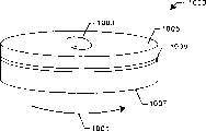
Figure 10 and 11 explanation another aspect of the present invention.Figure 10 is the reduced graph that stands the injection substrate 1000 of revolving force 1001,1003.This image as graphic extension and does not limit the claim scope here.As shown, substrate includes upper surface 1005, the injection region 1009 of the lower surface 1007 and the selected degree of depth.One using energy source light beam or thermal source are increased to the energy level that is higher than cutting wave surface propagation energy state with the overall energy level of substrate, start the required energy state of cutting wave surface but be lower than.This substrate is at the revolving force 1001 that bears rotation clockwise on the upper surface and bear the revolving force of counterclockwise rotation on lower surface, the stress of these 1009 generation startup cutting wave surfaces in the injection region.Also but upper surface bears counterclockwise revolving force and lower surface and bears clockwise revolving force on the other hand.Certainly, the direction of power is nothing serious in this embodiment.
Figure 11 is the reduced graph according to the energy state of the controlled cleavage operation of application revolving force of the present invention.This figure only as graphic extension and does not limit the claim scope here.As noted, the energy level of substrate or energy state are utilized the overall energy (as heat, beam) to be thus lifted to the cutting wave surface and are propagated on the energy state, start the required energy state of cutting wave surface but be lower than.For starting cutting battle array corrugated, the revolving force that the mechanical energy measure for example is added to the injection region starts the cutting wave surface.Specifically, the revolving force that is added to the substrate injection region substrate center produce zero stress and around produce maximum stress, proportional with radius basically.In this example, central starting impulse causes the cutting wave surface cutting substrate of radial dilatation.
Separated material sections provides the silicon materials that deal with usefulness film.Silicon materials have limited surface roughness and are used for the desirable plane characteristic of silicon-on-insulator substrate.In certain embodiments, the surface roughness of the film that is separated is less than about 60nm, or less than about 40nm, or less than the characteristic of about 20nm.Correspondingly, the invention provides the more level and smooth more uniform silicon fiml of comparable prior art.
In a preferred embodiment, the present invention puts into practice being lower than under the temperature used in the prior art.Specifically, the present invention need not to increase as prior art whole substrate temperature and starts and keep cutting operation.At some embodiment to silicon wafer and hydrogen injection, substrate temperature was no more than about 400 ℃ during cutting was handled.On the other hand, substrate temperature also can be no more than about 350 ℃ in cutting is handled.Perhaps also substrate temperature can be passed through for example cooling fluid of source of heat release, cryogen keeps below implantation temperature basically.Correspondingly, the present invention reduced reason at random cutting wave surface excessive releasing energy and the possibility of the unnecessary damage that causes, this has generally improved the surface quality of accompanying surface and/or substrate.Correspondingly, the present invention is provided at higher total output and quality and forms film on the substrate.
Top embodiment is at being illustrated by substrate cutting material film.But substrate may be configured in a workpiece for example on the stiffener before controlled cleavage is handled.This workpiece is connected to the upper surface of substrate or injects the surface so that support structure to film is provided during controlled cleavage is handled.This workpiece can adopt that various combinations or interconnection technique are for example static, adhesion, interatomic interaction is connected to substrate.Some this combination technology is described here.This workpiece can be by dielectric material as quartz, glass, sapphire, silicon nitride, silicon dioxide), electric conducting material (silicon, carborundum, polysilicon, the III/V of family material, metal) and plastics (as polyamides ylidene amines material) make.Certainly, used workpiece type will depend on application.
On the other hand, the substrate with film of wanting separated also can temporarily be configured in before controlled cleavage is handled and be passed on substrate such as stiffener and so on.This passes on substrate and is connected to the upper surface of the substrate with film or injects the surface so that provide support structure to thin-film material during controlled cleavage is handled.This pass on substrate can utilize various different in conjunction with or interconnection technique for example static, bonding, interatomic interaction temporarily are connected to the substrate with film.Some this combination technology is described here.The substrate that passes on can be made by dielectric material (as quartz, glass, sapphire, silicon nitride, silicon dioxide), conductor material (silicon, carborundum, polysilicon, the III/V of family material, metal) and plastics (as polyimide-based material).Certainly, used type of passing on substrate will depend on application.In addition, passing on substrate can be used to after controlled cleavage is handled by the substrate removal thin-film material through cutting.
2. silicon-on-insulator is handled
Processing according to manufacturing silicon one insulator substrate of the present invention can be summarized as follows roughly:
(1) silicon wafer (can be coated) of supplying raw materials with dielectric material;
(2) import particle and advance silicon wafer to the selected depth of determining silicon film thickness;
(3) provide target substrate material (can be coated) with dielectric material;
(4) be connected to the target substrate material and make the raw silicon wafer be attached to the target substrate material by injecting the surface;
(5) increase the overall stress (being energy) of selected depth injection region and do not start cutting operation (choosing wantonly);
(6) utilizing fluid to spray provides the choice of substrate district of stress (being energy) to combination so that start the controlled cleavage operation at selected depth;
(7) provide auxiliary energy to support the controlled cleavage operation so that discharge silicon film thickness (optional) by silicon wafer to the substrate of combination;
(8) finish of the combination of raw silicon wafer to target substrate; With
(9) surface of polished silicon film thickness.
Above sequence of steps provides the energy that is added to the selection zone of multi layer substrate structure according to utilization of the present invention to form the cutting wave surface to start the step of controlled cleavage operation.This setting up procedure is added to substrate with restriction energy begins the cutting processing by controlled way.The propagation of cutting operation subsequently can be undertaken by providing auxiliary energy to support cutting to operate to the choice of substrate zone, and the energy that perhaps is used to the self-starting step provides the further propagation of cutting operation.This sequence of steps only as example and is not limited determined claim scope here.The further details of relevant above-mentioned steps sequence is described with reference to accompanying drawing below.
The simplification view profile of the substrate that Figure 12-18 handles for the manufacturing that stands silicon-insulator wafer according to the present invention.This handles to provide the semiconductor chip that is similar to silicon wafer 2100 to begin, as shown in figure 12.Substrate or raw material include wants separated material sections 2101, is used for the film quite uniformly that is obtained by substrate material.Silicon wafer comprises upper surface 2103, lower surface 2105 and thickness 2107.Material sections also comprises the thickness (Z in the silicon wafer thickness 2107
0).Randomly, the upper surface of dielectric layer 2102 (as silicon nitride, silica, silicon oxynitride) covering substrate.This processing is provided as the innovative techniques that manufacturing silicon-insulator wafer is utilized following steps sequence parting material district 2101.
Selected high energy particle 2109 is injected into the selected depth of the thickness of the material sections of determining to be called as material film by the silicon wafer upper surface.As shown, particle is at the selected degree of depth (Z
0) have desirable concentration 2111.Various technology can be used to inject high energy particle and enter silicon wafer.These technology comprise that utilization for example resembles Applied Materials, Eaton Corporation, the ion injection of the beam line ion injection device that Varian company makes etc.On the other hand, injection also can utilize plasma immersion to inject (" PIII ") technology.In addition, injection also can utilize ion clusters to inject row.Certainly, used technology depends on applicable cases.
According to using, generally select less mass particles to reduce the possibility that material sections is damaged.In other words, less mass particles is easy to advance and arrives the selected degree of depth and can not damage the material sections that particle is advanced and passed through basically by substrate material.For example, this less mass particles (being high energy particle) almost can be any electrically charged (for example plus or minus) and/or neutral atom or molecule or electronics etc.In a particular embodiment, particle can be neutrality and/or the electrically charged particle that comprises hydrogen and isotopic ion, noble gas ion such as helium and isotope and neon.Particle also can be to resemble hydrogen by compound such as gas, water vapour, the particle that methane and other hydrogen compounds obtain, and other light atomic mass particles.On the other hand, particle also can be the combination in any of above-mentioned particle and/or ion and/or molecular forms and/or atomic form.
Handle the step that adopts the silicon wafer that to inject to be connected to a workpiece or aimed wafer, as shown in Figure 13.This workpiece also can be the substrate of various other patterns for example make by dielectric material (as quartz, glass, silicon nitride, silicon dioxide), conductor material (silicon, polysilicon, the III/V of family material, metal) and plastics (as polyimide-based material) those.But this workpiece is a silicon wafer in this example.
In a particular embodiment, silicon wafer utilizes the Low Temperature Heat Treatment step to connect or is fused to together.This low temperature thermal control handle guarantee usually the particle that injects can be in addition inexcessive in material sections, may produce the stress of uncontrolled cutting operation.On the one hand, by handling from carrying out low temperature bond in conjunction with processing.Specifically, a wafer is stripped from so that remove oxidation (promptly a wafer is not oxidized).Cleaning fluid is handled plane of crystal and form the 0-H key on wafer surface.Being used for the solution of clean wafers is exemplified as mixture H
2O
2-H
2SO
4Drier drying crystal wafer surface is so that remove any residual liquid or particle by wafer surface.Undertaken from combining by placing with an oxidized wafer face opposite through clean wafers.
On the other hand, from can being undertaken certainly in conjunction with handling by one of wafer surface of plasma clean combination by activating in conjunction with handling also.Specifically, the plasma clean utilization by gas for example the plasma that obtains of argon, ammonia, neon, water vapour and oxygen activate wafer surface.The wafer surface that is activated 2203 by with another its on have oxide layer and cover 2205 wafer surface and place.These wafers are the sandwich with the wafer face that exposes to the open air.Selecteed pressure is added on the exposed surface of each wafer a wafer is attached to another voluntarily.
On the other hand, adopt the adhesive that is configured on the wafer surface that one wafer is attached on another.This adhesive comprises epoxy resin, polyimide-type materials etc.Can adopt at rotation on glass (spin-on-glass) layer a wafer surface is combined on another the face.These include siloxanes or silicate at rotation on glass (" SOG ") material, and they often mix with alcohol-based solvent etc.SOG can be that a desirable material often needs low temperature (as 150 °~250 ℃) because solidify SOG after being added to wafer surface.
On the other hand, various other cryogenic techniquees also are used to raw wafer is connected to aimed wafer.For example, the static combination technology can be used to two wafers are connected together.Specifically, one or two wafer surface are with electric charge to attract another wafer surface simultaneously.And raw wafer can utilize various known technologies to be fused to aimed wafer.Certainly, used technology depends on application.
After wafer was combined into sandwich 2300, as shown in Figure 14, the method comprised that controlled cleavage operation separate substrates material is to provide the substrate material film 2101 of the insulating barrier 2305 that hides target silicon wafer 2201.The controlled cleavage utilization is selected to distribute or the energy 2301,2303 of the location or the aiming energy carries out to raw material and/or aimed wafer.For example the available energy pulse starts the cutting operation.This pulse utilization comprises that the energy of source of mechanical energy, chemical energy source, source of heat release or thermal source and power supply provides.
The controlled cleavage operation is illustrated by Figure 14 by arbitrary startups of pointing out previously such as technology.For example, the processing and utilizing that is used to start the controlled cleavage operation provides energy 2301,2303 to substrate one selection area so that at the selected depth (Z of substrate
0) start the step of controlled cleavage operation, utilize thus that propagate the cutting wave surface and make that the cutting operation is done to discharge will be by the substrate material part of substrate separation.In a specific embodiment, the method adopts individual pulse to begin the cutting operation, as noted.On the other hand, the method also can utilize the back to arrive the start pulse of the substrate region of selecting with another pulse or consecutive pulses.Perhaps the method also can provide pulse to start the cutting operation of being kept along the energy of substrate scanning.And energy also can be scanned and passes the choice of substrate district and start and/or support controlled cleavage operation.
Randomly, according to the present invention with the energy of substrate material or stress towards operating required energy level and increase for starting cutting, but be not enough to before a pulse or a plurality of continuous impulse are directed into substrate, start the cutting operation.The overall energy state of substrate can utilize various different energy sources for example chemistry,, heat (source of heat release or thermal source) or electricity, raise alone or in combination or reduce.Chemical energy source can comprise particle, fluid, gas or liquid.These energy also can include chemical reaction increases stress in the material sections.This chemical energy source time that is used as goes up and changes on change, the space or continuous overflow introducing.In the additional embodiments, by rotation, move, compression, expansion or the ultrasonic energy obtains source of mechanical energy.This source of mechanical energy time that can be used as goes up and changes on change, the space or continuous overflow introducing.In the embodiment that has again, select the energy by institute's making alive or added electromagnetic field, go up as the time and change, change on the space or continuous overflow is introduced.Also have among some embodiment and select thermal source or source of heat release by radiation, convection current or conduction.This thermal source can be by photoelectron beam, and fluid sprays, the liquid jet, and gas blowing, electricity/magnetic field, electron beam is selected in heat-electric heating and the heating furnace.Source of heat release can be sprayed by fluid, the liquid jet, gas blowing, cryogen, supercool liquid, heat-electric cooling device, electricity/magnetic field, or the like in select.Be similar to the embodiment of front, this thermal source is introduced as variation or continuous overflow on last variation of time, the space.Also have, any the foregoing description all can be made up or separated by using.Nature, the energy pattern that adopts depends on applicable cases.As point out that the overall energy increases energy level in the material sections or stress and unlikelyly providing the cutting operation that starts before starting the controlled cleavage operation in the material sections.
In a preferred embodiment, the method is kept to be lower than and is introduced the temperature that particle advances the temperature of substrate.Among some embodiment, start the step of propagation of cutting operation when the guiding energy during substrate temperature be maintained between-200 to 450 ℃.Substrate temperature also can be maintained at the temperature that is lower than 400 ℃ or is lower than 350 ℃.In a preferred embodiment, the method adopts source of heat release to start and keeps the cutting operation, and this takes place being significantly less than under the condition of room temperature.
Replace in the preferred embodiment one, according to one embodiment of the invention machinery and/or heat energy can be to be pressurized (as compression) fluid to spray.This fluid sprays (or the liquid jet or gas blowing) and impacts the marginal zone 2300 of substrate to start the controlled cleavage operation.Fluid from the fluid energy that compresses or pressurize sprays regional cause substrate 2100 cutting substrate areas 2101 thickness that are introduced in selected depth 2111.This fluid sprays by substrate 2100 and separates 2101, and they are separated from each other in the selected degree of depth 2111.The scalable fluid sprays and starts and keep controlled cleavage and handle cause substrate 2100 parting materials 2101.Depend on applicable cases, can raise the controlled cleavage processing that rectification body sprays the hope that reaches in direction, place and amplitude.
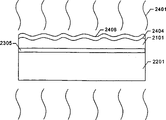
Occur between the film of aimed wafer and material sections, as indicated in Figure 15 according to the last integrating step of some embodiment.Among one embodiment, a silicon wafer has cover layer silicon dioxide, and this is heat growth from the teeth outwards before the cleaning material film.This silicon dioxide also can adopt various other technologies for example chemical vapor deposition form.Hot melt was incorporated into together during silicon dioxide between wafer surface was managed herein.
Among some embodiment, further be pressed onto together and stood oxidation environment 2401 from the oxidized silicon face of aimed wafer or material sections (raw wafer) film.This oxidation environment can be to make steam oxidation, hydroxide or the like in diffusion furnace.The combination of pressure and oxidation environment is fused together two silicon wafers at oxidized surface or interface 2305 places.These embodiment need high temperature (for example 700C) usually.
On the other hand, two silicon faces also can further be pressed onto together and be stood added voltage between two wafers.The temperature that institute's making alive increases wafer is impelled the combination between wafer.This technical limitations in conjunction with the crystal defect amount of introducing silicon wafer during handling substantially need not any mechanical force in conjunction with handling because start between wafer.Certainly, institute's employing technology depends on stress.
Wafer in conjunction with after, silicon one insulator has the target substrate of band silicon materials coverlay and the interlayer oxide layer between target substrate and silicon fiml, also as indicated among Figure 15.The surface of the silicon materials film that separates is usually very coarse, needs polishing.Polishing adopts the combination of grinding and/or polishing technology to carry out.In certain embodiments, it goes up any defective of removal or rough surface to the grinding steps application examples that adopts of release surface as if be rotated in the such technology cause of abrasive material on the release surface.For example can provide this technology by being called " back grinder " so mechanical device that Disco company made.
In addition, chemico-mechanical polishing or complanation (" CMP ") technology also can be polished separation membrane surface, and is represented as Figure 16.In CMP, will be attached to rotation and press the slurry mixture of nog plate (2503) directly to pass to polished surface 2503.This slurry mixture can be sent to polished surface by the aperture that is connected to the thin pulp source.This thin pulp is often for containing for example H of abrasive material and oxidant
2O
2, KIO
3, the solvent of ferric nitrate.Abrasive material usually is Pyrex, titanium dioxide, titanium nitride, aluminium oxide, alchlor, Titanium Nitrate, cerium oxide, silicon dioxide (glue silicon), silicon nitride, carborundum, graphite, all steel stone and their any mixture.This abrasive material mixes in the solvent of deionized water and oxidant etc.Preferably this solvent is acid.
This acid flux material usually in polishing with from the silicon materials effect of wafer.The polyurethanes polishing disk is preferably adopted in polishing.This polishing disk for example is to make the product of selling with trade (brand) name IC-1000 by Rodel.Polishing disk rotates with selected velocity.The carrier head that picks up the aimed wafer that has film applies on the back side of aimed wafer selects big or small pressure so that film is applied selected power.The membrane material amount for selecting is haply removed in polishing, and this is for providing smooth relatively film surface 2601, as showing among Figure 17 with reprocessing.
In certain embodiments, oxide film 2406 covers the material membrane of coverage goal wafer, as shown in Figure 15.Form this oxide layer in thermal anneal step, it is used for forever material membrane being attached to aimed wafer in the above description.Among these embodiment, the selected adjustment of polishing is at first removed oxide and is polished this film then and finish processing.Certainly, this sequence of steps depends on concrete application.
In a specific embodiment, silicon-insulator substrate stands series of processing steps for forming integrated circuit thereon.These treatment steps are introduced in (Vol2, Lattice Press, 1990) in S.Wolf " VLSI epoch silicon handle " literary composition, this article at this in conjunction with doing comprehensive reference.The complete wafer part 2700 that includes integrated circuit is shown by Figure 18.As shown, wafer part 2700 comprises efficient apparatus district 2701 and insulation layer 2703.These efficient apparatus are for having the field-effect transistor of source/drain region 2705 and grid 2707 separately.Define a dielectric insulation layer 2709 and cover efficient apparatus so that efficient apparatus and arbitrary cover layer are insulated.
Though above explanation is at silicon wafer, other substrates also can adopt.For example say that substrate almost can be any monocrystalline, polycrystalline or even armorphous substrate.In addition, substrate also can for example silication gallium, gallium nitride (GaN) etc. be made by the III/V material.The substrate of multilayer also can adopt according to the present invention.The substrate of multilayer includes the silicon-on-insulator substrate, the various folder laminations on the semiconductor chip, and many other form substrates.In addition, above embodiment is generally to provide pulse can start the controlled cleavage operation.This pulse can be substituted by the energy of scanning by the choice of substrate zone and start the controlled cleavage operation.Also can scan by the selection area of substrate and safeguard the controlled cleavage operation.The personage that is familiar with in present technique field is readily appreciated that various replacements, modification and the variant that can be applied by the present invention.
Although more than be complete description, can adopt various modifications, replace structure and equivalent specific embodiment.Therefore, above-mentioned explanation and diagram should not be used for limiting category of the present invention, and it is determined by appended claim.
Claims (48)
1, a kind of processing method that is used for forming material membrane by substrate, described processing comprises step:
The surface of particle by substrate directed into next selected depth of described surface, have finite concentration so that determine on the selected degree of depth, to want separated substrate material at the described particle of described selected depth; With
A selection area that provides energy to arrive described substrate is propagated the described material of the cutting described substrate release portion of wave surface cause to start the controlled cleavage operation in selected depth described in the described substrate, described cutting is operated to utilize.
2, the described processing of claim 1 is characterized in that described particle is from being obtained by the source of selecting one group of hydrogen, helium, water vapour, methane, hydrogen compound and other light atom mass particles.
3, the described processing of claim 1 is characterized in that described particle is by choosing in one group of neutral molecule, neutral atom, charged molecule, electrically charged atom and the electronics.
4, the described processing of claim 1 is characterized in that described particle is a high energy.
5, the described processing of claim 1 is characterized in that described high energy particle has enough kinetic energy and penetrates the described selected degree of depth under the described surface of arrival, described surface.
6, the described processing of claim 1 is characterized in that the described step that energy is provided keeps the described material of the described cutting operation described substrate separation of cause so that material membrane to be provided.
7, the described processing of claim 1, it is characterized in that the described step that energy is provided increase the controlled stress in the described material and keep described cutting operation so as by the described material of described substrate separation so that material membrane to be provided.
8, the described processing of claim 1 is characterized in that described guiding step forms one group of atomic link damage of described substrate in described selected depth, strand displacement, weakening and break and the damage of selecting in the chain.
9, the described processing of claim 8 is characterized in that described damage causes the stress in described substrate material.
10, the described processing of claim 8 is characterized in that described damage reduces the ability that described substrate material meets with stresses and do not have the possibility of the described material of cutting.
11, the described processing of claim 1 is characterized in that described propagation cutting wave surface comprises a plurality of cutting wave surfaces.
12, the described processing of claim 1 is characterized in that described guiding step is because of providing described particle to cause the stress of the described material sections of the described degree of depth in described selected depth.
13, the described processing of claim 1 is characterized in that described energy is selecteed from be made up of thermal source, heat abstractor, source of mechanical energy, chemical energy source and power supply one group.
14, the described processing of claim 13 is characterized in that described chemical energy source is provided by particle.
15, the described processing of claim 13 is characterized in that described chemical energy source comprises a chemical reaction.
16, the described processing of claim 13 is characterized in that described chemical energy source is selecteed one group from being changed by fluid source, time that the energy, space change the energy and the energy is formed continuously.
17, the described processing of claim 31 is characterized in that described source of mechanical energy is selecteed from be made up of the rotation energy, the mobile energy, the compression energy, the expansion energy and ultrasonic energy source one group.
18, the described processing of claim 13 is characterized in that described source of mechanical energy is selecteed one group from being changed by fluid source, time that the energy, space change the energy and the energy is formed continuously.
19, the described processing of claim 13 is characterized in that described power supply is selecteed from be made up of voltage source that applies and the calutron that applies one group.
20, the described processing of claim 13 is characterized in that described power supply is selecteed one group from being changed by fluid source, time that the energy, space change the energy and the energy is formed continuously.
21, the described processing of claim 13 is characterized in that described thermal source or described heat abstractor provide energy by radiation, convection current or conduction.
22, the described processing of claim 21 is characterized in that described thermal source is from by photon beam, and fluid sprays, gas blowing, and electron beam, a hot electric heater, selecteed in the group that heating furnace and smelting furnace are formed.
23, the described processing of claim 21 is characterized in that described heat abstractor is from by the liquid jet, gas blowing, and cryogen, supercool is liquid but, and a hot electric cooling device and supercool are but selecteed in the group of gas composition.
24, the described processing of claim 23 is characterized in that described thermal source is selecteed one group from being changed by fluid source, time that the energy, space change the energy and the energy is formed continuously.
25, the described processing of claim 1 is characterized in that during described guiding step, described substrate temperature is maintained at-200 to the temperature range between the 450C.
26, the described processing of claim 1 is characterized in that the described step of energy that provides is maintained at below the temperature that is lower than 400 ℃.
27, the described processing of claim 1 is characterized in that the described step of energy that provides is maintained at below the temperature that is lower than 350 ℃.
28, the described processing of claim 1 is characterized in that described guiding step is the beam line ion implantation step.
29, the described processing of claim 1 is characterized in that described guiding step is the plasma immersion ion implantation step.
30, the described processing of claim 1 comprises that also surface with described surface combination to a target substrate of described substrate is to form the step of a stack of assembly.
31, the described processing of claim 30, electrostatic pressure carries out by applying between described substrate and described target substrate to it is characterized in that described integrating step.
32, the described processing of claim 30, bonding material carries out by applying between described substrate and described target substrate to it is characterized in that described integrating step.
33, the described processing of claim 30 is characterized in that what described integrating step was undertaken by an activated surface between described substrate and described target substrate.
34, the described processing of claim 30 is characterized in that what described integrating step was undertaken by the interatomic bond between described substrate and described target substrate.
35, the described processing of claim 30 is characterized in that what described integrating step was undertaken by the rotation on glass between described substrate and described target substrate.
36, the described processing of claim 30 is characterized in that what described integrating step was undertaken by the polyimides between described substrate and described target substrate.
37, the described processing of claim 1 is characterized in that described substrate is for being made by the material of one group of silicon, diamond, quartz, glass, sapphire, carborundum, dielectric, the III/V of family material, plastics, ceramic material and the selection of multiple stratification substrate.
38, the described processing of claim 1 is characterized in that described surface is the plane.
39, the described processing of claim 1 is characterized in that described surface is bending or annular.
40, the described processing of claim 1 is characterized in that described substrate is a silicon chip, and described silicon chip comprises the overlapping layer of a dielectric material, and described selected depth is below described dielectric material.
41, the described processing of claim 40 is characterized in that described dielectric material is selecteed from the group of being made up of oxide material, nitride material or oxide/nitride material.
42, the described processing of claim 1 is characterized in that described substrate comprises an overlapping layer of electric conducting material.
43, the described processing of claim 42 is characterized in that described electric conducting material is from by the brilliant silicon compounds of metal, many metal levels, aluminium, tungsten, titanium, titanium nitride, Complex, polysilicon, copper, indium tin oxide, silicon compounds, platinum, gold, silver and amorphous silicon.
44, the described processing of claim 1 is characterized in that described guiding step provides homogeneous granules to distribute at described selected depth along a plane of described material area.
45, the described processing of claim 44 is characterized in that described uniform distribution is the uniformity less than 5%.
46, a kind ofly form the method for a material membrane from silicon single crystal wafer, this method includes step:
Hydrogen ion is injected to this subsurface selected depth in a surface by this silicon single crystal wafer, and these hydrogen ions are assembled at this selected depth has a concentration to determine treating removed one deck above this selected depth;
With this surface combination to one workpiece; And
Select the zone to provide a controlled splitting of this selected depth of energy to move for one of this substrate so that this layer separates from this substrate to be enabled in this substrate.
47, a kind ofly form the method for a material membrane from silicon single crystal wafer, this method includes step:
Hydrogen ion is injected to this subsurface selected depth in a surface by this silicon single crystal wafer, and these hydrogen ions are assembled at this selected depth has a concentration to determine treating removed one deck above this selected depth; And
One of this substrate select regional guidance one high-pressure injection fluid with a controlled splitting action of this selected depth of being enabled in this substrate so that this layer separate from this substrate.
48, the described method of claim 47 is characterized in that this high-pressure injection fluid is heated to more than the chip temperature of this silicon single crystal wafer.
Applications Claiming Priority (6)
| Application Number | Priority Date | Filing Date | Title |
|---|---|---|---|
| US4627697P | 1997-05-12 | 1997-05-12 | |
| US60/046,276 | 1997-05-12 | ||
| US09/026,115 US6155909A (en) | 1997-05-12 | 1998-02-19 | Controlled cleavage system using pressurized fluid |
| US09/026,115 | 1998-02-19 | ||
| US09/026,027 | 1998-02-19 | ||
| US09/026,027 US5994207A (en) | 1997-05-12 | 1998-02-19 | Controlled cleavage process using pressurized fluid |
Publications (2)
| Publication Number | Publication Date |
|---|---|
| CN1255237A CN1255237A (en) | 2000-05-31 |
| CN1146973C true CN1146973C (en) | 2004-04-21 |
Family
ID=27362676
Family Applications (1)
| Application Number | Title | Priority Date | Filing Date |
|---|---|---|---|
| CNB988049767A Expired - Lifetime CN1146973C (en) | 1997-05-12 | 1998-05-11 | Controlled cleavage process |
Country Status (6)
| Country | Link |
|---|---|
| EP (1) | EP0995227A4 (en) |
| JP (1) | JP2001525991A (en) |
| CN (1) | CN1146973C (en) |
| AU (1) | AU7685198A (en) |
| CA (1) | CA2290104A1 (en) |
| WO (1) | WO1998052216A1 (en) |
Families Citing this family (48)
| Publication number | Priority date | Publication date | Assignee | Title |
|---|---|---|---|---|
| SG87916A1 (en) | 1997-12-26 | 2002-04-16 | Canon Kk | Sample separating apparatus and method, and substrate manufacturing method |
| US6383890B2 (en) | 1997-12-26 | 2002-05-07 | Canon Kabushiki Kaisha | Wafer bonding method, apparatus and vacuum chuck |
| US6540861B2 (en) * | 1998-04-01 | 2003-04-01 | Canon Kabushiki Kaisha | Member separating apparatus and processing apparatus |
| JP2000349264A (en) | 1998-12-04 | 2000-12-15 | Canon Inc | Method for manufacturing, use and utilizing method of semiconductor wafer |
| JP4365920B2 (en) * | 1999-02-02 | 2009-11-18 | キヤノン株式会社 | Separation method and semiconductor substrate manufacturing method |
| US6468923B1 (en) | 1999-03-26 | 2002-10-22 | Canon Kabushiki Kaisha | Method of producing semiconductor member |
| FR2795865B1 (en) * | 1999-06-30 | 2001-08-17 | Commissariat Energie Atomique | METHOD FOR MAKING A THIN FILM USING PRESSURIZATION |
| FR2796491B1 (en) | 1999-07-12 | 2001-08-31 | Commissariat Energie Atomique | METHOD FOR TAKING OFF TWO ELEMENTS AND DEVICE FOR IMPLEMENTING SAME |
| FR2797347B1 (en) * | 1999-08-04 | 2001-11-23 | Commissariat Energie Atomique | METHOD FOR TRANSFERRING A THIN FILM HAVING A SURFRAGILILIZATION STEP |
| JP2003506883A (en) * | 1999-08-10 | 2003-02-18 | シリコン ジェネシス コーポレイション | Cleavage process for manufacturing multi-layer substrates with low implant dose |
| US6653209B1 (en) | 1999-09-30 | 2003-11-25 | Canon Kabushiki Kaisha | Method of producing silicon thin film, method of constructing SOI substrate and semiconductor device |
| FR2809867B1 (en) * | 2000-05-30 | 2003-10-24 | Commissariat Energie Atomique | FRAGILE SUBSTRATE AND METHOD FOR MANUFACTURING SUCH SUBSTRATE |
| FR2811807B1 (en) * | 2000-07-12 | 2003-07-04 | Commissariat Energie Atomique | METHOD OF CUTTING A BLOCK OF MATERIAL AND FORMING A THIN FILM |
| JP2002075917A (en) | 2000-08-25 | 2002-03-15 | Canon Inc | Device and method for separating sample |
| FR2817395B1 (en) | 2000-11-27 | 2003-10-31 | Soitec Silicon On Insulator | METHOD FOR MANUFACTURING A SUBSTRATE, IN PARTICULAR FOR OPTICS, ELECTRONICS OR OPTOELECTRONICS AND SUBSTRATE OBTAINED THEREBY |
| FR2818010B1 (en) * | 2000-12-08 | 2003-09-05 | Commissariat Energie Atomique | METHOD OF MAKING A THIN LAYER INVOLVING THE INTRODUCTION OF GAS SPECIES |
| FR2819099B1 (en) * | 2000-12-28 | 2003-09-26 | Commissariat Energie Atomique | METHOD FOR PRODUCING A STACKED STRUCTURE |
| JP4803884B2 (en) * | 2001-01-31 | 2011-10-26 | キヤノン株式会社 | Method for manufacturing thin film semiconductor device |
| JP2002305293A (en) | 2001-04-06 | 2002-10-18 | Canon Inc | Method of manufacturing semiconductor member, and method of manufacturing semiconductor device |
| US6770966B2 (en) * | 2001-07-31 | 2004-08-03 | Intel Corporation | Electronic assembly including a die having an integrated circuit and a layer of diamond to transfer heat |
| TW558743B (en) | 2001-08-22 | 2003-10-21 | Semiconductor Energy Lab | Peeling method and method of manufacturing semiconductor device |
| FR2834380B1 (en) | 2002-01-03 | 2005-02-18 | Soitec Silicon On Insulator | DEVICE FOR CUTTING LAYER OF SUBSTRATE, AND ASSOCIATED METHOD |
| FR2847714B1 (en) * | 2002-11-27 | 2005-02-18 | Soitec Silicon On Insulator | SEMICONDUCTOR WAFER RECOVERY METHOD AND DEVICE |
| TWI233154B (en) | 2002-12-06 | 2005-05-21 | Soitec Silicon On Insulator | Method for recycling a substrate |
| EP1427002B1 (en) * | 2002-12-06 | 2017-04-12 | Soitec | A method for recycling a substrate using local cutting |
| JP4151421B2 (en) * | 2003-01-23 | 2008-09-17 | セイコーエプソン株式会社 | Device manufacturing method |
| JP2005039114A (en) * | 2003-07-17 | 2005-02-10 | Disco Abrasive Syst Ltd | Semiconductor wafer shifting device |
| JP4526561B2 (en) * | 2004-03-22 | 2010-08-18 | ジングルス・テヒノロギース・アクチェンゲゼルシャフト | Method and apparatus for separating disk-type substrates |
| DE102004041378B4 (en) | 2004-08-26 | 2010-07-08 | Siltronic Ag | Semiconductor wafer with a layered structure with low warp and bow and process for its production |
| DE102005000826A1 (en) | 2005-01-05 | 2006-07-20 | Siltronic Ag | Semiconductor wafer with silicon-germanium layer and method for its production |
| EP1894234B1 (en) | 2005-02-28 | 2021-11-03 | Silicon Genesis Corporation | Substrate stiffening method and system for a layer transfer. |
| JP5064692B2 (en) * | 2006-02-09 | 2012-10-31 | 信越化学工業株式会社 | Manufacturing method of SOI substrate |
| JP5064693B2 (en) * | 2006-02-13 | 2012-10-31 | 信越化学工業株式会社 | Manufacturing method of SOI substrate |
| US8293619B2 (en) * | 2008-08-28 | 2012-10-23 | Silicon Genesis Corporation | Layer transfer of films utilizing controlled propagation |
| JP2008112847A (en) | 2006-10-30 | 2008-05-15 | Shin Etsu Chem Co Ltd | Process for manufacturing single crystal silicon solar cell and single crystal silicon solar cell |
| JP5284576B2 (en) * | 2006-11-10 | 2013-09-11 | 信越化学工業株式会社 | Manufacturing method of semiconductor substrate |
| JP5166745B2 (en) * | 2007-03-07 | 2013-03-21 | 信越化学工業株式会社 | Method for producing single crystal silicon solar cell |
| US20100193900A1 (en) * | 2007-07-13 | 2010-08-05 | National University Corporation Tohoku University | Soi substrate and semiconductor device using an soi substrate |
| JP2010021398A (en) * | 2008-07-11 | 2010-01-28 | Disco Abrasive Syst Ltd | Method of treating wafer |
| US7994064B2 (en) * | 2009-06-15 | 2011-08-09 | Twin Creeks Technologies, Inc. | Selective etch for damage at exfoliated surface |
| WO2013058222A1 (en) * | 2011-10-18 | 2013-04-25 | 富士電機株式会社 | Solid-phase bonded wafer support substrate detachment method and semiconductor device fabrication method |
| FR2995447B1 (en) * | 2012-09-07 | 2014-09-05 | Soitec Silicon On Insulator | METHOD FOR SEPARATING AT LEAST TWO SUBSTRATES ACCORDING TO A CHOSEN INTERFACE |
| JP2014138189A (en) * | 2013-01-16 | 2014-07-28 | Silicon Genesis Corp | Controlled process and resulting device |
| CN103077885B (en) * | 2013-01-31 | 2016-06-01 | 上海新傲科技股份有限公司 | Controlled thining method and semiconducter substrate |
| JP6213046B2 (en) * | 2013-08-21 | 2017-10-18 | 信越半導体株式会社 | Manufacturing method of bonded wafer |
| FR3032555B1 (en) * | 2015-02-10 | 2018-01-19 | Soitec | METHOD FOR DEFERRING A USEFUL LAYER |
| CN104979262B (en) * | 2015-05-14 | 2020-09-22 | 浙江中纳晶微电子科技有限公司 | Wafer separation method |
| CN106529159A (en) * | 2016-10-28 | 2017-03-22 | 山东理工大学 | Calculation method for natural angular frequency of transverse vibration of nanometer chord of piezoelectrically-controlled single atomic chain |
Family Cites Families (16)
| Publication number | Priority date | Publication date | Assignee | Title |
|---|---|---|---|---|
| US4466852A (en) * | 1983-10-27 | 1984-08-21 | At&T Technologies, Inc. | Method and apparatus for demounting wafers |
| DE3803424C2 (en) * | 1988-02-05 | 1995-05-18 | Gsf Forschungszentrum Umwelt | Method for the quantitative, depth-differential analysis of solid samples |
| DE69008927T2 (en) * | 1989-05-08 | 1994-12-01 | Philips Nv | Process for splitting a plate made of brittle material. |
| DE4100526A1 (en) * | 1991-01-10 | 1992-07-16 | Wacker Chemitronic | DEVICE AND METHOD FOR AUTOMATICALLY SEPARATING STACKED DISCS |
| JPH04359518A (en) * | 1991-06-06 | 1992-12-11 | Nec Corp | Manufacture of semiconductor device |
| FR2681472B1 (en) * | 1991-09-18 | 1993-10-29 | Commissariat Energie Atomique | PROCESS FOR PRODUCING THIN FILMS OF SEMICONDUCTOR MATERIAL. |
| DE69233314T2 (en) * | 1991-10-11 | 2005-03-24 | Canon K.K. | Process for the production of semiconductor products |
| US5269880A (en) * | 1992-04-03 | 1993-12-14 | Northern Telecom Limited | Tapering sidewalls of via holes |
| FR2715503B1 (en) * | 1994-01-26 | 1996-04-05 | Commissariat Energie Atomique | Substrate for integrated components comprising a thin layer and its production method. |
| JP3293736B2 (en) * | 1996-02-28 | 2002-06-17 | キヤノン株式会社 | Semiconductor substrate manufacturing method and bonded substrate |
| JP3257580B2 (en) * | 1994-03-10 | 2002-02-18 | キヤノン株式会社 | Manufacturing method of semiconductor substrate |
| FR2725074B1 (en) * | 1994-09-22 | 1996-12-20 | Commissariat Energie Atomique | METHOD FOR MANUFACTURING A STRUCTURE COMPRISING A THIN SEMI-CONDUCTIVE LAYER ON A SUBSTRATE |
| SG65697A1 (en) * | 1996-11-15 | 1999-06-22 | Canon Kk | Process for producing semiconductor article |
| CA2233096C (en) * | 1997-03-26 | 2003-01-07 | Canon Kabushiki Kaisha | Substrate and production method thereof |
| JP3667079B2 (en) * | 1997-03-26 | 2005-07-06 | キヤノン株式会社 | Thin film formation method |
| JP2877800B2 (en) * | 1997-03-27 | 1999-03-31 | キヤノン株式会社 | Method of separating composite member, separated member, separation device, method of manufacturing semiconductor substrate, and semiconductor substrate |
-
1998
- 1998-05-11 AU AU76851/98A patent/AU7685198A/en not_active Abandoned
- 1998-05-11 EP EP98924756A patent/EP0995227A4/en not_active Withdrawn
- 1998-05-11 CA CA002290104A patent/CA2290104A1/en not_active Abandoned
- 1998-05-11 JP JP54937198A patent/JP2001525991A/en active Pending
- 1998-05-11 CN CNB988049767A patent/CN1146973C/en not_active Expired - Lifetime
- 1998-05-11 WO PCT/US1998/009567 patent/WO1998052216A1/en not_active Application Discontinuation
Also Published As
| Publication number | Publication date |
|---|---|
| AU7685198A (en) | 1998-12-08 |
| CN1255237A (en) | 2000-05-31 |
| EP0995227A1 (en) | 2000-04-26 |
| WO1998052216A1 (en) | 1998-11-19 |
| CA2290104A1 (en) | 1998-11-19 |
| JP2001525991A (en) | 2001-12-11 |
| EP0995227A4 (en) | 2000-07-05 |
Similar Documents
| Publication | Publication Date | Title |
|---|---|---|
| CN1146973C (en) | Controlled cleavage process | |
| US6458672B1 (en) | Controlled cleavage process and resulting device using beta annealing | |
| US6582999B2 (en) | Controlled cleavage process using pressurized fluid | |
| US6291313B1 (en) | Method and device for controlled cleaving process | |
| CN105051919A (en) | Techniques for forming optoelectronic devices | |
| US6291314B1 (en) | Controlled cleavage process and device for patterned films using a release layer | |
| US6248649B1 (en) | Controlled cleavage process and device for patterned films using patterned implants | |
| US7776717B2 (en) | Controlled process and resulting device | |
| US9159605B2 (en) | Controlled process and resulting device | |
| JP2014138189A (en) | Controlled process and resulting device |
Legal Events
| Date | Code | Title | Description |
|---|---|---|---|
| C06 | Publication | ||
| PB01 | Publication | ||
| C10 | Entry into substantive examination | ||
| SE01 | Entry into force of request for substantive examination | ||
| C14 | Grant of patent or utility model | ||
| GR01 | Patent grant | ||
| CX01 | Expiry of patent term | ||
| CX01 | Expiry of patent term |
Granted publication date: 20040421 |