Disclosure of Invention
The embodiment of the application provides a charging voltage control method, a charging voltage control device, equipment and a storage medium, and can solve the problem that equipment to be charged in a switch-type charging system is slow in charging speed.
In a first aspect, an embodiment of the present application provides a charging voltage control method, applied to a device to be charged, including:
acquiring a first voltage and a first current; the first voltage is the voltage of a battery in the equipment to be charged, and the first current is the current provided by a switch type charging chip in the equipment to be charged for the battery;
determining an efficiency function of the switch-type charging chip according to the first voltage and the first current;
determining a target voltage according to the efficiency function; the target voltage is the optimal charging voltage provided by the PD adapter for the switch type charging chip;
sending a first instruction according to the target voltage; the first instruction is used for instructing the PD adapter to provide the target voltage for the switch-type charging chip.
In a possible implementation manner of the first aspect, the determining an efficiency function of the switching type charging chip according to the first voltage and the first current includes:
controlling the PD adapter to provide a plurality of second voltages for the switch-type charging chip;
calculating the working efficiency of the switch type charging chip corresponding to each second voltage according to the first voltage, the first current and the plurality of second voltages;
and bringing all the second voltages and all the working efficiencies into a preset coordinate system to obtain the efficiency function.
In a possible implementation manner of the first aspect, the calculating, according to the first voltage, the first current, and a plurality of second voltages, an operating efficiency of the switch-type charging chip corresponding to each of the second voltages includes:
determining a second current according to the second voltage, wherein the second current is a current provided by the PD adapter for the switch-type charging chip;
and substituting the first voltage, the first current, the second voltage and the second current into a first calculation formula to obtain the working efficiency.
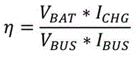
In a possible implementation manner of the first aspect, the first calculation formula is:
wherein,
the efficiency of the operation is expressed in terms of,
is representative of the first voltage,
is representative of the first current,
is representative of the second current of the plurality of current flows,
representing the second voltage.
In a possible implementation manner of the first aspect, the determining an efficiency function of the switch-type charging chip according to the first voltage and the first current includes:
the efficiency function is determined in a database from the first voltage and the first current.
In one possible implementation manner of the first aspect, the charging voltage control method further includes:
acquiring a plurality of groups of charging parameters, wherein each group of charging parameters comprises a first voltage and a first current;
determining an efficiency function corresponding to each group of the charging parameters;
and associating each group of the charging parameters with each efficiency function and storing the parameters in the database.
In a possible implementation manner of the first aspect, the determining a target voltage according to the efficiency curve includes:
carrying out derivation on the efficiency function to obtain a derivative function of the efficiency function;
and determining the voltage when the derivative function is equal to zero as the target voltage.
In a second aspect, an embodiment of the present application provides a charging voltage control apparatus, applied to a device to be charged, including:
the acquisition module is used for acquiring a first voltage and a first current; the first voltage is the voltage of a battery in the equipment to be charged, and the first current is the current provided by a switch type charging chip in the equipment to be charged for the battery;
an efficiency function determination module for determining an efficiency function of the switch-type charging chip according to the first voltage and the first current;
the target voltage determining module is used for determining a target voltage according to the efficiency function; the target voltage is the optimal charging voltage provided by the PD adapter for the switch type charging chip;
the instruction sending module is used for sending a first instruction according to the target voltage; the first instruction is used for instructing the PD adapter to provide the target voltage for the switch-type charging chip.
In a third aspect, an embodiment of the present application provides a device to be charged, including a switch-type charging chip and a battery, where the switch-type charging chip and the battery are electrically connected, and the switch-type charging chip is configured to perform the method according to any one of the first aspect.
In a fourth aspect, the present application provides a computer-readable storage medium, which stores a computer program, and when the computer program is executed by a switch-type charging chip, the computer program implements the method according to any one of the first aspect.
Compared with the prior art, the embodiment of the application has the advantages that:
the embodiment of the application provides a charging voltage control method, which is applied to equipment to be charged and comprises the following steps: acquiring a first voltage and a first current; the first voltage is the voltage of a battery in the equipment to be charged, and the first current is the current provided by a switch type charging chip in the equipment to be charged for the battery. Determining an efficiency function of the switch-type charging chip based on the first voltage and the first current. Determining a target voltage according to the efficiency function; the target voltage is an optimal charging voltage provided by the PD adapter for the switch type charging chip. Sending a first instruction according to the target voltage; the first instruction is used for instructing the PD adapter to provide the target voltage for the switch-type charging chip. According to the charging voltage control method provided by the embodiment of the application, the efficiency function of the switch type charging chip is determined according to the voltage of the battery in the equipment to be charged and the current provided by the switch type charging chip for the battery. And determining the optimal charging voltage provided by the PD adapter for the switch type charging chip according to the efficiency function of the switch type charging chip, wherein the working efficiency of the switch type charging chip corresponding to the optimal charging voltage is highest. When the working efficiency of the switch type charging chip is the highest, the power loss generated by the switch type charging chip in the charging process is the minimum, so that the power loss of the equipment to be charged is correspondingly reduced, the charging power of the equipment to be charged is further improved, the charging speed is accelerated, and the problem of low charging speed of the equipment to be charged in the switch type charging system is solved.
It is understood that the beneficial effects of the second to fourth aspects can be seen from the description of the first aspect, and are not described herein again.
Detailed Description
In the following description, for purposes of explanation and not limitation, specific details are set forth, such as particular system structures, techniques, etc. in order to provide a thorough understanding of the embodiments of the present application. It will be apparent, however, to one skilled in the art that the present application may be practiced in other embodiments that depart from these specific details. In other instances, detailed descriptions of well-known systems, devices, circuits, and methods are omitted so as not to obscure the description of the present application with unnecessary detail.
It will be understood that the terms "comprises" and/or "comprising," when used in this specification and the appended claims, specify the presence of stated features, integers, steps, operations, elements, and/or components, but do not preclude the presence or addition of one or more other features, integers, steps, operations, elements, components, and/or groups thereof.
It should also be understood that the term "and/or" as used in this specification and the appended claims refers to and includes any and all possible combinations of one or more of the associated listed items.
As used in this specification and the appended claims, the term "if" may be interpreted contextually as "when …" or "upon" or "in response to a determination" or "in response to a detection". Similarly, the phrase "if it is determined" or "if a [ described condition or event ] is detected" may be interpreted contextually to mean "upon determining" or "in response to determining" or "upon detecting [ described condition or event ]" or "in response to detecting [ described condition or event ]".
Furthermore, in the description of the present application and the appended claims, the terms "first," "second," "third," and the like are used for distinguishing between descriptions and not necessarily for describing or implying relative importance.
Reference throughout this specification to "one embodiment" or "some embodiments," or the like, means that a particular feature, structure, or characteristic described in connection with the embodiment is included in one or more embodiments of the present application. Thus, appearances of the phrases "in one embodiment," "in some embodiments," "in other embodiments," or the like, in various places throughout this specification are not necessarily all referring to the same embodiment, but rather "one or more but not all embodiments" unless specifically stated otherwise. The terms "comprising," "including," "having," and variations thereof mean "including, but not limited to," unless expressly specified otherwise.
At present, a charging scheme of a device to be charged in a switch-type charging system adopts a fixed voltage mode of a PD, specifically, a fixed voltage output by a PD adapter is reduced to a voltage near a battery voltage based on a switch-type charging chip, and the battery is charged. However, the switch-type charging chip generates power loss in the charging process, when a large current is charged, along with the increase of the power loss generated by the switch-type charging chip, the power loss of the device to be charged is increased, the temperature is also increased, once the power loss or the temperature rise exceeds the power loss limit value or the temperature rise limit of the device to be charged, the switch-type charging chip enters a thermal management state, the charging power of the device to be charged is reduced, even the charging is stopped, and the charging time is further increased.
In view of the above problem, as shown in fig. 1, an embodiment of the present application provides a device to be charged 10, which includes a switch type charging chip 11 and a battery 12, and the switch type charging chip 11 and the battery 12 are electrically connected.
Specifically, in use, the device to be charged 10 is connected to the PD adapter 20, and at this time, the PD adapter 20 is electrically connected to the switch type charging chip 11 in the device to be charged 10, so as to provide the switch type charging chip 11 with the voltage required for charging. During charging, the PD adapter 20 recognizes that the switching type charging chip 11 supplies 5V voltage. The switch type charging chip 11 obtains a first current and a first voltage, the first voltage is the voltage of the battery 12 in the device to be charged 10, and the first current is the current provided by the switch type charging chip 11 in the device to be charged 10 for the battery 12. The switching type charging chip 11 determines an efficiency function of the switching type charging chip 11 according to the first voltage and the first current, wherein the efficiency function of the switching type charging chip 11 represents a relationship between the charging voltage of the switching type charging chip 11 and the operating efficiency of the switching type charging chip 11. The switching type charging chip 11 determines a target voltage according to the efficiency function, where the target voltage is an optimal charging voltage provided by the PD adapter 20 for the switching type charging chip 11, and the working efficiency of the switching type charging chip 11 corresponding to the optimal charging voltage is the highest. The switching type charging chip 11 sends a first instruction according to the target voltage, and the first instruction is used for instructing the PD adapter 20 to provide the target voltage for the switching type charging chip 11, so that the switching type charging chip 11 is always at the highest working efficiency in the charging process. When the working efficiency of the switch-type charging chip 11 is the highest, the power loss generated by the switch-type charging chip 11 in the charging process is the smallest, so that the power loss of the device to be charged 10 is correspondingly reduced, the charging power of the device to be charged 10 is further improved, the charging speed is accelerated, and the problem of low charging speed of the device to be charged 10 in the switch-type charging system is solved.
Note that the PD adaptor 20 can Supply a Programmable Power Supply (PPS).
As shown in fig. 2, an embodiment of the present application further provides a charging voltage control method applied to a device to be charged, including steps S201 to S204.
S201, acquiring a first voltage and a first current. The first voltage is the voltage of a battery in the equipment to be charged, and the first current is the current provided by a switch type charging chip in the equipment to be charged for the battery.
Specifically, the first current is obtained by a switch-type charging chip in the device to be charged, where the first current may be preset by the switch-type charging chip. The first voltage is obtained by a switch-type charging chip connected to the battery. The obtained first current and first voltage are used for subsequently determining an efficiency function of the switch-type charging chip.
And S202, determining an efficiency function of the switch type charging chip according to the first voltage and the first current.
Specifically, because the switch-type charging chip generates power loss during the charging process, the power loss of the device to be charged is correspondingly increased along with the increase of the power loss generated by the switch-type charging chip during the charging process, so that the charging power of the device to be charged is reduced, and even the charging is stopped. In order to minimize the power loss generated by the switch-type charging chip and reduce the power loss of the device to be charged, the switch-type charging chip is always at the highest working efficiency. In order to determine the highest working efficiency of the switch-type charging chip, the application determines an efficiency function of the switch-type charging chip through a first voltage and a first current, wherein the efficiency function of the switch-type charging chip represents the relation between the charging voltage of the switch-type charging chip and the working efficiency of the switch-type charging chip. When the switch type charging chip is at the highest working efficiency, a charging voltage, namely an optimal charging voltage, is corresponded at the moment. The PD adapter provides the optimal charging voltage for the switch type charging chip, so that the switch type charging chip is always at the highest working efficiency, the power loss generated by the switch type charging chip is minimized, the power loss of the equipment to be charged is correspondingly reduced, the charging power of the equipment to be charged is improved, and the charging speed is accelerated.
And S203, determining a target voltage according to the efficiency function. Wherein the target voltage is an optimal charging voltage provided by the PD adapter for the switch-type charging chip.
Specifically, the principle of determining the target voltage is to determine the highest operating efficiency of the switch-type charging chip through an efficiency function, for example, at point a in fig. 8, where a voltage corresponding to the highest operating efficiency of the switch-type charging chip is the target voltage. When the switch type charging chip works under the target voltage, the generated power loss is minimum, so that the power loss of the equipment to be charged is correspondingly reduced, the charging power of the equipment to be charged is further improved, and the charging speed is accelerated.
And S204, sending a first command according to the target voltage. Wherein the first instruction is to instruct the PD adapter to provide a target voltage for the switched-mode charging chip.
Specifically, after the target voltage is determined according to the efficiency function, the switching type charging chip instructs the PD adapter to provide the target voltage for the switching type charging chip, specifically, the switching type charging chip informs the PD protocol chip of the required charging voltage through the communication interface, the PD protocol chip communicates with the PD adapter through the PPS protocol, and informs the PD adapter of the required charging voltage of the switching type charging chip, that is, the switching type charging chip sends a first instruction through the PD protocol chip, and after receiving the first instruction, the PD adapter adjusts the output voltage to the target voltage, so that the switching type charging chip is always at the highest working efficiency until the charging is finished. According to the charging voltage control method provided by the embodiment of the application, the efficiency function of the switch type charging chip is determined according to the voltage of the battery in the equipment to be charged and the current provided by the switch type charging chip for the battery. And determining the optimal charging voltage provided by the PD adapter for the switch type charging chip according to the efficiency function of the switch type charging chip, wherein the working efficiency of the switch type charging chip corresponding to the optimal charging voltage is highest. When the working efficiency of the switch type charging chip is the highest, the power loss generated by the switch type charging chip in the charging process is the minimum, so that the power loss of the equipment to be charged is correspondingly reduced, the charging power of the equipment to be charged is further improved, the charging speed is accelerated, and the problem of low charging speed of the equipment to be charged in the switch type charging system is solved.
Illustratively, as shown in fig. 3, step S202 includes step S2021 to step S2023.
And S2021, controlling the PD adapter to provide a plurality of second voltages for the switch type charging chip.
Specifically, the switching type charging chip controls the PD adapter to provide a plurality of second voltages, where the second voltages are charging voltages provided by the PD adapter for the switching type charging chip, and the variation of the operating efficiency of the switching type charging chip is monitored by changing the charging voltages provided by the PD adapter for the switching type charging chip.
Illustratively, the step distance between two second voltages may be 20mV, the first second voltage may be 5V, and the last second voltage may be 12V.
S2022, calculating the operating efficiency of the switch-type charging chip corresponding to each second voltage according to the first voltage, the first current and the plurality of second voltages.
Specifically, the first voltage and the first current are preset to be unchanged, the charging voltage provided by the PD adapter for the switch-type charging chip is changed, the change condition of the working efficiency of the switch-type charging chip is monitored, and the working efficiency of the switch-type charging chip corresponding to each second voltage is calculated.
And S2023, bringing all the second voltages and all the working efficiencies into a preset coordinate system to obtain an efficiency function.
Specifically, the preset coordinate system takes the second voltage as an x-axis and the working efficiency as a y-axis, and the second voltage and the working efficiency are brought into the preset coordinate system in a one-to-one correspondence manner to obtain an efficiency function.
Illustratively, as shown in fig. 4, step S2022 includes steps S20221 to S20222.
And S20221, determining a second current according to the second voltage, wherein the second current is the current provided by the PD adapter for the switch-type charging chip.
Specifically, after the model and the peripheral circuit of the switch-type charging chip are determined, when the charging voltage provided by the PD adapter for the switch-type charging chip changes, the current provided by the PD adapter for the switch-type charging chip also changes, that is, each second voltage corresponds to one second current. When the second voltage changes, the second current correspondingly changes, and the corresponding second current under each second voltage is obtained through the switch type charging chip.
S20222, the first voltage, the first current, the second voltage and the second current are substituted into a first calculation formula to obtain the working efficiency.
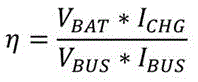
Illustratively, the first calculation formula is:
wherein,
the efficiency of the operation is expressed in terms of,
is representative of the first voltage,
is representative of the first current of the electric current,
is representative of the second current of the current,
representing the second voltage.
Illustratively, as shown in fig. 5, step S202 includes step S2024.
S2024, determining an efficiency function in a database according to the first voltage and the first current.
Specifically, a database is constructed through presetting, and a plurality of data sets are stored in the database, wherein each data set corresponds to an efficiency function, and each data set comprises a first voltage and a first current. After the switch type charging chip acquires the first voltage and the first current, the efficiency function corresponding to the first voltage and the first current can be determined by directly inquiring in a database.
In one embodiment of the present application, a method for creating a database includes: a plurality of sets of charging parameters are obtained, wherein each set of charging parameters comprises a first voltage and a first current. And then determining an efficiency function corresponding to each group of charging parameters. And finally, associating each group of charging parameters with each efficiency function and storing the parameters in a database.
Illustratively, a first set of charging parameters is obtained, assuming a first voltage of 4.0V and a first current of 4A among the charging parameters. The first voltage can be obtained by a battery simulator, and the first current can be preset by a switch type charging chip.
And providing a plurality of second voltages for the switch type charging chip, and simultaneously acquiring a second current which is changed along with the second voltages through the switch type charging chip.
And calculating the working efficiency of the switch type charging chip corresponding to each second voltage according to a first calculation formula to obtain multiple groups of data, wherein each group of data comprises one second voltage and one working efficiency, and determining an efficiency function of the switch type charging chip when the first voltage is 4.0V and the first current is 4A according to the change rule of the multiple groups of data, and the efficiency function of the switch type charging chip when the first voltage is 4.0V and the first current is 4A is shown in fig. 8.
A first set of charging parameters is associated with the efficiency function and stored to a database.
And acquiring a second group of charging parameters, repeating the process to obtain an efficiency function corresponding to the second group of charging parameters, associating the second group of charging parameters with the efficiency function, and storing the second group of charging parameters and the efficiency function in a database. And by analogy, the database is gradually perfected.
Illustratively, as shown in fig. 6, step S203 includes step S2031 to step S2032.
Step S2031, a derivative is performed on the efficiency function to obtain a derivative function of the efficiency function.
In step S2032, the voltage when the derivative function is equal to zero is determined as the target voltage.
Specifically, the highest working efficiency of the switch-type charging chip is the highest point of the efficiency function, so that the highest point of the efficiency function is determined, that is, the target voltage can be determined. According to the method, the highest point of the efficiency function is determined by using a derivation method, and as can be known by referring to fig. 8, the slope of the highest point of the efficiency function is 0, so that the voltage when the derivation function is zero is found to be the target voltage by deriving the efficiency function.
It should be understood that, the sequence numbers of the steps in the foregoing embodiments do not imply an execution sequence, and the execution sequence of each process should be determined by its function and inherent logic, and should not constitute any limitation to the implementation process of the embodiments of the present application.
As shown in fig. 7, an embodiment of the present application further provides a charging voltage control apparatus, applied to a device to be charged, including:
an obtaining module 71, configured to obtain a first voltage and a first current; the first voltage is the voltage of a battery in the equipment to be charged, and the first current is the current provided by a switch type charging chip in the equipment to be charged for the battery.
An efficiency function determining module 72 for determining an efficiency function of the switch-type charging chip based on the first voltage and the first current.
A target voltage determination module 73 for determining a target voltage based on the efficiency function; the target voltage is an optimal charging voltage provided by the PD adapter for the switch type charging chip.
An instruction sending module 74, configured to send a first instruction according to the target voltage; the first instruction is used for instructing the PD adapter to provide the target voltage for the switch-type charging chip.
Specifically, the charging voltage control apparatus provided in the embodiment of the present application determines an efficiency function of the switch type charging chip according to a voltage of a battery in the device to be charged and a current provided by the switch type charging chip for the battery. And determining the optimal charging voltage provided by the PD adapter for the switch type charging chip according to the efficiency function of the switch type charging chip, wherein the working efficiency of the switch type charging chip corresponding to the optimal charging voltage is highest. When the working efficiency of the switch type charging chip is the highest, the power loss generated by the switch type charging chip in the charging process is the minimum, so that the power loss of the equipment to be charged is correspondingly reduced, the charging power of the equipment to be charged is further improved, the charging speed is accelerated, and the problem of low charging speed of the equipment to be charged in the switch type charging system is solved.
In one embodiment of the present application, the efficiency function determination module 72 is further configured to:
controlling the PD adapter to provide a plurality of second voltages for the switch-type charging chip;
calculating the working efficiency of the switch type charging chip corresponding to each second voltage according to the first voltage, the first current and the plurality of second voltages;
and bringing all the second voltages and all the working efficiencies into a preset coordinate system to obtain the efficiency function.
In one embodiment of the present application, the efficiency function determination module 72 is further configured to:
determining a second current according to the second voltage, wherein the second current is the current provided by the PD adapter for the switch-type charging chip;
and substituting the first voltage, the first current, the second voltage and the second current into a first calculation formula to obtain the working efficiency.
In an embodiment of the present application, the first calculation formula is:
wherein,
the efficiency of the operation is expressed in terms of,
is representative of the first voltage,
is representative of the first current,
is representative of the second current of the plurality of current flows,
representing the second voltage.
In one embodiment of the present application, the efficiency function determination module 72 is further configured to:
the efficiency function is determined in a database from the first voltage and the first current.
In one embodiment of the present application, the charging voltage control apparatus further includes:
acquiring a plurality of groups of charging parameters, wherein each group of charging parameters comprises a first voltage and a first current;
determining an efficiency function corresponding to each group of the charging parameters;
and associating each group of the charging parameters with each efficiency function and storing the parameters in the database.
In an embodiment of the present application, the target voltage determining module 73 is further configured to:
carrying out derivation on the efficiency function to obtain a derivative function of the efficiency function;
and determining the voltage when the derivative function is equal to zero as the target voltage.
It will be apparent to those skilled in the art that, for convenience and brevity of description, only the above-mentioned division of the functional units and modules is illustrated, and in practical applications, the above-mentioned function distribution may be performed by different functional units and modules according to needs, that is, the internal structure of the apparatus is divided into different functional units or modules to perform all or part of the above-mentioned functions. Each functional unit and module in the embodiments may be integrated in one processing unit, or each unit may exist alone physically, or two or more units are integrated in one unit, and the integrated unit may be implemented in a form of hardware, or in a form of software functional unit. In addition, specific names of the functional units and modules are only for convenience of distinguishing from each other, and are not used for limiting the protection scope of the present application. For the specific working processes of the units and modules in the system, reference may be made to the corresponding processes in the foregoing method embodiments, which are not described herein again.
An embodiment of the present application further provides a computer-readable storage medium, which stores a computer program, and when the computer program is executed by a switch-type charging chip, the computer program implements the method according to any one of the above.
In the above embodiments, the description of each embodiment has its own emphasis, and reference may be made to the related description of other embodiments for parts that are not described or recited in any embodiment.
The above-mentioned embodiments are only used for illustrating the technical solutions of the present application, and not for limiting the same; although the present application has been described in detail with reference to the foregoing embodiments, it should be understood by those of ordinary skill in the art that: the technical solutions described in the foregoing embodiments may still be modified, or some technical features may be equivalently replaced; such modifications and substitutions do not substantially depart from the spirit and scope of the embodiments of the present application and are intended to be included within the scope of the present application.