CN1140373C - Welding method - Google Patents
Welding method Download PDFInfo
- Publication number
- CN1140373C CN1140373C CNB00122283XA CN00122283A CN1140373C CN 1140373 C CN1140373 C CN 1140373C CN B00122283X A CNB00122283X A CN B00122283XA CN 00122283 A CN00122283 A CN 00122283A CN 1140373 C CN1140373 C CN 1140373C
- Authority
- CN
- China
- Prior art keywords
- flux
- additive
- welding
- component
- solder
- Prior art date
- Legal status (The legal status is an assumption and is not a legal conclusion. Google has not performed a legal analysis and makes no representation as to the accuracy of the status listed.)
- Expired - Fee Related
Links
Images


Classifications
-
- B—PERFORMING OPERATIONS; TRANSPORTING
- B23—MACHINE TOOLS; METAL-WORKING NOT OTHERWISE PROVIDED FOR
- B23K—SOLDERING OR UNSOLDERING; WELDING; CLADDING OR PLATING BY SOLDERING OR WELDING; CUTTING BY APPLYING HEAT LOCALLY, e.g. FLAME CUTTING; WORKING BY LASER BEAM
- B23K31/00—Processes relevant to this subclass, specially adapted for particular articles or purposes, but not covered by any single one of main groups B23K1/00 - B23K28/00
- B23K31/02—Processes relevant to this subclass, specially adapted for particular articles or purposes, but not covered by any single one of main groups B23K1/00 - B23K28/00 relating to soldering or welding
-
- H—ELECTRICITY
- H05—ELECTRIC TECHNIQUES NOT OTHERWISE PROVIDED FOR
- H05K—PRINTED CIRCUITS; CASINGS OR CONSTRUCTIONAL DETAILS OF ELECTRIC APPARATUS; MANUFACTURE OF ASSEMBLAGES OF ELECTRICAL COMPONENTS
- H05K3/00—Apparatus or processes for manufacturing printed circuits
- H05K3/30—Assembling printed circuits with electric components, e.g. with resistors
- H05K3/32—Assembling printed circuits with electric components, e.g. with resistors electrically connecting electric components or wires to printed circuits
- H05K3/34—Assembling printed circuits with electric components, e.g. with resistors electrically connecting electric components or wires to printed circuits by soldering
- H05K3/346—Solder materials or compositions specially adapted therefor
-
- B—PERFORMING OPERATIONS; TRANSPORTING
- B23—MACHINE TOOLS; METAL-WORKING NOT OTHERWISE PROVIDED FOR
- B23K—SOLDERING OR UNSOLDERING; WELDING; CLADDING OR PLATING BY SOLDERING OR WELDING; CUTTING BY APPLYING HEAT LOCALLY, e.g. FLAME CUTTING; WORKING BY LASER BEAM
- B23K2101/00—Articles made by soldering, welding or cutting
- B23K2101/36—Electric or electronic devices
- B23K2101/40—Semiconductor devices
Landscapes
- Engineering & Computer Science (AREA)
- Mechanical Engineering (AREA)
- Manufacturing & Machinery (AREA)
- Microelectronics & Electronic Packaging (AREA)
- Electric Connection Of Electric Components To Printed Circuits (AREA)
Abstract
Description
技术领域technical field
本发明涉及在印刷电路板上焊接部件的方法。The present invention relates to methods of soldering components on printed circuit boards.
背景技术Background technique
在印刷电路板的安装表面焊接部件进行实际安装时,为了防止不润湿(Non-wetting),预先对部件进行预备焊接。经过预备焊接的熔融状态的部件在接近或与前述表面连接的状态下焊接在进行实际安装的前述表面。这种情况下,预备焊剂的组分与焊接时所用焊剂(以下称为本焊剂)相同。When actually mounting components by soldering on the mounting surface of the printed circuit board, the components are preliminarily soldered in order to prevent non-wetting. The pre-welded molten component is welded to the surface to be actually mounted in a state close to or in contact with the surface. In this case, the composition of the preliminary flux is the same as that of the flux used for soldering (hereinafter referred to as this flux).
JP,A7-254780记载了提高连接强度的技术。即记载了以下技术,如图6A所示,用锡含量低于低共熔焊剂(eutectic solder)的高温焊剂(Sn-Pb)作为预备焊剂3对印刷电路板1的Cu安装表面2进行预备焊接。然后,如图6B所示,在该预备焊剂面沾上低共熔焊剂4,用温热的风吹拂低共熔焊剂4进行软熔处理。最后,如图6C所示,使低共熔焊剂4熔融,固定在金属部件5的电极5a的周围,对金属部件5进行焊接。JP, A7-254780 describes a technique for improving connection strength. That is, the following technology is described. As shown in FIG. 6A, a high-temperature solder (Sn-Pb) having a tin content lower than that of eutectic solder is used as a
如图6所示用预备焊剂3进行处理后,用低共熔焊剂4对预备焊剂3的润湿(wetting)情况好于用低共熔焊剂4润湿Cu安装表面2的情况,用预备焊剂进行了处理的连接界面的连接强度大于未用预备焊剂进行处理的界面。图6C中,牢固的连接界面用符号J1表示。After processing with
但是,图6所示构成虽然能够提高连接强度,但现在要求有更大的连接强度。However, although the structure shown in FIG. 6 can improve the connection strength, a larger connection strength is required at present.
特别是从家电的再循环利用角度考虑,即使是用作为用于家电产品的焊接材料的正倍受瞩目的无铅焊剂(1ead free solder)进行焊接,对其连接强度也有更高的要求。Especially from the perspective of recycling of home appliances, even soldering with lead-free solder (1ead free solder), which is attracting attention as a soldering material for home appliances, requires higher connection strength.
发明目的purpose of invention
本发明的目的是提供能够获得优于以往的连接强度的焊接方法。An object of the present invention is to provide a welding method capable of obtaining a connection strength superior to conventional ones.
本发明的焊接方法包括:对安装表面进行预备焊接,然后再焊接部件时,所用预备焊剂的熔点高于焊接部件的本焊剂的熔点,该焊剂至少含有部分安装表面组分和本焊剂组分,在进行过预备焊接的表面用本焊剂进行焊接,The welding method of the present invention includes: performing preparatory welding on the mounting surface, and then when welding the components, the melting point of the prepared flux used is higher than the melting point of the flux for welding the components, and the flux contains at least part of the components of the mounting surface and the flux components, Solder with this flux on the surface that has been prepared for soldering,
其特征在于,所述安装表面为Cu,本焊剂组分为(Sn-Ag-Cu-Bi)、(Sn-Ag系+添加物)、(Sn-Zn系+添加物)、(Sn-Bi系+添加物)、(Sn-In系+添加物)中的任一种,预备焊剂组分为Sn-Cu。It is characterized in that the mounting surface is Cu, and the flux components are (Sn-Ag-Cu-Bi), (Sn-Ag system + additive), (Sn-Zn system + additive), (Sn-Bi system + additives), (Sn-In system + additives), the preparation flux component is Sn-Cu.
本发明的另一焊接方法包括:对部件进行预备焊接,然后再焊到安装表面时,所用预备焊剂的熔点高于焊接部件的本焊剂的熔点,该焊剂至少含有部分部件的焊接部分组分和本焊剂组分,用本焊剂将进行过预备焊接处理的部件焊接到安装表面,其特征在于,所述部件的焊接部分组分为Cu,本焊剂组分为(Sn-Ag-Cu-Bi)、(Sn-Ag系+添加物)、(Sn-Zn系+添加物)、(Sn-Bi系+添加物)、(Sn-In系+添加物)中的任一种,预备焊剂组分为Sn-Cu。Another welding method of the present invention comprises: when carrying out preparatory welding to parts, then when welding to mounting surface again, the fusing point of used preparatory flux is higher than the fusing point of this flux of welding parts, and this flux contains at least the welding part component of some parts and This flux component is used to weld the pre-soldered parts to the installation surface with this flux, and it is characterized in that the welding part of the component is Cu, and the flux component is (Sn-Ag-Cu-Bi) , (Sn-Ag system + additive), (Sn-Zn system + additive), (Sn-Bi system + additive), (Sn-In system + additive), prepare flux components It is Sn-Cu.
本发明的再一焊接方法包括:在安装表面焊接部件时,用组分为Sn-Cu的焊剂在Cu安装表面进行预备焊接,同样用组分为Sn-Cu的焊剂对部件的Cu焊接部分进行预备焊接,再用选自(Sn-Ag-Cu-Bi)、(Sn-Ag系+添加物)、(Sn-Zn系+添加物)、(Sn-Bi系+添加物)、(Sn-In系+添加物)中的任一种本焊剂将经过预备焊接处理的部件焊到同样经过预备焊接处理的安装表面。Another welding method of the present invention comprises: when installing surface welding parts, use the flux that composition is Sn-Cu to carry out preparatory welding on Cu installation surface, be that the flux of Sn-Cu is to carry out the Cu welding part of parts equally with composition Preparing for welding, and then use (Sn-Ag-Cu-Bi), (Sn-Ag system + additive), (Sn-Zn system + additive), (Sn-Bi system + additive), (Sn- Any of the fluxes in the In system + additives) will weld pre-soldered components to the mounting surface that has also undergone pre-soldered processing.
如上所述,利用本发明的焊接方法对安装表面进行预备焊接,再将部件焊到表面上时,所用预备焊剂的熔点高于焊接部件的本焊剂,该焊剂含有至少部分安装表面组分和本焊剂组分,用本焊剂将部件焊到经过预备焊接的表面时,不仅能够在预备焊剂面和本焊剂的连接界面获得良好的连接强度,还能够在安装表面和预备焊剂的连接界面获得良好的连接强度。As mentioned above, when using the soldering method of the present invention to pre-solder the mounting surface, and then solder components to the surface, the melting point of the used preliminary flux is higher than that of the flux for welding the components, and the flux contains at least part of the components of the mounting surface and the primary flux. Flux components, when using this flux to weld components to the surface that has been prepared for welding, not only can good connection strength be obtained at the connection interface between the prepared flux surface and this flux, but also good connection strength can be obtained at the connection interface between the mounting surface and the prepared flux. connection strength.
此外,安装表面为Cu,本焊剂为(Sn-Ag-Cu-Bi)、(Sn-Ag系+添加物)、(Sn-Zn系+添加物)、(Sn-Bi系+添加物)、(Sn-In系+添加物)中的任一种,预备焊剂为Sn-Cu时,即使用无铅焊剂进行焊接,也能够获得良好的连接强度。In addition, the mounting surface is Cu, and this flux is (Sn-Ag-Cu-Bi), (Sn-Ag-based + additive), (Sn-Zn-based + additive), (Sn-Bi-based + additive), In any of the (Sn-In-based + additives), when the pre-flux is Sn-Cu, good connection strength can be obtained even if soldering is performed with a lead-free solder.
附图说明Description of drawings
图1为本发明的实施例1的焊接工程图。Fig. 1 is the welding engineering figure of embodiment 1 of the present invention.
图2为实施例1的放大模式图。FIG. 2 is an enlarged schematic view of Embodiment 1. FIG.
图3为本发明的实施例2的焊接工程图。Fig. 3 is a welding engineering diagram of
图4为实施例2的放大模式图。FIG. 4 is an enlarged schematic view of
图5为本发明实施例的比较例的放大模式图。Fig. 5 is an enlarged schematic diagram of a comparative example of the embodiment of the present invention.
图6为传统的焊接工程图。Figure 6 is a traditional welding engineering drawing.
具体实施方式Detailed ways
以下,以实施例为基础,对本发明的焊接方法进行具体说明。Hereinafter, the welding method of the present invention will be specifically described based on examples.
实施例1Example 1
图1和图2表示实施例1。1 and 2 show Example 1.
与图6所示的传统例子相同,在印刷电路板1上安装金属部件5时,图1A中,在Cu安装表面2上用以Sn-Cu为主成分的预备焊剂6进行预备焊接。该预备焊剂中,Cu为0.3~5.0重量%,其余部分为Sn,膜厚为3~50μm。Similar to the conventional example shown in FIG. 6, when mounting the
图1B中,在预备焊剂6的预备焊剂面7上沾上熔融的Sn-Ag-Cu-Bi本焊剂8,将需要安装的金属部件5放置在本焊剂8中。本焊剂中,Ag为0.5~5.0重量%,Cu为0.1~2.0重量%,Bi为0~5.0重量%,其余部分为Sn。In FIG. 1B , the molten Sn-Ag-Cu-
预备焊剂6的熔点为227℃,本焊剂8的熔点约高于217℃。The melting point of the
以图1B的状态对本焊剂8吹拂温热的风进行软熔处理,本焊剂8冷却后的固化状态如图1C所示。图2为图1C的放大模式图,牢固的连接表面用符号J2和J3表示。In the state of FIG. 1B , the
使作为预备焊剂6组分的一部分的Cu与Cu安装表面2融合,形成含有较多Cu的Sn-Cu,可在Cu安装表面2和Sn-Cu预备焊剂6的连接界面J2获得良好的连接强度。Cu, which is a part of the pre-flux 6 component, is fused with the
此外,在安装表面2侧使用的是含有较多Cu的Sn-Cu预备焊剂6,在本焊剂8侧的预备焊剂6是Sn含量较多的Sn-Cu焊剂。因此,使作为本焊剂8组分的一部分的Sn与Sn含量较多的Sn-Cu预备焊剂6融合,就能够在Sn-Cu预备焊剂6和Sn-Ag-Cu-Bi本焊剂8的连接界面J3获得良好的连接强度。In addition, the Sn—Cu pre-flux 6 containing a large amount of Cu is used on the
更具体来讲,为使本焊剂8的熔点降低,添加了Bi。如图1B和图1C所示进行凝固时,作为本焊剂8组分的一部分的Sn与含有较多Sn的Sn-Cu预备焊剂6迅速融合,覆盖在预备焊剂面7上,前述Bi集中在连接界面J3且无偏析,在连接界面J3获得良好的连接强度。More specifically, Bi was added to lower the melting point of this
比较例comparative example
图5表示比较例。Fig. 5 shows a comparative example.
该比较例是未进行实施例1的预备焊接而是用Sn-Ag-Cu-Bi本焊剂8进行焊接的情况。本焊剂8的各组分的熔点是,Sn为232℃、Ag为962℃、Cu为1084℃、Bi为271℃。This comparative example is the case where the preliminary soldering of Example 1 was not performed but soldering was performed with Sn-Ag-Cu-Bi
用Sn-Ag-Cu-Bi本焊剂8,通过软熔处理直接在Cu安装表面2焊接金属部件5后,从外侧开始使本焊剂8冷却凝固时,低熔点的Bi集中在Cu安装表面2,以凝集状态固化。With Sn-Ag-Cu-
该焊接状态中,由于粒子较大且较脆的Bi集中在Cu安装表面2,所以,显著降低了连接界面的连接强度。In this welded state, since Bi with large particles and relatively brittle is concentrated on the
实施例2Example 2
图3和图4表示实施例2。3 and 4 show Example 2.
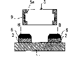
上述实施例1未对金属部件5的电极5a进行预备焊接。实施例2中,对金属部件5的电极5a也进行了预备焊接。这里的电极5a的母材或用于母材上的材料为Cu。In the first embodiment described above, no preliminary welding is performed on the
如图3A所示,用以Sn-Cu为主成分的预备焊剂6(组分中Cu占0.3~5.0重量%,其余部分为Sn,膜厚为3~50μm)进行预备焊接,然后在预备焊剂6的预备焊剂面7上沾上熔融的Sn-Ag-Cu-Bi本焊剂8(组分中,Ag为0.5~5.0重量%,Cu为0.1~2.0重量%,Bi为0~5.0重量%,其余部分为Sn)。同样用Sn-Cu预备焊剂9(组分中Cu占0.3~5.0重量%,其余部分为Sn)对金属部件5的Cu电极5a表面进行预备焊接。As shown in Figure 3A, pre-soldering is carried out with
接着,如图3B所示,将需要安装的金属部件5放置在本焊剂8中,进行软熔处理。Next, as shown in FIG. 3B , the
这种情况如图4所示,不仅与实施例1同样在安装表面2和预备焊剂6间,以及预备焊剂6和本焊剂8间获得了牢固的连接界面J2和J3。而且,以同样的原理在金属部件的电极5a和本焊剂8间形成了牢固的连接界面J4。In this case, as shown in FIG. 4 , firm connection interfaces J2 and J3 are obtained not only between the mounting
实施例3Example 3
上述各实施例中所用的本焊剂8为Sn-Ag-Cu-Bi,也可使用熔点低于预备焊剂6的本焊剂(Sn-Ag系+添加物)、(Sn-Zn系+添加物)、(Sn-Bi系+添加物)、(Sn-In系+添加物)等。The
本焊剂成分为(Sn-Ag系+添加物)时,Ag系为2.0~5.0重量%,添加物为0~5.0重量%,其余部分为Sn。When the present flux component is (Sn—Ag based + additive), the Ag based component is 2.0 to 5.0% by weight, the additive is 0 to 5.0% by weight, and the remainder is Sn.
本焊剂成分为(Sn-Zn系+添加物)时,Zn系为2.0~10.0重量%,添加物为0~5.0重量%,其余部分为Sn。When the flux component is (Sn—Zn based + additive), the Zn based component is 2.0 to 10.0% by weight, the additive is 0 to 5.0% by weight, and the balance is Sn.
本焊剂成分为(Sn-Bi系+添加物)时,Bi系为35.0~60.0重量%,添加物为0~5.0重量%,其余部分为Sn。When the present flux composition is (Sn—Bi system+additive), the Bi system is 35.0 to 60.0% by weight, the additive is 0 to 5.0% by weight, and the balance is Sn.
本焊剂成分为(Sn-In系+添加物)时,In系为40.0~60.0重量%,添加物为0~5.0重量%,其余部分为Sn。When the present flux composition is (Sn-In-based + additive), the In-based content is 40.0 to 60.0% by weight, the additive is 0 to 5.0% by weight, and the balance is Sn.
添加物是由Bi、In、P、Ge、Ga、Ni单独或组合而成的物质。它们的混合比例是,Bi为0~5.0重量%、In为0~5.0重量%、P为0~1.0重量%、Ge为0~1.0重量%、Ga为0~1.0重量%、Ni为0~1.0重量%。Bi是为降低熔点而添加的组分,In是为提高焊接强度及降低熔点而添加的组分,P和Ge是为抑制氧化而添加的组分,Ga是为防止结晶变得粗大而添加的组分,Ni是为改善流动性而添加的组分。The additives are Bi, In, P, Ge, Ga, and Ni alone or in combination. Their mixing ratio is 0 to 5.0% by weight of Bi, 0 to 5.0% by weight of In, 0 to 1.0% by weight of P, 0 to 1.0% by weight of Ge, 0 to 1.0% by weight of Ga, and 0 to 1.0% by weight of Ni. 1.0% by weight. Bi is added to lower the melting point, In is added to increase the welding strength and lower the melting point, P and Ge are added to suppress oxidation, and Ga is added to prevent the crystal from becoming coarse Components, Ni is a component added to improve fluidity.
实施例4Example 4
上述实施例2和实施例3中,用预备焊剂6和9分别对印刷电路板1的安装表面2和金属部件的电极5a进行了预备焊接。也可用预备焊剂9只对金属部件的电极5a进行预备焊接处理。与传统焊接方法相比,该实施例也能够获得连接强度有所提高的效果。In the above-described
如上所述,本发明对金属部件的焊接进行了说明,这种技术同样适用于半导体或电子部件的各种导电片或电极的焊接。As described above, the present invention has been described for the welding of metal parts, and this technique is equally applicable to the welding of various conductive sheets or electrodes of semiconductor or electronic parts.
Claims (3)
Applications Claiming Priority (2)
| Application Number | Priority Date | Filing Date | Title |
|---|---|---|---|
| JP214445/1999 | 1999-07-29 | ||
| JP21444599A JP3514670B2 (en) | 1999-07-29 | 1999-07-29 | Soldering method |
Publications (2)
| Publication Number | Publication Date |
|---|---|
| CN1282643A CN1282643A (en) | 2001-02-07 |
| CN1140373C true CN1140373C (en) | 2004-03-03 |
Family
ID=16655894
Family Applications (1)
| Application Number | Title | Priority Date | Filing Date |
|---|---|---|---|
| CNB00122283XA Expired - Fee Related CN1140373C (en) | 1999-07-29 | 2000-07-28 | Welding method |
Country Status (4)
| Country | Link |
|---|---|
| US (1) | US6334570B1 (en) |
| JP (1) | JP3514670B2 (en) |
| KR (1) | KR100602884B1 (en) |
| CN (1) | CN1140373C (en) |
Families Citing this family (16)
| Publication number | Priority date | Publication date | Assignee | Title |
|---|---|---|---|---|
| JP3312618B2 (en) * | 2000-02-03 | 2002-08-12 | 千住金属工業株式会社 | How to supply additional solder to the solder bath |
| US6896172B2 (en) * | 2000-08-22 | 2005-05-24 | Senju Metal Industry Co., Ltd. | Lead-free solder paste for reflow soldering |
| JP2003198117A (en) | 2001-12-28 | 2003-07-11 | Matsushita Electric Ind Co Ltd | Soldering method and joint structure |
| JP4416373B2 (en) * | 2002-03-08 | 2010-02-17 | 株式会社日立製作所 | Electronics |
| US6933505B2 (en) * | 2002-03-13 | 2005-08-23 | Oy Ajat Ltd | Low temperature, bump-bonded radiation imaging device |
| JP4447215B2 (en) * | 2002-12-16 | 2010-04-07 | Necエレクトロニクス株式会社 | Electronic components |
| US20040155097A1 (en) * | 2003-02-04 | 2004-08-12 | Matsushita Electric Industrial Co., Ltd. | Soldering method and method for manufacturing component mounting board |
| TW591780B (en) * | 2003-03-21 | 2004-06-11 | Univ Nat Central | Flip chip Au bump structure and method of manufacturing the same |
| JP5696173B2 (en) * | 2005-08-12 | 2015-04-08 | アンタヤ・テクノロジーズ・コープ | Solder composition |
| JP2007059506A (en) * | 2005-08-23 | 2007-03-08 | Toppan Printing Co Ltd | Pre-soldered wiring board |
| CN101442174B (en) * | 2008-12-02 | 2010-10-06 | 浙江大学 | Method for Welding Electrical Outer Leads on Electrodes of ITO Conductive Glass |
| JP5339968B2 (en) * | 2009-03-04 | 2013-11-13 | パナソニック株式会社 | Mounting structure and motor |
| CN104203490B (en) * | 2012-03-20 | 2018-04-24 | 阿尔发装配解决方案有限公司 | Solder preform part and solder alloy assembly method |
| JP6489037B2 (en) * | 2016-02-10 | 2019-03-27 | 株式会社デンソー | Electronic device and manufacturing method thereof |
| CN110997223A (en) * | 2017-08-07 | 2020-04-10 | 凯米特电子公司 | Leadless stack comprising a plurality of components |
| CN113000963B (en) * | 2021-03-29 | 2022-07-22 | 杭州凯龙医疗器械有限公司 | Welding method for titanium window of CT tube |
Family Cites Families (11)
| Publication number | Priority date | Publication date | Assignee | Title |
|---|---|---|---|---|
| US3836745A (en) * | 1969-03-13 | 1974-09-17 | Argus Eng Co | Soldering method |
| US4468076A (en) * | 1982-07-23 | 1984-08-28 | Raychem Corporation | Array package connector and connector tool |
| US4758926A (en) * | 1986-03-31 | 1988-07-19 | Microelectronics And Computer Technology Corporation | Fluid-cooled integrated circuit package |
| US4921157A (en) * | 1989-03-15 | 1990-05-01 | Microelectronics Center Of North Carolina | Fluxless soldering process |
| US5374331A (en) * | 1991-10-22 | 1994-12-20 | Argus International | Preflux coating method |
| US5229070A (en) * | 1992-07-02 | 1993-07-20 | Motorola, Inc. | Low temperature-wetting tin-base solder paste |
| US5221038A (en) | 1992-10-05 | 1993-06-22 | Motorola, Inc. | Method for forming tin-indium or tin-bismuth solder connection having increased melting temperature |
| US5463191A (en) * | 1994-03-14 | 1995-10-31 | Dell Usa, L.P. | Circuit board having an improved fine pitch ball grid array and method of assembly therefor |
| US5551627A (en) * | 1994-09-29 | 1996-09-03 | Motorola, Inc. | Alloy solder connect assembly and method of connection |
| EP1134805B1 (en) * | 1995-03-20 | 2004-07-21 | Unitive International Limited | Solder bump fabrication methods and structure including a titanium barrier layer |
| US6076726A (en) * | 1998-07-01 | 2000-06-20 | International Business Machines Corporation | Pad-on-via assembly technique |
-
1999
- 1999-07-29 JP JP21444599A patent/JP3514670B2/en not_active Expired - Fee Related
-
2000
- 2000-07-28 US US09/628,274 patent/US6334570B1/en not_active Expired - Lifetime
- 2000-07-28 KR KR1020000043834A patent/KR100602884B1/en not_active Expired - Fee Related
- 2000-07-28 CN CNB00122283XA patent/CN1140373C/en not_active Expired - Fee Related
Also Published As
| Publication number | Publication date |
|---|---|
| US6334570B1 (en) | 2002-01-01 |
| JP3514670B2 (en) | 2004-03-31 |
| KR100602884B1 (en) | 2006-07-19 |
| KR20010015469A (en) | 2001-02-26 |
| CN1282643A (en) | 2001-02-07 |
| JP2001044615A (en) | 2001-02-16 |
Similar Documents
| Publication | Publication Date | Title |
|---|---|---|
| CN1140373C (en) | Welding method | |
| JP3622788B2 (en) | Lead-free solder alloy | |
| CN1094084C (en) | Soldering tin alloy for electronic part bonding electrodes and soldering method | |
| EP0855242B1 (en) | Lead-free solder | |
| CN101208173B (en) | Lead-free solder paste and its preparation method | |
| CN1267243C (en) | Soldering tin paste | |
| KR100999331B1 (en) | Lead-free solder alloy | |
| JP2002018589A (en) | Lead-free solder alloy | |
| JP3312618B2 (en) | How to supply additional solder to the solder bath | |
| CN1445049A (en) | Soldering tin paste, welding finished product and welding method | |
| TWI695893B (en) | Solder paste | |
| JP3878978B2 (en) | Lead-free solder and lead-free fittings | |
| JPH09277082A (en) | Solder paste | |
| JPH11221694A (en) | Mounting structure using lead-free solder and mounting method using the same | |
| JPH0994687A (en) | Lead-free solder alloy | |
| CN1732063A (en) | Lead-Free Mixed Alloy Solder Paste | |
| CN103596723B (en) | Scaling powder | |
| JPWO2005089999A1 (en) | Lead-free solder balls | |
| JP2005297011A (en) | Solder paste and soldering article | |
| JP2003154486A (en) | Low melting leadless solder less producing dross | |
| JP2004095907A (en) | Solder joint structure and solder paste | |
| JP4544798B2 (en) | Electronic component assembly inspection method, electronic circuit board and electronic equipment manufactured using the method | |
| JP5825265B2 (en) | Soldering method for printed circuit boards | |
| WO2014142153A1 (en) | Solder alloy and joint thereof | |
| KR102343751B1 (en) | Solder paste, soldered joint formed using the same, and flexible printed circuit board having the soldered joint |
Legal Events
| Date | Code | Title | Description |
|---|---|---|---|
| C06 | Publication | ||
| PB01 | Publication | ||
| C10 | Entry into substantive examination | ||
| SE01 | Entry into force of request for substantive examination | ||
| C14 | Grant of patent or utility model | ||
| GR01 | Patent grant | ||
| CF01 | Termination of patent right due to non-payment of annual fee |
Granted publication date: 20040303 Termination date: 20140728 |
|
| EXPY | Termination of patent right or utility model |