CN113614261A - Circuit board, and heat dissipating board or electronic device provided with same - Google Patents
Circuit board, and heat dissipating board or electronic device provided with same Download PDFInfo
- Publication number
- CN113614261A CN113614261A CN202080022980.9A CN202080022980A CN113614261A CN 113614261 A CN113614261 A CN 113614261A CN 202080022980 A CN202080022980 A CN 202080022980A CN 113614261 A CN113614261 A CN 113614261A
- Authority
- CN
- China
- Prior art keywords
- substrate
- aluminum
- bonding layer
- metal layer
- layer
- Prior art date
- Legal status (The legal status is an assumption and is not a legal conclusion. Google has not performed a legal analysis and makes no representation as to the accuracy of the status listed.)
- Pending
Links
- 239000000758 substrate Substances 0.000 claims abstract description 85
- 229910052751 metal Inorganic materials 0.000 claims abstract description 44
- 239000002184 metal Substances 0.000 claims abstract description 44
- 239000000919 ceramic Substances 0.000 claims abstract description 34
- 229910052782 aluminium Inorganic materials 0.000 claims abstract description 33
- XAGFODPZIPBFFR-UHFFFAOYSA-N aluminium Chemical compound [Al] XAGFODPZIPBFFR-UHFFFAOYSA-N 0.000 claims abstract description 33
- XUIMIQQOPSSXEZ-UHFFFAOYSA-N Silicon Chemical compound [Si] XUIMIQQOPSSXEZ-UHFFFAOYSA-N 0.000 claims abstract description 14
- 229910052710 silicon Inorganic materials 0.000 claims abstract description 14
- 239000010703 silicon Substances 0.000 claims abstract description 14
- RYGMFSIKBFXOCR-UHFFFAOYSA-N Copper Chemical compound [Cu] RYGMFSIKBFXOCR-UHFFFAOYSA-N 0.000 claims abstract description 11
- 229910052802 copper Inorganic materials 0.000 claims abstract description 11
- 239000010949 copper Substances 0.000 claims abstract description 11
- QVGXLLKOCUKJST-UHFFFAOYSA-N atomic oxygen Chemical compound [O] QVGXLLKOCUKJST-UHFFFAOYSA-N 0.000 claims abstract description 9
- 239000001301 oxygen Substances 0.000 claims abstract description 9
- 229910052760 oxygen Inorganic materials 0.000 claims abstract description 9
- RTAQQCXQSZGOHL-UHFFFAOYSA-N Titanium Chemical compound [Ti] RTAQQCXQSZGOHL-UHFFFAOYSA-N 0.000 claims description 29
- 229910052719 titanium Inorganic materials 0.000 claims description 29
- 239000010936 titanium Substances 0.000 claims description 29
- 229910000838 Al alloy Inorganic materials 0.000 claims description 13
- YKTSYUJCYHOUJP-UHFFFAOYSA-N [O--].[Al+3].[Al+3].[O-][Si]([O-])([O-])[O-] Chemical compound [O--].[Al+3].[Al+3].[O-][Si]([O-])([O-])[O-] YKTSYUJCYHOUJP-UHFFFAOYSA-N 0.000 claims description 9
- 238000000034 method Methods 0.000 claims description 9
- ZOKXTWBITQBERF-UHFFFAOYSA-N Molybdenum Chemical compound [Mo] ZOKXTWBITQBERF-UHFFFAOYSA-N 0.000 claims description 8
- 229910052750 molybdenum Inorganic materials 0.000 claims description 8
- 239000011733 molybdenum Substances 0.000 claims description 8
- WFKWXMTUELFFGS-UHFFFAOYSA-N tungsten Chemical compound [W] WFKWXMTUELFFGS-UHFFFAOYSA-N 0.000 claims description 7
- 229910052721 tungsten Inorganic materials 0.000 claims description 7
- 239000010937 tungsten Substances 0.000 claims description 7
- 150000004767 nitrides Chemical class 0.000 claims description 6
- 150000004678 hydrides Chemical class 0.000 claims description 5
- -1 oxide Chemical class 0.000 claims description 4
- 238000010438 heat treatment Methods 0.000 description 15
- 229910052581 Si3N4 Inorganic materials 0.000 description 10
- HQVNEWCFYHHQES-UHFFFAOYSA-N silicon nitride Chemical compound N12[Si]34N5[Si]62N3[Si]51N64 HQVNEWCFYHHQES-UHFFFAOYSA-N 0.000 description 10
- 239000002904 solvent Substances 0.000 description 10
- 230000017525 heat dissipation Effects 0.000 description 8
- PMHQVHHXPFUNSP-UHFFFAOYSA-M copper(1+);methylsulfanylmethane;bromide Chemical compound Br[Cu].CSC PMHQVHHXPFUNSP-UHFFFAOYSA-M 0.000 description 7
- 238000005211 surface analysis Methods 0.000 description 7
- IJGRMHOSHXDMSA-UHFFFAOYSA-N Atomic nitrogen Chemical compound N#N IJGRMHOSHXDMSA-UHFFFAOYSA-N 0.000 description 6
- 239000011248 coating agent Substances 0.000 description 6
- 238000000576 coating method Methods 0.000 description 6
- PNEYBMLMFCGWSK-UHFFFAOYSA-N Alumina Chemical compound [O-2].[O-2].[O-2].[Al+3].[Al+3] PNEYBMLMFCGWSK-UHFFFAOYSA-N 0.000 description 5
- KPUWHANPEXNPJT-UHFFFAOYSA-N disiloxane Chemical class [SiH3]O[SiH3] KPUWHANPEXNPJT-UHFFFAOYSA-N 0.000 description 5
- 238000009616 inductively coupled plasma Methods 0.000 description 5
- NRTOMJZYCJJWKI-UHFFFAOYSA-N Titanium nitride Chemical compound [Ti]#N NRTOMJZYCJJWKI-UHFFFAOYSA-N 0.000 description 4
- 238000002441 X-ray diffraction Methods 0.000 description 4
- 238000007639 printing Methods 0.000 description 4
- 238000007650 screen-printing Methods 0.000 description 4
- GWEVSGVZZGPLCZ-UHFFFAOYSA-N Titan oxide Chemical compound O=[Ti]=O GWEVSGVZZGPLCZ-UHFFFAOYSA-N 0.000 description 3
- 150000004703 alkoxides Chemical class 0.000 description 3
- 239000012298 atmosphere Substances 0.000 description 3
- 230000015572 biosynthetic process Effects 0.000 description 3
- 239000013522 chelant Substances 0.000 description 3
- 238000001816 cooling Methods 0.000 description 3
- 238000002149 energy-dispersive X-ray emission spectroscopy Methods 0.000 description 3
- 238000007733 ion plating Methods 0.000 description 3
- 230000007774 longterm Effects 0.000 description 3
- 229910052757 nitrogen Inorganic materials 0.000 description 3
- 239000012299 nitrogen atmosphere Substances 0.000 description 3
- 239000004065 semiconductor Substances 0.000 description 3
- 238000004544 sputter deposition Methods 0.000 description 3
- 229910000048 titanium hydride Inorganic materials 0.000 description 3
- OGIDPMRJRNCKJF-UHFFFAOYSA-N titanium oxide Inorganic materials [Ti]=O OGIDPMRJRNCKJF-UHFFFAOYSA-N 0.000 description 3
- MTPVUVINMAGMJL-UHFFFAOYSA-N trimethyl(1,1,2,2,2-pentafluoroethyl)silane Chemical compound C[Si](C)(C)C(F)(F)C(F)(F)F MTPVUVINMAGMJL-UHFFFAOYSA-N 0.000 description 3
- 238000007740 vapor deposition Methods 0.000 description 3
- OKTJSMMVPCPJKN-UHFFFAOYSA-N Carbon Chemical compound [C] OKTJSMMVPCPJKN-UHFFFAOYSA-N 0.000 description 2
- 229910002808 Si–O–Si Inorganic materials 0.000 description 2
- 229910052799 carbon Inorganic materials 0.000 description 2
- 150000001875 compounds Chemical class 0.000 description 2
- 239000000470 constituent Substances 0.000 description 2
- 238000009792 diffusion process Methods 0.000 description 2
- 239000011261 inert gas Substances 0.000 description 2
- 239000000463 material Substances 0.000 description 2
- 229910044991 metal oxide Inorganic materials 0.000 description 2
- 150000004706 metal oxides Chemical class 0.000 description 2
- 239000011224 oxide ceramic Substances 0.000 description 2
- 229910052574 oxide ceramic Inorganic materials 0.000 description 2
- TWNQGVIAIRXVLR-UHFFFAOYSA-N oxo(oxoalumanyloxy)alumane Chemical compound O=[Al]O[Al]=O TWNQGVIAIRXVLR-UHFFFAOYSA-N 0.000 description 2
- 239000000843 powder Substances 0.000 description 2
- 229910021332 silicide Inorganic materials 0.000 description 2
- FVBUAEGBCNSCDD-UHFFFAOYSA-N silicide(4-) Chemical compound [Si-4] FVBUAEGBCNSCDD-UHFFFAOYSA-N 0.000 description 2
- 238000005507 spraying Methods 0.000 description 2
- UFHFLCQGNIYNRP-UHFFFAOYSA-N Hydrogen Chemical compound [H][H] UFHFLCQGNIYNRP-UHFFFAOYSA-N 0.000 description 1
- 230000004888 barrier function Effects 0.000 description 1
- 238000005219 brazing Methods 0.000 description 1
- 230000000295 complement effect Effects 0.000 description 1
- 238000012790 confirmation Methods 0.000 description 1
- 239000002826 coolant Substances 0.000 description 1
- 239000012809 cooling fluid Substances 0.000 description 1
- 238000005336 cracking Methods 0.000 description 1
- 230000000694 effects Effects 0.000 description 1
- 238000000921 elemental analysis Methods 0.000 description 1
- 238000004993 emission spectroscopy Methods 0.000 description 1
- 230000005669 field effect Effects 0.000 description 1
- 238000010304 firing Methods 0.000 description 1
- 239000001257 hydrogen Substances 0.000 description 1
- 229910052739 hydrogen Inorganic materials 0.000 description 1
- 238000010030 laminating Methods 0.000 description 1
- 238000004519 manufacturing process Methods 0.000 description 1
- 238000005259 measurement Methods 0.000 description 1
- 238000002156 mixing Methods 0.000 description 1
- 239000000203 mixture Substances 0.000 description 1
- RVTZCBVAJQQJTK-UHFFFAOYSA-N oxygen(2-);zirconium(4+) Chemical compound [O-2].[O-2].[Zr+4] RVTZCBVAJQQJTK-UHFFFAOYSA-N 0.000 description 1
- 238000003825 pressing Methods 0.000 description 1
- 238000004445 quantitative analysis Methods 0.000 description 1
- 239000002994 raw material Substances 0.000 description 1
- 239000003507 refrigerant Substances 0.000 description 1
- 239000000523 sample Substances 0.000 description 1
- 238000001004 secondary ion mass spectrometry Methods 0.000 description 1
- HBMJWWWQQXIZIP-UHFFFAOYSA-N silicon carbide Chemical compound [Si+]#[C-] HBMJWWWQQXIZIP-UHFFFAOYSA-N 0.000 description 1
- 229910010271 silicon carbide Inorganic materials 0.000 description 1
- 229910052709 silver Inorganic materials 0.000 description 1
- 239000004332 silver Substances 0.000 description 1
- 238000000859 sublimation Methods 0.000 description 1
- 230000008022 sublimation Effects 0.000 description 1
- 150000003658 tungsten compounds Chemical class 0.000 description 1
- 238000004846 x-ray emission Methods 0.000 description 1
- 229910001928 zirconium oxide Inorganic materials 0.000 description 1
Images


Classifications
-
- H—ELECTRICITY
- H01—ELECTRIC ELEMENTS
- H01L—SEMICONDUCTOR DEVICES NOT COVERED BY CLASS H10
- H01L23/00—Details of semiconductor or other solid state devices
- H01L23/12—Mountings, e.g. non-detachable insulating substrates
- H01L23/14—Mountings, e.g. non-detachable insulating substrates characterised by the material or its electrical properties
- H01L23/142—Metallic substrates having insulating layers
-
- H—ELECTRICITY
- H01—ELECTRIC ELEMENTS
- H01L—SEMICONDUCTOR DEVICES NOT COVERED BY CLASS H10
- H01L23/00—Details of semiconductor or other solid state devices
- H01L23/34—Arrangements for cooling, heating, ventilating or temperature compensation ; Temperature sensing arrangements
- H01L23/36—Selection of materials, or shaping, to facilitate cooling or heating, e.g. heatsinks
- H01L23/373—Cooling facilitated by selection of materials for the device or materials for thermal expansion adaptation, e.g. carbon
- H01L23/3735—Laminates or multilayers, e.g. direct bond copper ceramic substrates
-
- B—PERFORMING OPERATIONS; TRANSPORTING
- B23—MACHINE TOOLS; METAL-WORKING NOT OTHERWISE PROVIDED FOR
- B23K—SOLDERING OR UNSOLDERING; WELDING; CLADDING OR PLATING BY SOLDERING OR WELDING; CUTTING BY APPLYING HEAT LOCALLY, e.g. FLAME CUTTING; WORKING BY LASER BEAM
- B23K35/00—Rods, electrodes, materials, or media, for use in soldering, welding, or cutting
- B23K35/22—Rods, electrodes, materials, or media, for use in soldering, welding, or cutting characterised by the composition or nature of the material
- B23K35/24—Selection of soldering or welding materials proper
- B23K35/28—Selection of soldering or welding materials proper with the principal constituent melting at less than 950 degrees C
-
- C—CHEMISTRY; METALLURGY
- C04—CEMENTS; CONCRETE; ARTIFICIAL STONE; CERAMICS; REFRACTORIES
- C04B—LIME, MAGNESIA; SLAG; CEMENTS; COMPOSITIONS THEREOF, e.g. MORTARS, CONCRETE OR LIKE BUILDING MATERIALS; ARTIFICIAL STONE; CERAMICS; REFRACTORIES; TREATMENT OF NATURAL STONE
- C04B37/00—Joining burned ceramic articles with other burned ceramic articles or other articles by heating
- C04B37/02—Joining burned ceramic articles with other burned ceramic articles or other articles by heating with metallic articles
-
- C—CHEMISTRY; METALLURGY
- C22—METALLURGY; FERROUS OR NON-FERROUS ALLOYS; TREATMENT OF ALLOYS OR NON-FERROUS METALS
- C22C—ALLOYS
- C22C21/00—Alloys based on aluminium
-
- H—ELECTRICITY
- H01—ELECTRIC ELEMENTS
- H01L—SEMICONDUCTOR DEVICES NOT COVERED BY CLASS H10
- H01L23/00—Details of semiconductor or other solid state devices
- H01L23/34—Arrangements for cooling, heating, ventilating or temperature compensation ; Temperature sensing arrangements
- H01L23/36—Selection of materials, or shaping, to facilitate cooling or heating, e.g. heatsinks
- H01L23/373—Cooling facilitated by selection of materials for the device or materials for thermal expansion adaptation, e.g. carbon
- H01L23/3731—Ceramic materials or glass
-
- H—ELECTRICITY
- H05—ELECTRIC TECHNIQUES NOT OTHERWISE PROVIDED FOR
- H05K—PRINTED CIRCUITS; CASINGS OR CONSTRUCTIONAL DETAILS OF ELECTRIC APPARATUS; MANUFACTURE OF ASSEMBLAGES OF ELECTRICAL COMPONENTS
- H05K1/00—Printed circuits
- H05K1/02—Details
-
- H—ELECTRICITY
- H01—ELECTRIC ELEMENTS
- H01L—SEMICONDUCTOR DEVICES NOT COVERED BY CLASS H10
- H01L23/00—Details of semiconductor or other solid state devices
- H01L23/12—Mountings, e.g. non-detachable insulating substrates
- H01L23/14—Mountings, e.g. non-detachable insulating substrates characterised by the material or its electrical properties
- H01L23/15—Ceramic or glass substrates
Abstract
A circuit board of the present invention includes: a substrate formed of a ceramic, a bonding layer located over the substrate, and a metal layer located over the bonding layer. In addition, the metal layer contains copper. In addition, the bonding layer contains aluminum, silicon, and oxygen.
Description
Technical Field
The present invention relates to a circuit board, and a heat dissipating board or an electronic device provided with the circuit board.
Background
An electronic device is known in which a circuit substrate is provided with a metal layer, and various electronic components such as a semiconductor element, a heat generating element, and a peltier element are mounted on the metal layer. A circuit substrate used in such applications includes a substrate and a metal layer formed of copper having excellent heat dissipation properties and located on the substrate.
Here, a ceramic having both excellent insulating properties and mechanical strength is used as the substrate. As a bonding layer for bonding the substrate and the metal layer, for example, a brazing material containing silver and copper as main components is used (for example, see patent document 1).
Documents of the prior art
Patent document
Patent document 1: japanese laid-open patent publication No. 2012-115846
Disclosure of Invention
A circuit board of the present invention includes: a substrate formed of a ceramic, a bonding layer located over the substrate, and a metal layer located over the bonding layer. In addition, the metal layer contains copper. In addition, the bonding layer contains aluminum, silicon, and oxygen.
Effects of the invention
The circuit board of the present invention is resistant to cracking of the bonding layer even when repeatedly heated and cooled, and can withstand long-term use.
Drawings
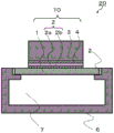
Fig. 1 is a cross-sectional view schematically showing a circuit substrate according to embodiment 1 of the present invention.
Fig. 2 is a cross-sectional view schematically showing a circuit substrate according to embodiment 2 of the present invention.
Fig. 3 is a cross-sectional view schematically showing a circuit substrate according to embodiment 3 of the present invention.
Fig. 4 is a cross-sectional view schematically showing a circuit substrate according to embodiment 4 of the present invention.
Fig. 5 is a cross-sectional view schematically showing a circuit substrate according to embodiment 5 of the present invention.
Fig. 6 is a sectional view schematically showing a heat-dissipating substrate of the present invention.
Detailed Description
Hereinafter, the circuit board of the present invention will be described in detail with reference to the drawings.
As shown in fig. 1, a circuit board 10 according to embodiment 1 of the present invention includes: a substrate 1, a bonding layer 2 located over the substrate 1, and a metal layer 3 located over the bonding layer 2.
Here, the substrate 1 is formed of ceramic. As the ceramic, for example, a ceramic containing aluminum or silicon such as a silicon carbide ceramic, an aluminum oxide ceramic containing zirconium oxide, a silicon nitride ceramic, or an aluminum nitride ceramic can be used.
When the substrate 1 is formed of a nitride-based ceramic such as a silicon nitride ceramic, an aluminum oxide ceramic, or an aluminum nitride ceramic, the heat dissipation performance of the circuit substrate 10 of embodiment 1 can be improved because of high thermal conductivity. The silicon nitride ceramic is a ceramic in which silicon nitride accounts for 70 mass% or more of 100 mass% of the total components constituting the silicon nitride ceramic. The alumina ceramic is a ceramic in which alumina accounts for 70 mass% of the total components constituting the alumina ceramic. The aluminum nitride ceramic is a ceramic in which aluminum nitride accounts for 70 mass% or more of the total components constituting the aluminum nitride ceramic.
The material of the substrate 1 can be confirmed by the following method. First, measurement is performed using an X-ray diffraction apparatus (XRD), and the obtained value of 2 θ (2 θ is a diffraction angle.) is determined using a JCPDS card, thereby determining the constituent components of the target substrate. Next, quantitative analysis of the target substrate was performed using an ICP (inductively Coupled plasma) emission spectrometry apparatus (ICP). At this time, if the constituent component determined by XRD is silicon nitride, and the content of silicon (Si) measured by ICP is converted to silicon nitride (Si)3N4) If the value of (b) is 70% by mass or more, the ceramic is a silicon nitride ceramic. The same applies to other ceramics.
The metal layer 3 in the circuit board 10 according to embodiment 1 of the present invention contains copper. Since the metal layer 3 contains copper having high thermal conductivity, the circuit board 10 according to embodiment 1 of the present invention has excellent heat dissipation properties. The metal layer 3 may contain, for example, 90 mass% or more of copper out of 100 mass% of the total components. Since most of the metal layer 3 is made of copper having high thermal conductivity, the circuit board 10 according to embodiment 1 of the present invention has excellent heat dissipation properties.
The average thickness of the metal layer 3 may be, for example, 100 μm or more and 3000 μm or less.
In addition, bonding layer 2 in circuit board 10 according to embodiment 1 of the present invention contains aluminum, silicon, and oxygen. In the bonding layer 2, the total of aluminum, silicon, and oxygen may be 95 mass% or more, for example, out of 100 mass% of the total components constituting the layer.
Specifically, the bonding layer 2 may be formed such that aluminum is 70 mass% or more and 85 mass% or less, silicon is 4 mass% or more and 15 mass% or less, and oxygen is 5 mass% or more and 15 mass% or less, out of 100 mass% of the total components constituting the bonding layer 2.
By satisfying such a configuration, the substrate 1 made of ceramic and the metal layer 3 containing copper can be firmly bonded via the bonding layer 2.
In addition, as shown in fig. 2, the bonding layer 2 in the circuit substrate 10 of embodiment 2 of the present invention may have a 1 st region 2a and a 2 nd region 2 b.
The 1 st region 2a is mainly connected to the metal layer 3, and the 2 nd region 2b is connected to the substrate 1.
The 1 st region 2a has aluminum or an aluminum alloy. The aluminum alloy has silicon.
The 2 nd region 2b may have aluminum silicate. The aluminum silicate has high affinity with aluminum or aluminum alloy. Therefore, the 1 st region 2a and the 2 nd region 2b are easily and firmly joined.
The 2 nd region 2b may have a sialon. Sialon has high affinity with aluminum or aluminum alloys. Therefore, the 1 st region 2a and the 2 nd region 2b are easily and firmly joined.
In addition, when the 2 nd region 2b has aluminum silicate or sialon, the affinity with aluminum or silicon of the substrate 1 is high. Therefore, the 2 nd region and the substrate are easily firmly bonded. Therefore, the substrate 1 and the bonding layer 2 are easily and firmly bonded.
In addition, when the 2 nd region 2b is aluminum silicate, the affinity with the substrate 1 made of alumina ceramics is high. Therefore, the 2 nd region and the substrate are easily firmly bonded. Therefore, the substrate 1 and the bonding layer 2 are easily and firmly bonded.
In addition, when the 2 nd region 2b is sialon, the affinity with the substrate 1 made of silicon nitride ceramics or aluminum nitride ceramics is high. Therefore, the 2 nd region and the substrate are easily firmly bonded. Therefore, the substrate 1 and the bonding layer 2 are easily and firmly bonded.
Since the substrate 1 and the bonding layer 2 are firmly bonded, the substrate 1 and the metal layer 3 are firmly bonded. Therefore, even if heating and cooling are repeated, the bonding layer 2 is less likely to have cracks. Thus, the circuit board 10 according to embodiment 2 of the present invention can withstand long-term use.
In embodiment 3, as shown in the circuit board 10 of fig. 3, the 2 nd region 2b of the bonding layer 2 may be a layer sandwiched between the 2 nd region 2a and the substrate 1.
The average thickness of the bonding layer 2 may be, for example, 5 μm or more and 40 μm or less.
Here, the components and contents of the bonding layer 2 and the metal layer 3 can be confirmed by the following method. First, the circuit substrate 10 according to embodiment 2 or 3 of the present invention is cut so as to have a cross-sectional shape shown in fig. 2 or 3, and polished by a cross-sectional polisher (CP), thereby obtaining a polished surface. Next, the components constituting the bonding layer 2 and the metal layer 3, respectively, and the contents thereof may be measured using an energy dispersive X-ray analysis (EDS) apparatus provided with a Scanning Electron Microscope (SEM) with the polished surface as an observation surface. Alternatively, the bonding layer 2 and the metal layer 3 may be scraped off, and the components constituting the bonding layer 2 and the metal layer 3, respectively, and the contents thereof may be measured using ICP or fluorescent X-ray analysis (XRF).
In addition, as a method for confirming that the 2 nd region 2b of the bonding layer 2 is sialon or aluminum silicate, when elemental analysis is performed, aluminum and silicon coexist, it is considered to have aluminum silicate, and when silicon, aluminum, oxygen, and nitrogen coexist, it is considered to have sialon.
As shown in fig. 4, circuit board 10 according to embodiment 4 of the present invention includes intermediate layer 4 between bonding layer 2 and metal layer 3, and intermediate layer 4 may contain titanium, tungsten, or molybdenum.
The intermediate layer 4 easily suppresses diffusion of aluminum in the 1 st region 2a of the bonding layer 2 into the metal layer 3. In addition, the strength of the bonding layer 2 can be maintained. Further, the substrate 1 and the metal layer 3 can be further firmly bonded by the affinity of the aluminum alloy in the 1 st region 2a of the bonding layer 2 and the intermediate layer 4. Therefore, even if heating and cooling are repeated, the bonding layer 2 is less likely to have cracks.
The intermediate layer 4 may be formed, for example, such that the total of titanium, tungsten, and molybdenum is 50 mass% or more, based on 100 mass% of the total composition.
The average thickness of the intermediate layer 4 may be, for example, 0.5 μm or more and 5 μm or less.
In the confirmation of the presence of the intermediate layer 4, the polished surface may be used as an observation surface, and an Electron Probe Microanalyzer (EPMA) may be used to perform surface analysis, and the presence or absence of a layer of titanium, tungsten or molybdenum may be determined in a color map of the surface analysis. The content of the component constituting the intermediate layer 4 may be measured by using EDS provided with an SEM with the polished surface as an observation surface.
In addition, titanium contained in the intermediate layer 4 in the circuit substrate 10 according to embodiment 4 of the present invention may exist as a hydride, an oxide, a nitride, a carbide, or a carbonitride. If such a configuration is satisfied, even if heating and cooling are repeated, diffusion of aluminum in the 1 st region 2a of the bonding layer 2 into the metal layer 3 can be further suppressed, and the strength of the bonding layer 2 can be further maintained. Further, the substrate 1 and the metal layer 3 can be further firmly bonded by the affinity between the aluminum alloy in the 1 st region 2a of the bonding layer 2 and the intermediate layer 4, and thus the bonding layer 2 is less likely to crack even if repeatedly heated and cooled.
The intermediate layer 4 may contain, for example, 50 mass% or more of titanium out of 100 mass% of the total components.
The presence or absence of a hydride, an oxide, a nitride, a carbide, or a carbonitride in titanium contained in the intermediate layer 4 can be confirmed by the following method. First, the polished surface was used as an observation surface, and surface analysis was performed by using EPMA. Then, in the color map of the surface analysis, when a site where both titanium and oxygen exist is confirmed, it is considered that an oxide exists. In the color map of the surface analysis, when a site where titanium and nitrogen are present simultaneously is confirmed, it is considered that nitride is present. In addition, in the color map of the surface analysis, when a portion where titanium and carbon are present simultaneously is confirmed, carbide is considered to be present. In the color map of the surface analysis, if a site where titanium, carbon, and nitrogen were present at the same time was confirmed, it was considered that carbonitride was present. As a method for confirming the hydride, the intermediate layer may be cut out and the presence of the hydride may be confirmed by Secondary Ion Mass Spectrometry (SIMS).
As shown in fig. 5, the circuit board 10 of the present invention may have a fin 5 on the base 1.
Further, the fin 5 may be provided on the substrate 1 on the opposite side to the bonding layer 2.
The fins 5 may be made of aluminum, for example. Since the fins 5 are made of aluminum having high thermal conductivity, the heat dissipation performance can be further improved by providing the fins 5.
In the circuit substrate 10 of the present invention, as shown in fig. 5, the bonding layer 2 may be located between the substrate 1 and the fin 5.
In addition, as shown in fig. 2 or fig. 3, the bonding layer 2 of the circuit substrate 10 of the present invention may have a 1 st region 2a and a 2 nd region 2 b.
In the circuit board 10 of the present invention, the substrate 1 may have a flow path therein. If such a configuration is satisfied, the electronic component on the metal layer 3 can be efficiently cooled by flowing a cooling fluid (hereinafter, referred to as a coolant) through the flow path. The flow path may have any shape and size.
As shown in fig. 6, the heat dissipating substrate 20 of the present invention includes the circuit board 10 and the member 6 to form the flow path 7. Here, the member 6 is formed of aluminum or an aluminum alloy. Since the heat dissipation member 20 of the present invention satisfies the above-described configuration, it is lighter in weight and has excellent heat dissipation properties as compared to the case where the member is made of ceramic or the like, and therefore, the electronic component on the metal layer 3 can be efficiently cooled by flowing the refrigerant through the flow path 7.
In the heat dissipating substrate 20 of the present invention, as shown in fig. 6, the bonding layer 2 may be located between the substrate 1 and the member 5 of the circuit substrate 10. If such a constitution is satisfied, the substrate 1 formed of ceramic and the member 5 formed of aluminum or an aluminum alloy are firmly joined, and the heat dissipating substrate 20 of the present invention is suitable for long-term use.
The electronic device of the present invention further includes an electronic component located on the metal layer 3 in the circuit board 10. Alternatively, the electronic component is provided on the metal layer 3 in the circuit board 10 of the heat dissipating substrate 20. By satisfying such a configuration, the electronic device of the present invention can be used for a long period of time and is excellent in reliability.
Here, as the electronic components, for example, a Light Emitting Diode (LED) element, a Laser Diode (LD) element, an Insulated Gate Bipolar Transistor (IGBT) element, an Intelligent Power Module (IPM) element, a metal oxide film type field effect transistor (MOSFET) element, a Free Wheeling Diode (FWD) element, a power transistor (GTR) element, a Schottky Barrier Diode (SBD), a High Electron Mobility Transistor (HEMT) element, a semiconductor element such as a complementary metal oxide film semiconductor (CMOS), a heat generating element for a sublimation type thermal print head or a thermal ink jet print head, a peltier element, or the like can be used.
An example of the method for manufacturing a circuit board according to the present invention will be described below.
First, a substrate made of ceramic is prepared by a known method. Specifically, the substrate can be produced by pressing or laminating ceramic raw materials into a band shape to produce a molded body, and then firing the molded body. The substrate may have a flow path therein.
Next, a metal layer containing 90 mass% or more of copper is prepared. Here, in order to interpose the intermediate layer containing titanium, tungsten, or molybdenum between the bonding layer and the metal layer, which will be described later, a solvent of a titanium, molybdenum, or tungsten-containing compound, which is an alkoxide system or chelate system, is applied to the metal layer by screen printing, brush coating, inkjet coating, bar coating, spray coating, or the like, and the intermediate layer is previously formed on the metal layer by heat treatment at a temperature of 150 ℃ to 650 ℃ for 15 minutes or more. Here, when screen printing is used, the intermediate layer can be easily formed to have an arbitrary thickness. Further, by using such a solvent containing a titanium, molybdenum or tungsten compound as an alkoxide or chelate, even if the area of the intermediate layer is large, a film can be formed uniformly and quickly. The intermediate layer may be formed by sputtering, vapor deposition, ion plating, film formation, or the like.
In order to make the intermediate layer contain titanium hydride, titanium oxide, titanium nitride, titanium carbide, or titanium carbonitride, the following method can be used.
In the case of titanium hydride, a titanium-containing layer is formed by sputtering, vapor deposition, ion plating, film formation, or printing a titanium-containing solvent, and then heat treatment is performed at 550 ℃ or lower in a hydrogen atmosphere.
In the case of titanium oxide, a titanium-containing solvent is printed to form a titanium-containing layer, and then heat treatment is performed at 500 ℃ to 650 ℃ in an inert gas atmosphere.
In the case of titanium nitride, a titanium-containing layer is formed by sputtering, vapor deposition, ion plating, film formation, or printing a titanium-containing solvent, and then heat treatment is performed at 500 ℃ to 650 ℃ in a nitrogen atmosphere.
In the case of titanium carbonitride, after a titanium-containing layer is formed by printing a titanium-containing solvent, heat treatment is performed at 500 ℃ to 650 ℃ in a nitrogen atmosphere.
In the case of titanium carbide, a titanium-containing layer is formed by printing a titanium-containing solvent, and then heat treatment is performed at 500 ℃ to 650 ℃ in an inert gas atmosphere or a nitrogen atmosphere.
As the "titanium-containing solvent", an alkoxide-based solvent, a chelate-based solvent, or the like can be used.
Next, a paste containing siloxane and aluminum to be a bonding layer was prepared. Here, the mixing ratio of siloxane and aluminum may be 95 mass% or more of the total of aluminum, silicon, and oxygen among 100 mass% of the total components constituting the bonding layer after the heat treatment at the time of bonding described later.
In addition, a flaky powder may be used as the aluminum. By using such a powder, aluminum diffuses in a wide range, and therefore the bonding layer can be formed efficiently. In particular, the 2 nd region 2b is easily formed.
The thickness of the scale-like aluminum may be, for example, 1 μm or more and 5 μm or less.
The outer diameter of the scale-like aluminum may be, for example, 10 μm or more and 20 μm or less.
Next, a paste to be a bonding layer is applied to one of the surfaces of the substrate or the metal layer (the intermediate layer in the case where the metal layer has the intermediate layer) to be bonded, using screen printing, brush coating, inkjet coating, bar coating, spray coating, or the like. Here, when screen printing is used, the bonding layer can be easily formed to have an arbitrary thickness.
Then, at 1 × 10⁻¹The heat treatment is carried out at a temperature of 560 ℃ to 700 ℃ in a vacuum of Pa or less for 15 minutes or more. By this heat treatment, Si-O-Si groups in the siloxane are reacted with aluminum to form an aluminum alloy. When Si-O-Si groups in siloxane react with aluminum, the surface side of the substrate is decomposed to form compounds such as aluminum silicate and sialon. For example, in the case where the substrate is an alumina ceramic, aluminum silicate is formed. When the substrate is a nitride-based ceramic such as an aluminum nitride ceramic or a silicon nitride ceramic, a sialon is formed. Thus, a silicide or sialon is formedThe bonding layer of (1). The silicide or the sialon has high affinity with aluminum and silicon of the substrate. Therefore, the bonding layer can firmly bond the substrate and the metal layer. Thus, the circuit board of the present invention was obtained.
In addition, if the intermediate layer has titanium nitride, the Si — O — Si group in the siloxane reacts with aluminum by heat treatment, and the resulting aluminum alloy-containing solution has good wettability with the titanium nitride, so that voids are not generated and stronger bonding is possible.
In addition, the intermediate layer may have titanium, tungsten, molybdenum, titanium hydride, titanium oxide, titanium carbide.
Further, a member made of aluminum or an aluminum alloy and having a concave portion is prepared, and before the paste to be the bonding layer is subjected to heat treatment, the paste to be the bonding layer is disposed between the substrate and the member so as to form a flow path through the substrate and the member, and then heat treatment is performed under the above-described conditions, thereby obtaining the heat dissipating substrate of the present invention.
Then, an electronic component is mounted on the metal layer of the circuit board or the heat dissipating board, thereby obtaining the electronic device of the present invention.
Description of the symbols
1: substrate
2: bonding layer
2 a: region 1
2 b: region 2
3: metal layer
4: intermediate layer
5: fin
6: component
7: flow path
10: circuit substrate
20: heat dissipation substrate
Claims (9)
1. A circuit board includes:
a substrate formed of a ceramic,
A bonding layer over the substrate, and
a metal layer located over the bonding layer,
the metal layer contains copper and is formed by a process,
the bonding layer contains aluminum, silicon, and oxygen.
2. The circuit substrate of claim 1,
the bonding layer is provided with a 1 st region and a 2 nd region,
the 1 st region has at least one of aluminum or an aluminum alloy and the 2 nd region is sialon or aluminum silicate.
3. The circuit substrate according to claim 1 or claim 2, wherein an intermediate layer is provided between the bonding layer and the metal layer,
the intermediate layer contains titanium, tungsten or molybdenum.
4. A circuit substrate according to any one of claims 1 to 3, wherein the titanium is present as a hydride, oxide, nitride, carbide or carbonitride.
5. The circuit substrate according to any one of claims 1 to 4, wherein the substrate is provided with a flow path inside.
6. A heat dissipating substrate in which a flow path is formed by the circuit substrate according to any one of claims 1 to 4 and a member formed of aluminum or an aluminum alloy.
7. The heat dissipating substrate according to claim 6, wherein the bonding layer is located between the member and a substrate of the circuit substrate according to any one of claims 1 to 4.
8. An electronic device provided with an electronic component located over the metal layer in the circuit substrate defined in any one of claims 1 to 5.
9. An electronic apparatus provided with an electronic component located over the metal layer in the circuit substrate of the heat dissipating substrate of claim 6 or claim 7.
Applications Claiming Priority (3)
| Application Number | Priority Date | Filing Date | Title |
|---|---|---|---|
| JP2019-056841 | 2019-03-25 | ||
| JP2019056841 | 2019-03-25 | ||
| PCT/JP2020/013039 WO2020196528A1 (en) | 2019-03-25 | 2020-03-24 | Circuit substrate and heat dissipation substrate or electronic device provided with same |
Publications (1)
| Publication Number | Publication Date |
|---|---|
| CN113614261A true CN113614261A (en) | 2021-11-05 |
Family
ID=72608480
Family Applications (1)
| Application Number | Title | Priority Date | Filing Date |
|---|---|---|---|
| CN202080022980.9A Pending CN113614261A (en) | 2019-03-25 | 2020-03-24 | Circuit board, and heat dissipating board or electronic device provided with same |
Country Status (4)
| Country | Link |
|---|---|
| US (1) | US20220189837A1 (en) |
| JP (1) | JP7122461B2 (en) |
| CN (1) | CN113614261A (en) |
| WO (1) | WO2020196528A1 (en) |
Families Citing this family (1)
| Publication number | Priority date | Publication date | Assignee | Title |
|---|---|---|---|---|
| CN116888424A (en) * | 2021-02-26 | 2023-10-13 | 京瓷株式会社 | Thermal device |
Citations (15)
| Publication number | Priority date | Publication date | Assignee | Title |
|---|---|---|---|---|
| US6107638A (en) * | 1997-03-14 | 2000-08-22 | Kabushiki Kaisha Toshiba | Silicon nitride circuit substrate and semiconductor device containing same |
| CN101308783A (en) * | 2007-05-18 | 2008-11-19 | 株式会社半导体能源研究所 | Semiconductor substrate, semiconductor device and manufacturing method thereof |
| WO2011111989A2 (en) * | 2010-03-09 | 2011-09-15 | 주식회사 케이씨씨 | Metal-bonded ceramic substrate |
| CN102593009A (en) * | 2011-01-11 | 2012-07-18 | 三菱综合材料株式会社 | Method for producing substrate for power module, substrate for power module and power module |
| CN103282546A (en) * | 2010-11-19 | 2013-09-04 | 日本发条株式会社 | Laminate and method for producing laminate |
| CN103648766A (en) * | 2011-07-11 | 2014-03-19 | 日本发条株式会社 | Layered body and manufacturing method for layered body |
| CN104067386A (en) * | 2012-02-01 | 2014-09-24 | 三菱综合材料株式会社 | Substrate for power modules, substrate with heat sink for power modules, power module, method for producing substrate for power modules, and paste for bonding copper member |
| CN104205325A (en) * | 2012-03-30 | 2014-12-10 | 三菱综合材料株式会社 | Power module substrate with heat sink, power module substrate with cooler, and power module |
| CN105189109A (en) * | 2013-03-14 | 2015-12-23 | 三菱综合材料株式会社 | Bonded body, substrate for power modules, and substrate with heat sink for power modules |
| CN106663663A (en) * | 2014-08-26 | 2017-05-10 | 三菱综合材料株式会社 | Joined body, substrate for power module provided with heat sink, heat sink, method for manufacturing joined body, method for manufacturing substrate for power module provided with heat sink, and method for manufacturing heat sink |
| JP2017135197A (en) * | 2016-01-26 | 2017-08-03 | 京セラ株式会社 | Circuit board |
| CN107112298A (en) * | 2014-10-16 | 2017-08-29 | 三菱综合材料株式会社 | The power module substrate and its manufacture method of subsidiary cooler |
| CN108292632A (en) * | 2015-11-26 | 2018-07-17 | 三菱综合材料株式会社 | Ceramics-aluminium conjugant, insulate electrical substrate, power module, LED module, electrothermal module |
| CN108682659A (en) * | 2018-05-16 | 2018-10-19 | 江苏芯澄半导体有限公司 | A kind of wide bandgap semiconductor silicon carbide power device encapsulating structure for new-energy automobile |
| CN109417056A (en) * | 2016-06-30 | 2019-03-01 | 三菱综合材料株式会社 | Copper-ceramic joined article and insulate electrical substrate |
Family Cites Families (4)
| Publication number | Priority date | Publication date | Assignee | Title |
|---|---|---|---|---|
| JP3907818B2 (en) * | 1997-03-14 | 2007-04-18 | 株式会社東芝 | Silicon nitride circuit board, semiconductor device, and method of manufacturing silicon nitride circuit board |
| US6528123B1 (en) * | 2000-06-28 | 2003-03-04 | Sandia Corporation | Coating system to permit direct brazing of ceramics |
| JP5423076B2 (en) * | 2008-06-06 | 2014-02-19 | 三菱マテリアル株式会社 | Power module substrate, power module, and method of manufacturing power module substrate |
| JP6085968B2 (en) * | 2012-12-27 | 2017-03-01 | 三菱マテリアル株式会社 | Power module substrate with metal member, power module with metal member, and method for manufacturing power module substrate with metal member |
-
2020
- 2020-03-24 CN CN202080022980.9A patent/CN113614261A/en active Pending
- 2020-03-24 US US17/442,534 patent/US20220189837A1/en active Pending
- 2020-03-24 JP JP2021509454A patent/JP7122461B2/en active Active
- 2020-03-24 WO PCT/JP2020/013039 patent/WO2020196528A1/en active Application Filing
Patent Citations (15)
| Publication number | Priority date | Publication date | Assignee | Title |
|---|---|---|---|---|
| US6107638A (en) * | 1997-03-14 | 2000-08-22 | Kabushiki Kaisha Toshiba | Silicon nitride circuit substrate and semiconductor device containing same |
| CN101308783A (en) * | 2007-05-18 | 2008-11-19 | 株式会社半导体能源研究所 | Semiconductor substrate, semiconductor device and manufacturing method thereof |
| WO2011111989A2 (en) * | 2010-03-09 | 2011-09-15 | 주식회사 케이씨씨 | Metal-bonded ceramic substrate |
| CN103282546A (en) * | 2010-11-19 | 2013-09-04 | 日本发条株式会社 | Laminate and method for producing laminate |
| CN102593009A (en) * | 2011-01-11 | 2012-07-18 | 三菱综合材料株式会社 | Method for producing substrate for power module, substrate for power module and power module |
| CN103648766A (en) * | 2011-07-11 | 2014-03-19 | 日本发条株式会社 | Layered body and manufacturing method for layered body |
| CN104067386A (en) * | 2012-02-01 | 2014-09-24 | 三菱综合材料株式会社 | Substrate for power modules, substrate with heat sink for power modules, power module, method for producing substrate for power modules, and paste for bonding copper member |
| CN104205325A (en) * | 2012-03-30 | 2014-12-10 | 三菱综合材料株式会社 | Power module substrate with heat sink, power module substrate with cooler, and power module |
| CN105189109A (en) * | 2013-03-14 | 2015-12-23 | 三菱综合材料株式会社 | Bonded body, substrate for power modules, and substrate with heat sink for power modules |
| CN106663663A (en) * | 2014-08-26 | 2017-05-10 | 三菱综合材料株式会社 | Joined body, substrate for power module provided with heat sink, heat sink, method for manufacturing joined body, method for manufacturing substrate for power module provided with heat sink, and method for manufacturing heat sink |
| CN107112298A (en) * | 2014-10-16 | 2017-08-29 | 三菱综合材料株式会社 | The power module substrate and its manufacture method of subsidiary cooler |
| CN108292632A (en) * | 2015-11-26 | 2018-07-17 | 三菱综合材料株式会社 | Ceramics-aluminium conjugant, insulate electrical substrate, power module, LED module, electrothermal module |
| JP2017135197A (en) * | 2016-01-26 | 2017-08-03 | 京セラ株式会社 | Circuit board |
| CN109417056A (en) * | 2016-06-30 | 2019-03-01 | 三菱综合材料株式会社 | Copper-ceramic joined article and insulate electrical substrate |
| CN108682659A (en) * | 2018-05-16 | 2018-10-19 | 江苏芯澄半导体有限公司 | A kind of wide bandgap semiconductor silicon carbide power device encapsulating structure for new-energy automobile |
Also Published As
| Publication number | Publication date |
|---|---|
| WO2020196528A1 (en) | 2020-10-01 |
| JPWO2020196528A1 (en) | 2020-10-01 |
| US20220189837A1 (en) | 2022-06-16 |
| JP7122461B2 (en) | 2022-08-19 |
Similar Documents
| Publication | Publication Date | Title |
|---|---|---|
| CN110382445B (en) | Copper-ceramic joined body, insulated circuit board, method for producing copper-ceramic joined body, and method for producing insulated circuit board | |
| US6232657B1 (en) | Silicon nitride circuit board and semiconductor module | |
| US20150022977A1 (en) | Power module substrate, power module, and method for manufacturing power module substrate | |
| WO2010002001A1 (en) | Silicon nitride board, method for manufacturing the silicon nitride board, and silicon nitride circuit board and semiconductor module using the silicon nitride board | |
| EP1667508B1 (en) | Ceramic circuit board, method for making the same, and power module | |
| US20090272417A1 (en) | Process for Producing Peltier Modules, and Peltier Module | |
| JPH09157054A (en) | Circuit board | |
| JP7122461B2 (en) | Circuit board and heat dissipation board or electronic device provided with the same | |
| JP2007230791A (en) | Ceramic circuit board and method of manufacturing the same | |
| JP2022023954A (en) | Ceramic/aluminum bonded body, insulating circuit board, led module and ceramic member | |
| JP6870767B2 (en) | Copper / ceramic joints and insulated circuit boards | |
| JP7154319B2 (en) | Heat dissipation member and electronic device provided with the same | |
| JP2005026252A (en) | Ceramic circuit board, heat radiating module, and semiconductor device | |
| JP2939444B2 (en) | Multilayer silicon nitride circuit board | |
| JP2523162B2 (en) | Semiconductor device components | |
| WO2021106904A1 (en) | Graphene bonded body | |
| CN114728857B (en) | Copper-ceramic joined body, insulated circuit board, method for producing copper-ceramic joined body, and method for producing insulated circuit board | |
| US11490511B2 (en) | Circuit board and electronic device that includes it | |
| JP3794454B2 (en) | Nitride ceramic substrate | |
| JP5935517B2 (en) | Brazing material, joining method using brazing material, and semiconductor module | |
| WO2019147886A1 (en) | Methods of making ceramic-based thermally conductive power substrates | |
| CN115427599A (en) | Composite material and heat dissipation member | |
| Mori et al. | Development of Ag-free active metal brazing filler for manufacturing copper-Si3N4 substrates | |
| WO2022224958A1 (en) | Copper/ceramic bonded body and insulated circuit board | |
| JP7336626B2 (en) | Ceramic sintered body, ceramic substrate, mounting substrate, electronic device, and method for manufacturing ceramic sintered body |
Legal Events
| Date | Code | Title | Description |
|---|---|---|---|
| PB01 | Publication | ||
| PB01 | Publication | ||
| SE01 | Entry into force of request for substantive examination | ||
| SE01 | Entry into force of request for substantive examination | ||
| RJ01 | Rejection of invention patent application after publication | ||
| RJ01 | Rejection of invention patent application after publication |
Application publication date: 20211105 |