CN113490854A - Microfluidic device and sample analysis method - Google Patents
Microfluidic device and sample analysis method Download PDFInfo
- Publication number
- CN113490854A CN113490854A CN202080015365.5A CN202080015365A CN113490854A CN 113490854 A CN113490854 A CN 113490854A CN 202080015365 A CN202080015365 A CN 202080015365A CN 113490854 A CN113490854 A CN 113490854A
- Authority
- CN
- China
- Prior art keywords
- cover member
- microfluidic device
- less
- microwell array
- resin
- Prior art date
- Legal status (The legal status is an assumption and is not a legal conclusion. Google has not performed a legal analysis and makes no representation as to the accuracy of the status listed.)
- Pending
Links
- 238000012284 sample analysis method Methods 0.000 title claims abstract description 17
- 239000007788 liquid Substances 0.000 claims description 55
- 238000000034 method Methods 0.000 claims description 41
- 238000006243 chemical reaction Methods 0.000 claims description 33
- 238000001514 detection method Methods 0.000 claims description 25
- 230000003746 surface roughness Effects 0.000 claims description 23
- XLYOFNOQVPJJNP-UHFFFAOYSA-N water Substances O XLYOFNOQVPJJNP-UHFFFAOYSA-N 0.000 claims description 18
- 230000002209 hydrophobic effect Effects 0.000 claims description 15
- 230000000903 blocking effect Effects 0.000 claims description 14
- 239000011248 coating agent Substances 0.000 claims description 13
- 108090000623 proteins and genes Proteins 0.000 claims description 12
- 238000000576 coating method Methods 0.000 claims description 11
- 102000004169 proteins and genes Human genes 0.000 claims description 11
- 238000010438 heat treatment Methods 0.000 claims description 7
- 241000894006 Bacteria Species 0.000 claims description 4
- 150000002632 lipids Chemical class 0.000 claims description 4
- 229920005989 resin Polymers 0.000 description 58
- 239000011347 resin Substances 0.000 description 58
- 239000010410 layer Substances 0.000 description 55
- 239000000758 substrate Substances 0.000 description 53
- 239000000523 sample Substances 0.000 description 46
- 239000003153 chemical reaction reagent Substances 0.000 description 44
- 238000001179 sorption measurement Methods 0.000 description 30
- 239000000463 material Substances 0.000 description 27
- 230000002093 peripheral effect Effects 0.000 description 26
- 238000005259 measurement Methods 0.000 description 23
- 230000000052 comparative effect Effects 0.000 description 14
- 102000004190 Enzymes Human genes 0.000 description 12
- 108090000790 Enzymes Proteins 0.000 description 12
- 108020004414 DNA Proteins 0.000 description 11
- 229920000089 Cyclic olefin copolymer Polymers 0.000 description 10
- 238000002073 fluorescence micrograph Methods 0.000 description 9
- -1 polydimethylsiloxane Polymers 0.000 description 9
- 239000000203 mixture Substances 0.000 description 8
- 108020004707 nucleic acids Proteins 0.000 description 8
- 102000039446 nucleic acids Human genes 0.000 description 8
- 150000007523 nucleic acids Chemical class 0.000 description 8
- 238000007789 sealing Methods 0.000 description 8
- 239000000872 buffer Substances 0.000 description 7
- 239000012530 fluid Substances 0.000 description 7
- 239000011148 porous material Substances 0.000 description 7
- 239000007853 buffer solution Substances 0.000 description 6
- 238000001746 injection moulding Methods 0.000 description 6
- 239000000243 solution Substances 0.000 description 6
- 239000000126 substance Substances 0.000 description 6
- 239000000654 additive Substances 0.000 description 5
- 239000000975 dye Substances 0.000 description 5
- 238000006911 enzymatic reaction Methods 0.000 description 5
- 239000000049 pigment Substances 0.000 description 5
- 239000004094 surface-active agent Substances 0.000 description 5
- 108091032973 (ribonucleotides)n+m Proteins 0.000 description 4
- 108010043121 Green Fluorescent Proteins Proteins 0.000 description 4
- 102000004144 Green Fluorescent Proteins Human genes 0.000 description 4
- TWRXJAOTZQYOKJ-UHFFFAOYSA-L Magnesium chloride Chemical compound [Mg+2].[Cl-].[Cl-] TWRXJAOTZQYOKJ-UHFFFAOYSA-L 0.000 description 4
- 229920001213 Polysorbate 20 Polymers 0.000 description 4
- 239000004372 Polyvinyl alcohol Substances 0.000 description 4
- 230000000996 additive effect Effects 0.000 description 4
- 230000003321 amplification Effects 0.000 description 4
- 239000011324 bead Substances 0.000 description 4
- 238000010586 diagram Methods 0.000 description 4
- 239000007850 fluorescent dye Substances 0.000 description 4
- 239000005090 green fluorescent protein Substances 0.000 description 4
- 238000004519 manufacturing process Methods 0.000 description 4
- 239000002480 mineral oil Substances 0.000 description 4
- 235000010446 mineral oil Nutrition 0.000 description 4
- 238000003199 nucleic acid amplification method Methods 0.000 description 4
- 238000000206 photolithography Methods 0.000 description 4
- 239000000256 polyoxyethylene sorbitan monolaurate Substances 0.000 description 4
- 235000010486 polyoxyethylene sorbitan monolaurate Nutrition 0.000 description 4
- 229920002451 polyvinyl alcohol Polymers 0.000 description 4
- 229920000178 Acrylic resin Polymers 0.000 description 3
- 239000004925 Acrylic resin Substances 0.000 description 3
- 238000004458 analytical method Methods 0.000 description 3
- 230000008859 change Effects 0.000 description 3
- 229910003460 diamond Inorganic materials 0.000 description 3
- 239000010432 diamond Substances 0.000 description 3
- 238000007847 digital PCR Methods 0.000 description 3
- 239000004205 dimethyl polysiloxane Substances 0.000 description 3
- 238000000227 grinding Methods 0.000 description 3
- 238000000691 measurement method Methods 0.000 description 3
- 239000003921 oil Substances 0.000 description 3
- 229920002120 photoresistant polymer Polymers 0.000 description 3
- 229920000435 poly(dimethylsiloxane) Polymers 0.000 description 3
- 229920002050 silicone resin Polymers 0.000 description 3
- 239000004713 Cyclic olefin copolymer Substances 0.000 description 2
- 102100031780 Endonuclease Human genes 0.000 description 2
- YCKRFDGAMUMZLT-UHFFFAOYSA-N Fluorine atom Chemical compound [F] YCKRFDGAMUMZLT-UHFFFAOYSA-N 0.000 description 2
- PEDCQBHIVMGVHV-UHFFFAOYSA-N Glycerine Chemical compound OCC(O)CO PEDCQBHIVMGVHV-UHFFFAOYSA-N 0.000 description 2
- COHYTHOBJLSHDF-UHFFFAOYSA-N Indigo Chemical compound N1C2=CC=CC=C2C(=O)C1=C1C(=O)C2=CC=CC=C2N1 COHYTHOBJLSHDF-UHFFFAOYSA-N 0.000 description 2
- UQSXHKLRYXJYBZ-UHFFFAOYSA-N Iron oxide Chemical compound [Fe]=O UQSXHKLRYXJYBZ-UHFFFAOYSA-N 0.000 description 2
- 238000007397 LAMP assay Methods 0.000 description 2
- 238000012408 PCR amplification Methods 0.000 description 2
- 239000004698 Polyethylene Substances 0.000 description 2
- PPBRXRYQALVLMV-UHFFFAOYSA-N Styrene Chemical compound C=CC1=CC=CC=C1 PPBRXRYQALVLMV-UHFFFAOYSA-N 0.000 description 2
- 239000007983 Tris buffer Substances 0.000 description 2
- NIXOWILDQLNWCW-UHFFFAOYSA-N acrylic acid group Chemical group C(C=C)(=O)O NIXOWILDQLNWCW-UHFFFAOYSA-N 0.000 description 2
- 238000005842 biochemical reaction Methods 0.000 description 2
- 230000015572 biosynthetic process Effects 0.000 description 2
- 229920001577 copolymer Polymers 0.000 description 2
- 238000005520 cutting process Methods 0.000 description 2
- 238000007872 degassing Methods 0.000 description 2
- 239000000986 disperse dye Substances 0.000 description 2
- 238000005530 etching Methods 0.000 description 2
- 230000005284 excitation Effects 0.000 description 2
- 239000011737 fluorine Substances 0.000 description 2
- 229910052731 fluorine Inorganic materials 0.000 description 2
- 229920002313 fluoropolymer Polymers 0.000 description 2
- 239000004811 fluoropolymer Substances 0.000 description 2
- 230000006870 function Effects 0.000 description 2
- 239000011521 glass Substances 0.000 description 2
- 230000005764 inhibitory process Effects 0.000 description 2
- 229910001629 magnesium chloride Inorganic materials 0.000 description 2
- 230000035772 mutation Effects 0.000 description 2
- 230000035699 permeability Effects 0.000 description 2
- 238000005498 polishing Methods 0.000 description 2
- 229920003207 poly(ethylene-2,6-naphthalate) Polymers 0.000 description 2
- 229920006122 polyamide resin Polymers 0.000 description 2
- 229920005668 polycarbonate resin Polymers 0.000 description 2
- 239000004431 polycarbonate resin Substances 0.000 description 2
- 229920000573 polyethylene Polymers 0.000 description 2
- 239000011112 polyethylene naphthalate Substances 0.000 description 2
- 229920013716 polyethylene resin Polymers 0.000 description 2
- 229920000139 polyethylene terephthalate Polymers 0.000 description 2
- 239000005020 polyethylene terephthalate Substances 0.000 description 2
- 229920006324 polyoxymethylene Polymers 0.000 description 2
- 238000002360 preparation method Methods 0.000 description 2
- 230000008569 process Effects 0.000 description 2
- 229920002379 silicone rubber Polymers 0.000 description 2
- 239000004945 silicone rubber Substances 0.000 description 2
- 230000003068 static effect Effects 0.000 description 2
- LENZDBCJOHFCAS-UHFFFAOYSA-N tris Chemical compound OCC(N)(CO)CO LENZDBCJOHFCAS-UHFFFAOYSA-N 0.000 description 2
- DHKHKXVYLBGOIT-UHFFFAOYSA-N 1,1-Diethoxyethane Chemical compound CCOC(C)OCC DHKHKXVYLBGOIT-UHFFFAOYSA-N 0.000 description 1
- VZXTWGWHSMCWGA-UHFFFAOYSA-N 1,3,5-triazine-2,4-diamine Chemical compound NC1=NC=NC(N)=N1 VZXTWGWHSMCWGA-UHFFFAOYSA-N 0.000 description 1
- KJCVRFUGPWSIIH-UHFFFAOYSA-N 1-naphthol Chemical compound C1=CC=C2C(O)=CC=CC2=C1 KJCVRFUGPWSIIH-UHFFFAOYSA-N 0.000 description 1
- PIIRYSWVJSPXMW-UHFFFAOYSA-N 1-octyl-4-(4-octylphenoxy)benzene Chemical compound C1=CC(CCCCCCCC)=CC=C1OC1=CC=C(CCCCCCCC)C=C1 PIIRYSWVJSPXMW-UHFFFAOYSA-N 0.000 description 1
- OEPOKWHJYJXUGD-UHFFFAOYSA-N 2-(3-phenylmethoxyphenyl)-1,3-thiazole-4-carbaldehyde Chemical compound O=CC1=CSC(C=2C=C(OCC=3C=CC=CC=3)C=CC=2)=N1 OEPOKWHJYJXUGD-UHFFFAOYSA-N 0.000 description 1
- QKNYBSVHEMOAJP-UHFFFAOYSA-N 2-amino-2-(hydroxymethyl)propane-1,3-diol;hydron;chloride Chemical compound Cl.OCC(N)(CO)CO QKNYBSVHEMOAJP-UHFFFAOYSA-N 0.000 description 1
- KXGFMDJXCMQABM-UHFFFAOYSA-N 2-methoxy-6-methylphenol Chemical compound [CH]OC1=CC=CC([CH])=C1O KXGFMDJXCMQABM-UHFFFAOYSA-N 0.000 description 1
- HHBBIOLEJRWIGU-UHFFFAOYSA-N 4-ethoxy-1,1,1,2,2,3,3,4,5,6,6,6-dodecafluoro-5-(trifluoromethyl)hexane Chemical compound CCOC(F)(C(F)(C(F)(F)F)C(F)(F)F)C(F)(F)C(F)(F)C(F)(F)F HHBBIOLEJRWIGU-UHFFFAOYSA-N 0.000 description 1
- JYCQQPHGFMYQCF-UHFFFAOYSA-N 4-tert-Octylphenol monoethoxylate Chemical compound CC(C)(C)CC(C)(C)C1=CC=C(OCCO)C=C1 JYCQQPHGFMYQCF-UHFFFAOYSA-N 0.000 description 1
- 108700028369 Alleles Proteins 0.000 description 1
- NVHWGTQHIZULQD-UHFFFAOYSA-N C1(=CC=CC2=CC=CC=C12)O.[Cr] Chemical compound C1(=CC=CC2=CC=CC=C12)O.[Cr] NVHWGTQHIZULQD-UHFFFAOYSA-N 0.000 description 1
- OKTJSMMVPCPJKN-UHFFFAOYSA-N Carbon Chemical group [C] OKTJSMMVPCPJKN-UHFFFAOYSA-N 0.000 description 1
- VYZAMTAEIAYCRO-UHFFFAOYSA-N Chromium Chemical compound [Cr] VYZAMTAEIAYCRO-UHFFFAOYSA-N 0.000 description 1
- 238000000018 DNA microarray Methods 0.000 description 1
- 102000016928 DNA-directed DNA polymerase Human genes 0.000 description 1
- 108010014303 DNA-directed DNA polymerase Proteins 0.000 description 1
- 102000004163 DNA-directed RNA polymerases Human genes 0.000 description 1
- 108090000626 DNA-directed RNA polymerases Proteins 0.000 description 1
- 238000002965 ELISA Methods 0.000 description 1
- 101710180995 Endonuclease 1 Proteins 0.000 description 1
- 108010042407 Endonucleases Proteins 0.000 description 1
- 102100026121 Flap endonuclease 1 Human genes 0.000 description 1
- 108090000652 Flap endonucleases Proteins 0.000 description 1
- 206010064571 Gene mutation Diseases 0.000 description 1
- 229920000433 Lyocell Polymers 0.000 description 1
- 239000004640 Melamine resin Substances 0.000 description 1
- 229920000877 Melamine resin Polymers 0.000 description 1
- 108091034117 Oligonucleotide Proteins 0.000 description 1
- SJEYSFABYSGQBG-UHFFFAOYSA-M Patent blue Chemical compound [Na+].C1=CC(N(CC)CC)=CC=C1C(C=1C(=CC(=CC=1)S([O-])(=O)=O)S([O-])(=O)=O)=C1C=CC(=[N+](CC)CC)C=C1 SJEYSFABYSGQBG-UHFFFAOYSA-M 0.000 description 1
- 229920003171 Poly (ethylene oxide) Polymers 0.000 description 1
- 229930182556 Polyacetal Natural products 0.000 description 1
- 239000004952 Polyamide Substances 0.000 description 1
- 239000002202 Polyethylene glycol Substances 0.000 description 1
- 239000004734 Polyphenylene sulfide Substances 0.000 description 1
- 239000004743 Polypropylene Substances 0.000 description 1
- 239000004820 Pressure-sensitive adhesive Substances 0.000 description 1
- 108010092799 RNA-directed DNA polymerase Proteins 0.000 description 1
- 206010070834 Sensitisation Diseases 0.000 description 1
- 229920002125 Sokalan® Polymers 0.000 description 1
- 229910000831 Steel Inorganic materials 0.000 description 1
- 229920004890 Triton X-100 Polymers 0.000 description 1
- 229920001807 Urea-formaldehyde Polymers 0.000 description 1
- BZHJMEDXRYGGRV-UHFFFAOYSA-N Vinyl chloride Chemical compound ClC=C BZHJMEDXRYGGRV-UHFFFAOYSA-N 0.000 description 1
- AUNAPVYQLLNFOI-UHFFFAOYSA-L [Pb++].[Pb++].[Pb++].[O-]S([O-])(=O)=O.[O-][Cr]([O-])(=O)=O.[O-][Mo]([O-])(=O)=O Chemical compound [Pb++].[Pb++].[Pb++].[O-]S([O-])(=O)=O.[O-][Cr]([O-])(=O)=O.[O-][Mo]([O-])(=O)=O AUNAPVYQLLNFOI-UHFFFAOYSA-L 0.000 description 1
- 239000011354 acetal resin Substances 0.000 description 1
- 239000008351 acetate buffer Substances 0.000 description 1
- 239000006230 acetylene black Substances 0.000 description 1
- 239000000980 acid dye Substances 0.000 description 1
- 229920000122 acrylonitrile butadiene styrene Polymers 0.000 description 1
- 239000000853 adhesive Substances 0.000 description 1
- 230000001070 adhesive effect Effects 0.000 description 1
- GZCGUPFRVQAUEE-SLPGGIOYSA-N aldehydo-D-glucose Chemical compound OC[C@@H](O)[C@@H](O)[C@H](O)[C@@H](O)C=O GZCGUPFRVQAUEE-SLPGGIOYSA-N 0.000 description 1
- 125000003368 amide group Chemical group 0.000 description 1
- 125000003277 amino group Chemical group 0.000 description 1
- 239000003963 antioxidant agent Substances 0.000 description 1
- 230000003078 antioxidant effect Effects 0.000 description 1
- 239000012736 aqueous medium Substances 0.000 description 1
- 239000007864 aqueous solution Substances 0.000 description 1
- 238000003491 array Methods 0.000 description 1
- 238000003556 assay Methods 0.000 description 1
- IRERQBUNZFJFGC-UHFFFAOYSA-L azure blue Chemical compound [Na+].[Na+].[Na+].[Na+].[Na+].[Na+].[Na+].[Na+].[Al+3].[Al+3].[Al+3].[Al+3].[Al+3].[Al+3].[S-]S[S-].[O-][Si]([O-])([O-])[O-].[O-][Si]([O-])([O-])[O-].[O-][Si]([O-])([O-])[O-].[O-][Si]([O-])([O-])[O-].[O-][Si]([O-])([O-])[O-].[O-][Si]([O-])([O-])[O-] IRERQBUNZFJFGC-UHFFFAOYSA-L 0.000 description 1
- QFFVPLLCYGOFPU-UHFFFAOYSA-N barium chromate Chemical compound [Ba+2].[O-][Cr]([O-])(=O)=O QFFVPLLCYGOFPU-UHFFFAOYSA-N 0.000 description 1
- 239000000981 basic dye Substances 0.000 description 1
- 239000012472 biological sample Substances 0.000 description 1
- 239000008280 blood Substances 0.000 description 1
- 210000004369 blood Anatomy 0.000 description 1
- 239000001055 blue pigment Substances 0.000 description 1
- 229910052793 cadmium Inorganic materials 0.000 description 1
- BDOSMKKIYDKNTQ-UHFFFAOYSA-N cadmium atom Chemical compound [Cd] BDOSMKKIYDKNTQ-UHFFFAOYSA-N 0.000 description 1
- 125000003178 carboxy group Chemical group [H]OC(*)=O 0.000 description 1
- 239000000969 carrier Substances 0.000 description 1
- 125000002091 cationic group Chemical group 0.000 description 1
- 239000001913 cellulose Substances 0.000 description 1
- 229920002678 cellulose Polymers 0.000 description 1
- 239000012461 cellulose resin Substances 0.000 description 1
- 229910052804 chromium Inorganic materials 0.000 description 1
- 239000011651 chromium Substances 0.000 description 1
- 238000003776 cleavage reaction Methods 0.000 description 1
- 239000011247 coating layer Substances 0.000 description 1
- 239000010941 cobalt Substances 0.000 description 1
- 229910017052 cobalt Inorganic materials 0.000 description 1
- GUTLYIVDDKVIGB-UHFFFAOYSA-N cobalt atom Chemical compound [Co] GUTLYIVDDKVIGB-UHFFFAOYSA-N 0.000 description 1
- 239000006103 coloring component Substances 0.000 description 1
- 150000001875 compounds Chemical class 0.000 description 1
- XCJYREBRNVKWGJ-UHFFFAOYSA-N copper(II) phthalocyanine Chemical compound [Cu+2].C12=CC=CC=C2C(N=C2[N-]C(C3=CC=CC=C32)=N2)=NC1=NC([C]1C=CC=CC1=1)=NC=1N=C1[C]3C=CC=CC3=C2[N-]1 XCJYREBRNVKWGJ-UHFFFAOYSA-N 0.000 description 1
- 238000011161 development Methods 0.000 description 1
- 238000003745 diagnosis Methods 0.000 description 1
- 239000000982 direct dye Substances 0.000 description 1
- 238000007599 discharging Methods 0.000 description 1
- 239000002270 dispersing agent Substances 0.000 description 1
- 230000000694 effects Effects 0.000 description 1
- 229920001971 elastomer Polymers 0.000 description 1
- 239000000806 elastomer Substances 0.000 description 1
- 238000010894 electron beam technology Methods 0.000 description 1
- 239000003822 epoxy resin Substances 0.000 description 1
- 125000004185 ester group Chemical group 0.000 description 1
- 125000001033 ether group Chemical group 0.000 description 1
- 238000011156 evaluation Methods 0.000 description 1
- 238000011049 filling Methods 0.000 description 1
- 238000001215 fluorescent labelling Methods 0.000 description 1
- NBVXSUQYWXRMNV-UHFFFAOYSA-N fluoromethane Chemical compound FC NBVXSUQYWXRMNV-UHFFFAOYSA-N 0.000 description 1
- 239000006260 foam Substances 0.000 description 1
- 235000011187 glycerol Nutrition 0.000 description 1
- 229930182470 glycoside Natural products 0.000 description 1
- 239000001056 green pigment Substances 0.000 description 1
- 125000001165 hydrophobic group Chemical group 0.000 description 1
- 125000002887 hydroxy group Chemical group [H]O* 0.000 description 1
- UCNNJGDEJXIUCC-UHFFFAOYSA-L hydroxy(oxo)iron;iron Chemical compound [Fe].O[Fe]=O.O[Fe]=O UCNNJGDEJXIUCC-UHFFFAOYSA-L 0.000 description 1
- 229920003063 hydroxymethyl cellulose Polymers 0.000 description 1
- 229940031574 hydroxymethyl cellulose Drugs 0.000 description 1
- 238000002347 injection Methods 0.000 description 1
- 239000007924 injection Substances 0.000 description 1
- 239000001023 inorganic pigment Substances 0.000 description 1
- 230000003993 interaction Effects 0.000 description 1
- 238000002032 lab-on-a-chip Methods 0.000 description 1
- MOUPNEIJQCETIW-UHFFFAOYSA-N lead chromate Chemical compound [Pb+2].[O-][Cr]([O-])(=O)=O MOUPNEIJQCETIW-UHFFFAOYSA-N 0.000 description 1
- 108020004999 messenger RNA Proteins 0.000 description 1
- 239000000113 methacrylic resin Substances 0.000 description 1
- 229920000609 methyl cellulose Polymers 0.000 description 1
- 239000001923 methylcellulose Substances 0.000 description 1
- 108091070501 miRNA Proteins 0.000 description 1
- 239000002679 microRNA Substances 0.000 description 1
- 238000002156 mixing Methods 0.000 description 1
- 239000000983 mordant dye Substances 0.000 description 1
- 238000000465 moulding Methods 0.000 description 1
- UPSFMJHZUCSEHU-JYGUBCOQSA-N n-[(2s,3r,4r,5s,6r)-2-[(2r,3s,4r,5r,6s)-5-acetamido-4-hydroxy-2-(hydroxymethyl)-6-(4-methyl-2-oxochromen-7-yl)oxyoxan-3-yl]oxy-4,5-dihydroxy-6-(hydroxymethyl)oxan-3-yl]acetamide Chemical compound CC(=O)N[C@@H]1[C@@H](O)[C@H](O)[C@@H](CO)O[C@H]1O[C@H]1[C@H](O)[C@@H](NC(C)=O)[C@H](OC=2C=C3OC(=O)C=C(C)C3=CC=2)O[C@@H]1CO UPSFMJHZUCSEHU-JYGUBCOQSA-N 0.000 description 1
- 229920003986 novolac Polymers 0.000 description 1
- 239000002773 nucleotide Substances 0.000 description 1
- 125000003729 nucleotide group Chemical group 0.000 description 1
- 229920002113 octoxynol Polymers 0.000 description 1
- 239000001053 orange pigment Substances 0.000 description 1
- 239000012860 organic pigment Substances 0.000 description 1
- 239000002245 particle Substances 0.000 description 1
- 238000005192 partition Methods 0.000 description 1
- 230000000149 penetrating effect Effects 0.000 description 1
- 229920001568 phenolic resin Polymers 0.000 description 1
- 239000005011 phenolic resin Substances 0.000 description 1
- 239000008363 phosphate buffer Substances 0.000 description 1
- IEQIEDJGQAUEQZ-UHFFFAOYSA-N phthalocyanine Chemical compound N1C(N=C2C3=CC=CC=C3C(N=C3C4=CC=CC=C4C(=N4)N3)=N2)=C(C=CC=C2)C2=C1N=C1C2=CC=CC=C2C4=N1 IEQIEDJGQAUEQZ-UHFFFAOYSA-N 0.000 description 1
- 230000010399 physical interaction Effects 0.000 description 1
- 229920003023 plastic Polymers 0.000 description 1
- 239000004033 plastic Substances 0.000 description 1
- 229920001200 poly(ethylene-vinyl acetate) Polymers 0.000 description 1
- 229920002492 poly(sulfone) Polymers 0.000 description 1
- 229920002037 poly(vinyl butyral) polymer Polymers 0.000 description 1
- 229920002401 polyacrylamide Polymers 0.000 description 1
- 239000004584 polyacrylic acid Substances 0.000 description 1
- 229920002647 polyamide Polymers 0.000 description 1
- 229920000768 polyamine Polymers 0.000 description 1
- 229920000647 polyepoxide Polymers 0.000 description 1
- 229920001225 polyester resin Polymers 0.000 description 1
- 239000004645 polyester resin Substances 0.000 description 1
- 229920001223 polyethylene glycol Polymers 0.000 description 1
- 229920001721 polyimide Polymers 0.000 description 1
- 239000009719 polyimide resin Substances 0.000 description 1
- 239000002952 polymeric resin Substances 0.000 description 1
- 229920005672 polyolefin resin Polymers 0.000 description 1
- 229920000069 polyphenylene sulfide Polymers 0.000 description 1
- 229920001155 polypropylene Polymers 0.000 description 1
- 229920005990 polystyrene resin Polymers 0.000 description 1
- 229920005749 polyurethane resin Polymers 0.000 description 1
- 239000011118 polyvinyl acetate Substances 0.000 description 1
- 229920002689 polyvinyl acetate Polymers 0.000 description 1
- 229920000915 polyvinyl chloride Polymers 0.000 description 1
- 239000004800 polyvinyl chloride Substances 0.000 description 1
- 229920000036 polyvinylpyrrolidone Polymers 0.000 description 1
- 239000001267 polyvinylpyrrolidone Substances 0.000 description 1
- 235000013855 polyvinylpyrrolidone Nutrition 0.000 description 1
- 238000012545 processing Methods 0.000 description 1
- 238000011002 quantification Methods 0.000 description 1
- 239000000985 reactive dye Substances 0.000 description 1
- 239000001054 red pigment Substances 0.000 description 1
- 239000011342 resin composition Substances 0.000 description 1
- 230000007017 scission Effects 0.000 description 1
- 239000004065 semiconductor Substances 0.000 description 1
- 230000008313 sensitization Effects 0.000 description 1
- 239000010703 silicon Substances 0.000 description 1
- 229910052710 silicon Inorganic materials 0.000 description 1
- 229920005573 silicon-containing polymer Polymers 0.000 description 1
- VVNRQZDDMYBBJY-UHFFFAOYSA-M sodium 1-[(1-sulfonaphthalen-2-yl)diazenyl]naphthalen-2-olate Chemical compound [Na+].C1=CC=CC2=C(S([O-])(=O)=O)C(N=NC3=C4C=CC=CC4=CC=C3O)=CC=C21 VVNRQZDDMYBBJY-UHFFFAOYSA-M 0.000 description 1
- 239000002689 soil Substances 0.000 description 1
- 239000002904 solvent Substances 0.000 description 1
- 239000010959 steel Substances 0.000 description 1
- 229920003048 styrene butadiene rubber Polymers 0.000 description 1
- 125000000020 sulfo group Chemical group O=S(=O)([*])O[H] 0.000 description 1
- 125000000472 sulfonyl group Chemical group *S(*)(=O)=O 0.000 description 1
- 239000000988 sulfur dye Substances 0.000 description 1
- 230000001629 suppression Effects 0.000 description 1
- 229920003002 synthetic resin Polymers 0.000 description 1
- 229920005992 thermoplastic resin Polymers 0.000 description 1
- 229920001187 thermosetting polymer Polymers 0.000 description 1
- JOUDBUYBGJYFFP-FOCLMDBBSA-N thioindigo Chemical compound S\1C2=CC=CC=C2C(=O)C/1=C1/C(=O)C2=CC=CC=C2S1 JOUDBUYBGJYFFP-FOCLMDBBSA-N 0.000 description 1
- SWGJCIMEBVHMTA-UHFFFAOYSA-K trisodium;6-oxido-4-sulfo-5-[(4-sulfonatonaphthalen-1-yl)diazenyl]naphthalene-2-sulfonate Chemical compound [Na+].[Na+].[Na+].C1=CC=C2C(N=NC3=C4C(=CC(=CC4=CC=C3O)S([O-])(=O)=O)S([O-])(=O)=O)=CC=C(S([O-])(=O)=O)C2=C1 SWGJCIMEBVHMTA-UHFFFAOYSA-K 0.000 description 1
- 235000013799 ultramarine blue Nutrition 0.000 description 1
- 239000000984 vat dye Substances 0.000 description 1
- 229920002554 vinyl polymer Polymers 0.000 description 1
- 230000000007 visual effect Effects 0.000 description 1
- 238000003466 welding Methods 0.000 description 1
- 239000001052 yellow pigment Substances 0.000 description 1
- NDKWCCLKSWNDBG-UHFFFAOYSA-N zinc;dioxido(dioxo)chromium Chemical compound [Zn+2].[O-][Cr]([O-])(=O)=O NDKWCCLKSWNDBG-UHFFFAOYSA-N 0.000 description 1
Images


Classifications
-
- G—PHYSICS
- G01—MEASURING; TESTING
- G01N—INVESTIGATING OR ANALYSING MATERIALS BY DETERMINING THEIR CHEMICAL OR PHYSICAL PROPERTIES
- G01N33/00—Investigating or analysing materials by specific methods not covered by groups G01N1/00 - G01N31/00
- G01N33/48—Biological material, e.g. blood, urine; Haemocytometers
- G01N33/50—Chemical analysis of biological material, e.g. blood, urine; Testing involving biospecific ligand binding methods; Immunological testing
- G01N33/53—Immunoassay; Biospecific binding assay; Materials therefor
- G01N33/543—Immunoassay; Biospecific binding assay; Materials therefor with an insoluble carrier for immobilising immunochemicals
- G01N33/54366—Apparatus specially adapted for solid-phase testing
-
- B—PERFORMING OPERATIONS; TRANSPORTING
- B01—PHYSICAL OR CHEMICAL PROCESSES OR APPARATUS IN GENERAL
- B01L—CHEMICAL OR PHYSICAL LABORATORY APPARATUS FOR GENERAL USE
- B01L3/00—Containers or dishes for laboratory use, e.g. laboratory glassware; Droppers
- B01L3/50—Containers for the purpose of retaining a material to be analysed, e.g. test tubes
- B01L3/502—Containers for the purpose of retaining a material to be analysed, e.g. test tubes with fluid transport, e.g. in multi-compartment structures
- B01L3/5027—Containers for the purpose of retaining a material to be analysed, e.g. test tubes with fluid transport, e.g. in multi-compartment structures by integrated microfluidic structures, i.e. dimensions of channels and chambers are such that surface tension forces are important, e.g. lab-on-a-chip
- B01L3/502761—Containers for the purpose of retaining a material to be analysed, e.g. test tubes with fluid transport, e.g. in multi-compartment structures by integrated microfluidic structures, i.e. dimensions of channels and chambers are such that surface tension forces are important, e.g. lab-on-a-chip specially adapted for handling suspended solids or molecules independently from the bulk fluid flow, e.g. for trapping or sorting beads, for physically stretching molecules
-
- B—PERFORMING OPERATIONS; TRANSPORTING
- B01—PHYSICAL OR CHEMICAL PROCESSES OR APPARATUS IN GENERAL
- B01L—CHEMICAL OR PHYSICAL LABORATORY APPARATUS FOR GENERAL USE
- B01L3/00—Containers or dishes for laboratory use, e.g. laboratory glassware; Droppers
- B01L3/50—Containers for the purpose of retaining a material to be analysed, e.g. test tubes
- B01L3/502—Containers for the purpose of retaining a material to be analysed, e.g. test tubes with fluid transport, e.g. in multi-compartment structures
- B01L3/5027—Containers for the purpose of retaining a material to be analysed, e.g. test tubes with fluid transport, e.g. in multi-compartment structures by integrated microfluidic structures, i.e. dimensions of channels and chambers are such that surface tension forces are important, e.g. lab-on-a-chip
-
- B—PERFORMING OPERATIONS; TRANSPORTING
- B01—PHYSICAL OR CHEMICAL PROCESSES OR APPARATUS IN GENERAL
- B01L—CHEMICAL OR PHYSICAL LABORATORY APPARATUS FOR GENERAL USE
- B01L7/00—Heating or cooling apparatus; Heat insulating devices
- B01L7/52—Heating or cooling apparatus; Heat insulating devices with provision for submitting samples to a predetermined sequence of different temperatures, e.g. for treating nucleic acid samples
-
- B—PERFORMING OPERATIONS; TRANSPORTING
- B01—PHYSICAL OR CHEMICAL PROCESSES OR APPARATUS IN GENERAL
- B01L—CHEMICAL OR PHYSICAL LABORATORY APPARATUS FOR GENERAL USE
- B01L2200/00—Solutions for specific problems relating to chemical or physical laboratory apparatus
- B01L2200/06—Fluid handling related problems
- B01L2200/0642—Filling fluids into wells by specific techniques
-
- B—PERFORMING OPERATIONS; TRANSPORTING
- B01—PHYSICAL OR CHEMICAL PROCESSES OR APPARATUS IN GENERAL
- B01L—CHEMICAL OR PHYSICAL LABORATORY APPARATUS FOR GENERAL USE
- B01L2200/00—Solutions for specific problems relating to chemical or physical laboratory apparatus
- B01L2200/06—Fluid handling related problems
- B01L2200/0647—Handling flowable solids, e.g. microscopic beads, cells, particles
-
- B—PERFORMING OPERATIONS; TRANSPORTING
- B01—PHYSICAL OR CHEMICAL PROCESSES OR APPARATUS IN GENERAL
- B01L—CHEMICAL OR PHYSICAL LABORATORY APPARATUS FOR GENERAL USE
- B01L2200/00—Solutions for specific problems relating to chemical or physical laboratory apparatus
- B01L2200/06—Fluid handling related problems
- B01L2200/0673—Handling of plugs of fluid surrounded by immiscible fluid
-
- B—PERFORMING OPERATIONS; TRANSPORTING
- B01—PHYSICAL OR CHEMICAL PROCESSES OR APPARATUS IN GENERAL
- B01L—CHEMICAL OR PHYSICAL LABORATORY APPARATUS FOR GENERAL USE
- B01L2200/00—Solutions for specific problems relating to chemical or physical laboratory apparatus
- B01L2200/06—Fluid handling related problems
- B01L2200/0689—Sealing
-
- B—PERFORMING OPERATIONS; TRANSPORTING
- B01—PHYSICAL OR CHEMICAL PROCESSES OR APPARATUS IN GENERAL
- B01L—CHEMICAL OR PHYSICAL LABORATORY APPARATUS FOR GENERAL USE
- B01L2200/00—Solutions for specific problems relating to chemical or physical laboratory apparatus
- B01L2200/12—Specific details about manufacturing devices
-
- B—PERFORMING OPERATIONS; TRANSPORTING
- B01—PHYSICAL OR CHEMICAL PROCESSES OR APPARATUS IN GENERAL
- B01L—CHEMICAL OR PHYSICAL LABORATORY APPARATUS FOR GENERAL USE
- B01L2300/00—Additional constructional details
- B01L2300/08—Geometry, shape and general structure
- B01L2300/0809—Geometry, shape and general structure rectangular shaped
- B01L2300/0816—Cards, e.g. flat sample carriers usually with flow in two horizontal directions
-
- B—PERFORMING OPERATIONS; TRANSPORTING
- B01—PHYSICAL OR CHEMICAL PROCESSES OR APPARATUS IN GENERAL
- B01L—CHEMICAL OR PHYSICAL LABORATORY APPARATUS FOR GENERAL USE
- B01L2300/00—Additional constructional details
- B01L2300/08—Geometry, shape and general structure
- B01L2300/0848—Specific forms of parts of containers
- B01L2300/0851—Bottom walls
-
- B—PERFORMING OPERATIONS; TRANSPORTING
- B01—PHYSICAL OR CHEMICAL PROCESSES OR APPARATUS IN GENERAL
- B01L—CHEMICAL OR PHYSICAL LABORATORY APPARATUS FOR GENERAL USE
- B01L2300/00—Additional constructional details
- B01L2300/08—Geometry, shape and general structure
- B01L2300/0861—Configuration of multiple channels and/or chambers in a single devices
- B01L2300/0864—Configuration of multiple channels and/or chambers in a single devices comprising only one inlet and multiple receiving wells, e.g. for separation, splitting
-
- B—PERFORMING OPERATIONS; TRANSPORTING
- B01—PHYSICAL OR CHEMICAL PROCESSES OR APPARATUS IN GENERAL
- B01L—CHEMICAL OR PHYSICAL LABORATORY APPARATUS FOR GENERAL USE
- B01L2300/00—Additional constructional details
- B01L2300/08—Geometry, shape and general structure
- B01L2300/0861—Configuration of multiple channels and/or chambers in a single devices
- B01L2300/0877—Flow chambers
-
- B—PERFORMING OPERATIONS; TRANSPORTING
- B01—PHYSICAL OR CHEMICAL PROCESSES OR APPARATUS IN GENERAL
- B01L—CHEMICAL OR PHYSICAL LABORATORY APPARATUS FOR GENERAL USE
- B01L2300/00—Additional constructional details
- B01L2300/08—Geometry, shape and general structure
- B01L2300/0893—Geometry, shape and general structure having a very large number of wells, microfabricated wells
-
- B—PERFORMING OPERATIONS; TRANSPORTING
- B01—PHYSICAL OR CHEMICAL PROCESSES OR APPARATUS IN GENERAL
- B01L—CHEMICAL OR PHYSICAL LABORATORY APPARATUS FOR GENERAL USE
- B01L2300/00—Additional constructional details
- B01L2300/16—Surface properties and coatings
- B01L2300/161—Control and use of surface tension forces, e.g. hydrophobic, hydrophilic
- B01L2300/165—Specific details about hydrophobic, oleophobic surfaces
- B01L2300/166—Suprahydrophobic; Ultraphobic; Lotus-effect
Abstract
The present invention relates to a microfluidic device (1) and a sample analysis method using the microfluidic device (1), wherein the microfluidic device (1) comprises a micropore array (30) having a plurality of micropores, and a cover member (20) facing the micropore array (30) in a separated state, a flow path is provided between the micropore array (30) and the cover member (20), and the arithmetic average roughness Ra of a surface (20a) of the cover member (20) on the micropore array (30) side is 70nm or less.
Description
Technical Field
The present invention relates to a microfluidic device and a sample analysis method.
The present application claims priority based on Japanese patent application No. 2019-037543, filed in Japan on 3/1/2019, the contents of which are incorporated herein by reference.
Background
In recent years, a microwell array having a fine flow path structure of various forms formed by using an etching technique or a photolithography technique used in a manufacturing technique of a semiconductor circuit or a molding method of fine plastic has been studied. The wells of these microwell arrays are used as chemical reaction vessels for performing various biochemical reactions or chemical reactions in minute volumes of fluid.
As a material for producing a microfluidic system, a hard substance such as silicon or glass, various polymer resins such as PDMS (polydimethylsiloxane), a soft substance such as silicone rubber, or the like is used. For example, patent documents 1 to 3 and non-patent document 1 describe the use of such a microfluidic system as various microchips or biochips.
In recent years, attention has been paid to a technique for performing an examination of a biological substance by performing a reaction in a minute space having a minute volume. Examples of such a technique include a digital measurement technique. As a Digital measurement technique, for example, a Digital Polymerase Reaction (Digital PCR) technique is given as one of new methods for detecting and quantifying nucleic acids. The digital PCR technique is a technique of dividing a mixture of a reagent and nucleic acids into numerous minute droplets, performing PCR amplification so that a signal such as fluorescence can be detected from the droplets containing nucleic acids, and counting the droplets in which the signal is detected to perform quantification.
As a method for producing the fine droplets, a method of forming fine droplets by cutting a mixture of a reagent and nucleic acid with a blocking solution; a method of forming a fine droplet by placing a mixture of a reagent and a nucleic acid into a well formed on a substrate and then placing a blocking solution.
Documents of the prior art
Patent document
Patent document 1: japanese patent No. 6183471
Patent document 2: japanese Kokai publication Hei-2014-503831
Patent document 3: international publication No. 2013-151135
Non-patent document
Non-patent document 1: h. KimS.H., et al, Large-scale femtocell droplet array for digital countinggof single bioleules, Lab on a Chip,12(23), 4986-.
Disclosure of Invention
Technical problem to be solved by the invention
However, when a sample is analyzed by a microfluidic device, a reagent may be non-specifically adsorbed on the cover member. In a conventional micro-fluid device, when a fluorescence signal is detected in a fine well, fluorescence generated by non-specific adsorption of a reagent, which is not a problem in a digital measurement method, becomes noise when the number of wells containing a fluorescent substance is counted by digital measurement.
By using a material such as PDMS, which is generally hydrophobic, for the cover member, adsorption of the reagent to the cover member can be suppressed, but the usable material is limited.
Thus, the present inventors have found that, even if a material which is generally hydrophobic is not used, nonspecific adsorption of a reagent to a cover member can be reduced, and detection efficiency can be improved, thereby completing the present invention. The present invention aims to provide a microfluidic device capable of reducing non-specific adsorption of a reagent to a cover member and improving detection efficiency. It is another object of the present invention to provide a sample analysis method capable of accurately detecting a signal by suppressing fluorescence or the like due to non-specific adsorption from becoming noise when detecting a signal generated in a microwell.
Means for solving the problems
In order to achieve the above object, the present invention includes the following aspects.
[1] A microfluidic device comprising a microwell array having a plurality of microwells and a cover member facing the microwell array in a separated state, wherein a flow path is provided between the microwell array and the cover member, and the arithmetic average roughness Ra of the surface of the cover member on the microwell array side is 70nm or less.
[2] The microfluidic device according to [1], wherein a contact angle of a surface on the microwell array side of the cover member with water is 70 degrees or more.
[3] The microfluidic device according to [1] or [2], wherein a surface roughness Rz of a surface on the microwell array side of the cover member is 350nm or less.
[4] The microfluidic device according to any one of [1] to [3], wherein Ra/Rz of a surface on the microwell array side of the cover member is 0.10 or more and 0.23 or less.
[5] The microfluidic device according to any one of [1] to [4], wherein a surface on the microwell array side of the cover member is subjected to hydrophobic coating.
[6] A sample analysis method using the microfluidic device according to any one of [1] to [5], the sample analysis method comprising:
Introducing an aqueous liquid containing a sample into the flow path;
introducing a blocking liquid into the channel to replace the aqueous liquid present in the channel, thereby enclosing the aqueous liquid in the micropores;
causing a reaction in the microwell, producing a signal for detection; and
the signal is detected.
[7] The method for analyzing a sample according to [6], wherein the sample is DNA, RNA, protein, lipid, cell or bacterium.
Effects of the invention
The present invention can provide a microfluidic device with reduced non-specific adsorption of reagents. Further, the present invention can provide a sample analysis method capable of suppressing fluorescence generated by nonspecific adsorption from being a noise when detecting a signal generated from a microwell, and capable of accurately detecting the signal.
Drawings
Fig. 1 is a perspective view showing a microfluidic device according to an embodiment of the present invention.
Fig. 2 is a sectional view taken along line b-b of fig. 1.
Fig. 3 is a sectional view showing a microfluidic device according to an embodiment of the present invention.
Fig. 4 is a diagram showing a state of a microfluidic device according to an embodiment of the present invention in use.
Fig. 5 is a diagram showing a state of a microfluidic device according to an embodiment of the present invention in use.
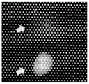
Fig. 6A is a diagram showing a fluorescence image of a microfluidic device using one embodiment of the present invention.
Fig. 6B is a diagram showing a fluorescence image using the microfluidic device of comparative example 1.
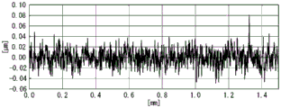
Fig. 7 is a graph showing measurement data of the surface roughness of the cover member of the microfluidic device according to the embodiment of the present invention.
Fig. 8 is a graph showing measurement data of the surface roughness of the cover member of the microfluidic device according to the embodiment of the present invention.
Fig. 9 is a graph showing measurement data of the surface roughness of the cover member of the microfluidic device of comparative example 2.
Fig. 10 is a graph showing measurement data of the surface roughness of the cover member of the microfluidic device of comparative example 3.
Detailed Description
One embodiment of the present invention is explained with reference to fig. 1 to 5. In the present specification, the dimensional ratios in the drawings are exaggerated for the purpose of illustration and do not necessarily correspond to actual dimensions.
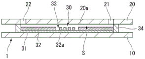
Fig. 1 is a perspective view showing a microfluidic device 1 of the present embodiment. Fig. 2 is a sectional view taken along line b-b of fig. 1. As shown in fig. 1 and 2, the microfluidic device 1 includes a microwell array 30 having a plurality of wells, and a cover member 20 facing the microwell array 30 in a spaced state, and has a flow path 35 between the microwell array 30 and the cover member 20. The microwell array 30 may have only the substrate 10, or may have a bottom layer 31 and a wall layer 32 in addition to the substrate 10. Peripheral member 34 is located between microwell array 30 and lid member 20. The region sandwiched between the microwell array 30 and the cover member 20 and surrounded by the peripheral member 34 is a flow path 35. The peripheral member 34 may also be integrally formed with the cover member 20.
The substrate 10 may also be transparent to electromagnetic waves. Here, the electromagnetic wave includes X-ray, ultraviolet ray, visible ray, infrared ray, and the like. The substrate 10 is transparent to electromagnetic waves, and fluorescence, phosphorescence, or the like generated by a reaction between a sample and a reagent enclosed in the microfluidic device 1 can be observed from the substrate 10 side.
The substrate 10 may transmit only electromagnetic waves in a predetermined wavelength range. For example, when the presence of the sample in the micropores is determined by detecting fluorescence having a peak in a wavelength range of 350 to 700nm, which is a visible light region, a substrate that can transmit at least visible light in the above wavelength range may be used as the substrate 10.
Examples of the material for forming the substrate 10 include glass and resin. Examples of the material of the resin substrate include ABS resin, polycarbonate resin, COC (cyclic olefin copolymer), COP (cyclic olefin polymer), acrylic resin, polyvinyl chloride, polystyrene resin, polyethylene resin, polypropylene resin, polyvinyl acetate, PET (polyethylene terephthalate), PEN (polyethylene naphthalate), and the like. These resins may also contain various additives. Examples of the additive include an antioxidant, an additive for imparting hydrophobicity, an additive for imparting hydrophilicity, and the like. The resin substrate may contain only one of the above resins, or may contain a mixture of a plurality of resins.
Since fluorescence or phosphorescence is utilized in a sample analysis method described later, a material substantially free of autofluorescence is used as the substrate 10. Here, "substantially free of autofluorescence" means that the substrate has no autofluorescence at all at the wavelength used for detection of the experimental result, or has autofluorescence at a level of weak fluorescence that does not affect detection of the experimental result. For example, if the autofluorescence is about 1/2 or less, preferably 1/10 or less, compared with the fluorescence of the detection target, the autofluorescence can be said to be weak fluorescence to such an extent that the detection of the experimental result is not affected.
The thickness of the substrate 10 may be appropriately determined, and is preferably 5 millimeters (mm) or less, more preferably 2mm or less, and still more preferably 1.6mm or less, for example, in order to allow fluorescence or phosphorescence emitted in sample analysis to be easily transmitted therethrough. For ease of processing, it is preferably 0.1mm or more, and more preferably 0.2mm or more, for example. The upper limit and the lower limit of the thickness of the substrate 10 may be arbitrarily combined. For example, the thickness of the substrate 10 is preferably 0.1mm or more and 5mm or less, more preferably 0.2mm or more and 2mm or less, and further preferably 0.4mm or more and 1.6mm or less.
The cover member 20 (may be simply referred to as a cover 20) is a plate-shaped or sheet-shaped member. The cover member 20 faces the microwell array 30 in a separated state. In other words, the cover member 20 covers the plurality of micropores 33. The flow path 35 is a region surrounded by the lid member 20, the micro-pore array 30, and the peripheral member 34. The flow path 35 is connected to the openings of the plurality of micropores 33 and positioned above the plurality of micropores 33.
The cover member 20 has a first hole 21 and a second hole 22 penetrating in the thickness direction. The first hole 21 and the second hole 22 are present so as to sandwich 1 or a plurality of the droplet holding portions in a plan view of the cover member 20. The first well 21 and the second well 22 communicate with the internal space S including the micro well array 30 and the flow path 35 in the completed microfluidic device 1. The first hole 21 and the second hole 22 function as an inlet for supplying fluid to the internal space S and an outlet for discharging fluid.
The material forming the cover member 20 or the thickness of the cover member 20 may be the same as the substrate 10.
When the cover member 20 has electromagnetic wave permeability, the electromagnetic wave permeability can be set as appropriate. For example, when the electromagnetic wave irradiation step described later is not performed from the cover member 20 side, the cover member 20 may be opaque to electromagnetic waves.
The arithmetic average roughness (Ra) of the surface 20a of the cover member 20 on the side of the microwell array 30 is 70nm or less, preferably 60nm or less, more preferably 50nm or less, still more preferably 40nm or less, and particularly preferably 35nm or less. Further, the arithmetic average roughness (Ra) of the surface 20a of the lid member 20 on the side of the microwell array 30 may be 30nm or less, or may be 25nm or less, or may be 20nm or less, or may be 15nm or less. When the arithmetic mean roughness (Ra) of the surface 20a of the cover member 20 on the side of the microwell array 30 is 50nm or less, non-specific adsorption of the reagent to the surface 20a of the cover member 20 on the side of the microwell array 30 can be suppressed.
The lower limit of the arithmetic average roughness (Ra) of the surface 20a of the cover member 20 on the side of the microwell array 30 is not particularly limited, and is, for example, 5 nm.
The upper limit value and the lower limit value of the arithmetic average roughness (Ra) of the surface 20a on the microwell array 30 side of the cover member 20 may be arbitrarily combined. For example, the arithmetic average roughness (Ra) of the surface 20a of the lid member 20 on the side of the pore array 30 may be 5nm or more and 70nm or less, 5nm or more and 60nm or less, 6nm or more and 50nm or less, 7nm or more and 40nm or less, 7nm or more and 35nm or less, 8nm or more and 30nm or less, 8nm or more and 25nm or less, 9nm or more and 20nm or less, or 10nm or more and 15nm or less.
The arithmetic average roughness (Ra) can be measured, for example, by a measuring method prescribed in JIS B0601-. The measurement range may be the entire surface of the cover member or may be a representative region. The measurement range in the present embodiment is defined as: is a straight line having the center of the cover member 20 as the center of the measurement range, and has a length of 800 μm to 1.5 mm.
The method of making the arithmetic mean roughness (Ra) of the surface 20a of the cover member 20 on the side of the microwell array 30 to be 50nm or less is not particularly limited, and examples thereof include mirror polishing of the cover member 20. When the cover member 20 is manufactured by injection molding, a mold of the cover member 20 may be mirror-finished by diamond grinding or the like.
The cover member 20 may have a contact angle with water of 70 degrees or more on the surface 20a on the microwell array 30 side.
Further, since the contact angle of the surface 20a of the cover member 20 on the side of the microwell array 30 with water is 180 degrees or less, the contact angle of the surface of the cover member 20 on the side of the microwell array 30 with water is, for example, 70 degrees or more and 180 degrees or less.
The contact angle with water can be measured, for example, by the sessile drop method prescribed in JIS R3257-1999. The contact angle may be measured by a method based on ASTM D5725-1997 in place of the static drop method prescribed in JIS R3257-1999.
The surface roughness (ten-point average roughness) (Rz) of the surface 20a of the cover member 20 on the side of the microwell array 30 is preferably 350nm or less, more preferably 300nm or less, and particularly preferably 250nm or less. Further, the surface roughness (ten-point average roughness) (Rz) of the surface 20a of the cover member 20 on the side of the microwell array 30 may be 200nm or less, may also be 150nm or less, may also be 120nm or less, may also be 110nm or less, may also be 100nm or less, and may also be 90nm or less. When the surface roughness (Rz) of the surface 20a on the microwell array 30 side of the cover member 20 is 350nm or less, non-specific adsorption of a reagent to the surface 20a on the microwell array 30 side of the cover member 20 can be further suppressed.
The lower limit of the surface roughness (ten-point average roughness) (Rz) of the surface 20a of the cover member 20 on the side of the microwell array 30 is not particularly limited, and is, for example, 50 nm.
The upper limit value and the lower limit value of the surface roughness (ten-point average roughness) (Rz) of the surface 20a on the microwell array 30 side of the cover member 20 may be arbitrarily combined. For example, the surface roughness (ten-point average roughness) (Rz) of the surface 20a of the cover member 20 on the side of the microwell array 30 may be 50nm or more and 350nm or less, 55nm or more and 300nm or less, 60nm or more and 250nm or less, 60nm or more and 200nm or less, 60nm or more and 150nm or less, 65nm or more and 120nm or less, 70nm or more and 110nm or less, 70nm or more and 100nm or less, or 80nm or more and 90nm or less.
The surface roughness (Rz) can be measured according to the measuring method specified in JIS B0601-2001. The measurement range may be the entire surface of the cover member or may be a representative region. The measurement range in the present embodiment is defined as: is a straight line having the center of the cover member 20 as the center of the measurement range and has a length of 800 μm to 1.5 mm.
The method of making the surface roughness (Rz) of the surface 20a of the cover member 20 on the microwell array 30 side 350nm or less is not particularly limited, and examples thereof include mirror polishing of the cover member 20. When the cover member 20 is manufactured by injection molding, a mold of the cover member 20 may be mirror-finished by diamond grinding or the like.
The surface 20a of the cover member 20 on the side of the microwell array 30 preferably has an Ra/Rz of 0.10 or more. The cover member 20 preferably has a surface 20a on the side of the microwell array 30 and an Ra/Rz of 0.24 or less, more preferably 0.23 or less, and still more preferably 0.225 or less. Further, Ra/Rz of the surface 20a of the cover member 20 on the side of the microwell array 30 may be 0.16 or less, may be 0.15 or less, may be 0.14 or less, and may be 0.13 or less.
The upper limit value and the lower limit value of Ra/Rz of the surface 20a on the microwell array 30 side of the cover member 20 may be arbitrarily combined. For example, the Ra/Rz of the surface 20a on the microwell array 30 side of the lid member 20 may be 0.10 or more and 0.24 or less, 0.10 or more and 0.23 or less, 0.10 or more and 0.225 or less, 0.10 or more and 0.16 or less, 0.10 or more and 0.15 or less, 0.10 or more and 0.14 or less, or 0.10 or more and 0.13 or less.
When Ra/Rz of the surface 20a of the cover member 20 on the side of the microwell array 30 is 0.10 or more and 0.24 or less, non-specific adsorption of a reagent to the surface 20a of the cover member 20 on the side of the microwell array 30 can be further suppressed even if the material of the cover member 20 is hydrophilic. This is considered to be because not only the relationship between the surface 20a of the cover member 20 on the side of the well array 30 and the reagent, which is an electric and chemical interaction, can be suppressed, but also the physical interaction can be suppressed because the minute irregularities of the surface 20a of the cover member 20 on the side of the well array 30 are small. When Ra/Rz is less than 0.10, it means that there is a partially protruding portion on the surface 20a of the cover member 20 on the microwell array 30 side, and it is presumed that nonspecific adsorption of a reagent is likely to occur at this portion. When Ra/Rz is more than 0.24, it means that the entire surface 20a of the cover member 20 on the side of the microwell array 30 is rough, and it is estimated that nonspecific adsorption of reagents is likely to occur.
The microfluidic device of the present embodiment may be replaced with an arithmetic average roughness (Ra) within the above range by applying hydrophobic coating to the surface 20a of the cover member 20 on the side of the micro-pore array 30. Therefore, by applying hydrophobic coating to the surface 20a on the microwell array 30 side of the cover member 20, nonspecific adsorption of reagents to the surface 20a on the microwell array 30 side of the cover member 20 can be suppressed.
Examples of a method for hydrophobic coating of the surface 20a of the cover member 20 on the side of the microwell array 30 include a method in which a hydrophobic coating agent is applied to the surface 20a of the cover member 20 on the side of the microwell array 30 and dried.
Examples of the coating agent include a fluorine-based coating agent, a fluoropolymer, and a silicone resin. Examples of the coating method include a dry coating method and a wet coating method.
The thickness of the coating layer when the hydrophobic coating agent is coated on the surface 20a of the cover member 20 on the side of the micropore array 30 is preferably 0.01 μm or more and 3 μm or less, more preferably 0.05 μm or more and 1 μm or less.
The microwell array 30 may also have a bottom layer 31, a wall layer 32 (also referred to as a partition 32), and a plurality of microwells 33. The bottom layer 31 is disposed on the substrate 10. The wall layer 32 is formed on the bottom layer 31. The plurality of micropores 33 are formed by the bottom layer 31 and a plurality of through holes 32a formed in the thickness direction of the wall layer 32. The plurality of micropores 33 are formed in an array in the wall layer 32. In the internal space S between the substrate 10 and the lid member 20, there is a gap between the microwell array 30 and the lid member 20, in other words, between the upper surface of the wall layer 32 and the lid member 20. The voids function as flow paths communicating with the micropores 33 and the first and second holes 21 and 22.
In the case where the properties of the bottom surfaces of the pores 33 are the same as those of the substrate 10 and there is no problem, the wall layer 32 may be formed directly on the substrate 10 without providing the bottom layer 31. Therefore, at this time, the surface of the substrate 10 and the through-holes 32a of the wall layer 32 constitute the micropores 33.
The wall layer 32 has a plurality of through holes 32a arranged in an array as viewed in the thickness direction. The inner surface of each through hole 32a constitutes the inner wall surface of each micro hole 33.
Further, the wall layer 32 may be formed integrally with the substrate 10. Therefore, at this time, the micropores 33 are formed on the surface of the substrate 10.
As a material for forming the wall layer 32, the same resin as that for forming the substrate 10 can be used, but a material in which a colored component that absorbs electromagnetic waves of a predetermined wavelength is mixed with a resin can also be used.
As the resin material, either a hydrophilic resin whose molecules constituting the resin have hydrophilic groups or a hydrophobic resin whose molecules constituting the resin have hydrophobic groups can be used in consideration of the properties required for the micropores 33.
Examples of the hydrophilic group include a hydroxyl group, a carboxyl group, a sulfo group, a sulfonyl group, an amino group, an amide group, an ether group, and an ester group. As the hydrophilic resin, for example, silicone polymers; an epoxy resin; a polyethylene resin; a polyester resin; a polyurethane resin; a polyacrylamide resin; a polyvinylpyrrolidone resin; acrylic resins such as polyacrylic acid copolymers; polyvinyl alcohol resins such as cationized polyvinyl alcohol, silanized polyvinyl alcohol, and sulfonated polyvinyl alcohol; a polyvinyl acetal resin; a polyvinyl butyral resin; a polyethylene polyamide resin; a polyamide polyamine resin; cellulose derivatives such as hydroxymethylcellulose and methylcellulose; polyoxyalkylene derivatives such as polyethylene oxide and polyethylene oxide-propylene oxide copolymers; a maleic anhydride copolymer; ethylene-vinyl acetate copolymers; styrene-butadiene copolymers; and combinations of the above resins, and the like.
Examples of the hydrophobic resin include, for example, a novolak resin; acrylic resin; a methacrylic resin; a styrene resin; vinyl chloride resin; vinylidene chloride resin; a polyolefin resin; a polyamide resin; a polyimide resin; a polyacetal resin; a polycarbonate resin; polyphenylene sulfide resin; polysulfone resin; a fluororesin; a silicone resin; urea-formaldehyde resin; a melamine resin; a guanamine resin; a phenolic resin; a cellulose resin; and combinations of the above resins, and the like, and those having a contact angle of 70 degrees or more as measured by the sessile drop method prescribed in JIS R3257-1999 are suitably selected and used. That is, the term "hydrophobicity" as used herein means a contact angle of 70 degrees or more as measured by the sessile drop method defined in JIS R3257-1999. Further, the contact angle may be measured by a method based on ASTM D5725-1997 in place of the sessile drop method prescribed in JIS R3257-1999.
Either one of the hydrophilic resin and the hydrophobic resin may be a thermoplastic resin or a thermosetting resin. Further, the resin may be a resin cured by an active energy ray such as an electron beam or UV light, or may be an elastomer.
When a photoresist is used as the resin material, a large number of fine through holes 32a can be formed in the wall layer 32 with high accuracy by photolithography.
When the photolithography method is used, a known means can be appropriately selected for selection of the kind of the photoresist to be used, coating and exposure (sensitization), and a method for removing unnecessary photoresist.
When a resist is not used, the wall layer 32 can be formed by injection molding or the like, for example.
As the colored component, an organic or inorganic pigment may be exemplified. Specific examples of the black pigment include carbon black, acetylene black, and iron black. Examples of the yellow pigment include chrome yellow, zinc yellow, yellow soil, sunfast yellow, permanent yellow and gasoline yellow. Examples of orange pigments include orange lake, molybdate orange, and gasoline orange. Examples of red pigments include iron oxide red, cadmium red, vermilion, permanent red, lithol red, lake red, brilliant scarlet and thioindigo red. Examples of the blue pigment include ultramarine blue, cobalt blue, phthalocyanine blue, tencel blue and indigo blue. Examples of the green pigment include chromium green, naphthol chromium green, and phthalocyanine green.
In addition, when the wall layer 32 is formed by injection molding or the like, not only a pigment dispersed in a resin, but also various dyes dissolved in a resin may be used as a colored component. Dyes can be exemplified according to various dye processes. Specific examples thereof include direct dyes, basic dyes, cationic dyes, acid dyes, mordant dyes, sulfur dyes, vat dyes, naphthol dyes, disperse dyes, and reactive dyes. In particular, when a resin is dyed, a disperse dye is selected.
In the present specification, the micropore means a cell having a volume of 10 nanoliters (nL) or less. By making the volume of the microwell 33 small to such an extent, it is possible to preferably perform an enzyme reaction which proceeds in a minute space, such as PCR and ICA (invaded cleavage Assay) reaction. For example, mutation detection of a gene can be performed by digital PCR.
The volume of the micropores 33 is not particularly limited, but is preferably 10 femtoliters (fL) or more and 100 picoliters (pL) or less, more preferably 10fL or more and 5pL or less, and most preferably 10fL or more and 2pL or less. When the volume is set within this range, it is preferable that only 1 to several biomolecules or carriers are accommodated in 1 microwell 33 in the sample analysis described later.
The shape of the micropores 33 is not particularly limited as long as the volume is within the above range. Therefore, for example, the shape of a cylinder, a polyhedron having a plurality of faces (for example, a rectangular parallelepiped, a hexagonal prism, an octagonal prism, or the like), an inverted cone, an inverted pyramid, an inverted polygonal cone (for example, an inverted triangular cone, an inverted quadrangular cone, an inverted pentagonal cone, an inverted hexagonal cone, and an inverted polygonal cone having seven or more angles), or the like can be used.
Further, the shape of the plurality of micropores 33 may be a combination of 2 or more of the above shapes. For example, a part of the plurality of micropores 33 may be cylindrical and the rest may be inverted conical. When the micropores 33 have an inverted conical shape or a chamfered conical shape, the bottom surface of the conical shape or the pyramidal shape serves as an opening portion for communicating the flow path 35 and the micropores 33. In this case, the bottom of the micropore 33 may be flattened by cutting a part of the top of the inverse cone or the chamfered cone. In other examples, the bottom of micropore 33 may have a curved shape protruding toward the opening, or the bottom of micropore 33 may have a curved shape recessed.
The thickness of the wall layer 32 determines the depth of the micropores 33. When the micropores are cylindrical, the thickness of the wall layer 32 may be, for example, 10nm to 100 μm, preferably 100nm to 50 μm, more preferably 1 μm to 30 μm, further preferably 2 μm to 15 μm, and further preferably 3 μm to 10 μm, in order to enclose an aqueous liquid (sample) containing biomolecules.
The size of each part of the microwells 33 may be appropriately determined so that 1 or more biomolecules are accommodated in 1 microwell, considering the amount of aqueous liquid to be accommodated, the size of a carrier such as beads to which biomolecules are attached, and the like.
The number or density of micropores 33 provided in micropore array 30 can be set as appropriate.
Every 1cm2The number of micropores 33 is, for example, 1 to 1000 ten thousand, preferably 10 to 500 ten thousand, and more preferably 10 to 100 ten thousand. In the present specification, the thickness of the resin composition is sometimes 1cm2The number of micropores 33 is referred to as the density of micropores. When the density of the micropores is within this range, the operation of sealing the aqueous liquid as a sample in a predetermined number of cells is easy. In addition, when the density of the micropores is within this range, observation of the wells for analyzing the experimental results is also easy. For example, when mutation in a cell-free DNA is detected, it is preferable to use, for example, about 100 to 200 ten thousand microwells when the percentage of mutant DNA to be detected is about 0.01% relative to the wild-type DNA.
Fig. 1 shows an example of a one-dimensional array in which a plurality of micropores 33 are aligned in a line. However, when a plurality of micropores are provided as described above, a two-dimensional array in which a plurality of micropores are two-dimensionally arranged may be used.
A peripheral member 34 having a frame shape in plan view is disposed around the micropore array. The peripheral member 34 in the thickness direction of the microfluidic device 1 has a larger dimension than the wall layer 32. The peripheral member 34 supports the lid member 20, and maintains the flow path 35 by securing a gap between the lid member 20 and the micro-pore array. That is, the flow path 35 is a region sandwiched between the microwell array 30 and the cover member 20 and surrounded by the peripheral member 34.
The material and the like of the peripheral member 34 are not particularly limited, and examples thereof include a double-sided tape in which an acrylic pressure-sensitive adhesive is laminated on both sides of a core film made of silicone rubber or acrylic foam.
Further, the peripheral member 34 may also be integrally formed with the cover member 20. At this time, the peripheral member 34 serves as a stepped portion of the lid member 20, and a gap is secured between the lid member 20 and the microwell array by the stepped portion to maintain the flow path 35.
The microfluidic device 1 configured as above may be manufactured, for example, in the following order.
First, the substrate 10 is prepared, and a wall resin layer to be the wall layer 32 is formed on the surface of the substrate 10. When the bottom layer 31 is provided, the bottom layer 31 is formed before the wall resin layer is formed. Even when the bottom layer 31 is not provided, an anchor layer or the like for improving adhesion between the substrate 10 and the wall resin layer may be provided on the surface of the substrate 10 as necessary.
The wall resin layer may be formed of a material in which a colored component is mixed in a resin material. When the resin material is a resist, the content of the colored component may be, for example, 0.5 mass% (mass%) or more and 60 mass% or less based on the total mass of the resin material and the colored component. The content is preferably 5% by mass or more and 55% by mass or less, and more preferably 20% by mass or more and 50% by mass or less. The content ratio of the color component to the total mass of the resin material and the color component may be appropriately set in consideration of the ratio of the photosensitive component or the like contained in the resist so that a desired pattern can be formed. When the coloring component is a pigment, the particle size of the pigment is set and prepared so as to satisfy the above-described predetermined condition with respect to the micropores to be formed. A dispersant may be added to the resin material together with the pigment as appropriate.
When the wall resin layer formed is formed of a material in which a color component is mixed in a resin material, the wall resin layer has a color based on the color component contained in the wall resin layer.
Next, through-holes 32a are formed in the formed wall resin layer. As described above, when the photolithography method is used, the through-hole 32a can be formed easily and accurately. When the wall resin layer is formed by injection molding or the like, the wall resin layer and the through hole can be formed in the same process. In addition, the through-holes 32a may be formed by etching using a pattern mask or the like.
When the through-hole 32a is formed, the wall resin layer becomes the wall layer 32, and the microwell array 30 is completed.
After that, the peripheral member 34 is disposed around the micropore array 30, and then the lid member 20 is disposed on the peripheral member 34. At this time, the cover member 20 is disposed so that the Ra of the surface 20a on the side of the microwell array 30 becomes 50nm or less. Next, when the substrate 10, the peripheral member 34, and the cover member 20 are integrally joined, the microfluidic device 1 is completed. A flow path is formed between the cover member 20 and the substrate 10 through the peripheral member 34. The bonding method is not particularly limited, and examples thereof include bonding with an adhesive, bonding with a double-sided tape, and bonding by laser welding.
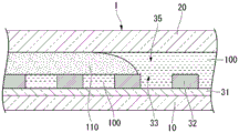
In addition, the microfluidic device 1 may integrally form the substrate 10 and the wall layer 32, or may integrally form the peripheral member 34 and the lid member 20. Fig. 3 shows the microfluidic device 2 in which the substrate 10 and the wall layer 32 are integrally formed, and the peripheral member 34 and the lid member 20 are integrally formed. The microfluidic device 2 can be manufactured as follows: the substrate 10 formed integrally with the wall layer 32 is disposed on the lid member 20 formed integrally with the peripheral member 34, and the stepped portion formed by integrally forming the peripheral member 34 and the lid member 20 is joined to the substrate 10 formed integrally with the wall layer 32. The flow path 35 is formed between the cover member 20 and the substrate 10 by a step portion formed on the cover member 20.
The configuration of the microfluidic device 2 is the same as that of the microfluidic device 1 described above except that the substrate 10 and the wall layer 32 are integrally formed, and the peripheral member 34 and the lid member 20 are integrally formed.
Alternatively, the substrate 10 and the wall layer 32 may be provided as separate elements, and the peripheral member 34 and the lid member 20 may be integrally formed as a microfluidic device. Also at this time, the configuration of the microfluidic device other than integrally forming the peripheral member 34 and the lid member 20 is the same as that of the microfluidic device 1 described above.
Next, a sample analysis method according to the present embodiment using the microfluidic device 1 according to the present embodiment will be described with reference to fig. 4 and 5.
The sample analysis method of the present embodiment is a sample analysis method using the microfluidic device 1 of the present embodiment, and includes:
introducing an aqueous liquid containing a sample into the flow path 35;
introducing a blocking liquid into the channel 35 to replace the aqueous liquid present in the channel 35, thereby enclosing the aqueous liquid in the micropores 33;
heating the microfluidic device to cause a reaction in the microwells 33, generating a signal for detection; and
the signal is detected.
Here, the aqueous liquid may contain water, a buffer, a detection reaction reagent, and the like in addition to the sample. The aqueous liquid may further contain an enzyme. For example, when the sample is a nucleic acid, PCR method, ICA method, LAMP method (Loop-Mediated Isothermal Amplification, registered trademark), TaqMan method (registered trademark), fluorescence probe method, or the like can be used. For example, when the sample is a protein, ELISA method (registered trademark) or the like can be used. Further, an additive such as a surfactant may be contained in the aqueous liquid.
Examples of the buffer include Tris-HCl buffer, acetate buffer, and phosphate buffer.
Examples of the enzyme include DNA polymerase, RNA polymerase, reverse transcriptase, and flanking endonuclease.
Examples of the surfactant include Tween 20 (also referred to as polyoxyethylene sorbitan monolaurate), Triton-X100 (also referred to as polyethylene glycol mono-4-octylphenyl ether (n about 10)), glycerin, octylphenol ethoxylate, and alkyl glycoside.
The microfluidic device of the present embodiment may preferably retain the aqueous liquid in the wells even when the temperature of the enclosed aqueous liquid is changed, for example, in gene mutation detection or the like. The range of the temperature to be changed, i.e., the range of the lower limit value to the upper limit value of the temperature change is, for example, 0 to 100 ℃, preferably 0 to 80 ℃, and more preferably 20 to 70 ℃. When the aqueous solution enclosed in the well is within this range, a reaction which proceeds in a minute space such as PCR or ICA reaction can be preferably performed.
Examples of the sample to be analyzed using the microfluidic device 1 of the present embodiment include DNA, RNA, miRNA, mRNA, protein, lipid, cell, and bacterium. The sample may be a sample collected from a living body such as blood. The detection target to be detected by sample analysis may be a PCR product obtained using DNA contained in the sample as a template, or may be an artificially synthesized compound (for example, an artificially synthesized nucleic acid obtained by simulating DNA as a sample). For example, when DNA that is a biomolecule is a detection target, the well may have a shape and a size into which 1 molecule of DNA enters.
The details of the sample analysis method will be described below. As a preparatory step, an aqueous liquid containing a sample enclosed in the microwells is prepared. The aqueous liquid containing the sample is a liquid containing water to be detected as a main solvent, and examples thereof include a PCR reaction solution containing a biological sample as a template and SYBR Green as a detection reagent, and an ICA reaction solution containing an allele probe, an ICA oligonucleotide, FEN-1, a fluorogenic substrate and the like. Surfactants can also be added during preparation to make the sample more easily enter the micropores. In addition, beads that specifically recognize the detection target may be added to capture the detection target in advance. The detection target may be suspended in an aqueous liquid without being directly or indirectly bound to a carrier such as a bead.
Next, the prepared aqueous liquid 100 containing the sample is introduced into the flow channel 35 from the first hole 21 using a syringe or the like (also referred to as a sample supply step). The supplied aqueous liquid 100 containing the sample is filled in each of the micropores 33 and the flow path 35 as shown in FIG. 4. The gas in the flow path 35 is removed by a degassing operation before the sample supply step. This degassing operation can be performed by filling the flow path 35 with a buffer solution. Examples of the buffer include water, water containing a buffer, water containing a surfactant, and water containing a buffer and a surfactant.
Next, an enclosing step of enclosing the aqueous liquid containing the sample 100 in the micropores 33 is performed. Before the sealing step, a label such as fluorescence may be added to the detection target in the sample contained in the aqueous liquid. The fluorescent labeling treatment may be performed before the sample supply step, for example, at the time of sample preparation, or the fluorescent label may be introduced into the channel 35 after the sample supply step.
In the sealing step, the sealing liquid 110 is supplied from the first hole 21 to the channel 35 using a syringe or the like. The supplied blocking liquid 110 flows through the channel, and as shown in fig. 5, the aqueous liquid 100 containing the sample present in the channel 35 is pushed toward the second hole 22. Further, the blocking liquid 110 is replaced with the aqueous medium 100 filled in the flow path 35, and the flow path 35 is filled with the blocking liquid 110. As a result, the aqueous liquid 100 containing the sample is disposed in the micropores 33 independently of each other, and the enclosing of the sample is completed.
In the present specification, the blocking liquid 110 is a liquid used to isolate the aqueous liquids introduced into the respective wells 33 of the well array 30 from each other without mixing, and examples thereof include oils. Examples of the oil include mineral oil used for PCR reaction, and the trade name "FC 40" manufactured by Sigma or "HFE-7500" manufactured by 3M.
The sealing liquid 110 preferably has a contact angle of 5 degrees or more and 30 degrees or less with respect to the material of the wall layer 32. When the contact angle of the sealing liquid 110 is in this range, the sealing liquid 110 is likely to press the aqueous liquid 100, and the aqueous liquid 10 is less likely to remain on the surface of the lid member 20. As a result, the sample can be preferably enclosed in each of the micropores 33. The contact angle of the blocking liquid may be measured, for example, by the sessile drop method defined in JIS R3257-1999 using the blocking liquid in place of water. Further, the contact angle may be measured by a method based on ASTM D5725-1997 in place of the sessile drop method prescribed in JIS R3257-1999.
Then, the following reaction steps were carried out: heating the microfluidic device 1 causes a reaction in the microwells 33, generating a signal for detection.
Examples of the signal used for detection include fluorescence, chemiluminescence, color development, potential change, pH change, and the like, but fluorescence is preferable.
Before the reaction step, the microfluidic device 1 may be placed in a thermal cycler to perform an enzymatic reaction such as a PCR reaction or an ICA reaction, if necessary.
The reaction may be, for example, a biochemical reaction, more specifically an enzymatic reaction. The temperature during heating is appropriately determined depending on the reaction, and is, for example, 60 ℃ to 100 ℃. The temperature at the time of heating is not the actual temperature of the reagent solution in the wells 33, but the heating temperature of the micro-fluid device set by a thermal cycler, incubator, or the like. The temperature at the time of heating is, for example, 60 ℃ or higher and 100 ℃ or lower, means that the maximum temperature is 60 ℃ or higher and 100 ℃ or lower, and is not necessarily maintained at 60 ℃ or higher and 100 ℃ or lower. That is, it is irrelevant that the temperature of the micro-fluid device 1 changes within the above-described temperature range. An example of the reaction is a signal amplification reaction. The signal amplification reaction is an isothermal reaction in which the microfluidic device 1 is maintained at a predetermined temperature, for example, 60 ℃ or higher and 100 ℃ or lower for a predetermined time, for example, at least 10 minutes, preferably about 15 minutes, under a condition that a reagent solution containing an enzyme for signal amplification is contained in the wells 33.
Next, a signal generated from the microwell 33 by the above reaction is detected (detection step). For example, when the signal is fluorescence, the fluorescence microscope is installed and excitation light (electromagnetic wave) is irradiated. The wavelength of the excitation light is appropriately set according to the fluorescent label used.
The irradiation of the electromagnetic wave may be performed from the substrate 10 side of the micro-fluid device 1, may be performed from the cover member 20 side, that is, the upper side of the micro-pores 33, or may be performed from any other direction. In addition, the detection of fluorescence or phosphorescence generated as a result of electromagnetic wave irradiation may be performed from the substrate side of the microwell array, from the well side, or from any other direction, and for example, when fluorescence or phosphorescence is detected using a fluorescence microscope, it is simple to perform it from the substrate 10 side of the microfluidic device 1.
Next, fluorescence or phosphorescence emitted from several microwells 33 among the plurality of microwells 33 constituting the microwell array 30 is measured. The measurement may be performed by taking a fluorescence image of microwell array 30, using the fluorescence image.
For example, by performing a PCR reaction in the microwell array 30 and detecting fluorescence of SYBR Green in the microwells 33 in which PCR amplification is observed, the ratio of the number of microwells 33 in which amplification is observed to the number of all microwells 33 can be calculated. When the object to be detected is, for example, a Single Nucleotide Polymorphism (SNP), the frequency of occurrence of the SNP can be analyzed by counting the number of microwells 33 that emit fluorescence.
In this measurement step, the aqueous liquid may contain a protein or an enzyme as a sample or an enzyme as a reagent. When these proteins or enzymes are suspended in an aqueous liquid without being adsorbed by the beads, adsorption of the proteins or enzymes to the surface of the cover member 20 is particularly likely to occur. Proteins or enzymes are non-specifically adsorbed on the cover member 20, and when these proteins or enzymes emit fluorescence or phosphorescence, the fluorescence or phosphorescence is detected as noise. According to the microchannel device of the present invention, since adsorption of proteins or enzymes contained in a sample or a reagent to the lid member 20 is reduced, generation of noise can be suppressed.
Another aspect of the present invention includes the following.
[8] A microfluidic device comprising a microwell array having a plurality of microwells and a cover member facing the microwell array in a separated state, wherein a flow path is provided between the microwell array and the cover member, the arithmetic average roughness Ra of the surface of the cover member on the microwell array side is 5nm to 50nm, and the ten-point average roughness (Rz) is 50nm to 250 nm.
[9] The microfluidic device of [8], further having a peripheral member located between the array of microwells and the cover member and surrounding the flow path.
[10] The microfluidic device according to [9], wherein the peripheral member is a stepped portion integrally formed with the lid member.
[11] The microfluidic device according to any one of [8] to [10], wherein a contact angle of a surface of the cover member on the micropore array side with water is 70 degrees or more.
[12] The microfluidic device according to any one of [8] to [11], wherein Ra/Rz of the surface on the microwell array side of the cover member is 0.10 or more and 0.23 or less.
[13] The microfluidic device according to any one of [8] to [12], wherein a surface on the microwell array side of the cover member is subjected to hydrophobic coating.
[14] The microfluidic device according to any one of [8] to [13], wherein the hydrophobic coating is 1 of a fluorine-based coating agent, a fluoropolymer, and a silicone resin.
[15] A sample analysis method using the microfluidic device according to any one of [8] to [14], the sample analysis method comprising:
supplying an aqueous liquid containing a sample to the flow path;
introducing a blocking liquid into the channel to replace the blocking liquid with the aqueous liquid present in the channel, thereby enclosing the aqueous liquid in the micropores;
Causing a reaction in the microwell, producing a signal for detection; and
the signal is detected.
[16] The method for analyzing a sample according to [15], wherein the sample is DNA, RNA, protein, lipid, cell or bacterium.
Examples
The present invention will be described in more detail with reference to the following examples, but the present invention is not limited to the following examples.
(example 1)
2 resin members were prepared, which were formed by injection molding of a rectangular substrate made of COP (ZEONOR1010R, manufactured by Zeon corporation, japan) and a rectangular cover member made of COP. For the COP substrate, cylindrical minute holes having a diameter of 10 μm and a depth of 15 μm were disposed over the entire surface of the substrate, and the substrate was injection molded. The cover member is formed with a step portion having a height of 100 μm, i.e., a peripheral member, an inlet and an outlet. The inlet and the outlet are disposed inside the peripheral member along the longitudinal direction of the cover member.
The surface of the mold of the steel cover member corresponding to the bottom surface of the cover member (the surface on which the stepped portion was formed) was polished by #3000 diamond grinding to perform mirror finishing of the mold.
The contact angle of the bottom surface of the formed lid member with water was measured by the static drop method prescribed in JIS R3257-. The contact angle with water of the bottom surface of the lid member of example 1 was 85 degrees.
The surface roughness of the formed lid member was measured by a contact surface roughness measuring instrument (talyurf PGI1240, manufactured by Taylor Hobson). In this measurement, a height difference from the starting point (height 0nm) in the scanning range of 800 μm was obtained.
Table 1 shows the measurement results of Ra and Rz of the bottom surface of the cover member.
TABLE 1

The substrate made of COP and the lid member were bonded to each other by applying mineral oil to the stepped portion of the lid member so that the mirror-finished surface of the lid member became the substrate side, thereby producing a microfluidic device.
200. mu.L of a buffer solution having a composition shown in Table 2 below was fed into the channel between the substrate and the cover member, and the buffer solution was filled into each well of the micro-well chip.
TABLE 2
| Buffer composition | Final concentration |
| MgCl2 | 20mM |
| Tris(pH8.5) | 50mM |
| Tween20 | 0.05% |
Then, 10. mu.L of a fluorescent reagent (Fluoroescein, Tokyo chemical industries, Ltd.) having a composition shown in Table 3 below was fed into the channel, and the buffer solution was replaced with the fluorescent reagent. Then, 150. mu.l of fluorocarbon oil (FC40, Sigma) was fed to the micro-well chip, and the wells of the micro-well chip were sealed. In this example, although the fluorescence reaction is not performed, an enzyme is added to the fluorescent reagent so that the fluorescence reaction is performed in the same state.
TABLE 3
| Fluorescent reagent composition | Final concentration |
| Fluorescent reagent | 2μM |
| MgCl2 | 20mM |
| Tris(pH8.5) | 50mM |
| Flanking endonuclease 1 | 0.1mg/ml |
| Tween20 | 0.05% |
The above-mentioned microfluid device was mounted on a hot plate, heated at 66 ℃ for 15 minutes, and then a fluorescence image of the micro-well chip was observed with a fluorescence microscope (BZ-710, manufactured by KEYENCE) using a 4-fold objective lens. The exposure time was set to 20msec in a bright field, and the fluorescence filter using GFP (Green Fluorescent Protein) was set to 3000 msec.
Fig. 6A shows the fluorescence observation result of the micro-well chip after droplet formation in the microfluidic device of example 1. The size of the observed image was 580. mu. m.times.580. mu.m. In the microfluidic device of example 1, the reagent was not non-specifically adsorbed on the bottom surface of the cover member, and the number of droplets was accurately measured.
Comparative example 1
A microfluidic device was produced in the same manner as in example 1, except that the surface of the mold corresponding to the bottom surface of the lid member was not mirror-finished. The measurement results of Ra and Rz of the bottom surface of the lid member are shown in table 1. The contact angle of the bottom surface of the lid member of comparative example 1 with water was 85 degrees.
In the microfluidic device fabricated as described above, the buffer solution and the fluorescent reagent were fed in the same manner as in example 1 to form droplets, and the fluorescence image of the micro-well chip was observed.
Fig. 6B shows the result of fluorescence observation of the micro-well chip after droplet formation in the microfluidic device of comparative example 1. The arrowed portions in the figure indicate representative reagent attachments. In addition to the arrow part, a large amount of the reagent attachment was also seen in the entire visual field.
As shown in fig. 6B, in the microfluidic device of comparative example 1 using a non-mirror-finished cover member, the reagent was non-specifically adsorbed on the bottom surface of the cover member, and the position of attachment resulted in failure to measure the accurate number of droplets.
From these results, it was found that even when the contact angle between the bottom surface of the cover member and water was the same, nonspecific adsorption of the reagent to the bottom surface of the cover member was reduced by Ra of 50nm or less.
(example 2)
A COP substrate was produced in the same manner as in example 1. A cap member made of COP was produced in the same manner as in example 1, except that the time for mirror-finishing the surface corresponding to the bottom surface of the cap member in the mold of the cap member was extended. The surface roughness of the formed lid member was measured using a surface roughness measuring instrument (SJ-210, manufactured by Mitutoyo). The scanning range of this measurement was 1.5mm in the direction perpendicular to the longitudinal direction of the cover member with the center of the cover member as the center of the scanning range, and a step difference from the starting point (height of 0nm) was obtained. Table 4 shows the measurement results of Ra and Rz of the bottom surface of the lid member of example 2. Fig. 7 is a graph showing measurement data of the surface roughness of the cover member of the microfluidic device of example 2.
TABLE 4
| Ra(nm) | Rz(nm) | Ra/Rz | Adsorption area (%) | Evaluation of | |
| Example 2 | 11 | 87 | 0.126 | 1.8 | Good taste |
| Example 3 | 32 | 237 | 0.135 | 3.6 | Good taste |
| Comparative example 2 | 71 | 378 | 0.187 | 22.3 | Difference (D) |
| Comparative example 3 | 138 | 837 | 0.164 | 21.0 | Difference (D) |
The base material and the lid member were bonded to each other by applying mineral oil to the stepped portion of the lid member so that the mirror-finished surface of the lid member became the substrate side, thereby producing a microfluidic device.
The buffer solution, the fluorescent reagent and the mineral oil were delivered to the microfluidic device under the same conditions as in example 1, and the fluorescent reagent was individually sealed in each well of the micro-well chip. In this example, the fluorescence reaction was not performed as in example 1, but an enzyme was added to the fluorescent reagent in order to bring the state into the same state as when the fluorescence reaction was performed.
The above-mentioned microfluid device was mounted on a hot plate, heated at 66 ℃ for 15 minutes, and then a fluorescence image of the micro-well chip was observed with a fluorescence microscope (BZ-710, manufactured by KEYENCE) using a 4-fold objective lens. The exposure time was set to 20msec in a bright field, and the fluorescence filter using GFP (Green Fluorescent Protein) was set to 3000 msec. The field of view was 3.6mm by 2.7 mm.
In the fluorescence image, when the target molecule is present in the well, a region emitting fluorescence intensity equal to or higher than a reference is determined as a portion to which the fluorescent reagent is adsorbed, based on the intensity of fluorescence emitted by the enzyme reaction, and the area of the portion to which the fluorescent reagent is adsorbed is calculated.
The ratio (%) of the area of the portion where the fluorescent reagent was adsorbed to the area of the entire fluorescence image was determined as the adsorption area. When the ratio of the adsorption area is less than 10%, the inhibition of adsorption is good, and when the ratio is 10% or more, the inhibition of adsorption is poor. The results are shown in table 4.
(example 3)
The ratio of the reagent adsorption area in example 3 was determined in the same manner as in example 2, except that the time for mirror-finishing the surface corresponding to the bottom surface of the lid member in the mold for the lid member was shortened. The results are shown in table 4. Fig. 8 is a graph showing measurement data of the surface roughness of the cover member of the microfluidic device of example 3.
Comparative examples 2 and 3
The ratios of the reagent adsorption areas of comparative examples 2 and 3 were determined in the same manner as in example 2, except that the surface of the mold of the lid member corresponding to the bottom surface of the lid member was not mirror-finished. The results are shown in table 4. Fig. 9 and 10 show measurement data of the surface roughness of the lid member of the microfluidic devices of comparative examples 2 and 3, respectively.
In examples 2 and 3 in which Ra of the bottom surface of the lid member, i.e., the surface of the lid member on the side of the microwell array was 70nm or less, the ratio of the adsorption area was 1.8% and 3.6%, respectively, which were good values.
On the other hand, in comparative examples 2 and 3 in which the Ra of the surface on the microwell array side of the lid member was larger than 70nm, the ratio of the adsorption area was 22.3% and 21.0%, respectively. In comparative examples 2 and 3, since the surface of the mold of the lid member corresponding to the bottom surface of the lid member was not mirror-finished, the surface roughness of the bottom surface of the lid member could not be controlled, and unevenness occurred in the surface roughness.
The reason why the suppression of adsorption is evaluated to be good when the ratio of the adsorption area is less than 10% is as follows.
When the ratio of the adsorption area exceeds 10%, for example, when a low concentration sample of only 1 target molecule is to be measured in all the wells of the microfluidic device, the target molecule is enclosed in the well overlapping with the portion where the reagent is adsorbed with a probability of 10% or more. Even if the wells of the reagent-adsorbed portion emit light due to the enzyme reaction, the emission cannot be detected, and the result is erroneously determined as negative (false negative). Even if 2 identical measurements were performed, false negatives were obtained with a probability of 1% or more (1 or more out of 100).
On the other hand, when the ratio of the adsorption area is less than 10%, for example, when the ratio of the adsorption area is 5% or less as in examples 2 and 3, the probability of false negative becomes 5% or less, and the probability of false negative can be reduced to 0.25% or less by performing 2 times of the same measurement.
Industrial applicability
According to the present invention, it is possible to provide a microfluidic device and a sample analysis method capable of detecting fluorescence or phosphorescence of an aqueous liquid in a well as accurately as possible. For example, in the case of diagnosis or the like by detection of DNA, RNA or the like derived from a living body, nucleic acid may be put into a minute space together with a reagent.
Description of the symbols
1 microfluidic device
10 base plate
20 cover component
30 microwell array
32 wall layers
33 micro-pores
100 aqueous liquid
110 sealing liquid
Claims (7)
1. A microfluidic device comprising a microwell array having a plurality of microwells and a cover member facing the microwell array in a separated state, wherein a flow path is provided between the microwell array and the cover member, and the arithmetic average roughness Ra of the surface of the cover member on the microwell array side is 70nm or less.
2. The microfluidic device according to claim 1, wherein a contact angle with water of a surface on the microwell array side of the cover member is 70 degrees or more.
3. The microfluidic device according to claim 1 or 2, wherein a surface roughness Rz of a surface on the microwell array side of the cover member is 350nm or less.
4. The microfluidic device according to any one of claims 1 to 3, wherein Ra/Rz of the surface on the microwell array side of the cover member is 0.10 or more and 0.24 or less.
5. The microfluidic device according to any one of claims 1 to 4, wherein a surface on the microwell array side of the cover member is subjected to hydrophobic coating.
6. A sample analysis method using the microfluidic device according to any one of claims 1 to 5, comprising:
supplying an aqueous liquid containing a sample into the flow path;
introducing a blocking liquid into the channel to replace the blocking liquid with the aqueous liquid present in the channel, thereby enclosing the aqueous liquid in the micropores;
heating the microfluidic device to cause a reaction in the microwells to generate a signal for detection; and
the signal is detected.
7. The method for analyzing a sample according to claim 6, wherein the sample is DNA, RNA, protein, lipid, cell, or bacterium.
Applications Claiming Priority (3)
| Application Number | Priority Date | Filing Date | Title |
|---|---|---|---|
| JP2019037543 | 2019-03-01 | ||
| JP2019-037543 | 2019-03-01 | ||
| PCT/JP2020/006402 WO2020179442A1 (en) | 2019-03-01 | 2020-02-19 | Microfluidic device and sample analysis method |
Publications (1)
| Publication Number | Publication Date |
|---|---|
| CN113490854A true CN113490854A (en) | 2021-10-08 |
Family
ID=72338444
Family Applications (1)
| Application Number | Title | Priority Date | Filing Date |
|---|---|---|---|
| CN202080015365.5A Pending CN113490854A (en) | 2019-03-01 | 2020-02-19 | Microfluidic device and sample analysis method |
Country Status (5)
| Country | Link |
|---|---|
| US (1) | US20210394185A1 (en) |
| EP (1) | EP3933412A4 (en) |
| JP (1) | JP7464038B2 (en) |
| CN (1) | CN113490854A (en) |
| WO (1) | WO2020179442A1 (en) |
Families Citing this family (2)
| Publication number | Priority date | Publication date | Assignee | Title |
|---|---|---|---|---|
| JP2022049382A (en) * | 2020-09-16 | 2022-03-29 | 株式会社エンプラス | Fluid handling device and manufacturing method of fluid handling device |
| WO2023107663A1 (en) * | 2021-12-09 | 2023-06-15 | Forward Biotech, Inc. | Liquid evaluation device |
Citations (8)
| Publication number | Priority date | Publication date | Assignee | Title |
|---|---|---|---|---|
| JP2007244319A (en) * | 2006-03-17 | 2007-09-27 | Starlite Co Ltd | Microchemical device |
| JP2008246348A (en) * | 2007-03-29 | 2008-10-16 | Fujifilm Corp | Microchemical chip and its manufacturing method |
| CN102762991A (en) * | 2010-02-10 | 2012-10-31 | 藤森工业株式会社 | Microchip for platelet examination and platelet examination device using same |
| CN102928584A (en) * | 2003-09-25 | 2013-02-13 | 富山县政府 | Microwell array chip and method of manufacting same |
| JP2014224710A (en) * | 2013-05-15 | 2014-12-04 | 大日本印刷株式会社 | Immunoassay carrier having fine rugged surface |
| JP2017072476A (en) * | 2015-10-07 | 2017-04-13 | 凸版印刷株式会社 | Microwell array, microfluid device, method for sealing aqueous liquid into well of microwell array, and method for manufacturing microwell array |
| WO2017115863A1 (en) * | 2015-12-28 | 2017-07-06 | 凸版印刷株式会社 | Microfluid device and observation method |
| CN107109320A (en) * | 2014-11-04 | 2017-08-29 | 凸版印刷株式会社 | Nucleic acid delivery methods, nucleic acid detection method, biological component analytic method, biological component are quantitatively with array device and biological component parsing kit |
Family Cites Families (4)
| Publication number | Priority date | Publication date | Assignee | Title |
|---|---|---|---|---|
| US9952237B2 (en) | 2011-01-28 | 2018-04-24 | Quanterix Corporation | Systems, devices, and methods for ultra-sensitive detection of molecules or particles |
| US9375696B2 (en) | 2012-04-04 | 2016-06-28 | Mitsubishi Rayon Co., Ltd. | Microarray processing apparatus, well plate for microarray processing apparatus, microarray holder, and microarray washing method |
| CN110564604B (en) | 2014-01-31 | 2023-09-29 | 凸版印刷株式会社 | Droplet formation method, biomolecule analysis method, and biomolecule analysis kit |
| JP2019037543A (en) | 2017-08-25 | 2019-03-14 | 株式会社サンセイアールアンドディ | Game machine |
-
2020
- 2020-02-19 EP EP20767115.7A patent/EP3933412A4/en active Pending
- 2020-02-19 JP JP2021503528A patent/JP7464038B2/en active Active
- 2020-02-19 WO PCT/JP2020/006402 patent/WO2020179442A1/en active Application Filing
- 2020-02-19 CN CN202080015365.5A patent/CN113490854A/en active Pending
-
2021
- 2021-09-01 US US17/464,114 patent/US20210394185A1/en active Pending
Patent Citations (8)
| Publication number | Priority date | Publication date | Assignee | Title |
|---|---|---|---|---|
| CN102928584A (en) * | 2003-09-25 | 2013-02-13 | 富山县政府 | Microwell array chip and method of manufacting same |
| JP2007244319A (en) * | 2006-03-17 | 2007-09-27 | Starlite Co Ltd | Microchemical device |
| JP2008246348A (en) * | 2007-03-29 | 2008-10-16 | Fujifilm Corp | Microchemical chip and its manufacturing method |
| CN102762991A (en) * | 2010-02-10 | 2012-10-31 | 藤森工业株式会社 | Microchip for platelet examination and platelet examination device using same |
| JP2014224710A (en) * | 2013-05-15 | 2014-12-04 | 大日本印刷株式会社 | Immunoassay carrier having fine rugged surface |
| CN107109320A (en) * | 2014-11-04 | 2017-08-29 | 凸版印刷株式会社 | Nucleic acid delivery methods, nucleic acid detection method, biological component analytic method, biological component are quantitatively with array device and biological component parsing kit |
| JP2017072476A (en) * | 2015-10-07 | 2017-04-13 | 凸版印刷株式会社 | Microwell array, microfluid device, method for sealing aqueous liquid into well of microwell array, and method for manufacturing microwell array |
| WO2017115863A1 (en) * | 2015-12-28 | 2017-07-06 | 凸版印刷株式会社 | Microfluid device and observation method |
Non-Patent Citations (2)
| Title |
|---|
| 张玉虹等: "用按需滴定技术制备聚合物微透镜阵列", 光子学报, no. 11, pages 1639 - 1642 * |
| 王磊等: "纯钛表面微弧氧化膜的粗糙度与接触角", 中国组织工程研究与临床康复, no. 42, pages 8291 - 8294 * |
Also Published As
| Publication number | Publication date |
|---|---|
| EP3933412A4 (en) | 2022-04-06 |
| WO2020179442A1 (en) | 2020-09-10 |
| EP3933412A1 (en) | 2022-01-05 |
| JPWO2020179442A1 (en) | 2020-09-10 |
| US20210394185A1 (en) | 2021-12-23 |
| JP7464038B2 (en) | 2024-04-09 |
Similar Documents
| Publication | Publication Date | Title |
|---|---|---|
| US11097269B2 (en) | Microfluidic device and sample analysis method | |
| US11662313B2 (en) | Microfluidic devices and observation methods | |
| US9952177B2 (en) | Integrated droplet actuator for gel electrophoresis and molecular analysis | |
| US10718776B2 (en) | Method for detecting biological substance | |
| US20240033739A1 (en) | Fluidic devices with bead well geometries with spatially separated bead retention and signal detection segments and related methods | |
| US20140005066A1 (en) | Multiplexed PCR and Fluorescence Detection on a Droplet Actuator | |
| US20210394185A1 (en) | Microfluidic device and sample analysis method | |
| WO2016159068A1 (en) | Microwell array, manufacturing method thereof, microfluidic device, method for sealing aqueous liquid in well of microwell array, and method for analyzing aqueous liquid | |
| JP2018531369A6 (en) | Fluidic device having a bead well shape and a signal detection segment to hold the beads spatially separated and associated method | |
| JP2017072476A (en) | Microwell array, microfluid device, method for sealing aqueous liquid into well of microwell array, and method for manufacturing microwell array | |
| CN110312923A (en) | Analyzing device, parsing kit and resolution system | |
| JP2023025273A (en) | Nucleic acid detection method and detection reagent | |
| CN108351352B (en) | Decoding method for multiplex assays and related fluidic devices, kits and solid supports | |
| US20210387194A1 (en) | Microfluidic device and sample analysis method | |
| JP2017049151A (en) | Biological material detection method | |
| JP2021004884A (en) | Method for analyzing biomolecule | |
| JP2017134005A (en) | Array device and kit for biomolecule analysis | |
| WO2023214516A1 (en) | Detection kit, sealing liquid, method for preserving sealing liquid, and method for detecting sample | |
| JP2023115041A (en) | Microwell array and micro fluid device |
Legal Events
| Date | Code | Title | Description |
|---|---|---|---|
| PB01 | Publication | ||
| PB01 | Publication | ||
| SE01 | Entry into force of request for substantive examination | ||
| SE01 | Entry into force of request for substantive examination |