CN1134039C - Non-polymeric flexible organic light emitting device - Google Patents
Non-polymeric flexible organic light emitting device Download PDFInfo
- Publication number
- CN1134039C CN1134039C CNB971979022A CN97197902A CN1134039C CN 1134039 C CN1134039 C CN 1134039C CN B971979022 A CNB971979022 A CN B971979022A CN 97197902 A CN97197902 A CN 97197902A CN 1134039 C CN1134039 C CN 1134039C
- Authority
- CN
- China
- Prior art keywords
- layer
- flexible
- organic
- tin oxide
- indium tin
- Prior art date
- Legal status (The legal status is an assumption and is not a legal conclusion. Google has not performed a legal analysis and makes no representation as to the accuracy of the status listed.)
- Expired - Lifetime
Links
- 238000000034 method Methods 0.000 claims abstract description 25
- 239000000463 material Substances 0.000 claims abstract description 20
- 239000010410 layer Substances 0.000 claims description 109
- 239000011159 matrix material Substances 0.000 claims description 43
- 229920000642 polymer Polymers 0.000 claims description 29
- 230000005540 biological transmission Effects 0.000 claims description 20
- 230000008021 deposition Effects 0.000 claims description 18
- 238000000151 deposition Methods 0.000 claims description 17
- AMGQUBHHOARCQH-UHFFFAOYSA-N indium;oxotin Chemical compound [In].[Sn]=O AMGQUBHHOARCQH-UHFFFAOYSA-N 0.000 claims description 17
- 230000027756 respiratory electron transport chain Effects 0.000 claims description 16
- 229910052757 nitrogen Inorganic materials 0.000 claims description 15
- 239000012044 organic layer Substances 0.000 claims description 14
- 239000011368 organic material Substances 0.000 claims description 14
- 229920000728 polyester Polymers 0.000 claims description 11
- 238000004519 manufacturing process Methods 0.000 claims description 10
- 229910052751 metal Inorganic materials 0.000 claims description 6
- 239000002184 metal Substances 0.000 claims description 6
- 238000000465 moulding Methods 0.000 claims description 5
- 230000003746 surface roughness Effects 0.000 claims description 5
- 239000010409 thin film Substances 0.000 claims description 5
- 229910052782 aluminium Inorganic materials 0.000 claims description 4
- ZLZHPHUXJVYXTD-UHFFFAOYSA-N NCC=1C=C(C=CC1)C1=C(C=CC(=C1)N)C1=CC=C(C=C1)N Chemical class NCC=1C=C(C=CC1)C1=C(C=CC(=C1)N)C1=CC=C(C=C1)N ZLZHPHUXJVYXTD-UHFFFAOYSA-N 0.000 claims description 3
- 239000004411 aluminium Substances 0.000 claims description 3
- XAGFODPZIPBFFR-UHFFFAOYSA-N aluminium Chemical compound [Al] XAGFODPZIPBFFR-UHFFFAOYSA-N 0.000 claims description 3
- 239000003607 modifier Substances 0.000 claims 5
- 150000003384 small molecules Chemical class 0.000 claims 3
- 238000003475 lamination Methods 0.000 claims 2
- 239000000758 substrate Substances 0.000 claims 2
- 150000004985 diamines Chemical class 0.000 claims 1
- 238000001771 vacuum deposition Methods 0.000 abstract description 6
- 238000005452 bending Methods 0.000 description 8
- 239000011521 glass Substances 0.000 description 8
- 239000010408 film Substances 0.000 description 5
- 238000002360 preparation method Methods 0.000 description 5
- 239000004020 conductor Substances 0.000 description 4
- 238000005401 electroluminescence Methods 0.000 description 4
- 229910019015 Mg-Ag Inorganic materials 0.000 description 3
- 239000011248 coating agent Substances 0.000 description 3
- 238000000576 coating method Methods 0.000 description 3
- 229920000767 polyaniline Polymers 0.000 description 3
- 239000002861 polymer material Substances 0.000 description 3
- IJGRMHOSHXDMSA-UHFFFAOYSA-N Atomic nitrogen Chemical compound N#N IJGRMHOSHXDMSA-UHFFFAOYSA-N 0.000 description 2
- KFZMGEQAYNKOFK-UHFFFAOYSA-N Isopropanol Chemical compound CC(C)O KFZMGEQAYNKOFK-UHFFFAOYSA-N 0.000 description 2
- 208000037656 Respiratory Sounds Diseases 0.000 description 2
- 238000010586 diagram Methods 0.000 description 2
- 238000001035 drying Methods 0.000 description 2
- 238000005516 engineering process Methods 0.000 description 2
- 150000002739 metals Chemical class 0.000 description 2
- 229920006267 polyester film Polymers 0.000 description 2
- 229920000109 alkoxy-substituted poly(p-phenylene vinylene) Polymers 0.000 description 1
- 239000000956 alloy Substances 0.000 description 1
- 229910045601 alloy Inorganic materials 0.000 description 1
- 125000003118 aryl group Chemical group 0.000 description 1
- 238000000089 atomic force micrograph Methods 0.000 description 1
- QVGXLLKOCUKJST-UHFFFAOYSA-N atomic oxygen Chemical compound [O] QVGXLLKOCUKJST-UHFFFAOYSA-N 0.000 description 1
- 230000015572 biosynthetic process Effects 0.000 description 1
- 239000003795 chemical substances by application Substances 0.000 description 1
- 238000004140 cleaning Methods 0.000 description 1
- 230000006835 compression Effects 0.000 description 1
- 238000007906 compression Methods 0.000 description 1
- 239000002322 conducting polymer Substances 0.000 description 1
- 229920001940 conductive polymer Polymers 0.000 description 1
- 230000006378 damage Effects 0.000 description 1
- 230000007547 defect Effects 0.000 description 1
- 239000008367 deionised water Substances 0.000 description 1
- 229910021641 deionized water Inorganic materials 0.000 description 1
- 238000009792 diffusion process Methods 0.000 description 1
- 230000007613 environmental effect Effects 0.000 description 1
- 230000002349 favourable effect Effects 0.000 description 1
- 239000007789 gas Substances 0.000 description 1
- 230000005525 hole transport Effects 0.000 description 1
- 229910052738 indium Inorganic materials 0.000 description 1
- 150000002605 large molecules Chemical class 0.000 description 1
- 229920002521 macromolecule Polymers 0.000 description 1
- 239000012528 membrane Substances 0.000 description 1
- 239000002052 molecular layer Substances 0.000 description 1
- YTVNOVQHSGMMOV-UHFFFAOYSA-N naphthalenetetracarboxylic dianhydride Chemical compound C1=CC(C(=O)OC2=O)=C3C2=CC=C2C(=O)OC(=O)C1=C32 YTVNOVQHSGMMOV-UHFFFAOYSA-N 0.000 description 1
- 125000001624 naphthyl group Chemical group 0.000 description 1
- 230000003287 optical effect Effects 0.000 description 1
- 239000001301 oxygen Substances 0.000 description 1
- 229910052760 oxygen Inorganic materials 0.000 description 1
- 238000011548 physical evaluation Methods 0.000 description 1
- 150000003254 radicals Chemical class 0.000 description 1
- 229910052709 silver Inorganic materials 0.000 description 1
- 239000007787 solid Substances 0.000 description 1
- 239000002904 solvent Substances 0.000 description 1
- 238000004528 spin coating Methods 0.000 description 1
- 239000007921 spray Substances 0.000 description 1
- 238000002207 thermal evaporation Methods 0.000 description 1
- 238000012876 topography Methods 0.000 description 1
- 238000004506 ultrasonic cleaning Methods 0.000 description 1
- 238000001429 visible spectrum Methods 0.000 description 1
- 238000005406 washing Methods 0.000 description 1
- XLYOFNOQVPJJNP-UHFFFAOYSA-N water Chemical compound O XLYOFNOQVPJJNP-UHFFFAOYSA-N 0.000 description 1
Images


Classifications
-
- H—ELECTRICITY
- H10—SEMICONDUCTOR DEVICES; ELECTRIC SOLID-STATE DEVICES NOT OTHERWISE PROVIDED FOR
- H10K—ORGANIC ELECTRIC SOLID-STATE DEVICES
- H10K50/00—Organic light-emitting devices
- H10K50/10—OLEDs or polymer light-emitting diodes [PLED]
- H10K50/11—OLEDs or polymer light-emitting diodes [PLED] characterised by the electroluminescent [EL] layers
-
- H—ELECTRICITY
- H01—ELECTRIC ELEMENTS
- H01J—ELECTRIC DISCHARGE TUBES OR DISCHARGE LAMPS
- H01J1/00—Details of electrodes, of magnetic control means, of screens, or of the mounting or spacing thereof, common to two or more basic types of discharge tubes or lamps
- H01J1/54—Screens on or from which an image or pattern is formed, picked-up, converted, or stored; Luminescent coatings on vessels
- H01J1/62—Luminescent screens; Selection of materials for luminescent coatings on vessels
-
- H—ELECTRICITY
- H05—ELECTRIC TECHNIQUES NOT OTHERWISE PROVIDED FOR
- H05B—ELECTRIC HEATING; ELECTRIC LIGHT SOURCES NOT OTHERWISE PROVIDED FOR; CIRCUIT ARRANGEMENTS FOR ELECTRIC LIGHT SOURCES, IN GENERAL
- H05B33/00—Electroluminescent light sources
- H05B33/10—Apparatus or processes specially adapted to the manufacture of electroluminescent light sources
-
- H—ELECTRICITY
- H05—ELECTRIC TECHNIQUES NOT OTHERWISE PROVIDED FOR
- H05B—ELECTRIC HEATING; ELECTRIC LIGHT SOURCES NOT OTHERWISE PROVIDED FOR; CIRCUIT ARRANGEMENTS FOR ELECTRIC LIGHT SOURCES, IN GENERAL
- H05B33/00—Electroluminescent light sources
- H05B33/12—Light sources with substantially two-dimensional radiating surfaces
-
- H—ELECTRICITY
- H10—SEMICONDUCTOR DEVICES; ELECTRIC SOLID-STATE DEVICES NOT OTHERWISE PROVIDED FOR
- H10K—ORGANIC ELECTRIC SOLID-STATE DEVICES
- H10K2102/00—Constructional details relating to the organic devices covered by this subclass
- H10K2102/301—Details of OLEDs
- H10K2102/311—Flexible OLED
-
- H—ELECTRICITY
- H10—SEMICONDUCTOR DEVICES; ELECTRIC SOLID-STATE DEVICES NOT OTHERWISE PROVIDED FOR
- H10K—ORGANIC ELECTRIC SOLID-STATE DEVICES
- H10K77/00—Constructional details of devices covered by this subclass and not covered by groups H10K10/80, H10K30/80, H10K50/80 or H10K59/80
- H10K77/10—Substrates, e.g. flexible substrates
- H10K77/111—Flexible substrates
-
- H—ELECTRICITY
- H10—SEMICONDUCTOR DEVICES; ELECTRIC SOLID-STATE DEVICES NOT OTHERWISE PROVIDED FOR
- H10K—ORGANIC ELECTRIC SOLID-STATE DEVICES
- H10K85/00—Organic materials used in the body or electrodes of devices covered by this subclass
- H10K85/30—Coordination compounds
- H10K85/321—Metal complexes comprising a group IIIA element, e.g. Tris (8-hydroxyquinoline) gallium [Gaq3]
- H10K85/324—Metal complexes comprising a group IIIA element, e.g. Tris (8-hydroxyquinoline) gallium [Gaq3] comprising aluminium, e.g. Alq3
-
- H—ELECTRICITY
- H10—SEMICONDUCTOR DEVICES; ELECTRIC SOLID-STATE DEVICES NOT OTHERWISE PROVIDED FOR
- H10K—ORGANIC ELECTRIC SOLID-STATE DEVICES
- H10K85/00—Organic materials used in the body or electrodes of devices covered by this subclass
- H10K85/60—Organic compounds having low molecular weight
- H10K85/631—Amine compounds having at least two aryl rest on at least one amine-nitrogen atom, e.g. triphenylamine
Landscapes
- Engineering & Computer Science (AREA)
- Manufacturing & Machinery (AREA)
- Physics & Mathematics (AREA)
- Optics & Photonics (AREA)
- Electroluminescent Light Sources (AREA)
- Physical Vapour Deposition (AREA)
- Heating, Cooling, Or Curing Plastics Or The Like In General (AREA)
- Materials For Medical Uses (AREA)
Abstract
An organic light emitting device (OLED) is disclosed for which the hole transporting layer, the electron transporting layer and/or the emissive layer, if separately present, is comprised of a non-polymeric material. A method for preparing such OLED's using vacuum deposition techniques is further disclosed.
Description
The present invention relates to the provisional application 60/024,001 on August 12nd, 1996.
The object of the invention is flexible organic light emitting apparatus (OLED), and this device comprises a hole transmission layer and/or an electron transfer layer, is made up of vacuum-deposited non-polymer material.
In a kind of automatically controlled luminous device, but organic material places one deck can inject between the electric conducting material of the electric conducting material of electronics and one deck injected hole.When applying the voltage of suitable polarity between the skin at electric conducting material, combine to discharge luminous energy with hole from the electronics of one deck from another layer, produce electroluminescence (EL) exactly.These devices are known as organic light emitting apparatus, OLED.
OLED is made of polymer so that have the display that is fit to that highly favourable flexibility makes them can be used in light weight, portable, folding display or is used for the control panel that can be attached to window, hurricane globe very soon or have curved surface, " plastic LED: a kind of flexible light-emitting device that adopts the polyaniline transparency electrode ", G.Gustafsson etc. are " synthetic metal ", 55-57 4123-4227 (1993) (" The Plastic LED; A Flexible Light-Emitting Device Using aPolyaniline Transparent Electrode " by G.Gustafsson et al in " Synthetic Metals ", 55-57,4123-4227 (1993)).Although the assorted structure OLED of vacuum-deposited moisture subbase has a wide range of applications, they construct on the glass basis of inflexibility and with ITO as the hole emission layer, because it is unique that the mechanical performance of polymer is considered to making this device, so the device of Gustafsson is with a kind of polymer manufacturing, be exactly that soluble semi-conducting polymer poly-(2-methoxyl group-5-(2 '-ethyl-own oxygen base)-1,4-phenylene-ethenylidene) is (MEH-PPV) as emission layer.
More satisfactory is that the flexible OLED that makes can have the electroluminescent properties of improvement and have the advantage that can use the used very fast manufacturing of vacuum deposition process of general preparation OLED.
According to the present invention, adopt hole transmission layer, electron transfer layer and/or emission layer among the flexible OLED of the assorted structure organic material of moisture subbase, if individualism comprises a kind of non-polymer material, be exactly one by the molecular layer of moisture.
It is not to be made of many repetition molecular cells that exist in as polymeric material that term " hydrone " is used to refer to this quasi-molecule at this, is little in this sense.Therefore, for the present invention, term " micromolecule " can exchange with term " non-polymer " and use.In fact, term " micromolecule " can comprise and for example generally is used for hole transmission layer, electron transfer layer and/or is present in relatively large molecule in the emission layer of OLED.
The present invention also aims to a kind of method of making flexible OLED, wherein hole transmission layer, electron transfer layer and/or emission layer, if exist, can adopt the vacuum deposition process preparation, and needn't adopt manufacturing process as used inconvenience such as Gustafsson, be exactly needn't be on flexible matrix spin coating one layer of polymeric such as polyaniline.Because other layer of OLED generally also adopts the vacuum deposition process preparation, so this vacuum deposition method is particularly suitable for making OLED of the present invention.All vacuum deposition steps and for the step of the manufacturing OLED of single general sequence but and do not require and use solvent or from vacuum chamber, remove the air-sensitive layer and they are exposed under the environmental condition that this provides other particularly advantageous advantage.Therefore, the objective of the invention is to a kind of method, wherein hole transmission layer, electron transfer layer and/or independent emission layer, if exist, the vacuum available deposition step prepares.
Fig. 1 is the cross section of the embodiment of one flexible OLED of body plan according to the present invention;
The diagram shows that Fig. 2 is included as shown in fig. 1 the I-E characteristic of OLED and the glass basis of the prior art I-E characteristic that substitutes the OLED of flexible polyester matrix before alternating bending and afterwards; With
The diagram shows that Fig. 3 comprises before alternating bending and afterwards as shown in fig. 1 luminous power-current characteristics of OLED and the I-E characteristic that the used glass basis of prior art substitutes the OLED of flexible polyester matrix.
Fig. 4 has shown a kind of atomic force microscope (AFM) image of polyester matrix film of typical ITO coating, and wherein (a) shown ITO (top) matrix surface, (b) shown polyester (bottom) matrix surface.The altitude range of image is~50nm (nanometer).
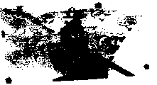
Fig. 5 has shown 9 1cm in bulk of a row
2The photo of the flexible OLED of vacuum-deposited non-polymer.Show be a device contact with detector arm in the good room that throws light at video display brightness (~100cd/m normally
2) aerial running down.
Now explain the present invention with particularly preferred embodiment of the present invention, should be understood that these embodiments as just illustrative embodiment, the present invention is not limited thereto.
As illustrative embodiment of the present invention, described OLED can introduce single assorted structure or two assorted structure.Material, the method and apparatus of the single and two assorted structures of preparation for example are disclosed in US patent No.5, in 554,220, all introduce references at this.The present invention place like this openly can be used with the following application that suspends altogether; " high reliability, efficient, organic light emitting apparatus and production method thereof that can be integrated "; " multi-colored led new material "; " based on the electric transmission and the luminescent layer of organic free radical "; " multicolor displaying apparatus "; " organic light emitting apparatus of burn red (LED) "; " highly efficient organic light-emitting device structure "; , each described application that suspends was altogether all submitted on December 23rd, 1996, all introduced reference at this.The present invention also can use with the following application that suspends altogether: U.S. series number 08/354,674; 08/613,207; 08/632,316; 08/632,322 and 08/693,359, also it is all introduced reference at this.
Here alleged list or two assorted structure just represent as shown in the Examples how the OLED that assembles by the present invention makes, and certain order of each layer shown in limiting the invention to never in any form make or order.For example, the OLED of the single assorted structure of the present invention comprises a flexible matrix, and is preferably transparent; First electrode is generally indium tin oxide (ITO) anode layer; Hole transmission layer; Electron transfer layer; Second electrode layer, for example: the metallic cathode layer of Mg:Ag; And a metal protection layer, for example make by one deck Ag, be used to protect the Mg:Ag cathode layer not to be subjected to atmospheric oxidn.Two assorted structures also comprise an other layer that contains emissive material.This extra play referred to herein as " emission layer separately " so that come with other layer difference, is because hole transmission layer and electron transfer layer can produce electroluminescence and not need this independent emission layer.
Although the thickness range that is not limited to here to be drawn, ito anode layer can be about 1000 (1 =10-8cm) to thick greater than about 4000 ; About 50 of hole transmission layer are to thick greater than about 1000 ; About 50 of that layer that contain emissive material are thick to about 200 ; About 50 of electron transfer layer are thick to about 1000 ; And about 50 of each metal level are to thick greater than about 100 , if perhaps cathode layer do not prepare to become transparent, thicker on the practical work.
The vacuum-deposited ability with molecule organic material of stable electroluminescent properties that realizes the highly flexible display especially depends on following two factors.At first, the molecular link needs corresponding to the film mechanical performance that comprised among the OLED impose on structural stress in the time of tolerating bending preferably, and the second, matrix needs enough smooth evenly so that do not form mechanical defect in the process of growth or deflection.
For first factor, in fact all organic materials used in vacuum moulding machine OLED all are fixed together by highly flexible Van der Waals key.In the past Y.Zhang and S.R.Forrest shown in the physical evaluation periodical 71,2765 (1993) (Phys, Rev Lett.71,2765 (1993)) with OLED in the bonding of used these similar aromatic molecules be highly compressible.For example: shown high about 20 times of the most of ductile metals of compression ratio of naphthyl molecular crystalline NTCDA of Van der Waals bonding such as In or Al, C.Kittel, solid-state physics (Solid State Physics) the 4th edition.(Wiley, New York, 1971) P.143.But do not really want to be confined to this theory with why the present invention can produce stable electroluminescence, what molecular material disclosed herein is this opinion can help to be interpreted as has enough ductility to remove to bear very big stress and do not ftracture.
Second factor, promptly matrix used enough smooth, be to determine by the image that uses atomic force microscope to produce.As shown in Figure 4, these images show that all sides (rms) roughness that the ITO surface has only is 1.8nm, and flexible surface of polyester is then somewhat coarse, and the rms value is 2.8nm.Although different between matrix and the matrix, the ITO surface roughness is no more than 3.6nm.All enough smooth (height that is surface topography is the very little part of device gross thickness) of matrix be not so that the assorted structure of OLED of the present invention observes tangible infringement when growth or bending in both cases.
Based on as above considering, found the device of the present invention that on flexible matrix, increases with conventional in the comparable efficient of the vacuum-deposited OLED of growth on glass and find also that in addition this device is more durable in mechanical aspects.
Describe the relevant demonstration of the present invention now in detail and how to make its specific representational especially embodiment, material, equipment and method step are appreciated that the embodiment for only being used to illustrate.Especially, the present invention's method of being not intended to be limited to quote especially, material, condition, machined parameters, equipment etc. at this.
Embodiment:
On the cross section of the preferred embodiment of the invention shown in Figure 1, the flexible matrix 2 of device is made up of any suitable flexomer sheet material such as polyester.It is 0.5cm or following that preferred this flexible matrix can be bent to radius of curvature.Flexible matrix 2 precoatings one indium tin oxide, the film 4 of ITO.As can be by Southwall Technologies., Inc., (1029 Corporation Way, Palo Alto, Calif., 94303, Part No.903-6011) buys.In this embodiment preferred, hole transmission layer 6 is by N, N '-diphenyl-N, and N '-two (3-aminomethyl phenyl)-1,1 '-biphenyl-4,4 '-diamines (TPD) is formed, and electron transfer layer 8 is by three-(oxine) aluminium (Alq
3) form.Also can use other non-polymer material, such as the material that is used to prepare hole transmission layer, electron transfer layer and emission layer known in the art.The pre-portion of the ITO layer 4 that TPD hole-conductive layer 6 is injected in the hole forms Alq
3Luminescent layer 8 forms on layer 6.Also available in addition individual layer replaces wherein TPD and Alq
3In conjunction with the layer 6 and 8.Mg-Ag layer 10 is at Alq
3Form on the layer 8, Ag layer 12 forms on Mg-Ag layer 10.Power supply 14 is connected between the ITO layer 4 of Ag layer 12 and pre-coated.
Although each layer can have and the different thickness shown in the following table, shown thickness has produced the characteristic that curve chart proved by Fig. 2 and 3.
Level numberLayer thickness
Layer 2 175uM
Layer 6 800
Layer 8 800
Layer 12 500
According to other aspects of the invention, the light-emitting device of Fig. 1 can be made as follows.In this embodiment, matrix 2 is the thick (1uM=10 of a 175uM
-6Rice) with the transparent polyester plate of transparent electroconductive ITO film 4 pre-coated.The thickness of flexible matrix can be thick or thin according to the needs of the used special application of OLED.The resistance of this ito thin film is 60 Ω/, and the transparency of coating matrix be~80% to see through visible spectrum, before organic membrane deposits, with matrix 2 ultrasonic cleaning 2 minutes in washing agent, uses rinsed with deionized water then.Then, rinsing in the 2-propyl alcohol kept 2-3 minute under the room temperature.In the 2-propyl alcohol, boiled 2-3 minute then, then carry out drying with crossing the drying nitrogen stream that filters with spray gun.By thermal evaporation<4 * 10
-7The thick hole-conductive material TPD layer 6 of deposition 800 then deposits the thick Alq of 800 in the vacuum of Torr
3Layer.Top electrodes is made up of by the thick Ag cover of 500 of shadow mask deposition the thick Mg-Ag layer and of 1500 .The conventional equipment that is manufactured on simultaneously with identical cleaning and deposition program on the glass basis of ITO pre-coated compares.The transparency of the resistance of plate and ITO pre-coated glass basis is respectively 20 Ω/ and~90%.
The flexible device that Fig. 2 a has shown the 1mm diameter before crooked (curve 16), alternating bending (4-5 time) to one than small curvature radius (~0.5cm) afterwards (curve 18) reaches the electric current-voltage characteristic of the conventional equipment (curve 20) on glass basis.All current/voltage curves show that all electric current follows power law to the dependence of voltage.Under low-voltage, the behavior of current/voltage curve display ohm; And under high voltage, curve is followed I ≈ V
M+1, m=7 is hinting that limitting the trap conduction is the feature of OLED.In changing, at least 4 grades of size of current of high voltage region can be observed power law.Current/voltage characteristic does not have obvious variation after installing deflection repeatedly.Article three, the threshold voltage of curve (being defined as electric current that the electric current that produced by ohm and the conduction of limit trap the produce voltage when equal) almost be identical (~6.5V), and leakage current even also little than conventional equipment of flexible device under low-voltage, and do not increase after crooked.To such an extent as to this show the ITO film of precoating on the flexible matrix be enough uniformly crooked after electric current shunting circuit between top and bottom contact-making surface 12 and 4 do not reduce, even for extremely thin film (~1600 molecule organic structure).
Flexible device is seen the curve 22 of Fig. 3 in optical output power-electric current (L-I) characteristic of crooked front and back and conventional equipment.Curve 24 has illustrated the L-I output of the standard set-up with glass basis.The external quantum efficiency of flexible device is 0.20%, and the external quantum efficiency of conventional equipment is 0.14%.Efficient all is that the light that is only sent by anterior scattering direction calculates in both cases.This has underestimated real quantum efficiency but to two kinds of devices relatively of great use widely.Begin the beguine, the quantum efficiency that has confirmed flexible device is not subjected to the influence of alternating bending.I-V or L-I characteristic do not have the fact of significant change to show not by bending the obvious influence of ITO contact-making surface, each organic layer and alloy top contact-making surface after the device deflection, even are reaching under the situation of very little radius of curvature.
Large tracts of land (~1cm
2) the also available similar method manufacturing of device.Identical with the situation in dingus, large-area devices also is flexible to curvature~0.5cm and tangible degraded do not occur.These large-area devices the situation that can reach show that flexible OLED can be used for large-scale, collapsible or suitable flat-panel monitor.This shows that together with ITO pre-coated matrix feasible fact in big short tube the display flexible, that OLED is basic can be basic a large amount of the manufacturing by adopting suitable volume growth technology such as organic gas deposition to do in order to roller-roller.
Failure mode to large-area devices is also studied.If at the convex surface of crooked matrix, even in polyester film, produced after the permanent crease device and also can be bent and do not have destruction.If at concave surface, when being bent to the radius of curvature of 0.5cm, still keep running property.When littler radius, crackle passes the device diffusion, produces between bottom and top contact-making surface at further crooked after-current shunting route.When the matrix of ITO pre-coated is done similar bending, also observed identical seminess, the deducibility crackle occurs among the ITO rather than occurs among the OLED self thus.
In a word, vacuum-deposited, Van der Waals bonding, the flexible OLED of non-polymer as shown in Figure 5, makes as matrix with the transparent polyester film of ITO pre-coated.It shows that ito thin film works as precoating when being applied on the flexible matrix, and be suitable for that OLED uses smooth, highly transparent, conduction, flexible contact-making surface can be provided.The OLED of the emission layer that the ITO coating matrix that this hole is injected also can be formed with the hole transport that comprises polymer, electric transmission and/or by polymer uses.In addition, be similar to performance disclosed herein if the device vacuum moulding machine of non-polymer injects in polymer, transparent hole to be expected to obtain on contact-making surface such as the polyaniline, if this in application-specific, require higher flexible also be useful.
Although the preferred OLED structure of Fig. 1 is described, should be understood that any OLED structure with layer of vacuum formation all can form on flexomer matrix of the present invention.The person skilled in the art can recognize each embodiment of the present invention is carried out certain change, and this change means by the spirit and scope of claims and covers.
Claims (25)
1. method for preparing flexible organic light emitting device comprises:
The flexible matrix that first electrode is arranged above one is provided, and described first electrode is made of the indium tin oxide that surface roughness is no more than 3.6nm;
Organic small molecule material layer of deposition on described first electrode;
One second electrode of deposition on described organic small molecule material layer.
2. method for preparing flexible organic light emitting device comprises:
A flexible matrix that is coated with indium tin oxide layer is provided, and wherein the surface roughness of indium tin oxide layer is no more than 3.6nm;
Layer that constitutes by the non-polymer organic material of deposition on described indium tin oxide layer; With
On described indium tin oxide layer described by the non-polymer organic material constitute the layer on the deposition electrode layer.
3. according to the process of claim 1 wherein that organic small molecule material is a kind of hole mobile material and the step that also is included in an organic molecule electron transport material layer of deposition above the organic molecule hole mobile material.
4. according to the method for claim 3, also be included in a kind of organic molecule emissive material of deposition between hole mobile material and the electron transport material.
5. according to the method for claim 1 or 2, wherein said flexible matrix is made of a kind of polyester matrix.
6. method for preparing flexible organic light emitting device comprises:
A flexible polyester matrix that is coated with indium tin oxide layer is provided, and wherein the surface roughness of indium tin oxide layer is no more than 3.6nm;
N of deposition on described indium tin oxide anode layer, N '-diphenyl-N, N '-two (3-aminomethyl phenyl)-1,1 '-biphenyl-4,4 '-diamines layer;
At described N, N '-diphenyl-N, N '-two (3-aminomethyl phenyl)-1,1 '-biphenyl-4,4 '-one three-(oxine) aluminium lamination of deposition above the diamines layer; With
Deposit a metal level above the aluminium lamination described three-(oxine).
7. method for preparing flexible organic light emitting device comprises:
A flexible matrix that is coated with indium tin oxide layer is provided;
Hole transmission layer that constitutes by the non-polymer organic material of vacuum moulding machine on described indium tin oxide layer;
Wherein indium tin oxide layer is enough uniform, makes when device is crooked with respect to the current-voltage of device before crooked or light-current characteristics not obviously current-voltage of modifier or light-current characteristics.
8. according to the method for claim 7, wherein the manufacturing of organic light emitting apparatus is included in the step of the electron transfer layer that one of vacuum moulding machine above the hole transmission layer is made of the non-polymer organic material.
9. method according to Claim 8, wherein the manufacturing of organic light emitting apparatus is included in the independent emission layer that one of deposition above the hole transmission layer is made up of the non-polymer organic material and the step of vacuum moulding machine electron transfer layer afterwards.
10. method for preparing flexible organic light emitting device comprises:
A flexible matrix that is coated with indium tin oxide layer is provided;
Hole transmission layer that constitutes by the non-polymer organic material of deposition on described indium tin oxide layer;
Electron transfer layer that constitutes by the non-polymer organic material of deposition on described hole transmission layer; With
Cathode layer of deposition on described electron transfer layer;
Wherein indium tin oxide layer is enough uniform, makes when device is crooked with respect to the current-voltage of device before crooked or light-current characteristics not obviously current-voltage of modifier or light-current characteristics.
11., also be included in above the hole transmission layer independent emission layer that one of deposition is made up of the non-polymer organic material and the step that on hole transmission layer, deposits electron transfer layer afterwards according to the method for claim 10.
12. according to the method for claim 11, when wherein device bends to radius of curvature 0.5cm with respect to electric current one voltage of device before crooked or light-current characteristics not obviously current-voltage of modifier or light-current characteristics.
13. according to each method of claim 7-11, wherein flexible matrix is made up of polyester matrix.
14. a flexible organic light emitting device comprises:
A flexible matrix;
Be positioned at first electrode of being made up of ito thin film of flexible substrates, the surface roughness of ITO is no more than 3.6nm;
First organic layer of forming by the non-polymer organic layer that is positioned at above first electrode;
Second electrode that is positioned at above the first non-polymer organic material.
15. a flexible organic light emitting device comprises:
A flexible matrix;
First electrode of forming by ito thin film that is positioned at flexible substrates;
First organic layer of forming by the non-polymer organic layer that is positioned at above first electrode;
Second electrode that is positioned at above the first non-polymer organic material;
Wherein indium tin oxide layer is enough uniform, makes when device is crooked with respect to the current-voltage of device before crooked or light-current characteristics not obviously current-voltage of modifier or light-current characteristics.
16. according to the device of claim 15, when wherein device bends to radius of curvature 0.5cm with respect to electric current one voltage of device before crooked or light-current characteristics not obviously current-voltage of modifier or light-current characteristics.
17. according to each device of claim 14-16, wherein first organic layer is made of hole transmission layer.
18. according to the device of claim 17, also comprise second a non-polymer organic layer between first organic layer and second electrode, wherein the second non-polymer organic layer is an electron transfer layer.
19. according to the device of claim 18, also comprise the 3rd a non-polymer organic layer between the first and second non-polymer organic layers, wherein the 3rd non-polymer organic layer is an independent emission layer.
20. according to each device of claim 14-16, wherein flexible matrix is made up of the flexomer matrix.
21. according to the device of claim 20, wherein the flexomer matrix is made up of flexible polyester matrix.
22. according to each device of claim 14-16, wherein the first non-polymer organic layer is by N, N '-diphenyl-N, and N '-two (3-aminomethyl phenyl)-1,1 '-biphenyl-4,4 '-diamines is formed.
23. according to each device of claim 14-16, wherein first electrode is an anode.
24. according to each device of claim 14-16, wherein the first non-polymer organic layer is through vacuum-deposited.
25. a display has been introduced each the device according to claim 14-24.
Applications Claiming Priority (4)
| Application Number | Priority Date | Filing Date | Title |
|---|---|---|---|
| US2400196P | 1996-08-12 | 1996-08-12 | |
| US60/024,001 | 1996-08-12 | ||
| US08/789,319 | 1997-01-23 | ||
| US08/789,319 US5844363A (en) | 1997-01-23 | 1997-01-23 | Vacuum deposited, non-polymeric flexible organic light emitting devices |
Publications (2)
| Publication Number | Publication Date |
|---|---|
| CN1230288A CN1230288A (en) | 1999-09-29 |
| CN1134039C true CN1134039C (en) | 2004-01-07 |
Family
ID=26697900
Family Applications (1)
| Application Number | Title | Priority Date | Filing Date |
|---|---|---|---|
| CNB971979022A Expired - Lifetime CN1134039C (en) | 1996-08-12 | 1997-07-30 | Non-polymeric flexible organic light emitting device |
Country Status (12)
| Country | Link |
|---|---|
| US (3) | US6602540B2 (en) |
| EP (1) | EP0946958B1 (en) |
| JP (5) | JP2000516761A (en) |
| KR (1) | KR100462723B1 (en) |
| CN (1) | CN1134039C (en) |
| AT (1) | ATE320085T1 (en) |
| AU (1) | AU4048897A (en) |
| BR (1) | BR9711155B1 (en) |
| CA (1) | CA2263150C (en) |
| DE (1) | DE69735425T2 (en) |
| HK (1) | HK1022044A1 (en) |
| WO (1) | WO1998007173A1 (en) |
Families Citing this family (90)
| Publication number | Priority date | Publication date | Assignee | Title |
|---|---|---|---|---|
| JPH11251067A (en) * | 1998-03-02 | 1999-09-17 | Junji Kido | Organic electroluminescence element |
| GB9813326D0 (en) * | 1998-06-19 | 1998-08-19 | Cambridge Display Tech Ltd | Backlit displays |
| KR100683050B1 (en) * | 1999-06-28 | 2007-02-15 | 모토로라 인코포레이티드 | Organic electroluminescent device |
| JP2003517183A (en) * | 1999-12-17 | 2003-05-20 | インスティチュート オブ マテリアルズ リサーチ アンド エンジニアリング | Transparent electrode material improved to improve the quality of OLED devices |
| EP1420975A1 (en) * | 2001-08-31 | 2004-05-26 | Johnson Controls Technology Company | Conformable vehicle display |
| JP2003133068A (en) | 2001-10-25 | 2003-05-09 | Nec Corp | Method for manufacturing luminescent display device and device for manufacturing luminescent display device by applying it |
| GB0127581D0 (en) * | 2001-11-17 | 2002-01-09 | Univ St Andrews | Therapeutic Light-emitting device |
| US7050835B2 (en) * | 2001-12-12 | 2006-05-23 | Universal Display Corporation | Intelligent multi-media display communication system |
| US20040135160A1 (en) * | 2003-01-10 | 2004-07-15 | Eastman Kodak Company | OLED device |
| US7465678B2 (en) * | 2003-03-28 | 2008-12-16 | The Trustees Of Princeton University | Deformable organic devices |
| US20050227389A1 (en) * | 2004-04-13 | 2005-10-13 | Rabin Bhattacharya | Deformable organic devices |
| CN100426556C (en) * | 2003-07-25 | 2008-10-15 | 清华大学 | Single layer organic electro luminuous device |
| JP4168968B2 (en) * | 2004-04-26 | 2008-10-22 | セイコーエプソン株式会社 | Manufacturing method of organic EL device |
| US7154114B2 (en) * | 2004-05-18 | 2006-12-26 | Universal Display Corporation | Cyclometallated iridium carbene complexes for use as hosts |
| US7393599B2 (en) * | 2004-05-18 | 2008-07-01 | The University Of Southern California | Luminescent compounds with carbene ligands |
| US7445855B2 (en) * | 2004-05-18 | 2008-11-04 | The University Of Southern California | Cationic metal-carbene complexes |
| US7582365B2 (en) * | 2005-01-10 | 2009-09-01 | Universal Display Corporation | Reversibly reducible metal complexes as electron transporting materials for OLEDs |
| US7279704B2 (en) | 2004-05-18 | 2007-10-09 | The University Of Southern California | Complexes with tridentate ligands |
| US7601436B2 (en) | 2004-05-18 | 2009-10-13 | The University Of Southern California | Carbene metal complexes as OLED materials |
| US7598388B2 (en) * | 2004-05-18 | 2009-10-06 | The University Of Southern California | Carbene containing metal complexes as OLEDs |
| US7655323B2 (en) * | 2004-05-18 | 2010-02-02 | The University Of Southern California | OLEDs utilizing macrocyclic ligand systems |
| US7534505B2 (en) * | 2004-05-18 | 2009-05-19 | The University Of Southern California | Organometallic compounds for use in electroluminescent devices |
| US7491823B2 (en) * | 2004-05-18 | 2009-02-17 | The University Of Southern California | Luminescent compounds with carbene ligands |
| US20060008670A1 (en) * | 2004-07-06 | 2006-01-12 | Chun Lin | Organic light emitting materials and devices |
| US7709100B2 (en) | 2004-07-07 | 2010-05-04 | Universal Display Corporation | Electroluminescent efficiency |
| TWI399421B (en) | 2004-07-07 | 2013-06-21 | Universal Display Corp | Stable and efficient electroluminescent materials |
| US20060008671A1 (en) * | 2004-07-07 | 2006-01-12 | Raymond Kwong | Electroluminescent efficiency |
| KR100607520B1 (en) * | 2004-11-11 | 2006-08-02 | 엘지전자 주식회사 | Organic Electro Luminescence Display Device And Fabricating Method Thereof |
| DE102004054893A1 (en) * | 2004-11-12 | 2006-05-24 | Micronas Gmbh | Method and circuit arrangement for channel filtering analog or digitally modulated TV signals |
| US7776456B2 (en) * | 2004-12-03 | 2010-08-17 | Universal Display Corporation | Organic light emitting devices with an emissive region having emissive and non-emissive layers and method of making |
| US7683536B2 (en) * | 2005-03-31 | 2010-03-23 | The Trustees Of Princeton University | OLEDs utilizing direct injection to the triplet state |
| US20060251921A1 (en) * | 2005-05-06 | 2006-11-09 | Stephen Forrest | OLEDs utilizing direct injection to the triplet state |
| US20060222886A1 (en) * | 2005-04-04 | 2006-10-05 | Raymond Kwong | Arylpyrene compounds |
| US9070884B2 (en) * | 2005-04-13 | 2015-06-30 | Universal Display Corporation | Hybrid OLED having phosphorescent and fluorescent emitters |
| US7807275B2 (en) | 2005-04-21 | 2010-10-05 | Universal Display Corporation | Non-blocked phosphorescent OLEDs |
| US9051344B2 (en) | 2005-05-06 | 2015-06-09 | Universal Display Corporation | Stability OLED materials and devices |
| US7902374B2 (en) * | 2005-05-06 | 2011-03-08 | Universal Display Corporation | Stability OLED materials and devices |
| US7851072B2 (en) * | 2005-05-19 | 2010-12-14 | Universal Display Corporation | Stable and efficient electroluminescent materials |
| EP2277978B1 (en) | 2005-05-31 | 2016-03-30 | Universal Display Corporation | Triphenylene hosts in phosphorescent light emitting diodes |
| US7474048B2 (en) * | 2005-06-01 | 2009-01-06 | The Trustees Of Princeton University | Fluorescent filtered electrophosphorescence |
| US8148891B2 (en) * | 2005-10-04 | 2012-04-03 | Universal Display Corporation | Electron impeding layer for high efficiency phosphorescent OLEDs |
| US20070103066A1 (en) * | 2005-11-04 | 2007-05-10 | D Andrade Brian W | Stacked OLEDs with a reflective conductive layer |
| US8021763B2 (en) | 2005-11-23 | 2011-09-20 | The Trustees Of Princeton University | Phosphorescent OLED with interlayer |
| EP3569606B1 (en) | 2006-02-10 | 2022-01-05 | Universal Display Corporation | Metal complexes of cyclometallated imidazo (1,2-f)phenanthridine and diimidazo (1,2-a; 1', 2'-c)quinazoline ligands and isoelectronic and benzannulated analogs thereof |
| US8142909B2 (en) * | 2006-02-10 | 2012-03-27 | Universal Display Corporation | Blue phosphorescent imidazophenanthridine materials |
| KR101617443B1 (en) | 2006-04-13 | 2016-05-02 | 유니버시티 오브 써던 캘리포니아 | Organic electronic devices using phthalimide compounds |
| US7579773B2 (en) * | 2006-06-05 | 2009-08-25 | The Trustees Of Princeton University | Organic light-emitting device with a phosphor-sensitized fluorescent emission layer |
| US20080007936A1 (en) * | 2006-07-05 | 2008-01-10 | Jie Liu | Organic illumination source and method for controlled illumination |
| CA2658578A1 (en) | 2006-07-18 | 2008-09-04 | The University Of Southern California | Organic optoelectronic device electrodes with nanotubes |
| US7724796B2 (en) * | 2006-08-29 | 2010-05-25 | The Trustees Of Princeton University | Organic laser |
| US7710017B2 (en) * | 2006-09-08 | 2010-05-04 | Universal Display Corporation | Organic light emitting device having a transparent microcavity |
| US7598381B2 (en) | 2006-09-11 | 2009-10-06 | The Trustees Of Princeton University | Near-infrared emitting organic compounds and organic devices using the same |
| US7800295B2 (en) * | 2006-09-15 | 2010-09-21 | Universal Display Corporation | Organic light emitting device having a microcavity |
| US8945722B2 (en) * | 2006-10-27 | 2015-02-03 | The University Of Southern California | Materials and architectures for efficient harvesting of singlet and triplet excitons for white light emitting OLEDs |
| EP2439806B1 (en) | 2007-03-30 | 2014-01-15 | The Regents of the University of Michigan | OLED with improved light outcoupling |
| US7993763B2 (en) * | 2007-05-10 | 2011-08-09 | Universal Display Corporation | Organometallic compounds having host and dopant functionalities |
| CN101808964B (en) | 2007-08-08 | 2014-01-01 | 通用显示公司 | Single triphenylene [9,10] chromophores in phosphorescent light emitting diodes |
| US8383249B2 (en) * | 2007-10-04 | 2013-02-26 | Universal Display Corporation | Complexes with tridentate ligands |
| US8067100B2 (en) * | 2007-10-04 | 2011-11-29 | Universal Display Corporation | Complexes with tridentate ligands |
| KR101522735B1 (en) * | 2008-09-03 | 2015-05-26 | 엘지전자 주식회사 | Portable terminal |
| KR101804084B1 (en) * | 2008-09-25 | 2017-12-01 | 유니버셜 디스플레이 코포레이션 | Organoselenium materials and their uses in organic light emitting devices |
| US8766291B2 (en) | 2008-10-28 | 2014-07-01 | The Regents Of The University Of Michigan | Stacked white OLED having separate red, green and blue sub-elements |
| WO2010149259A2 (en) * | 2009-06-22 | 2010-12-29 | Merck Patent Gmbh | Conducting formulation |
| US8581262B2 (en) | 2009-08-04 | 2013-11-12 | Merck Patent Gmbh | Electronic devices comprising multi cyclic hydrocarbons |
| KR101084230B1 (en) * | 2009-11-16 | 2011-11-16 | 삼성모바일디스플레이주식회사 | Organic light emitting diode display and method for manufacturing the same |
| EP2517275B1 (en) | 2009-12-22 | 2018-11-07 | Merck Patent GmbH | Formulations comprising phase-separated functional materials |
| WO2011076314A1 (en) | 2009-12-22 | 2011-06-30 | Merck Patent Gmbh | Electroluminescent formulations |
| JP5897472B2 (en) | 2009-12-22 | 2016-03-30 | メルク パテント ゲーエムベーハー | Electroluminescent functional surfactant |
| KR20190018049A (en) * | 2010-03-08 | 2019-02-20 | 가부시키가이샤 한도오따이 에네루기 켄큐쇼 | Semiconductor device and method for manufacturing semiconductor device |
| JP6246468B2 (en) | 2010-03-11 | 2017-12-13 | メルク パテント ゲーエムベーハー | Fiber in therapy and cosmetics |
| US10190043B2 (en) | 2010-05-27 | 2019-01-29 | Merck Patent Gmbh | Compositions comprising quantum dots |
| US20120049168A1 (en) | 2010-08-31 | 2012-03-01 | Universal Display Corporation | Cross-Linked Charge Transport Layer Containing an Additive Compound |
| EP2474967A1 (en) * | 2011-01-06 | 2012-07-11 | Koninklijke Philips Electronics N.V. | Luminescent-OLED light collector signage panel |
| JP2011091063A (en) * | 2011-02-09 | 2011-05-06 | Inst Of Materials Research & Engineering | Transparent electrode material which is improved for improvement of performance of oled device |
| JP5355618B2 (en) | 2011-03-10 | 2013-11-27 | 三星ディスプレイ株式會社 | Flexible display device and manufacturing method thereof |
| US9023420B2 (en) | 2011-07-14 | 2015-05-05 | Universal Display Corporation | Composite organic/inorganic layer for organic light-emitting devices |
| KR101830179B1 (en) | 2011-11-03 | 2018-02-21 | 삼성디스플레이 주식회사 | Organic Light Emitting Diode Display Device |
| US9853243B2 (en) | 2013-07-05 | 2017-12-26 | Industrial Technology Research Institute | Flexible display and method for fabricating the same |
| TWI583947B (en) * | 2013-12-16 | 2017-05-21 | 聖高拜塑膠製品公司 | Electrode and method for making an electrode |
| US9666822B2 (en) | 2013-12-17 | 2017-05-30 | The Regents Of The University Of Michigan | Extended OLED operational lifetime through phosphorescent dopant profile management |
| JP5723046B2 (en) * | 2014-06-27 | 2015-05-27 | 日東電工株式会社 | Organic EL device manufacturing method and organic EL device |
| JP2014209493A (en) * | 2014-06-27 | 2014-11-06 | 日東電工株式会社 | Method of manufacturing organic el device, and organic el device |
| US10818853B2 (en) | 2015-06-04 | 2020-10-27 | University Of Southern California | Organic electroluminescent materials and devices |
| DE102016009067A1 (en) | 2016-07-27 | 2018-02-15 | Docter Optics Se | Headlight lens for a motor vehicle headlight |
| CN110088609A (en) | 2016-11-30 | 2019-08-02 | 美国圣戈班性能塑料公司 | Electrode and electrode manufacturing method |
| CN106654066A (en) * | 2017-01-06 | 2017-05-10 | 京东方科技集团股份有限公司 | Manufacturing method of OLED device |
| KR102369676B1 (en) | 2017-04-10 | 2022-03-04 | 삼성디스플레이 주식회사 | Apparatus and method for manufacturing a display apparatus |
| KR20230002860A (en) | 2020-04-21 | 2023-01-05 | 메르크 파텐트 게엠베하 | Emulsion containing organic functional materials |
| WO2023012084A1 (en) | 2021-08-02 | 2023-02-09 | Merck Patent Gmbh | A printing method by combining inks |
| TW202411366A (en) | 2022-06-07 | 2024-03-16 | 德商麥克專利有限公司 | Method of printing a functional layer of an electronic device by combining inks |
Family Cites Families (38)
| Publication number | Priority date | Publication date | Assignee | Title |
|---|---|---|---|---|
| US4020389A (en) * | 1976-04-05 | 1977-04-26 | Minnesota Mining And Manufacturing Company | Electrode construction for flexible electroluminescent lamp |
| US4194022A (en) * | 1977-07-25 | 1980-03-18 | Ppg Industries, Inc. | Transparent, colorless, electrically conductive coating |
| JPS5856479A (en) * | 1981-09-30 | 1983-04-04 | Hoya Corp | Substrate for electrode |
| US4786570A (en) | 1987-04-21 | 1988-11-22 | Xerox Corporation | Layered, flexible electrophotographic imaging member having hole blocking and adhesive layers |
| JPH02106891A (en) * | 1988-10-13 | 1990-04-18 | Nec Kansai Ltd | Manufacture of electric field luminous lamp |
| US4943508A (en) | 1989-07-03 | 1990-07-24 | Xerox Corporation | Method of fabricating a layered flexible electrophotographic imaging member |
| JP2774351B2 (en) * | 1990-03-26 | 1998-07-09 | 出光興産株式会社 | Organic thin-film electroluminescence device and method of manufacturing the same |
| US5364654A (en) * | 1990-06-14 | 1994-11-15 | Idemitsu Kosan Co., Ltd. | Process for production of a thin film electrode and an electroluminescence device |
| US5331182A (en) * | 1990-08-08 | 1994-07-19 | Matsushita Electric Industrial Co., Ltd. | Organic light emitting device and preparation and use thereof |
| JPH056491U (en) * | 1991-07-09 | 1993-01-29 | 株式会社ヤマウ | EL lighting device |
| US5389444A (en) * | 1991-09-18 | 1995-02-14 | Idemitsu Kosan Co., Ltd. | Organic electroluminescence device |
| JPH0594875A (en) * | 1991-09-30 | 1993-04-16 | Toppan Printing Co Ltd | Organic thin-film el element |
| JP3341086B2 (en) * | 1991-12-11 | 2002-11-05 | 株式会社リコー | EL device |
| US5652067A (en) * | 1992-09-10 | 1997-07-29 | Toppan Printing Co., Ltd. | Organic electroluminescent device |
| JPH06124785A (en) * | 1992-10-08 | 1994-05-06 | Idemitsu Kosan Co Ltd | Organic el element |
| JPH06267658A (en) * | 1993-03-09 | 1994-09-22 | Mitsubishi Kasei Corp | Organic el element |
| JP3266361B2 (en) * | 1993-04-06 | 2002-03-18 | 日本電信電話株式会社 | Manufacturing method of reflector |
| JP3224459B2 (en) * | 1993-09-10 | 2001-10-29 | 出光興産株式会社 | Organic EL element and organic EL display |
| JP3273389B2 (en) * | 1993-10-13 | 2002-04-08 | 株式会社リコー | EL device |
| US5597890A (en) * | 1993-11-01 | 1997-01-28 | Research Corporation Technologies, Inc. | Conjugated polymer exciplexes and applications thereof |
| US5482896A (en) | 1993-11-18 | 1996-01-09 | Eastman Kodak Company | Light emitting device comprising an organic LED array on an ultra thin substrate and process for forming same |
| WO1995031831A1 (en) | 1994-05-18 | 1995-11-23 | Philips Electronics N.V. | Method of providing a film of conjugated, substituted or unsubstituted poly(p-phenylene vinylene) on a substrate by chemical vapour deposition (cvd), as well as a method of manufacturing an electroluminescent (el) device |
| US5558904A (en) * | 1994-07-08 | 1996-09-24 | Xerox Corporation | Electroluminescent devices containing a conjugated polymer obtained via halogen precursor route chemistry |
| DE69529512T2 (en) * | 1994-09-06 | 2003-11-13 | Koninklijke Philips Electronics N.V., Eindhoven | Electroluminescent device with a poly-3,4-ethylene-dioxythiophene layer |
| JPH08124679A (en) * | 1994-10-25 | 1996-05-17 | Ibm Japan Ltd | Electroluminescent device |
| US5703436A (en) * | 1994-12-13 | 1997-12-30 | The Trustees Of Princeton University | Transparent contacts for organic devices |
| US5707745A (en) * | 1994-12-13 | 1998-01-13 | The Trustees Of Princeton University | Multicolor organic light emitting devices |
| US6358631B1 (en) * | 1994-12-13 | 2002-03-19 | The Trustees Of Princeton University | Mixed vapor deposited films for electroluminescent devices |
| JP3586906B2 (en) * | 1994-12-14 | 2004-11-10 | 凸版印刷株式会社 | Method for manufacturing transparent conductive film |
| JPH08199161A (en) * | 1995-01-26 | 1996-08-06 | Mitsubishi Chem Corp | Organic electroluminescence element |
| US5554220A (en) | 1995-05-19 | 1996-09-10 | The Trustees Of Princeton University | Method and apparatus using organic vapor phase deposition for the growth of organic thin films with large optical non-linearities |
| US5719467A (en) * | 1995-07-27 | 1998-02-17 | Hewlett-Packard Company | Organic electroluminescent device |
| US6048630A (en) * | 1996-07-02 | 2000-04-11 | The Trustees Of Princeton University | Red-emitting organic light emitting devices (OLED's) |
| US5714838A (en) * | 1996-09-20 | 1998-02-03 | International Business Machines Corporation | Optically transparent diffusion barrier and top electrode in organic light emitting diode structures |
| US6013982A (en) | 1996-12-23 | 2000-01-11 | The Trustees Of Princeton University | Multicolor display devices |
| US6046543A (en) * | 1996-12-23 | 2000-04-04 | The Trustees Of Princeton University | High reliability, high efficiency, integratable organic light emitting devices and methods of producing same |
| US5834893A (en) * | 1996-12-23 | 1998-11-10 | The Trustees Of Princeton University | High efficiency organic light emitting devices with light directing structures |
| US5811833A (en) * | 1996-12-23 | 1998-09-22 | University Of So. Ca | Electron transporting and light emitting layers based on organic free radicals |
-
1997
- 1997-07-30 AT AT97938075T patent/ATE320085T1/en not_active IP Right Cessation
- 1997-07-30 KR KR10-1999-7001235A patent/KR100462723B1/en not_active IP Right Cessation
- 1997-07-30 WO PCT/US1997/013451 patent/WO1998007173A1/en active IP Right Grant
- 1997-07-30 DE DE69735425T patent/DE69735425T2/en not_active Expired - Lifetime
- 1997-07-30 EP EP97938075A patent/EP0946958B1/en not_active Expired - Lifetime
- 1997-07-30 AU AU40488/97A patent/AU4048897A/en not_active Abandoned
- 1997-07-30 CA CA002263150A patent/CA2263150C/en not_active Expired - Lifetime
- 1997-07-30 CN CNB971979022A patent/CN1134039C/en not_active Expired - Lifetime
- 1997-07-30 JP JP10509779A patent/JP2000516761A/en active Pending
- 1997-07-30 BR BRPI9711155-4A patent/BR9711155B1/en not_active IP Right Cessation
- 1997-10-27 US US08/957,909 patent/US6602540B2/en not_active Expired - Lifetime
-
2000
- 2000-02-14 HK HK00100868A patent/HK1022044A1/en not_active IP Right Cessation
-
2003
- 2003-05-14 US US10/437,051 patent/US6888306B2/en not_active Expired - Lifetime
-
2004
- 2004-10-15 US US10/966,417 patent/US7247073B2/en not_active Expired - Fee Related
-
2007
- 2007-03-15 JP JP2007067619A patent/JP2007242623A/en active Pending
-
2008
- 2008-11-26 JP JP2008301649A patent/JP2009111400A/en not_active Withdrawn
-
2011
- 2011-12-16 JP JP2011275676A patent/JP2012104492A/en not_active Withdrawn
-
2014
- 2014-12-04 JP JP2014245876A patent/JP2015084332A/en active Pending
Also Published As
| Publication number | Publication date |
|---|---|
| US6888306B2 (en) | 2005-05-03 |
| JP2012104492A (en) | 2012-05-31 |
| EP0946958A1 (en) | 1999-10-06 |
| DE69735425D1 (en) | 2006-05-04 |
| JP2000516761A (en) | 2000-12-12 |
| CN1230288A (en) | 1999-09-29 |
| US20050079279A1 (en) | 2005-04-14 |
| JP2015084332A (en) | 2015-04-30 |
| EP0946958A4 (en) | 2002-07-24 |
| KR100462723B1 (en) | 2004-12-20 |
| ATE320085T1 (en) | 2006-03-15 |
| BR9711155A (en) | 1999-08-17 |
| JP2009111400A (en) | 2009-05-21 |
| HK1022044A1 (en) | 2000-07-21 |
| WO1998007173A1 (en) | 1998-02-19 |
| EP0946958B1 (en) | 2006-03-08 |
| CA2263150A1 (en) | 1998-02-19 |
| JP2007242623A (en) | 2007-09-20 |
| US20040027065A1 (en) | 2004-02-12 |
| CA2263150C (en) | 2005-06-21 |
| US7247073B2 (en) | 2007-07-24 |
| AU4048897A (en) | 1998-03-06 |
| KR20000029979A (en) | 2000-05-25 |
| BR9711155B1 (en) | 2009-05-05 |
| US6602540B2 (en) | 2003-08-05 |
| US20020058103A1 (en) | 2002-05-16 |
| DE69735425T2 (en) | 2006-11-23 |
Similar Documents
| Publication | Publication Date | Title |
|---|---|---|
| CN1134039C (en) | Non-polymeric flexible organic light emitting device | |
| US5844363A (en) | Vacuum deposited, non-polymeric flexible organic light emitting devices | |
| WO1998007173A9 (en) | Non-polymeric flexible organic light emitting device | |
| KR101472963B1 (en) | A light emissive device structure and a method of fabricating the same | |
| US20040160178A1 (en) | Organic light-emitting devices and their encapsulation method and application of this method | |
| JPH0945479A (en) | Organic electroluminescence device and manufacture of organic electroluminescence device | |
| US7270894B2 (en) | Metal compound-metal multilayer electrodes for organic electronic devices | |
| JP2011524463A (en) | Conductive structure for light transmissive devices | |
| JP2008524853A (en) | Organic light-emitting diodes (OLEDs) with improved stability, brightness and efficiency | |
| US20090021161A1 (en) | Organic electroluminescent devices incorporating uv-illuminated fluorocarbon layers | |
| EP0914025A1 (en) | A multistructured electrode for use with electroluminescent devices | |
| Zhang et al. | Highly efficient organic light-emitting devices with surface-modified metal anode by vanadium pentoxide | |
| CN1156198C (en) | Flexible organic electroluminescent device | |
| KR100518420B1 (en) | Organic Electro luminescence Device and fabrication method of thereof | |
| Qiu et al. | Flexible organic light-emitting diodes with poly-3, 4-ethylenedioxythiophene as transparent anode | |
| Weaver et al. | Flexible organic LED displays | |
| Tsang | Organic light-emitting diodes fabricated on a new transparent conducting anode: aluminium-doped zinc oxide | |
| DE10137712A1 (en) | Organic electroluminescent display device with protective layer | |
| Zhu | Organic Semiconductors and Applications | |
| Anand et al. | Polymer and Small Molecules Light Emitting Diodes-A Technology for Large Area Low Information Contents Displays | |
| Burrows et al. | Organic light-emitting devices for ultralightweight color flat panel displays | |
| Jeong et al. | Influence of electrode modification by Ar+ ion beam upon passivation and electrical characteristics in organic light-emitting diodes | |
| Destruel et al. | OLEDs: a new technology for lighting and displays G. Ablart | |
| Mahmoudloo | Organic Light Emitting Diodes: Innovative Lighting and Display Solution |
Legal Events
| Date | Code | Title | Description |
|---|---|---|---|
| C06 | Publication | ||
| PB01 | Publication | ||
| C10 | Entry into substantive examination | ||
| SE01 | Entry into force of request for substantive examination | ||
| C14 | Grant of patent or utility model | ||
| GR01 | Patent grant | ||
| REG | Reference to a national code |
Ref country code: HK Ref legal event code: GR Ref document number: 1059414 Country of ref document: HK |
|
| CX01 | Expiry of patent term | ||
| CX01 | Expiry of patent term |
Granted publication date: 20040107 |