CN113215550A - Method of forming a structure, formed structure and system for forming the structure - Google Patents
Method of forming a structure, formed structure and system for forming the structure Download PDFInfo
- Publication number
- CN113215550A CN113215550A CN202110135743.XA CN202110135743A CN113215550A CN 113215550 A CN113215550 A CN 113215550A CN 202110135743 A CN202110135743 A CN 202110135743A CN 113215550 A CN113215550 A CN 113215550A
- Authority
- CN
- China
- Prior art keywords
- reaction chamber
- plasma
- carbon material
- carbon
- during
- Prior art date
- Legal status (The legal status is an assumption and is not a legal conclusion. Google has not performed a legal analysis and makes no representation as to the accuracy of the status listed.)
- Pending
Links
Images


Classifications
-
- C—CHEMISTRY; METALLURGY
- C23—COATING METALLIC MATERIAL; COATING MATERIAL WITH METALLIC MATERIAL; CHEMICAL SURFACE TREATMENT; DIFFUSION TREATMENT OF METALLIC MATERIAL; COATING BY VACUUM EVAPORATION, BY SPUTTERING, BY ION IMPLANTATION OR BY CHEMICAL VAPOUR DEPOSITION, IN GENERAL; INHIBITING CORROSION OF METALLIC MATERIAL OR INCRUSTATION IN GENERAL
- C23C—COATING METALLIC MATERIAL; COATING MATERIAL WITH METALLIC MATERIAL; SURFACE TREATMENT OF METALLIC MATERIAL BY DIFFUSION INTO THE SURFACE, BY CHEMICAL CONVERSION OR SUBSTITUTION; COATING BY VACUUM EVAPORATION, BY SPUTTERING, BY ION IMPLANTATION OR BY CHEMICAL VAPOUR DEPOSITION, IN GENERAL
- C23C16/00—Chemical coating by decomposition of gaseous compounds, without leaving reaction products of surface material in the coating, i.e. chemical vapour deposition [CVD] processes
- C23C16/22—Chemical coating by decomposition of gaseous compounds, without leaving reaction products of surface material in the coating, i.e. chemical vapour deposition [CVD] processes characterised by the deposition of inorganic material, other than metallic material
- C23C16/26—Deposition of carbon only
-
- C—CHEMISTRY; METALLURGY
- C23—COATING METALLIC MATERIAL; COATING MATERIAL WITH METALLIC MATERIAL; CHEMICAL SURFACE TREATMENT; DIFFUSION TREATMENT OF METALLIC MATERIAL; COATING BY VACUUM EVAPORATION, BY SPUTTERING, BY ION IMPLANTATION OR BY CHEMICAL VAPOUR DEPOSITION, IN GENERAL; INHIBITING CORROSION OF METALLIC MATERIAL OR INCRUSTATION IN GENERAL
- C23C—COATING METALLIC MATERIAL; COATING MATERIAL WITH METALLIC MATERIAL; SURFACE TREATMENT OF METALLIC MATERIAL BY DIFFUSION INTO THE SURFACE, BY CHEMICAL CONVERSION OR SUBSTITUTION; COATING BY VACUUM EVAPORATION, BY SPUTTERING, BY ION IMPLANTATION OR BY CHEMICAL VAPOUR DEPOSITION, IN GENERAL
- C23C16/00—Chemical coating by decomposition of gaseous compounds, without leaving reaction products of surface material in the coating, i.e. chemical vapour deposition [CVD] processes
- C23C16/44—Chemical coating by decomposition of gaseous compounds, without leaving reaction products of surface material in the coating, i.e. chemical vapour deposition [CVD] processes characterised by the method of coating
- C23C16/455—Chemical coating by decomposition of gaseous compounds, without leaving reaction products of surface material in the coating, i.e. chemical vapour deposition [CVD] processes characterised by the method of coating characterised by the method used for introducing gases into reaction chamber or for modifying gas flows in reaction chamber
- C23C16/45523—Pulsed gas flow or change of composition over time
- C23C16/45525—Atomic layer deposition [ALD]
- C23C16/45527—Atomic layer deposition [ALD] characterized by the ALD cycle, e.g. different flows or temperatures during half-reactions, unusual pulsing sequence, use of precursor mixtures or auxiliary reactants or activations
- C23C16/45536—Use of plasma, radiation or electromagnetic fields
- C23C16/45538—Plasma being used continuously during the ALD cycle
-
- C—CHEMISTRY; METALLURGY
- C23—COATING METALLIC MATERIAL; COATING MATERIAL WITH METALLIC MATERIAL; CHEMICAL SURFACE TREATMENT; DIFFUSION TREATMENT OF METALLIC MATERIAL; COATING BY VACUUM EVAPORATION, BY SPUTTERING, BY ION IMPLANTATION OR BY CHEMICAL VAPOUR DEPOSITION, IN GENERAL; INHIBITING CORROSION OF METALLIC MATERIAL OR INCRUSTATION IN GENERAL
- C23C—COATING METALLIC MATERIAL; COATING MATERIAL WITH METALLIC MATERIAL; SURFACE TREATMENT OF METALLIC MATERIAL BY DIFFUSION INTO THE SURFACE, BY CHEMICAL CONVERSION OR SUBSTITUTION; COATING BY VACUUM EVAPORATION, BY SPUTTERING, BY ION IMPLANTATION OR BY CHEMICAL VAPOUR DEPOSITION, IN GENERAL
- C23C16/00—Chemical coating by decomposition of gaseous compounds, without leaving reaction products of surface material in the coating, i.e. chemical vapour deposition [CVD] processes
- C23C16/02—Pretreatment of the material to be coated
- C23C16/0272—Deposition of sub-layers, e.g. to promote the adhesion of the main coating
-
- C—CHEMISTRY; METALLURGY
- C23—COATING METALLIC MATERIAL; COATING MATERIAL WITH METALLIC MATERIAL; CHEMICAL SURFACE TREATMENT; DIFFUSION TREATMENT OF METALLIC MATERIAL; COATING BY VACUUM EVAPORATION, BY SPUTTERING, BY ION IMPLANTATION OR BY CHEMICAL VAPOUR DEPOSITION, IN GENERAL; INHIBITING CORROSION OF METALLIC MATERIAL OR INCRUSTATION IN GENERAL
- C23C—COATING METALLIC MATERIAL; COATING MATERIAL WITH METALLIC MATERIAL; SURFACE TREATMENT OF METALLIC MATERIAL BY DIFFUSION INTO THE SURFACE, BY CHEMICAL CONVERSION OR SUBSTITUTION; COATING BY VACUUM EVAPORATION, BY SPUTTERING, BY ION IMPLANTATION OR BY CHEMICAL VAPOUR DEPOSITION, IN GENERAL
- C23C16/00—Chemical coating by decomposition of gaseous compounds, without leaving reaction products of surface material in the coating, i.e. chemical vapour deposition [CVD] processes
- C23C16/04—Coating on selected surface areas, e.g. using masks
- C23C16/045—Coating cavities or hollow spaces, e.g. interior of tubes; Infiltration of porous substrates
-
- C—CHEMISTRY; METALLURGY
- C23—COATING METALLIC MATERIAL; COATING MATERIAL WITH METALLIC MATERIAL; CHEMICAL SURFACE TREATMENT; DIFFUSION TREATMENT OF METALLIC MATERIAL; COATING BY VACUUM EVAPORATION, BY SPUTTERING, BY ION IMPLANTATION OR BY CHEMICAL VAPOUR DEPOSITION, IN GENERAL; INHIBITING CORROSION OF METALLIC MATERIAL OR INCRUSTATION IN GENERAL
- C23C—COATING METALLIC MATERIAL; COATING MATERIAL WITH METALLIC MATERIAL; SURFACE TREATMENT OF METALLIC MATERIAL BY DIFFUSION INTO THE SURFACE, BY CHEMICAL CONVERSION OR SUBSTITUTION; COATING BY VACUUM EVAPORATION, BY SPUTTERING, BY ION IMPLANTATION OR BY CHEMICAL VAPOUR DEPOSITION, IN GENERAL
- C23C16/00—Chemical coating by decomposition of gaseous compounds, without leaving reaction products of surface material in the coating, i.e. chemical vapour deposition [CVD] processes
- C23C16/44—Chemical coating by decomposition of gaseous compounds, without leaving reaction products of surface material in the coating, i.e. chemical vapour deposition [CVD] processes characterised by the method of coating
- C23C16/455—Chemical coating by decomposition of gaseous compounds, without leaving reaction products of surface material in the coating, i.e. chemical vapour deposition [CVD] processes characterised by the method of coating characterised by the method used for introducing gases into reaction chamber or for modifying gas flows in reaction chamber
- C23C16/45523—Pulsed gas flow or change of composition over time
-
- C—CHEMISTRY; METALLURGY
- C23—COATING METALLIC MATERIAL; COATING MATERIAL WITH METALLIC MATERIAL; CHEMICAL SURFACE TREATMENT; DIFFUSION TREATMENT OF METALLIC MATERIAL; COATING BY VACUUM EVAPORATION, BY SPUTTERING, BY ION IMPLANTATION OR BY CHEMICAL VAPOUR DEPOSITION, IN GENERAL; INHIBITING CORROSION OF METALLIC MATERIAL OR INCRUSTATION IN GENERAL
- C23C—COATING METALLIC MATERIAL; COATING MATERIAL WITH METALLIC MATERIAL; SURFACE TREATMENT OF METALLIC MATERIAL BY DIFFUSION INTO THE SURFACE, BY CHEMICAL CONVERSION OR SUBSTITUTION; COATING BY VACUUM EVAPORATION, BY SPUTTERING, BY ION IMPLANTATION OR BY CHEMICAL VAPOUR DEPOSITION, IN GENERAL
- C23C16/00—Chemical coating by decomposition of gaseous compounds, without leaving reaction products of surface material in the coating, i.e. chemical vapour deposition [CVD] processes
- C23C16/44—Chemical coating by decomposition of gaseous compounds, without leaving reaction products of surface material in the coating, i.e. chemical vapour deposition [CVD] processes characterised by the method of coating
- C23C16/50—Chemical coating by decomposition of gaseous compounds, without leaving reaction products of surface material in the coating, i.e. chemical vapour deposition [CVD] processes characterised by the method of coating using electric discharges
- C23C16/505—Chemical coating by decomposition of gaseous compounds, without leaving reaction products of surface material in the coating, i.e. chemical vapour deposition [CVD] processes characterised by the method of coating using electric discharges using radio frequency discharges
-
- C—CHEMISTRY; METALLURGY
- C23—COATING METALLIC MATERIAL; COATING MATERIAL WITH METALLIC MATERIAL; CHEMICAL SURFACE TREATMENT; DIFFUSION TREATMENT OF METALLIC MATERIAL; COATING BY VACUUM EVAPORATION, BY SPUTTERING, BY ION IMPLANTATION OR BY CHEMICAL VAPOUR DEPOSITION, IN GENERAL; INHIBITING CORROSION OF METALLIC MATERIAL OR INCRUSTATION IN GENERAL
- C23C—COATING METALLIC MATERIAL; COATING MATERIAL WITH METALLIC MATERIAL; SURFACE TREATMENT OF METALLIC MATERIAL BY DIFFUSION INTO THE SURFACE, BY CHEMICAL CONVERSION OR SUBSTITUTION; COATING BY VACUUM EVAPORATION, BY SPUTTERING, BY ION IMPLANTATION OR BY CHEMICAL VAPOUR DEPOSITION, IN GENERAL
- C23C16/00—Chemical coating by decomposition of gaseous compounds, without leaving reaction products of surface material in the coating, i.e. chemical vapour deposition [CVD] processes
- C23C16/44—Chemical coating by decomposition of gaseous compounds, without leaving reaction products of surface material in the coating, i.e. chemical vapour deposition [CVD] processes characterised by the method of coating
- C23C16/50—Chemical coating by decomposition of gaseous compounds, without leaving reaction products of surface material in the coating, i.e. chemical vapour deposition [CVD] processes characterised by the method of coating using electric discharges
- C23C16/515—Chemical coating by decomposition of gaseous compounds, without leaving reaction products of surface material in the coating, i.e. chemical vapour deposition [CVD] processes characterised by the method of coating using electric discharges using pulsed discharges
-
- C—CHEMISTRY; METALLURGY
- C23—COATING METALLIC MATERIAL; COATING MATERIAL WITH METALLIC MATERIAL; CHEMICAL SURFACE TREATMENT; DIFFUSION TREATMENT OF METALLIC MATERIAL; COATING BY VACUUM EVAPORATION, BY SPUTTERING, BY ION IMPLANTATION OR BY CHEMICAL VAPOUR DEPOSITION, IN GENERAL; INHIBITING CORROSION OF METALLIC MATERIAL OR INCRUSTATION IN GENERAL
- C23C—COATING METALLIC MATERIAL; COATING MATERIAL WITH METALLIC MATERIAL; SURFACE TREATMENT OF METALLIC MATERIAL BY DIFFUSION INTO THE SURFACE, BY CHEMICAL CONVERSION OR SUBSTITUTION; COATING BY VACUUM EVAPORATION, BY SPUTTERING, BY ION IMPLANTATION OR BY CHEMICAL VAPOUR DEPOSITION, IN GENERAL
- C23C16/00—Chemical coating by decomposition of gaseous compounds, without leaving reaction products of surface material in the coating, i.e. chemical vapour deposition [CVD] processes
- C23C16/44—Chemical coating by decomposition of gaseous compounds, without leaving reaction products of surface material in the coating, i.e. chemical vapour deposition [CVD] processes characterised by the method of coating
- C23C16/50—Chemical coating by decomposition of gaseous compounds, without leaving reaction products of surface material in the coating, i.e. chemical vapour deposition [CVD] processes characterised by the method of coating using electric discharges
- C23C16/517—Chemical coating by decomposition of gaseous compounds, without leaving reaction products of surface material in the coating, i.e. chemical vapour deposition [CVD] processes characterised by the method of coating using electric discharges using a combination of discharges covered by two or more of groups C23C16/503 - C23C16/515
-
- C—CHEMISTRY; METALLURGY
- C23—COATING METALLIC MATERIAL; COATING MATERIAL WITH METALLIC MATERIAL; CHEMICAL SURFACE TREATMENT; DIFFUSION TREATMENT OF METALLIC MATERIAL; COATING BY VACUUM EVAPORATION, BY SPUTTERING, BY ION IMPLANTATION OR BY CHEMICAL VAPOUR DEPOSITION, IN GENERAL; INHIBITING CORROSION OF METALLIC MATERIAL OR INCRUSTATION IN GENERAL
- C23C—COATING METALLIC MATERIAL; COATING MATERIAL WITH METALLIC MATERIAL; SURFACE TREATMENT OF METALLIC MATERIAL BY DIFFUSION INTO THE SURFACE, BY CHEMICAL CONVERSION OR SUBSTITUTION; COATING BY VACUUM EVAPORATION, BY SPUTTERING, BY ION IMPLANTATION OR BY CHEMICAL VAPOUR DEPOSITION, IN GENERAL
- C23C16/00—Chemical coating by decomposition of gaseous compounds, without leaving reaction products of surface material in the coating, i.e. chemical vapour deposition [CVD] processes
- C23C16/56—After-treatment
-
- H—ELECTRICITY
- H01—ELECTRIC ELEMENTS
- H01L—SEMICONDUCTOR DEVICES NOT COVERED BY CLASS H10
- H01L21/00—Processes or apparatus adapted for the manufacture or treatment of semiconductor or solid state devices or of parts thereof
- H01L21/02—Manufacture or treatment of semiconductor devices or of parts thereof
- H01L21/02104—Forming layers
- H01L21/02107—Forming insulating materials on a substrate
- H01L21/02109—Forming insulating materials on a substrate characterised by the type of layer, e.g. type of material, porous/non-porous, pre-cursors, mixtures or laminates
- H01L21/02112—Forming insulating materials on a substrate characterised by the type of layer, e.g. type of material, porous/non-porous, pre-cursors, mixtures or laminates characterised by the material of the layer
- H01L21/02115—Forming insulating materials on a substrate characterised by the type of layer, e.g. type of material, porous/non-porous, pre-cursors, mixtures or laminates characterised by the material of the layer the material being carbon, e.g. alpha-C, diamond or hydrogen doped carbon
-
- H—ELECTRICITY
- H01—ELECTRIC ELEMENTS
- H01L—SEMICONDUCTOR DEVICES NOT COVERED BY CLASS H10
- H01L21/00—Processes or apparatus adapted for the manufacture or treatment of semiconductor or solid state devices or of parts thereof
- H01L21/02—Manufacture or treatment of semiconductor devices or of parts thereof
- H01L21/02104—Forming layers
- H01L21/02107—Forming insulating materials on a substrate
- H01L21/02109—Forming insulating materials on a substrate characterised by the type of layer, e.g. type of material, porous/non-porous, pre-cursors, mixtures or laminates
- H01L21/02205—Forming insulating materials on a substrate characterised by the type of layer, e.g. type of material, porous/non-porous, pre-cursors, mixtures or laminates the layer being characterised by the precursor material for deposition
-
- H—ELECTRICITY
- H01—ELECTRIC ELEMENTS
- H01L—SEMICONDUCTOR DEVICES NOT COVERED BY CLASS H10
- H01L21/00—Processes or apparatus adapted for the manufacture or treatment of semiconductor or solid state devices or of parts thereof
- H01L21/02—Manufacture or treatment of semiconductor devices or of parts thereof
- H01L21/02104—Forming layers
- H01L21/02107—Forming insulating materials on a substrate
- H01L21/02225—Forming insulating materials on a substrate characterised by the process for the formation of the insulating layer
- H01L21/0226—Forming insulating materials on a substrate characterised by the process for the formation of the insulating layer formation by a deposition process
- H01L21/02263—Forming insulating materials on a substrate characterised by the process for the formation of the insulating layer formation by a deposition process deposition from the gas or vapour phase
- H01L21/02271—Forming insulating materials on a substrate characterised by the process for the formation of the insulating layer formation by a deposition process deposition from the gas or vapour phase deposition by decomposition or reaction of gaseous or vapour phase compounds, i.e. chemical vapour deposition
- H01L21/02274—Forming insulating materials on a substrate characterised by the process for the formation of the insulating layer formation by a deposition process deposition from the gas or vapour phase deposition by decomposition or reaction of gaseous or vapour phase compounds, i.e. chemical vapour deposition in the presence of a plasma [PECVD]
-
- H—ELECTRICITY
- H01—ELECTRIC ELEMENTS
- H01L—SEMICONDUCTOR DEVICES NOT COVERED BY CLASS H10
- H01L21/00—Processes or apparatus adapted for the manufacture or treatment of semiconductor or solid state devices or of parts thereof
- H01L21/02—Manufacture or treatment of semiconductor devices or of parts thereof
- H01L21/02104—Forming layers
- H01L21/02107—Forming insulating materials on a substrate
- H01L21/02225—Forming insulating materials on a substrate characterised by the process for the formation of the insulating layer
- H01L21/0226—Forming insulating materials on a substrate characterised by the process for the formation of the insulating layer formation by a deposition process
- H01L21/02263—Forming insulating materials on a substrate characterised by the process for the formation of the insulating layer formation by a deposition process deposition from the gas or vapour phase
- H01L21/02271—Forming insulating materials on a substrate characterised by the process for the formation of the insulating layer formation by a deposition process deposition from the gas or vapour phase deposition by decomposition or reaction of gaseous or vapour phase compounds, i.e. chemical vapour deposition
- H01L21/0228—Forming insulating materials on a substrate characterised by the process for the formation of the insulating layer formation by a deposition process deposition from the gas or vapour phase deposition by decomposition or reaction of gaseous or vapour phase compounds, i.e. chemical vapour deposition deposition by cyclic CVD, e.g. ALD, ALE, pulsed CVD
-
- H—ELECTRICITY
- H01—ELECTRIC ELEMENTS
- H01L—SEMICONDUCTOR DEVICES NOT COVERED BY CLASS H10
- H01L21/00—Processes or apparatus adapted for the manufacture or treatment of semiconductor or solid state devices or of parts thereof
- H01L21/02—Manufacture or treatment of semiconductor devices or of parts thereof
- H01L21/02104—Forming layers
- H01L21/02107—Forming insulating materials on a substrate
- H01L21/02296—Forming insulating materials on a substrate characterised by the treatment performed before or after the formation of the layer
- H01L21/02318—Forming insulating materials on a substrate characterised by the treatment performed before or after the formation of the layer post-treatment
- H01L21/02337—Forming insulating materials on a substrate characterised by the treatment performed before or after the formation of the layer post-treatment treatment by exposure to a gas or vapour
- H01L21/0234—Forming insulating materials on a substrate characterised by the treatment performed before or after the formation of the layer post-treatment treatment by exposure to a gas or vapour treatment by exposure to a plasma
-
- H—ELECTRICITY
- H01—ELECTRIC ELEMENTS
- H01L—SEMICONDUCTOR DEVICES NOT COVERED BY CLASS H10
- H01L21/00—Processes or apparatus adapted for the manufacture or treatment of semiconductor or solid state devices or of parts thereof
- H01L21/70—Manufacture or treatment of devices consisting of a plurality of solid state components formed in or on a common substrate or of parts thereof; Manufacture of integrated circuit devices or of parts thereof
- H01L21/71—Manufacture of specific parts of devices defined in group H01L21/70
- H01L21/76—Making of isolation regions between components
- H01L21/762—Dielectric regions, e.g. EPIC dielectric isolation, LOCOS; Trench refilling techniques, SOI technology, use of channel stoppers
- H01L21/76224—Dielectric regions, e.g. EPIC dielectric isolation, LOCOS; Trench refilling techniques, SOI technology, use of channel stoppers using trench refilling with dielectric materials
Abstract
Methods and systems for forming structures comprising carbon materials and structures formed using the methods or systems are disclosed. An exemplary method includes providing an inert gas to a reaction chamber for plasma ignition, providing a carbon precursor to the reaction chamber, forming a plasma within the reaction chamber to form an initial viscous carbon material on a surface of a substrate, wherein the initial viscous carbon material becomes a carbon material, and treating the carbon material with an active species to form a treated carbon material.
Description
Technical Field
The present disclosure relates generally to methods of forming structures suitable for use in the manufacture of electronic devices. More particularly, examples of the present disclosure relate to methods of forming structures including layers of carbon materials, structures including such layers, and systems for performing the methods and/or forming the structures.
Background
During the manufacture of devices, such as semiconductor devices, it is often desirable to fill features (e.g., trenches or gaps) with an insulating or dielectric material on the surface of a substrate. Some techniques for filling features include depositing a layer of flowable carbon material.
Although filling features with carbon materials may work well for some applications, filling features using conventional deposition techniques has several drawbacks, particularly as the size of the features to be filled decreases. For example, during deposition of carbon materials, such as techniques involving plasma processes, voids may form within the deposited material, particularly within the gaps. These voids may remain even after reflowing the deposited material.
In addition to being flowable, it may be desirable for the carbon material to exhibit other properties, such as a desired strand or modulus and/or etch selectivity relative to other material layers. As device and feature sizes continue to decrease, it becomes increasingly difficult to apply conventional carbon material deposition techniques to the fabrication process while achieving desired fill capabilities and material characteristics. Furthermore, various attempts to deposit carbon material on the surface of a substrate have produced undesirable quantities of particles on the substrate surface.
Accordingly, there is a need for improved methods for forming structures, particularly methods for filling gaps on a substrate surface with carbon materials that mitigate void formation in the carbon materials and/or provide desired carbon material properties and/or generate fewer particles.
Any discussion set forth in this section, including discussion of problems and solutions, is included in this disclosure solely for the purpose of providing a context for the present disclosure, and should not be taken as an admission that any or all of the discussion is known or otherwise constitutes prior art at the time of filing this disclosure.
Disclosure of Invention
Various embodiments of the present disclosure relate to methods of forming structures (sometimes referred to herein as film structures) suitable for use in forming electronic devices. While the manner in which various embodiments of the present disclosure address the shortcomings of existing methods and structures will be discussed in greater detail below, in general, exemplary embodiments of the present disclosure provide improved methods for forming structures comprising carbon materials, and systems for performing the methods and/or forming the structures. The methods described herein may be used to fill features on a surface of a substrate.
According to various embodiments of the present disclosure, methods of forming structures are provided. An exemplary method comprises: providing a substrate within a reaction chamber; providing an inert gas to the reaction chamber; providing a carbon precursor to the reaction chamber; forming a plasma within the reaction chamber to form an initial viscous carbon material on a surface of the substrate, wherein the initial viscous carbon material becomes a carbon material; and treating the carbon material with an active species to form a treated carbon material. The exemplary method may further comprise stopping the flow of the carbon precursor to the reaction chamber; and optionally stopping the plasma. The carbon material deposition cycle may include the steps of: providing a carbon precursor to the reaction chamber; forming a plasma within the reaction chamber to form an initial viscous carbon material on a surface of the substrate; wherein the initial viscous carbon material becomes a carbon material; stopping the flow of the carbon precursor to the reaction chamber, and stopping the plasma. The carbon material deposition cycle may be performed n times prior to the step of treating the carbon material with active species, where n may be in the range of, for example, 0 to 50. The deposition and treatment cycle may include one or more carbon material deposition cycles and a step of treating the carbon material with an active species. The deposition and treatment cycle may be performed N times, where N may be in the range of, for example, 1 to about 50. The inert gas may be continuously flowed to the reaction chamber during the N deposition and treatment cycle. The treatment step may be performed using, for example, an inert gas. The inert gas may include argon, helium, nitrogen, or any mixture thereof. The inert gas may be used to ignite a plasma during each carbon material deposition cycle and/or during each deposition and processing cycle. According to an example of the present disclosure, during a carbon material deposition cycle, the step of providing a carbon precursor to the reaction chamber occurs before and continues during the step of forming a plasma within the reaction chamber. According to further examples, during the carbon material deposition cycle, stoppingThe step of flowing the carbon precursor and the step of stopping the plasma occur substantially simultaneously; alternatively, the step of stopping the flow of the carbon precursor occurs before the step of stopping the plasma during a carbon material deposition cycle. According to some examples, a plasma is continuously formed within the reaction chamber during the steps of providing a carbon precursor to the reaction chamber, stopping the flow of the carbon precursor, and treating the carbon material with an active species. According to further examples, a plasma is continuously formed within the reaction chamber while repeating one or more carbon material deposition cycles. According to still further examples, a plasma is continuously formed within the reaction chamber during at least one carbon material deposition cycle and at least one processing step. According to a further example, during a carbon material deposition cycle, a plasma is continuously formed within the reaction chamber during the steps of providing a carbon precursor to the reaction chamber and stopping the flow of the carbon precursor. According to a further example, the power (e.g., RF power) provided to form the plasma is reduced after the flow of the carbon precursor is stopped (e.g., only, for example, within about 1.0 second). According to a further example, the power (e.g., RF power) to form the plasma is increased to perform the step of treating the carbon material with the active species. According to various aspects of these embodiments, both the inert gas and the carbon precursor flow to the reaction chamber during the step of forming a plasma within the reaction chamber. The inert gas may be continuously flowed to the reaction chamber during the steps of providing the carbon precursor to the reaction chamber and forming the plasma within the reaction chamber. According to various examples of the disclosure, the carbon precursor has a chemical formula represented by CxHyNzWhere x is a natural number of 2 or more, y is a natural number, and z is 0 or a natural number. The carbon precursor can include a cyclic structure and/or compound (e.g., cyclic compound) having at least one double bond. According to a further example, one or more steps are performed at a temperature less than or equal to 100 ℃.
In accordance with still other exemplary embodiments of the present disclosure, a film structure is formed at least in part according to the methods described herein. The film structure may include a treated carbon layer comprising 45 atomic% or more carbon. Additionally or alternatively, the film structure may comprise less than 50 particles of detectable size exceeding 50nm on a 300mm wafer on the surface of the treated carbon layer having a layer thickness of 100nm or more.
According to still other exemplary embodiments of the present disclosure, a system for performing a method and/or for forming a film structure as described herein is provided.
These and other embodiments will become apparent to those skilled in the art from the following detailed description of certain embodiments, which is to be read in connection with the accompanying drawings; the present invention is not limited to any particular embodiment disclosed.
Drawings
A more complete understanding of exemplary embodiments of the present disclosure may be derived by referring to the detailed description and claims when considered in connection with the following illustrative figures.
Fig. 1 illustrates a method according to an exemplary embodiment of the present disclosure.
Fig. 2 shows a scanning transmission electron microscope image of a film structure comprising a carbon layer.
Fig. 3 illustrates another method according to an exemplary embodiment of the present disclosure.
Fig. 4 illustrates another method according to an exemplary embodiment of the present disclosure.
Fig. 5 illustrates another method according to an exemplary embodiment of the present disclosure.
Fig. 6 illustrates another method according to an exemplary embodiment of the present disclosure.
Fig. 7 illustrates another method according to an exemplary embodiment of the present disclosure.
Fig. 8 illustrates a system according to an exemplary embodiment of the present disclosure.
It will be appreciated that elements in the figures are illustrated for simplicity and clarity and have not necessarily been drawn to scale. For example, the dimensions of some of the elements in the figures may be exaggerated relative to other elements to help improve understanding of the illustrated embodiments of the present disclosure.
Detailed Description
Although certain embodiments and examples are disclosed below, it will be understood by those skilled in the art that the present invention extends beyond the specifically disclosed embodiments and/or uses of the invention and obvious modifications and equivalents thereof. Therefore, it is intended that the scope of the present disclosure should not be limited by the particular disclosed embodiments described below.
The present disclosure relates generally to methods of depositing materials, to methods of forming (e.g., film) structures, to film structures formed using the methods, and to systems for performing the methods and/or forming the film structures. For example, the methods described herein can be used to fill features such as gaps (e.g., trenches or vias) on a substrate surface with a material, such as a carbon (e.g., dielectric) material. The terms gap and recess are used interchangeably.
To reduce void and/or seam formation during the gap filling process, the deposited carbon material may initially flow and flow within the gap to fill the gap. The exemplary structures described herein may be used in various applications including, but not limited to, cell isolation, self-aligned vias, dummy gates, reverse tone patterns, PC RAM isolation, cut hard masks, DRAM Storage Node Contact (SNC) isolation, etc. in 3D cross-point memory devices.
In the present disclosure, "gas" may refer to a material that is a gas at normal temperature and pressure, a vaporized solid, and/or a vaporized liquid, and may be composed of a single gas or a mixture of gases, depending on the context. Gases other than process gases, i.e., gases that are not introduced through a gas distribution component such as a showerhead, other gas distribution device, etc., which contain a sealing gas such as a noble gas, may be used, for example, to seal the reaction chamber. In some cases, such as in the context of depositing materials, the term "precursor" may refer to a compound that participates in a chemical reaction that produces another compound, particularly a compound that constitutes the main backbone of the film matrix or film, while the term "reactant" may refer to a compound that is in some cases not a precursor, that activates the precursor, modifies the precursor, or catalyzes the reaction of the precursor; when, for example, power (e.g., Radio Frequency (RF) power) is applied, the reactant can provide an element (e.g., O, H, N, C) to and become part of the membrane matrix. In some cases, the terms precursor and reactant are used interchangeably. The term "inert gas" refers to a gas that does not participate to an appreciable extent in a chemical reaction and/or a gas that, upon application of power (e.g., RF power), will excite a precursor (e.g., to promote polymerization of the precursor), but unlike the reactants, may not become part of the membrane matrix to an appreciable extent.
As used herein, the term "substrate" may refer to any underlying material or materials from which a device, circuit, or film may be formed or on which a device, circuit, or film may be formed. The substrate may include a bulk material, such as silicon (e.g., monocrystalline silicon); other group IV materials, such as germanium; or a compound semiconductor material such as a group III-V or group II-VI semiconductor, and may include one or more layers added above or below the bulk material. In addition, the substrate can include various features, such as gaps (e.g., recesses or through-holes), lines or protrusions formed within or on at least a portion of the layer or bulk material of the substrate, such as lines forming gaps therebetween, and so forth. As examples, one or more features may have a width of about 10nm to about 100nm, a depth or height of about 30nm to about 1,000nm, and/or an aspect ratio of about 3.0 to about 100.0.
In some embodiments, "film" refers to a layer extending in a direction perpendicular to the thickness direction. In some embodiments, "layer" refers to a material formed on a surface having a thickness, and may be synonymous with a film or non-film structure. A film or layer may be comprised of a discrete single film or layer having certain properties, or may be comprised of multiple films or layers, and the boundaries between adjacent films or layers may or may not be clear and may or may not have been created based on the physical, chemical, and/or any other properties, formation processes or sequences, and/or functions or objectives of the adjacent films or layers. The layer or film may be continuous-or not. Further, a single film or layer may be formed using multiple deposition cycles and/or multiple deposition and processing cycles.
As used herein, the term "carbon layer" or "carbon material" may refer to a layer whose chemical formula may be represented as comprising carbon. The layer comprising carbon material may comprise other elements, such as one or more of nitrogen and hydrogen.
As used herein, the term "structure" may refer to a partially or fully fabricated device structure. As an example, a structure may be a substrate, or may comprise a substrate having one or more layers and/or features formed thereon.
As used herein, the term "cyclical deposition process" may refer to a vapor deposition process in which a deposition cycle, typically a plurality of consecutive deposition cycles, is performed in a process chamber. Cyclical deposition processes may include cyclical Chemical Vapor Deposition (CVD) and atomic layer deposition processes. The cyclical deposition process may include one or more cycles that include plasma activation of precursors, reactants, and/or inert gases.
In the present disclosure, in some embodiments and depending on the context, "continuously" may mean without breaking vacuum, without breaking the line of time, without any material insertion step, without changing the process conditions, immediately thereafter, as a next step, or without inserting a discrete physical or chemical structure between the two structures in addition to the two structures.
Flow (e.g., initial flow) can be determined as follows:
TABLE 1

Where B/T refers to the ratio of the thickness of the film deposited at the bottom of the recess to the thickness of the film deposited on the top surface where the recess is formed, before the recess is filled. Generally, wide recesses having an aspect ratio of about 1 or less are used to evaluate fluidity because, in general, the higher the aspect ratio of the recesses, the higher the B/T ratio becomes. When the aspect ratio of the concave portion is high, the B/T ratio generally becomes high. As used herein, a "flowable" film or material exhibits good or better flowability.
As explained in more detail below, film flowability can be temporarily obtained when, for example, a volatile hydrocarbon precursor is polymerized by plasma and deposited on the surface of a substrate, wherein the gaseous precursor is activated or fragmented by the energy provided by the plasma gas discharge to initiate polymerization. The resulting polymeric material may exhibit temporary flowable behavior. When the deposition step is complete and/or after a short period of time (e.g., about 3.0 seconds), the film may no longer be flowable but become cured, and thus a separate curing process may not be employed.
In the present disclosure, any two numbers of a variable may constitute a workable range for the variable, and any range indicated may include or exclude endpoints. Additionally, any indicated variable values (whether they are indicated by "about" or not) may refer to exact or approximate values and include equivalent values, and may refer in some embodiments to averages, medians, representative values, multiples, and the like. Further, in this disclosure, in some embodiments, the terms "comprising," consisting of … …, "and" having "may independently mean" generally or broadly comprising, "" including, "" consisting essentially of … …, "or" consisting of … …. In the present disclosure, in some embodiments, any defined meaning does not necessarily exclude ordinary and customary meanings.
A method according to an exemplary embodiment of the present disclosure includes the steps of: providing a substrate within a reaction chamber, providing an inert gas to the reaction chamber, providing a carbon precursor to the reaction chamber, forming a plasma within the reaction chamber to form an initial viscous carbon material on a surface of the substrate, wherein the initial viscous carbon material becomes a carbon material, and treating the carbon material with an active species to form a treated carbon material. The method may further include stopping the flow of carbon precursor to the reaction chamber and stopping the plasma.
During the step of providing the substrate within the reaction chamber, the substrate is provided into the reaction chamber of the gas phase reactor. According to examples of the present disclosure, the reaction chamber may form part of a cyclic deposition reactor, such as an Atomic Layer Deposition (ALD) (e.g., PEALD) reactor or a Chemical Vapor Deposition (CVD) (e.g., PECVD) reactor. The various steps of the methods described herein may be performed within a single reaction chamber, or may be performed in multiple reaction chambers, such as a reaction chamber of a cluster tool.
During the step of providing the substrate within the reaction chamber, the substrate may be brought to a desired temperature and/or the reaction chamber may be brought to a desired pressure, e.g. a temperature and/or pressure suitable for the subsequent step. As an example, the temperature (e.g., of the substrate or substrate support) within the reaction chamber may be less than or equal to 100 ℃. The pressure within the reaction chamber may be about 200Pa to about 1,250 Pa. According to particular examples of the present disclosure, the substrate includes one or more features, such as recesses.
During the step of providing an inert gas to the reaction chamber, one or more inert gases, such as argon, helium, nitrogen, or any mixture thereof, are provided to the reaction chamber. As a specific example, the inert gas is or includes helium. The flow rate of the inert gas to the reaction chamber during this step may be from about 500sccm (standard milliliters per minute) to about 8,000 sccm. As described in more detail below, the inert gas may be used to ignite a plasma within the reaction chamber, purge reactants and/or byproducts from the reaction chamber, and/or serve as a carrier gas to assist in the delivery of the precursors to the reaction chamber. The power used to ignite and sustain the plasma may range from about 50W to about 800W. The frequency of the power may be in the range of about 2.0MHz to about 27.12 MHz.
During the step of supplying the carbon precursor to the reaction chamber, a precursor for forming the carbon material layer is introduced into the reaction chamber. Exemplary precursors include those of formula CxHyNzA compound of formula (I) wherein x is a natural number greater than or equal to 2, y is a natural number, and z is zero or a natural number. For example, x may be in the range of about 2 to about 15, y may be in the range of about 4 to about 30, and z may be in the range of about 0 to about 10. The precursor may comprise a chain or cyclic molecule having two or more carbon atoms and one or more hydrogen atoms, such as the molecules represented by the above formula. As particular examples, the precursor may be or comprise one or more cyclic (e.g., aromatic) structures and/or compounds having at least one double bond.
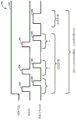
Referring briefly to fig. 2, fig. 2(a) shows a structure 202 that includes a substrate 204 having gaps 206, 208, and 210 formed therein, and a carbon layer 212 covering a surface 214 of the substrate 204. Fig. 2(b) shows a structure 216 comprising a substrate 218 having gaps 220, 222, and 224 formed therein, and a carbon layer 226 covering a surface 228 of the substrate 218. The deposition conditions for structures 202, 216 are the same, except that the precursor used to form structure 202 is 1,3,5, trimethylcyclohexane and the precursor used to form structure 216 is 1,3,5, trimethylbenzene, indicating that the use of a precursor having at least one carbon (e.g., carbon-carbon) double bond may be beneficial for filling recesses while reducing any void formation.
The flow rate of the carbon precursor from the carbon precursor source to the reaction chamber may vary depending on other process conditions. For example, the flow rate can be about 100sccm to about 3,000 sccm. Similarly, the duration of each step of providing the carbon precursor to the reaction chamber may vary depending on various considerations. For example, the duration may be in a range of about 1.0 second to about 35.0 seconds.
During the step of forming a plasma within the reaction chamber to form an initial viscous carbon material on the surface of the substrate, the precursor is converted to the initial viscous material using excited species. The initial viscous carbon material may be changed to a carbon material, for example, by further reaction with excited species. The carbon material may be solid or substantially solid.
During the step of stopping the flow of the carbon precursor to the reaction chamber, the flow of the carbon precursor to the reaction chamber is stopped. In some cases, the flow of precursor may be reduced and not completely shut down for various steps.
During the step of stopping the plasma, the plasma may be extinguished. The stopping step may include reducing power used to generate the plasma.
The step of treating the carbon material with an active species to form a treated carbon material comprises exposing the carbon material to the active species-for example, to an active species formed using a plasma. The treating step may include forming the species from an inert gas, such as an inert gas provided during the step of providing the inert gas to the reaction chamber. The power used to form the plasma may be in the range of about 50W to about 800W. The frequency of the power may be in the range of about 2.0MHz to about 27.12 MHz.
According to exemplary aspects of the present disclosure, the active species are formed by using plasma (e.g., radio frequency and/or microwave plasma). Direct plasma and/or remote plasma may be used to form the active species. In some cases, the inert gas may flow continuously to the reaction chamber and the active species may be formed periodically by cycling the power used to form the plasma. The temperature within the reaction chamber may be less than or equal to 100 ℃ during the step of processing the carbon material. The pressure within the reaction chamber may be about 200Pa to about 1,250Pa during formation of the species to be treated. The speciation for a process step may be formed in the same reaction chamber as for one or more other steps, or may be a separate reaction chamber, such as another reaction chamber of the same cluster tool.
The steps of the various methods described herein may overlap and need not be performed in the order described above. Further, in some cases, various steps or portions thereof may be repeated one or more times before the method proceeds to the next step.
Fig. 1 and 3-7 illustrate examples of pulse timing sequences for methods according to exemplary embodiments of the present disclosure. The figure schematically shows inert gas, carbon precursor and plasma power pulses, wherein gas and/or plasma power is provided to the reactor system over a pulse period. The width of a pulse does not necessarily indicate the amount of time associated with each pulse; the illustrated pulses may illustrate the relative start times of the various pulses. Similarly, height does not necessarily indicate a particular amplitude or value, but may display relatively high and low values. These examples are illustrative only and are not intended to limit the scope of the disclosure or claims.
Fig. 1 illustrates a method 100. The method 100 includes a plurality of carbon material deposition cycles i, ii.. N and a plurality of deposition and treatment cycles 1,2.. N. According to examples of these embodiments, N and N may be in the range of about 1 to about 50.
The method 100 may include continuously supplying an inert gas to the reaction chamber during one or more carbon material deposition cycles i, ii.. N and/or one or more deposition and treatment cycles 12.. N. In the example shown, the inert gas is provided to the reaction chamber over a pulse period 102 that begins before the first (i) deposition cycle and ends after the last (N) deposition and processing cycle. The pulse period may be simply referred to as a pulse.
After the pulse period 102 is initiated, a carbon precursor is provided to the reaction chamber over a pulse period 104. The pulse period 104 may be in a range of, for example, about 1.0 second to about 35.0 seconds. The time of each pulse period 104 may be the same or different.
After the carbon precursor has begun flowing into the reaction chamber, power to form a plasma is provided over the pulse period 106. Thus, in the example shown, both the inert gas and the carbon precursor are provided to the reaction chamber when the plasma is ignited/formed. Pulse period 106 may range, for example, from about 1.0 second to about 30.0 seconds. The time of each pulse period 106 may be the same or different.
As shown in this example, pulse period 104 and pulse period 106 can stop at about or substantially the same time (e.g., within 10, 5, 2, 1, or 0.5% of each other). Once the flow of carbon precursor to the reaction chamber and the plasma power have been stopped, the reaction chamber may be purged over a purge period or pulse period 108. Pulse period 108 may range, for example, from about 5.0 seconds to about 30.0 seconds. The time of each pulse period 108 may be the same or different.
The power during step 106 (e.g., applied to the electrode) may be in the range of about 100W to about 800W. The frequency of the power may be in the range of about 2.0MHz to about 27.12 MHz.
After pulse period 108, the plasma power may be increased to a desired level for treating the carbon material with the active species over pulse period 110. The power level and pressure within the reaction chamber may be as described above. Pulse period 110 may range, for example, from about 1.0 second to about 30.0 seconds. The time of each pulse period 110 may be the same or different.
Following the step of treating the carbon material with the active species over the pulse period 110, the reaction chamber may be purged over the pulse period 112. Pulse period 112 may range, for example, from about 10.0 seconds to about 70.0 seconds. The time of each pulse period 112 may be the same or different.
Fig. 3 shows another method 300. Similar to the method 100, the method 300 includes a plurality of carbon material deposition cycles i, ii.. N and one or more deposition and one treatment steps or cycles 1.. N. According to examples of these embodiments, N may be in the range of about 1 to about 50, and N may be in the range of about 1 to about 50.
The method 300 may include continuously supplying an inert gas to the reaction chamber during one or more carbon material deposition cycles i, ii.. N and/or one or more deposition and one processing steps 1,2,3,4 … N. In the example shown, the inert gas is provided to the reaction chamber over a pulse period 302 that begins before the first (i) deposition cycle and ends after the last (N) deposition and processing cycle.
After the initiation of pulse period 302, a carbon precursor is provided to the reaction chamber on pulse 304. Pulse period 304 may range, for example, from about 1.0 second to about 5.0 seconds.
After the carbon precursor has begun flowing to the reaction chamber, power to form a plasma is provided over the pulse period 306. In the example shown, the flow of the carbon precursor is stopped before the plasma is ignited/formed. Although this method may be suitable for some applications, the method 300 may produce undesirably high particles, e.g., much larger than 50 detectable particles above 50nm in size, on a 300mm wafer on the surface of a treated carbon layer having a layer thickness of 100nm or greater.
In contrast, fig. 1 and 4-7 illustrate a method of relatively low deposition (e.g., less than 50, 40, 30, 10, or 5 particles with a detectable size of greater than 50 nm) of carbon material on a 300mm wafer on the surface of a treated carbon layer having a layer thickness of 100nm or greater. One technique to reduce the number of particles on the surface during the method of forming a structure as described herein includes maintaining power for plasma formation while the carbon precursor flow is stopped.
Fig. 4 illustrates a method 400 according to an example of the present disclosure. The method 400 includes a plurality of carbon material deposition cycles i, ii.. N and one or more deposition and one treatment steps 1.. N. According to examples of these embodiments, N may be in the range of about 1 to about 50, and N may be in the range of about 1 to about 50.
The method 400 may include continuously supplying an inert gas to the reaction chamber during one or more carbon material deposition cycles i, ii.. N and/or one or more deposition and one treatment cycles 1 … N. In the example shown, the inert gas is provided to the reaction chamber over a pulse period 402 that begins before the first (i) deposition cycle and ends after the last (N) deposition and processing cycle.
After initiation of pulse 402, power to form a plasma is provided over pulse period 406. An inert gas may be used to ignite the plasma. The plasma may be continuous for the duration of the pulse period 406. Pulse period 406 may range, for example, from about 3.0 seconds to about 3,600.0 seconds. The power during pulse period 406 (e.g., applied to the electrodes) may be in the range of about 100W to about 800W. The frequency of the power may be in the range of about 2.0MHz to about 27.12 MHz.
Once the plasma is formed, a carbon precursor pulse period 404 can begin. In the example shown, both an inert gas and a carbon precursor are provided to the reaction chamber during pulse period 404. At the end of pulse period 404, the inert gas pulse and the plasma power pulse continue. This is believed to help reduce particles on the substrate surface or layers on the substrate that would otherwise form on the surface during the carbon material deposition cycle, such as may form during method 300. The duration of pulse period 404 may be in a range of, for example, about 1.0 second to about 30.0 seconds. Pulse period 404 may be performed n times before processing pulse 410.
The reaction chamber may be purged over a pulse period 408. During this time, power for plasma formation may be continuously supplied to the reactor system. Similarly, after n carbon material deposition cycles, the reaction chamber may be purged over a pulse period 412. Also, after the process step 410, i.e., after the deposition and process cycle N, the reaction chamber may be purged over a pulse period 414. The next deposition and treatment cycle can then begin if desired. As mentioned above, the time of one or more pulses may be the same or different.
Fig. 5 illustrates another method 500 according to an example of the present disclosure. Method 500 is similar to method 400 except that the i, ii.. n plasma power is pulsed for each carbon material deposition cycle.
The method 500 may include continuously supplying an inert gas to the reaction chamber during one or more carbon material deposition cycles i, ii.. N and/or one or more deposition and one treatment cycles 1,2,3,4 … N. In the example shown, the inert gas is provided to the reaction chamber over a pulse period 502 that begins before the first deposition cycle and ends after the last (N) deposition and processing cycle.
After initiation of pulse period 502, power to form a plasma is provided over pulse period 506. An inert gas may be used to ignite the plasma. In the illustrated example, the pulse period 506 continues after the flow of the carbon precursor is stopped (pulse period 504). The pulse period 506 may be in a range of, for example, about 1.0 second to about 20.0 seconds. The power during pulse period 506 (e.g., applied to the electrodes) may be in the range of about 100W to about 800W. The frequency of the power may be in the range of about 2.0MHz to about 27.12 MHz.
Once the plasma is formed, a carbon precursor pulse period 504 can begin. In the example shown, both an inert gas and a carbon precursor are provided to the reaction chamber during the pulse period 504. At the end of pulse period 504, the inert gas pulse and the plasma power pulse continue. This is again believed to help reduce particles that would otherwise form on the surface of the substrate during the carbon material deposition cycle. The duration of pulse period 504 may be in a range of, for example, about 1.0 second to about 30.0 seconds. Pulse period 504 and pulse period 506 may be performed n times before processing pulse period 510.
During the process step, the inert gas pulse period 502 continues and the power to form the plasma is again increased to the desired level over the pulse period 510. The power during pulse period 510 (e.g., applied to the electrodes) may be in the range of about 100W to about 800W. The frequency of the power may be in the range of about 2.0MHz to about 27.12 MHz. The duration of pulse period 510 may be in a range of, for example, about 1.0 second to about 30.0 seconds.
Between pulse periods 504, the reaction chamber may be purged on pulse period 508. During at least a portion of this time, power applied to the plasma formation may be supplied to the reactor system. Similarly, after n carbon material deposition cycles, the reaction chamber may be purged over a pulse period 512. During at least a portion of the pulse period 512, the reactor system may be supplied with power applied for plasma formation. After the process step 510, i.e., after the deposition and process cycle N, the reaction chamber may be purged for a pulse period 514. The next deposition and treatment cycle can then begin if desired. As noted above, the time of one or more pulses may be the same or different for each cycle.
Fig. 6 shows a method 600 having one carbon material deposition cycle 601 for each deposition and processing cycle 605, followed by a processing step 603.
Similar to methods 400, 500, method 600 may include continuously supplying an inert gas to the reaction chamber during a carbon material deposition cycle 601 and a deposition and processing cycle 605. One deposition step and one treatment N times may be performed. N may range from about 1 to about 50. In the example shown, the inert gas is provided to the reaction chamber over a pulse period 602 that begins before the deposition cycle 601 and ends after the deposition and processing cycle 605.
After initiation of pulse period 602, power to form a plasma is provided over pulse period 606. An inert gas may be used to ignite the plasma. In the illustrated example, the pulse period 606 continues after the flow of the carbon precursor is stopped (pulse period 604). Pulse period 606 may be in a range of, for example, about 3.0 seconds to about 1,000.0 seconds. The power during pulse period 604 (e.g., applied to the electrodes) may be in the range of about 100W to about 800W. The frequency of the power may be in the range of about 2.0MHz to about 27.12 MHz.
Once the plasma is formed, a carbon precursor pulse period 604 can begin. In the example shown, both an inert gas and a carbon precursor are provided to the reaction chamber during pulse period 604. At the end of pulse period 604, the inert gas pulse and the plasma power pulse continue. This is again believed to help reduce particles that would otherwise form on the surface of the substrate during the carbon material deposition cycle. The duration of pulse period 604 may be in a range of, for example, about 1.0 second to about 30.0 seconds.
During process step 603, the inert gas pulse period 602 continues and the power to form the plasma is again increased to the desired level. The power during pulse period 610 (e.g., applied to the electrodes) may be in the range of about 100W to about 800W. The frequency of the power may be in the range of about 2.0MHz to about 27.12 MHz. The duration of pulse period 610 may be in a range of, for example, about 1.0 second to about 30.0 seconds.
After pulse period 604, the reaction chamber may be purged for pulse period 608. During at least a portion of this time, power applied for plasma formation may be supplied to the reactor system such that power is supplied while stopping the carbon precursor flow. Similarly, after the carbon material deposition and treatment cycle 605, the reaction chamber may be purged over a pulse period 612. During at least a portion of the pulse period 612, the reactor system may be supplied with power applied for plasma formation. As described above, the time of each pulse for each cycle may be the same or different.
Fig. 7 illustrates a method 700 in accordance with still further examples of the present disclosure. Method 700 may be similar to method 100, with method 700 showing additional firing and transition steps. Any of the methods described herein may include an ignition and/or transition step.
Similar to the method 100, the method 700 may include continuously supplying an inert gas to the reaction chamber during one carbon material deposition cycle 701 and/or one deposition and processing cycle 709. One deposition step and one treatment were performed N times. N may range from about 1 to about 50. In the example shown, the inert gas is provided to the reaction chamber over a pulse period 702 that begins before the deposition cycle 701 and ends after the deposition and processing cycle 709.
After initiation of pulse period 702, power to form a plasma is provided over pulse period 706. An inert gas may be used to ignite the plasma. In the illustrated example, the pulse period 706 stops at the same time as the carbon precursor stops flowing (pulse period 704) or after the carbon precursor stops flowing. The pulse period 706 may be in a range of, for example, about 3.0 seconds to about 40.0 seconds. The power during pulse period 706 (e.g., applied to the electrodes) may be in the range of about 100W to about 800W. The frequency of the power may be in the range of about 2.0MHz to about 27.12 MHz.
Upon providing power to the plasma, an ignition cycle 705 begins. The ignition cycle 705 may continue until the plasma stabilizes and/or until the carbon precursor pulse cycle 704 is initiated. The duration of the ignition period 705 may be in the range of, for example, about 2.0 seconds to about 10.0 seconds.
Once the plasma is formed, a carbon precursor pulse period 704 can begin. In the example shown, both an inert gas and a carbon precursor are provided to the reaction chamber during the pulse period 704. At the end of pulse period 704 and/or pulse period 706, the inert gas continues in transition period 707. The duration of pulse period 704 may be in a range of, for example, about 1.0 second to about 30.0 seconds. The duration of the ignition period 705 may be in the range of, for example, about 2.0 seconds to about 10.0 seconds.
At the end of the transition period 707, the power of the plasma is increased to again form the plasma. During process step 703 (pulse period 710), the inert gas pulse period 702 continues and the power to form the plasma is maintained at a desired level. The power during pulse period 710 (e.g., applied to the electrodes) may be in the range of about 100W to about 800W. The frequency of the power may be in the range of about 2.0MHz to about 27.12 MHz. The duration of pulse period 710 may be in a range of, for example, about 1.0 second to about 30.0 seconds.
After the pulse period 704, the reaction chamber may be purged over a transition period 707. During at least a portion of this time, power applied for plasma formation may be supplied to the reactor system such that power is supplied while stopping the carbon precursor flow. Similarly, after the carbon material deposition cycle and the process cycle 709, the reaction chamber may be purged over a pulse period 712. During at least a portion of pulse period 712, power for plasma formation may be turned off. The duration of each pulse of the different cycles may be the same or may be different.
FIG. 8 illustrates a reactor system 800 according to an exemplary embodiment of the present disclosure. Reactor system 800 may be used to perform one or more steps or sub-steps as described herein, and/or to form one or more structures or portions thereof as described herein.
The reactor system 800 comprises a pair of electrically conductive plate electrodes 4, 2 parallel and facing each other in the interior 11 (reaction zone) of the reaction chamber 3. Plasma can be ignited within reaction chamber 3 by applying HRF power (e.g., 13.56MHz or 27MHz) from power supply 25 to one electrode (e.g., electrode 4) and electrically grounding the other electrode (e.g., electrode 2). A temperature regulator is provided in the lower stage 2 (lower electrode), and the temperature of the substrate 1 placed on the lower stage can be maintained at a desired temperature. The electrode 4 may act as a gas distribution device, such as a shower plate. The reaction gas, the dilution gas (if present), the precursor gas, etc. may be introduced into the reaction chamber 3 through the shower plate 4 using one or more of a gas line 20, a gas line 21, and a gas line 22, respectively. Although three gas lines are shown, reactor system 800 can include any suitable number of gas lines.
In the reaction chamber 3, an annular duct 13 with an exhaust line 7 is provided, through which the gases in the interior 11 of the reaction chamber 3 are exhausted. In addition, the transfer chamber 5 disposed below the reaction chamber 3 is provided with a seal gas line 24 to introduce a seal gas into the interior 11 of the reaction chamber 3 through the interior 16 (transfer region) of the transfer chamber 5, wherein a separation plate 14 for separating the reaction region and the transfer region is provided (this figure omits a gate valve through which a wafer is transferred into or from the transfer chamber 5). The transfer chamber is also provided with an exhaust line 6. In some embodiments, the deposition and processing steps are performed in the same reaction space such that two or more (e.g., all) steps can be performed continuously without exposing the substrate to air or other oxygen-containing atmosphere.
In some embodiments, the continuous flow of inert or carrier gas to the reaction chamber 3 may be achieved using a flow-through system (FPS), wherein the carrier gas line has a bypass line with a precursor reservoir (bottle), and the main and bypass lines are switched, wherein the bypass line is closed when the carrier gas is intended to be fed only to the reaction chamber, and the main line is closed when both the carrier gas and the precursor gas are intended to be fed to the reaction chamber, and the carrier gas flows through the bypass line and out of the bottle together with the precursor gas. In this way, the carrier gas can flow continuously into the reaction chamber and can carry the precursor gas in pulses by switching between the main and bypass lines without substantially fluctuating the pressure of the reaction chamber.
Those skilled in the art will appreciate that the apparatus includes one or more controllers 26 programmed or otherwise configured to enable one or more of the method steps described elsewhere herein. As will be appreciated by those skilled in the art, the controller(s) are in communication with the gas flow controllers or valves of the various power supplies, heating systems, pumps, robotic devices, and reactors.
In some embodiments, a dual chamber reactor (two sections or compartments for processing wafers disposed closely to each other) may be used in which the reactant and inert gases may be supplied through shared lines and the precursor gases through unshared lines.
The example embodiments of the present disclosure described above do not limit the scope of the present invention, as these embodiments are merely examples of embodiments of the present invention. Any equivalent embodiments are intended to be included within the scope of the present invention. Indeed, various modifications of the disclosure, in addition to those shown and described herein, as alternative suitable combinations of the described elements, will become apparent to those skilled in the art from the description. Such modifications and embodiments are also intended to fall within the scope of the appended claims.
Claims (27)
1. A method of forming a structure, the method comprising the steps of:
providing a substrate within a reaction chamber, the substrate comprising one or more recesses;
providing an inert gas to the reaction chamber for plasma ignition;
providing a carbon precursor to the reaction chamber;
forming a plasma within the reaction chamber to form an initial viscous carbon material on a surface of the substrate, wherein the initial viscous carbon material becomes a carbon material;
stopping the flow of the carbon precursor to the reaction chamber;
stopping the plasma; and
treating the carbon material with an active species to form a treated carbon material.
2. The method of claim 1, wherein the following steps are performed N times to fill the one or more recesses:
providing a carbon precursor to the reaction chamber;
forming a plasma within the reaction chamber to form an initial viscous carbon material on a surface of the substrate;
stopping the flow of the carbon precursor;
stopping the plasma; and
treating the carbon material with an active species.
3. The method of claim 2, wherein N is in the range of about 1 to about 50.
4. The method of any of claims 1-3, wherein treating comprises igniting a plasma within the reaction chamber using the inert gas.
5. The method of any one of claims 1-4, wherein during a carbon material deposition cycle, the step of providing a carbon precursor to the reaction chamber occurs before and continues during the step of forming a plasma within the reaction chamber.
6. The method of any one of claims 1-5, wherein the steps of stopping the flow of the carbon precursor and stopping the plasma occur substantially simultaneously during a carbon material deposition cycle.
7. The method of any one of claims 1-5, wherein during a carbon material deposition cycle, the step of stopping the flow of the carbon precursor occurs before the step of stopping the plasma.
8. The method of any of claims 1-5, wherein the RF power provided to form the plasma is reduced after stopping the flow of the carbon precursor.
9. The method of any one of claims 1-8, wherein the RF power to form the plasma is increased to perform the step of treating the carbon material with the active species.
10. The method of any one of claims 1-9, wherein both the inert gas and the carbon precursor flow to the reaction chamber during the step of forming a plasma within the reaction chamber.
11. The method of any one of claims 1-10, wherein the inert gas is continuously flowed to the reaction chamber during the steps of providing a carbon precursor to the reaction chamber and forming a plasma within the reaction chamber.
12. The method of claim 1, wherein the deposition and treatment cycle comprises:
performing a carbon material deposition cycle one or more times; and then
Treating the carbon material with an active species,
wherein the deposition and treatment cycle is performed a plurality of times for N depositions and one treatment step, an
Wherein the inert gas is continuously flowed to the reaction chamber during the N depositions and one process step.
13. The method of claim 1, wherein the steps of forming a plasma within the reaction chamber to form an initial viscous carbon material on the surface of the substrate and stopping the plasma are repeated a plurality of times prior to the step of treating the carbon material with active species.
14. The method of any one of claims 1-13, wherein during a carbon material deposition cycle, a plasma is continuously formed within the reaction chamber during the steps of providing a carbon precursor to the reaction chamber and stopping the flow of the carbon precursor.
15. The method of claim 1, wherein a plasma is continuously formed within the reaction chamber during the steps of providing a carbon precursor to the reaction chamber, stopping the flow of the carbon precursor, and treating the carbon material with an active species.
16. The method of claim 1, wherein a plasma is continuously formed within the reaction chamber while repeating one or more carbon material deposition cycles.
17. The method of claim 1, wherein plasma is continuously formed within the reaction chamber during at least one carbon material deposition cycle and at least one processing step.
18. The method of any one of claims 1-17, wherein the step of forming a plasma within the reaction chamber to form the initial viscous carbon material has a duration of between about 1.0 seconds and about 30.0 seconds during a carbon material deposition cycle.
19. The method of any one of claims 1-18, wherein the step of treating the carbon material with the active species is for a duration of between about 1.0 seconds and about 30.0 seconds during a deposition and treatment cycle.
20. The method of any one of claims 1-19, wherein the inert gas comprises argon, helium, nitrogen, or any mixture thereof.
21. The method of any one of claims 1-20, wherein the carbon precursor has a formula represented by CxHyNzWhere x is a natural number of 2 or more, y is a natural number, and z is 0 or a natural number.
22. The method of any one of claims 1-21, wherein the carbon precursor comprises a cyclic structure having at least one double bond.
23. The method of any one of claims 1-22, wherein the temperature within the reaction chamber is less than or equal to 100 ℃ during the following steps:
providing the carbon precursor to the reaction chamber;
forming a plasma within the reaction chamber to form the initial viscous carbon material on a surface of the substrate;
stopping the flow of the carbon precursor;
stopping the plasma; and
treating the carbon material with an active species.
24. A film structure formed according to the method of any one of claims 1-23.
25. The film structure of claim 24, wherein the treated carbon layer comprises 45 atomic% or more carbon.
26. The film structure of claim 25, wherein the structure comprises less than 50 particles of detectable size greater than 50nm on a 300mm wafer on the surface of a treated carbon layer having a layer thickness of 100nm or greater.
27. A system for performing the steps of any of claims 1-23 and/or for forming a structure according to any of claims 24-26.
Applications Claiming Priority (2)
| Application Number | Priority Date | Filing Date | Title |
|---|---|---|---|
| US202062970483P | 2020-02-05 | 2020-02-05 | |
| US62/970,483 | 2020-02-05 |
Publications (1)
| Publication Number | Publication Date |
|---|---|
| CN113215550A true CN113215550A (en) | 2021-08-06 |
Family
ID=77061750
Family Applications (1)
| Application Number | Title | Priority Date | Filing Date |
|---|---|---|---|
| CN202110135743.XA Pending CN113215550A (en) | 2020-02-05 | 2021-02-01 | Method of forming a structure, formed structure and system for forming the structure |
Country Status (5)
| Country | Link |
|---|---|
| US (1) | US20210238742A1 (en) |
| JP (1) | JP2021123800A (en) |
| KR (1) | KR20210100535A (en) |
| CN (1) | CN113215550A (en) |
| TW (1) | TW202134465A (en) |
Families Citing this family (160)
| Publication number | Priority date | Publication date | Assignee | Title |
|---|---|---|---|---|
| US20130023129A1 (en) | 2011-07-20 | 2013-01-24 | Asm America, Inc. | Pressure transmitter for a semiconductor processing environment |
| US20160376700A1 (en) | 2013-02-01 | 2016-12-29 | Asm Ip Holding B.V. | System for treatment of deposition reactor |
| US10941490B2 (en) | 2014-10-07 | 2021-03-09 | Asm Ip Holding B.V. | Multiple temperature range susceptor, assembly, reactor and system including the susceptor, and methods of using the same |
| US10276355B2 (en) | 2015-03-12 | 2019-04-30 | Asm Ip Holding B.V. | Multi-zone reactor, system including the reactor, and method of using the same |
| US11139308B2 (en) | 2015-12-29 | 2021-10-05 | Asm Ip Holding B.V. | Atomic layer deposition of III-V compounds to form V-NAND devices |
| US10529554B2 (en) | 2016-02-19 | 2020-01-07 | Asm Ip Holding B.V. | Method for forming silicon nitride film selectively on sidewalls or flat surfaces of trenches |
| US11453943B2 (en) | 2016-05-25 | 2022-09-27 | Asm Ip Holding B.V. | Method for forming carbon-containing silicon/metal oxide or nitride film by ALD using silicon precursor and hydrocarbon precursor |
| US9859151B1 (en) | 2016-07-08 | 2018-01-02 | Asm Ip Holding B.V. | Selective film deposition method to form air gaps |
| US10612137B2 (en) | 2016-07-08 | 2020-04-07 | Asm Ip Holdings B.V. | Organic reactants for atomic layer deposition |
| US9887082B1 (en) | 2016-07-28 | 2018-02-06 | Asm Ip Holding B.V. | Method and apparatus for filling a gap |
| US9812320B1 (en) | 2016-07-28 | 2017-11-07 | Asm Ip Holding B.V. | Method and apparatus for filling a gap |
| US11532757B2 (en) | 2016-10-27 | 2022-12-20 | Asm Ip Holding B.V. | Deposition of charge trapping layers |
| US10714350B2 (en) | 2016-11-01 | 2020-07-14 | ASM IP Holdings, B.V. | Methods for forming a transition metal niobium nitride film on a substrate by atomic layer deposition and related semiconductor device structures |
| KR102546317B1 (en) | 2016-11-15 | 2023-06-21 | 에이에스엠 아이피 홀딩 비.브이. | Gas supply unit and substrate processing apparatus including the same |
| US11447861B2 (en) | 2016-12-15 | 2022-09-20 | Asm Ip Holding B.V. | Sequential infiltration synthesis apparatus and a method of forming a patterned structure |
| US11581186B2 (en) | 2016-12-15 | 2023-02-14 | Asm Ip Holding B.V. | Sequential infiltration synthesis apparatus |
| US11390950B2 (en) | 2017-01-10 | 2022-07-19 | Asm Ip Holding B.V. | Reactor system and method to reduce residue buildup during a film deposition process |
| US10468261B2 (en) | 2017-02-15 | 2019-11-05 | Asm Ip Holding B.V. | Methods for forming a metallic film on a substrate by cyclical deposition and related semiconductor device structures |
| US10770286B2 (en) | 2017-05-08 | 2020-09-08 | Asm Ip Holdings B.V. | Methods for selectively forming a silicon nitride film on a substrate and related semiconductor device structures |
| US11306395B2 (en) | 2017-06-28 | 2022-04-19 | Asm Ip Holding B.V. | Methods for depositing a transition metal nitride film on a substrate by atomic layer deposition and related deposition apparatus |
| KR20190009245A (en) | 2017-07-18 | 2019-01-28 | 에이에스엠 아이피 홀딩 비.브이. | Methods for forming a semiconductor device structure and related semiconductor device structures |
| US10590535B2 (en) | 2017-07-26 | 2020-03-17 | Asm Ip Holdings B.V. | Chemical treatment, deposition and/or infiltration apparatus and method for using the same |
| US10692741B2 (en) | 2017-08-08 | 2020-06-23 | Asm Ip Holdings B.V. | Radiation shield |
| US10770336B2 (en) | 2017-08-08 | 2020-09-08 | Asm Ip Holding B.V. | Substrate lift mechanism and reactor including same |
| US11769682B2 (en) | 2017-08-09 | 2023-09-26 | Asm Ip Holding B.V. | Storage apparatus for storing cassettes for substrates and processing apparatus equipped therewith |
| US11830730B2 (en) | 2017-08-29 | 2023-11-28 | Asm Ip Holding B.V. | Layer forming method and apparatus |
| US11295980B2 (en) | 2017-08-30 | 2022-04-05 | Asm Ip Holding B.V. | Methods for depositing a molybdenum metal film over a dielectric surface of a substrate by a cyclical deposition process and related semiconductor device structures |
| US10658205B2 (en) | 2017-09-28 | 2020-05-19 | Asm Ip Holdings B.V. | Chemical dispensing apparatus and methods for dispensing a chemical to a reaction chamber |
| WO2019103610A1 (en) | 2017-11-27 | 2019-05-31 | Asm Ip Holding B.V. | Apparatus including a clean mini environment |
| CN111316417B (en) | 2017-11-27 | 2023-12-22 | 阿斯莫Ip控股公司 | Storage device for storing wafer cassettes for use with batch ovens |
| US10872771B2 (en) | 2018-01-16 | 2020-12-22 | Asm Ip Holding B. V. | Method for depositing a material film on a substrate within a reaction chamber by a cyclical deposition process and related device structures |
| TW202325889A (en) | 2018-01-19 | 2023-07-01 | 荷蘭商Asm 智慧財產控股公司 | Deposition method |
| WO2019142055A2 (en) | 2018-01-19 | 2019-07-25 | Asm Ip Holding B.V. | Method for depositing a gap-fill layer by plasma-assisted deposition |
| US11081345B2 (en) | 2018-02-06 | 2021-08-03 | Asm Ip Holding B.V. | Method of post-deposition treatment for silicon oxide film |
| US10896820B2 (en) | 2018-02-14 | 2021-01-19 | Asm Ip Holding B.V. | Method for depositing a ruthenium-containing film on a substrate by a cyclical deposition process |
| EP3737779A1 (en) | 2018-02-14 | 2020-11-18 | ASM IP Holding B.V. | A method for depositing a ruthenium-containing film on a substrate by a cyclical deposition process |
| KR102636427B1 (en) | 2018-02-20 | 2024-02-13 | 에이에스엠 아이피 홀딩 비.브이. | Substrate processing method and apparatus |
| US10975470B2 (en) | 2018-02-23 | 2021-04-13 | Asm Ip Holding B.V. | Apparatus for detecting or monitoring for a chemical precursor in a high temperature environment |
| US11473195B2 (en) | 2018-03-01 | 2022-10-18 | Asm Ip Holding B.V. | Semiconductor processing apparatus and a method for processing a substrate |
| KR102646467B1 (en) | 2018-03-27 | 2024-03-11 | 에이에스엠 아이피 홀딩 비.브이. | Method of forming an electrode on a substrate and a semiconductor device structure including an electrode |
| KR102596988B1 (en) | 2018-05-28 | 2023-10-31 | 에이에스엠 아이피 홀딩 비.브이. | Method of processing a substrate and a device manufactured by the same |
| US11718913B2 (en) | 2018-06-04 | 2023-08-08 | Asm Ip Holding B.V. | Gas distribution system and reactor system including same |
| KR102568797B1 (en) | 2018-06-21 | 2023-08-21 | 에이에스엠 아이피 홀딩 비.브이. | Substrate processing system |
| US10797133B2 (en) | 2018-06-21 | 2020-10-06 | Asm Ip Holding B.V. | Method for depositing a phosphorus doped silicon arsenide film and related semiconductor device structures |
| JP2021529254A (en) | 2018-06-27 | 2021-10-28 | エーエスエム・アイピー・ホールディング・ベー・フェー | Periodic deposition methods for forming metal-containing materials and films and structures containing metal-containing materials |
| US11499222B2 (en) | 2018-06-27 | 2022-11-15 | Asm Ip Holding B.V. | Cyclic deposition methods for forming metal-containing material and films and structures including the metal-containing material |
| US10388513B1 (en) * | 2018-07-03 | 2019-08-20 | Asm Ip Holding B.V. | Method for depositing silicon-free carbon-containing film as gap-fill layer by pulse plasma-assisted deposition |
| US10755922B2 (en) | 2018-07-03 | 2020-08-25 | Asm Ip Holding B.V. | Method for depositing silicon-free carbon-containing film as gap-fill layer by pulse plasma-assisted deposition |
| US11430674B2 (en) | 2018-08-22 | 2022-08-30 | Asm Ip Holding B.V. | Sensor array, apparatus for dispensing a vapor phase reactant to a reaction chamber and related methods |
| US11024523B2 (en) | 2018-09-11 | 2021-06-01 | Asm Ip Holding B.V. | Substrate processing apparatus and method |
| KR20200030162A (en) | 2018-09-11 | 2020-03-20 | 에이에스엠 아이피 홀딩 비.브이. | Method for deposition of a thin film |
| CN110970344A (en) | 2018-10-01 | 2020-04-07 | Asm Ip控股有限公司 | Substrate holding apparatus, system including the same, and method of using the same |
| KR102592699B1 (en) | 2018-10-08 | 2023-10-23 | 에이에스엠 아이피 홀딩 비.브이. | Substrate support unit and apparatuses for depositing thin film and processing the substrate including the same |
| KR102546322B1 (en) | 2018-10-19 | 2023-06-21 | 에이에스엠 아이피 홀딩 비.브이. | Substrate processing apparatus and substrate processing method |
| US11087997B2 (en) | 2018-10-31 | 2021-08-10 | Asm Ip Holding B.V. | Substrate processing apparatus for processing substrates |
| KR20200051105A (en) | 2018-11-02 | 2020-05-13 | 에이에스엠 아이피 홀딩 비.브이. | Substrate support unit and substrate processing apparatus including the same |
| US11572620B2 (en) | 2018-11-06 | 2023-02-07 | Asm Ip Holding B.V. | Methods for selectively depositing an amorphous silicon film on a substrate |
| US10818758B2 (en) | 2018-11-16 | 2020-10-27 | Asm Ip Holding B.V. | Methods for forming a metal silicate film on a substrate in a reaction chamber and related semiconductor device structures |
| KR102636428B1 (en) | 2018-12-04 | 2024-02-13 | 에이에스엠 아이피 홀딩 비.브이. | A method for cleaning a substrate processing apparatus |
| US11158513B2 (en) | 2018-12-13 | 2021-10-26 | Asm Ip Holding B.V. | Methods for forming a rhenium-containing film on a substrate by a cyclical deposition process and related semiconductor device structures |
| JP2020096183A (en) | 2018-12-14 | 2020-06-18 | エーエスエム・アイピー・ホールディング・ベー・フェー | Method of forming device structure using selective deposition of gallium nitride, and system for the same |
| TWI819180B (en) | 2019-01-17 | 2023-10-21 | 荷蘭商Asm 智慧財產控股公司 | Methods of forming a transition metal containing film on a substrate by a cyclical deposition process |
| JP2020136678A (en) | 2019-02-20 | 2020-08-31 | エーエスエム・アイピー・ホールディング・ベー・フェー | Method for filing concave part formed inside front surface of base material, and device |
| US11482533B2 (en) | 2019-02-20 | 2022-10-25 | Asm Ip Holding B.V. | Apparatus and methods for plug fill deposition in 3-D NAND applications |
| TW202104632A (en) | 2019-02-20 | 2021-02-01 | 荷蘭商Asm Ip私人控股有限公司 | Cyclical deposition method and apparatus for filling a recess formed within a substrate surface |
| TW202100794A (en) | 2019-02-22 | 2021-01-01 | 荷蘭商Asm Ip私人控股有限公司 | Substrate processing apparatus and method for processing substrate |
| KR20200108242A (en) | 2019-03-08 | 2020-09-17 | 에이에스엠 아이피 홀딩 비.브이. | Method for Selective Deposition of Silicon Nitride Layer and Structure Including Selectively-Deposited Silicon Nitride Layer |
| US11742198B2 (en) | 2019-03-08 | 2023-08-29 | Asm Ip Holding B.V. | Structure including SiOCN layer and method of forming same |
| JP2020167398A (en) | 2019-03-28 | 2020-10-08 | エーエスエム・アイピー・ホールディング・ベー・フェー | Door opener and substrate processing apparatus provided therewith |
| KR20200116855A (en) | 2019-04-01 | 2020-10-13 | 에이에스엠 아이피 홀딩 비.브이. | Method of manufacturing semiconductor device |
| US11447864B2 (en) | 2019-04-19 | 2022-09-20 | Asm Ip Holding B.V. | Layer forming method and apparatus |
| KR20200125453A (en) | 2019-04-24 | 2020-11-04 | 에이에스엠 아이피 홀딩 비.브이. | Gas-phase reactor system and method of using same |
| KR20200130121A (en) | 2019-05-07 | 2020-11-18 | 에이에스엠 아이피 홀딩 비.브이. | Chemical source vessel with dip tube |
| KR20200130652A (en) | 2019-05-10 | 2020-11-19 | 에이에스엠 아이피 홀딩 비.브이. | Method of depositing material onto a surface and structure formed according to the method |
| JP2020188255A (en) | 2019-05-16 | 2020-11-19 | エーエスエム アイピー ホールディング ビー.ブイ. | Wafer boat handling device, vertical batch furnace, and method |
| USD975665S1 (en) | 2019-05-17 | 2023-01-17 | Asm Ip Holding B.V. | Susceptor shaft |
| USD947913S1 (en) | 2019-05-17 | 2022-04-05 | Asm Ip Holding B.V. | Susceptor shaft |
| KR20200141002A (en) | 2019-06-06 | 2020-12-17 | 에이에스엠 아이피 홀딩 비.브이. | Method of using a gas-phase reactor system including analyzing exhausted gas |
| KR20200143254A (en) | 2019-06-11 | 2020-12-23 | 에이에스엠 아이피 홀딩 비.브이. | Method of forming an electronic structure using an reforming gas, system for performing the method, and structure formed using the method |
| KR20210005515A (en) | 2019-07-03 | 2021-01-14 | 에이에스엠 아이피 홀딩 비.브이. | Temperature control assembly for substrate processing apparatus and method of using same |
| JP2021015791A (en) | 2019-07-09 | 2021-02-12 | エーエスエム アイピー ホールディング ビー.ブイ. | Plasma device and substrate processing method using coaxial waveguide |
| CN112216646A (en) | 2019-07-10 | 2021-01-12 | Asm Ip私人控股有限公司 | Substrate supporting assembly and substrate processing device comprising same |
| KR20210010307A (en) | 2019-07-16 | 2021-01-27 | 에이에스엠 아이피 홀딩 비.브이. | Substrate processing apparatus |
| KR20210010820A (en) | 2019-07-17 | 2021-01-28 | 에이에스엠 아이피 홀딩 비.브이. | Methods of forming silicon germanium structures |
| KR20210010816A (en) | 2019-07-17 | 2021-01-28 | 에이에스엠 아이피 홀딩 비.브이. | Radical assist ignition plasma system and method |
| US11643724B2 (en) | 2019-07-18 | 2023-05-09 | Asm Ip Holding B.V. | Method of forming structures using a neutral beam |
| CN112309843A (en) | 2019-07-29 | 2021-02-02 | Asm Ip私人控股有限公司 | Selective deposition method for achieving high dopant doping |
| CN112309900A (en) | 2019-07-30 | 2021-02-02 | Asm Ip私人控股有限公司 | Substrate processing apparatus |
| CN112309899A (en) | 2019-07-30 | 2021-02-02 | Asm Ip私人控股有限公司 | Substrate processing apparatus |
| US11587815B2 (en) | 2019-07-31 | 2023-02-21 | Asm Ip Holding B.V. | Vertical batch furnace assembly |
| US11587814B2 (en) | 2019-07-31 | 2023-02-21 | Asm Ip Holding B.V. | Vertical batch furnace assembly |
| US11227782B2 (en) | 2019-07-31 | 2022-01-18 | Asm Ip Holding B.V. | Vertical batch furnace assembly |
| KR20210018759A (en) | 2019-08-05 | 2021-02-18 | 에이에스엠 아이피 홀딩 비.브이. | Liquid level sensor for a chemical source vessel |
| USD965524S1 (en) | 2019-08-19 | 2022-10-04 | Asm Ip Holding B.V. | Susceptor support |
| USD965044S1 (en) | 2019-08-19 | 2022-09-27 | Asm Ip Holding B.V. | Susceptor shaft |
| JP2021031769A (en) | 2019-08-21 | 2021-03-01 | エーエスエム アイピー ホールディング ビー.ブイ. | Production apparatus of mixed gas of film deposition raw material and film deposition apparatus |
| KR20210024423A (en) | 2019-08-22 | 2021-03-05 | 에이에스엠 아이피 홀딩 비.브이. | Method for forming a structure with a hole |
| USD979506S1 (en) | 2019-08-22 | 2023-02-28 | Asm Ip Holding B.V. | Insulator |
| US11286558B2 (en) | 2019-08-23 | 2022-03-29 | Asm Ip Holding B.V. | Methods for depositing a molybdenum nitride film on a surface of a substrate by a cyclical deposition process and related semiconductor device structures including a molybdenum nitride film |
| KR20210029090A (en) | 2019-09-04 | 2021-03-15 | 에이에스엠 아이피 홀딩 비.브이. | Methods for selective deposition using a sacrificial capping layer |
| KR20210029663A (en) | 2019-09-05 | 2021-03-16 | 에이에스엠 아이피 홀딩 비.브이. | Substrate processing apparatus |
| US11562901B2 (en) | 2019-09-25 | 2023-01-24 | Asm Ip Holding B.V. | Substrate processing method |
| CN112593212B (en) | 2019-10-02 | 2023-12-22 | Asm Ip私人控股有限公司 | Method for forming topologically selective silicon oxide film by cyclic plasma enhanced deposition process |
| TW202129060A (en) | 2019-10-08 | 2021-08-01 | 荷蘭商Asm Ip控股公司 | Substrate processing device, and substrate processing method |
| TW202115273A (en) | 2019-10-10 | 2021-04-16 | 荷蘭商Asm Ip私人控股有限公司 | Method of forming a photoresist underlayer and structure including same |
| KR20210045930A (en) | 2019-10-16 | 2021-04-27 | 에이에스엠 아이피 홀딩 비.브이. | Method of Topology-Selective Film Formation of Silicon Oxide |
| US11637014B2 (en) | 2019-10-17 | 2023-04-25 | Asm Ip Holding B.V. | Methods for selective deposition of doped semiconductor material |
| KR20210047808A (en) | 2019-10-21 | 2021-04-30 | 에이에스엠 아이피 홀딩 비.브이. | Apparatus and methods for selectively etching films |
| US11646205B2 (en) | 2019-10-29 | 2023-05-09 | Asm Ip Holding B.V. | Methods of selectively forming n-type doped material on a surface, systems for selectively forming n-type doped material, and structures formed using same |
| KR20210054983A (en) | 2019-11-05 | 2021-05-14 | 에이에스엠 아이피 홀딩 비.브이. | Structures with doped semiconductor layers and methods and systems for forming same |
| US11501968B2 (en) | 2019-11-15 | 2022-11-15 | Asm Ip Holding B.V. | Method for providing a semiconductor device with silicon filled gaps |
| KR20210062561A (en) | 2019-11-20 | 2021-05-31 | 에이에스엠 아이피 홀딩 비.브이. | Method of depositing carbon-containing material on a surface of a substrate, structure formed using the method, and system for forming the structure |
| KR20210065848A (en) | 2019-11-26 | 2021-06-04 | 에이에스엠 아이피 홀딩 비.브이. | Methods for selectivley forming a target film on a substrate comprising a first dielectric surface and a second metallic surface |
| CN112951697A (en) | 2019-11-26 | 2021-06-11 | Asm Ip私人控股有限公司 | Substrate processing apparatus |
| CN112885693A (en) | 2019-11-29 | 2021-06-01 | Asm Ip私人控股有限公司 | Substrate processing apparatus |
| CN112885692A (en) | 2019-11-29 | 2021-06-01 | Asm Ip私人控股有限公司 | Substrate processing apparatus |
| JP2021090042A (en) | 2019-12-02 | 2021-06-10 | エーエスエム アイピー ホールディング ビー.ブイ. | Substrate processing apparatus and substrate processing method |
| KR20210070898A (en) | 2019-12-04 | 2021-06-15 | 에이에스엠 아이피 홀딩 비.브이. | Substrate processing apparatus |
| TW202125596A (en) | 2019-12-17 | 2021-07-01 | 荷蘭商Asm Ip私人控股有限公司 | Method of forming vanadium nitride layer and structure including the vanadium nitride layer |
| US11527403B2 (en) | 2019-12-19 | 2022-12-13 | Asm Ip Holding B.V. | Methods for filling a gap feature on a substrate surface and related semiconductor structures |
| KR20210095050A (en) | 2020-01-20 | 2021-07-30 | 에이에스엠 아이피 홀딩 비.브이. | Method of forming thin film and method of modifying surface of thin film |
| TW202130846A (en) | 2020-02-03 | 2021-08-16 | 荷蘭商Asm Ip私人控股有限公司 | Method of forming structures including a vanadium or indium layer |
| KR20210100010A (en) | 2020-02-04 | 2021-08-13 | 에이에스엠 아이피 홀딩 비.브이. | Method and apparatus for transmittance measurements of large articles |
| US11776846B2 (en) | 2020-02-07 | 2023-10-03 | Asm Ip Holding B.V. | Methods for depositing gap filling fluids and related systems and devices |
| US11781243B2 (en) | 2020-02-17 | 2023-10-10 | Asm Ip Holding B.V. | Method for depositing low temperature phosphorous-doped silicon |
| KR20210116240A (en) | 2020-03-11 | 2021-09-27 | 에이에스엠 아이피 홀딩 비.브이. | Substrate handling device with adjustable joints |
| US11876356B2 (en) | 2020-03-11 | 2024-01-16 | Asm Ip Holding B.V. | Lockout tagout assembly and system and method of using same |
| CN113394086A (en) | 2020-03-12 | 2021-09-14 | Asm Ip私人控股有限公司 | Method for producing a layer structure having a target topological profile |
| KR20210124042A (en) | 2020-04-02 | 2021-10-14 | 에이에스엠 아이피 홀딩 비.브이. | Thin film forming method |
| TW202146689A (en) | 2020-04-03 | 2021-12-16 | 荷蘭商Asm Ip控股公司 | Method for forming barrier layer and method for manufacturing semiconductor device |
| TW202145344A (en) | 2020-04-08 | 2021-12-01 | 荷蘭商Asm Ip私人控股有限公司 | Apparatus and methods for selectively etching silcon oxide films |
| US11821078B2 (en) | 2020-04-15 | 2023-11-21 | Asm Ip Holding B.V. | Method for forming precoat film and method for forming silicon-containing film |
| KR20210132605A (en) | 2020-04-24 | 2021-11-04 | 에이에스엠 아이피 홀딩 비.브이. | Vertical batch furnace assembly comprising a cooling gas supply |
| KR20210132600A (en) | 2020-04-24 | 2021-11-04 | 에이에스엠 아이피 홀딩 비.브이. | Methods and systems for depositing a layer comprising vanadium, nitrogen, and a further element |
| TW202140831A (en) | 2020-04-24 | 2021-11-01 | 荷蘭商Asm Ip私人控股有限公司 | Method of forming vanadium nitride–containing layer and structure comprising the same |
| KR20210134226A (en) | 2020-04-29 | 2021-11-09 | 에이에스엠 아이피 홀딩 비.브이. | Solid source precursor vessel |
| KR20210134869A (en) | 2020-05-01 | 2021-11-11 | 에이에스엠 아이피 홀딩 비.브이. | Fast FOUP swapping with a FOUP handler |
| KR20210141379A (en) | 2020-05-13 | 2021-11-23 | 에이에스엠 아이피 홀딩 비.브이. | Laser alignment fixture for a reactor system |
| KR20210143653A (en) | 2020-05-19 | 2021-11-29 | 에이에스엠 아이피 홀딩 비.브이. | Substrate processing apparatus |
| KR20210145078A (en) | 2020-05-21 | 2021-12-01 | 에이에스엠 아이피 홀딩 비.브이. | Structures including multiple carbon layers and methods of forming and using same |
| TW202201602A (en) | 2020-05-29 | 2022-01-01 | 荷蘭商Asm Ip私人控股有限公司 | Substrate processing device |
| TW202218133A (en) | 2020-06-24 | 2022-05-01 | 荷蘭商Asm Ip私人控股有限公司 | Method for forming a layer provided with silicon |
| TW202217953A (en) | 2020-06-30 | 2022-05-01 | 荷蘭商Asm Ip私人控股有限公司 | Substrate processing method |
| KR20220010438A (en) | 2020-07-17 | 2022-01-25 | 에이에스엠 아이피 홀딩 비.브이. | Structures and methods for use in photolithography |
| TW202204662A (en) | 2020-07-20 | 2022-02-01 | 荷蘭商Asm Ip私人控股有限公司 | Method and system for depositing molybdenum layers |
| KR20220027026A (en) | 2020-08-26 | 2022-03-07 | 에이에스엠 아이피 홀딩 비.브이. | Method and system for forming metal silicon oxide and metal silicon oxynitride |
| USD990534S1 (en) | 2020-09-11 | 2023-06-27 | Asm Ip Holding B.V. | Weighted lift pin |
| USD1012873S1 (en) | 2020-09-24 | 2024-01-30 | Asm Ip Holding B.V. | Electrode for semiconductor processing apparatus |
| TW202229613A (en) | 2020-10-14 | 2022-08-01 | 荷蘭商Asm Ip私人控股有限公司 | Method of depositing material on stepped structure |
| KR20220053482A (en) | 2020-10-22 | 2022-04-29 | 에이에스엠 아이피 홀딩 비.브이. | Method of depositing vanadium metal, structure, device and a deposition assembly |
| TW202223136A (en) | 2020-10-28 | 2022-06-16 | 荷蘭商Asm Ip私人控股有限公司 | Method for forming layer on substrate, and semiconductor processing system |
| KR20220076343A (en) | 2020-11-30 | 2022-06-08 | 에이에스엠 아이피 홀딩 비.브이. | an injector configured for arrangement within a reaction chamber of a substrate processing apparatus |
| US11946137B2 (en) | 2020-12-16 | 2024-04-02 | Asm Ip Holding B.V. | Runout and wobble measurement fixtures |
| TW202231903A (en) | 2020-12-22 | 2022-08-16 | 荷蘭商Asm Ip私人控股有限公司 | Transition metal deposition method, transition metal layer, and deposition assembly for depositing transition metal on substrate |
| TW202233886A (en) * | 2021-02-05 | 2022-09-01 | 荷蘭商Asm Ip私人控股有限公司 | Methods of filling recesses on substrate surface, structures formed using the methods, and systems for forming same |
| USD981973S1 (en) | 2021-05-11 | 2023-03-28 | Asm Ip Holding B.V. | Reactor wall for substrate processing apparatus |
| USD1023959S1 (en) | 2021-05-11 | 2024-04-23 | Asm Ip Holding B.V. | Electrode for substrate processing apparatus |
| USD980814S1 (en) | 2021-05-11 | 2023-03-14 | Asm Ip Holding B.V. | Gas distributor for substrate processing apparatus |
| USD980813S1 (en) | 2021-05-11 | 2023-03-14 | Asm Ip Holding B.V. | Gas flow control plate for substrate processing apparatus |
| USD990441S1 (en) | 2021-09-07 | 2023-06-27 | Asm Ip Holding B.V. | Gas flow control plate |
Family Cites Families (6)
| Publication number | Priority date | Publication date | Assignee | Title |
|---|---|---|---|---|
| US20070286965A1 (en) * | 2006-06-08 | 2007-12-13 | Martin Jay Seamons | Methods for the reduction and elimination of particulate contamination with cvd of amorphous carbon |
| US8105465B2 (en) * | 2008-10-14 | 2012-01-31 | Applied Materials, Inc. | Method for depositing conformal amorphous carbon film by plasma-enhanced chemical vapor deposition (PECVD) |
| US20130288485A1 (en) * | 2012-04-30 | 2013-10-31 | Applied Materials, Inc. | Densification for flowable films |
| US20180148832A1 (en) * | 2016-11-25 | 2018-05-31 | Applied Materials, Inc. | Methods for depositing flowable carbon films using hot wire chemical vapor deposition |
| US10544505B2 (en) * | 2017-03-24 | 2020-01-28 | Applied Materials, Inc. | Deposition or treatment of diamond-like carbon in a plasma reactor |
| KR20210009443A (en) * | 2018-06-20 | 2021-01-26 | 어플라이드 머티어리얼스, 인코포레이티드 | Carbon gapfill films |
-
2021
- 2021-01-26 KR KR1020210010840A patent/KR20210100535A/en unknown
- 2021-02-01 CN CN202110135743.XA patent/CN113215550A/en active Pending
- 2021-02-01 TW TW110103662A patent/TW202134465A/en unknown
- 2021-02-01 JP JP2021014290A patent/JP2021123800A/en active Pending
- 2021-02-03 US US17/166,660 patent/US20210238742A1/en active Pending
Also Published As
| Publication number | Publication date |
|---|---|
| US20210238742A1 (en) | 2021-08-05 |
| JP2021123800A (en) | 2021-08-30 |
| KR20210100535A (en) | 2021-08-17 |
| TW202134465A (en) | 2021-09-16 |
Similar Documents
| Publication | Publication Date | Title |
|---|---|---|
| CN113215550A (en) | Method of forming a structure, formed structure and system for forming the structure | |
| US11626316B2 (en) | Method of depositing carbon-containing material on a surface of a substrate, structure formed using the method, and system for forming the structure | |
| CN111910175B (en) | Method for reforming amorphous carbon polymer film | |
| US11646197B2 (en) | Method for depositing silicon-free carbon-containing film as gap-fill layer by pulse plasma-assisted deposition | |
| US20210265158A1 (en) | Method of forming low-k material layer, structure including the layer, and system for forming same | |
| US20210257213A1 (en) | Method of forming dielectric material layers using pulsed plasma power, structures and devices including the layers, and systems for forming the layers | |
| CN113140503A (en) | Method of forming high aspect ratio features | |
| US20220251707A1 (en) | Methods of filling recesses on substrate surface, structures formed using the methods, and systems for forming same | |
| US20220178023A1 (en) | Method of forming a structure including silicon-carbon material, structure formed using the method, and system for forming the structure | |
| US20240060174A1 (en) | Method of forming material within a recess | |
| US20220336204A1 (en) | Method of filling gap with flowable carbon layer | |
| US11705333B2 (en) | Structures including multiple carbon layers and methods of forming and using same | |
| US20240047198A1 (en) | Method of forming treated silicon-carbon material | |
| US20230043629A1 (en) | Method of forming a structure including a silicon carbide layer | |
| US20230170209A1 (en) | Methods of filling recesses on substrate surfaces and forming voids therein | |
| US20230207308A1 (en) | Method of forming low-k material layer with high-frequency power, structure including the layer, and system for forming same | |
| TW202411453A (en) | Method of forming treated silicon-carbon material | |
| KR20220081905A (en) | Silicon precursors for silicon silicon nitride deposition | |
| CN114171450A (en) | Methods of depositing gap fill fluid and related systems and devices |
Legal Events
| Date | Code | Title | Description |
|---|---|---|---|
| PB01 | Publication | ||
| PB01 | Publication | ||
| SE01 | Entry into force of request for substantive examination | ||
| SE01 | Entry into force of request for substantive examination |