CN1130075C - Graphical on-screen display system - Google Patents
Graphical on-screen display system Download PDFInfo
- Publication number
- CN1130075C CN1130075C CN97180331A CN97180331A CN1130075C CN 1130075 C CN1130075 C CN 1130075C CN 97180331 A CN97180331 A CN 97180331A CN 97180331 A CN97180331 A CN 97180331A CN 1130075 C CN1130075 C CN 1130075C
- Authority
- CN
- China
- Prior art keywords
- pixel
- group
- color
- data
- data value
- Prior art date
- Legal status (The legal status is an assumption and is not a legal conclusion. Google has not performed a legal analysis and makes no representation as to the accuracy of the status listed.)
- Expired - Fee Related
Links
Images


Classifications
-
- H—ELECTRICITY
- H04—ELECTRIC COMMUNICATION TECHNIQUE
- H04N—PICTORIAL COMMUNICATION, e.g. TELEVISION
- H04N5/00—Details of television systems
- H04N5/44—Receiver circuitry for the reception of television signals according to analogue transmission standards
- H04N5/445—Receiver circuitry for the reception of television signals according to analogue transmission standards for displaying additional information
- H04N5/44504—Circuit details of the additional information generator, e.g. details of the character or graphics signal generator, overlay mixing circuits
-
- H—ELECTRICITY
- H04—ELECTRIC COMMUNICATION TECHNIQUE
- H04N—PICTORIAL COMMUNICATION, e.g. TELEVISION
- H04N5/00—Details of television systems
- H04N5/44—Receiver circuitry for the reception of television signals according to analogue transmission standards
- H04N5/445—Receiver circuitry for the reception of television signals according to analogue transmission standards for displaying additional information
-
- G—PHYSICS
- G09—EDUCATION; CRYPTOGRAPHY; DISPLAY; ADVERTISING; SEALS
- G09G—ARRANGEMENTS OR CIRCUITS FOR CONTROL OF INDICATING DEVICES USING STATIC MEANS TO PRESENT VARIABLE INFORMATION
- G09G5/00—Control arrangements or circuits for visual indicators common to cathode-ray tube indicators and other visual indicators
- G09G5/02—Control arrangements or circuits for visual indicators common to cathode-ray tube indicators and other visual indicators characterised by the way in which colour is displayed
- G09G5/06—Control arrangements or circuits for visual indicators common to cathode-ray tube indicators and other visual indicators characterised by the way in which colour is displayed using colour palettes, e.g. look-up tables
Abstract
A graphical on-screen display (OSD) system, includes a decoder for decoding graphical OSD image representative data from an auxiliary information component of a video signal. An edge detector is coupled to the decoder and processes the OSD image representative data to detect an edge in the graphical OSD image. An edge smoother is coupled to both the decoder and the edge detector and generates signals representing a reproduced OSD image having a smoothed edge when an edge is detected.
Description
Technical field
The present invention relates to be used for the on-screen display system of television receiver.
Background technology
Use term " television receiver " to comprise to have display unit the television receiver of (being commonly referred to " television set ") herein, and the television receiver that does not have display unit, for example VCRs, VDisc player, digital video disk unit (DVD), cable converter box, satellite receiver or the like.
In the predetermined TV horizontal line that is not shown interval, data are sent to television receiver such as the business that resembles closed caption, XDS (extended data services) and Starsight .Television receiver comprises a signal processor or decoder, and for example microprocessor, microcomputer or microcontroller extract this supplementary composition.An example is the closed caption decoder.The auxiliary informational content of TV signal mainly comprises text and control character so far.Advise, use the data scheme that for example is used for closed caption, XDS and Starsight data, graph data also sends through the supplementary composition of TV signal.
In this system, the graphic screen in television receiver shows that (OSD) system receives a graph image of representation signal from transmitter.This graph image is divided into an array of picture dot (pixel).This cell array comprises predetermined line number, and each row comprises predetermined number of pixels.The representative of this image comprises the signal of the data value of sequence, and the data value that is illustrated in each sequence of color of each pixel in this array points to the position in the palette.This position in palette comprises that conversely expression is used for the data of the desired color of corresponding pixel.This color representative data is handled by an osd controller in this television receiver, so that regulate the pixel that this television receiver shows this desired color.
For example, Starsight system will have the ability that produces graph image on video screen.These images are formed by being roughly foursquare cell array, and wherein each pixel has two height that television scanning is capable.Effective area with standard ntsc television screen of 4: 3 the ratio of width to height can be filled by about 86,400 (240 * 360) pixel.Because the supplementary that for example resembles Starsight data is to use a quite low bandwidth being similar to closed caption to send, so will be to look to accept in order to transmit a needed time of full screen graph image.Therefore, the full-size of a graph image can be restricted to less than 5% of this screen area, makes to export within the present acceptable period.Propose to require the data of each pixel of expression to send recently, be one of 16 kinds of possible colors of this pixel regulation as 4 bit binary value.Each receives data value table and is shown in one 16 address in the input palette, and data representation wherein uses the color of a regulation of 16 kinds of used in given any graph image of storing with binary format in advance possible colors.
Be presented at existing television receiver, for example the closed caption text on the television receiver screen of being made by Thomson Consumer Electronics Inc. is to be made of pixel, the pixel of the size of these pixels and the formation graph image of advising in the Starsight system measure-alike.Well-knownly be that the cornerwise stroke of character that resembles A and W in this closed caption text image is on video screen as if somewhat uneven and coarse.In order to improve the profile of cornerwise character stroke, designed the text osd controller hardware in television receiver, so that, the i.e. pixel of round standard pixel standard 1/4 size little, promptly have the height of a scan line of standard pixel and the width of half by producing and suitably place along this diagonal.The character image that shows is all formed by the monochrome circle prospect pixel that constitutes this character stroke of standard prospect pixel and little a, half-size scale and around " background " pixel of the different colours of this prospect pixel.The circle pixel always produces with " prospect " color.This operation can easily be finished in current text screen display (OSD) controller, is that a character, " known " this character are where what character and " known " add this round dot so that produce the most desirable character image in this character image because these controllers " known " are drawing.
But when a graph image of the pixel that may comprise presentation graphs Chinese character and other Drawing Object was sent to television receiver, this osd controller did not just have such known capabilities.Do not provide in order to produce desirable level and smooth, the needed details level in edge in character or other character cell completely by the low resolution of the graph image that sends signal indication itself.But the graphical display that is proposed also will be benefited from the application of suitable edge-smoothing.In order to obtain optimum, the rule that the rule that is used to produce circular elements will be compared to figure is more complicated, because normally comprise more than two kinds of colors, and the notion of " prospect " and " background " can be unconnected.And it smoothly may be undesirable carrying out in some cases.
Summary of the invention
Embody a graphic screen of the present invention and show the auxiliary informational content of (OSD) system handles TV signal and comprise an edge detector, be used for determining to be present in the text of graph image or the edge of other figure.This system also comprises an edge-smoothing device, be used for determining this detected edge whether be will be smoothed or level and smooth.In addition, this system automatically determines the appropriate location of level and smooth pixel and color and does not understand the shape of this pixel in advance.This carries out level and smooth pixel can be any color in this palette.
The invention provides a graphic screen and show (OSD) system, comprising:
A memory, the second group of memory location that has first group of memory location of the data that are used for first group of color of storage representation and have the data that are used for second group of color of storage representation, the data of representing first color are stored in each group memory location among first and second group memory location;
A decoder, be used for extracting the graphic screen display image representative data of the auxiliary informational content that is included in a TV signal, this graphic screen display image representative data comprises the data that are illustrated in the location address in this memory, is used for showing the color at the pixel of a graphic screen display image;
An edge detector is used to handle this display image screen representative data, so that detect an edge in the graphic screen display image between second group of pixel of the first group of pixel of first color and second color; And
An edge-smoothing device that is coupled to this decoder and this edge detector, be used for producing the signal that expression has the display image screen of a smooth edges in order to respond first and second represented color of data of utilizing first scheme among the memory location be stored in first and second group, and be used for a signal utilizing first and second the represented color of data be stored in the alternative plan among first and second group memory location and produce the display image screen that expression do not have a smooth edges in order to respond, produce described smooth edges and detect the edge that the pixel that utilizes one of color with second group of memory location forms to respond described edge detector.
The present invention also provides a kind of being used for to produce the method that expression regeneration graphic screen shows the signal of (OSD) image, may further comprise the steps:
The storage of first group of color that expression is comprised first kind of color is in first group of memory location;
The storage of second group of color that expression is comprised first kind of color is in second group of memory location;
From the auxiliary informational content of a TV signal, extract graphic screen display image representative data, this graphic screen display image representative data comprises the data of the address of representing the memory location, is used for showing the color at the pixel of a graphic screen display image;
Handle this graphic screen display image representative data, so that detect an edge in the graphic screen display image between second group of pixel of the first group of pixel of first color and second color; And
To utilize first and second the represented color of data in first scheme be stored among first and second group memory location and produce the signal that expression has the graphic screen display image of a smooth edges in order to respond, and in order to respond a signal that utilizes first and second the represented color of data in the alternative plan be stored among first and second group memory location and produce the graphic screen display image that expression do not have a smooth edges, produce described smooth edges and detect the edge that utilizes the pixel formation with one of first group of color in the memory location with response, adjacent image point has one of second group of color among the memory location simultaneously.
Description of drawings
Fig. 1 and 2 is used to understand schematic diagram in kind of the present invention;
Fig. 3 and 4 is memory layout figure that explanation can make palette used in this invention;
Fig. 5 and 6 is used to understand schematic diagram in kind of the present invention;
Fig. 7 is the block diagram according to the part of an osd controller of the present invention;
Fig. 8 is partly in the data block mode with partly with the detailed schematic diagram shown in the logical form, and the part of an embodiment of osd controller shown in Figure 7 is described; With
Fig. 9 is a waveform schematic diagram, is used to understand the operation of the OSD generator part shown in Fig. 8.
Embodiment
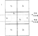
Fig. 1 and 2 is used to understand schematic diagram in kind of the present invention.Fig. 1 and 2 illustrates the cell array of forming a graph image, and each pixel is by a square expression.Array portion 1 shown in Fig. 1 and 2 comprises 13 row, and by " a " to " m " expression, each row comprises that nine pixels " 1 " are to " 9 ".The image section that illustrates comprises 3 kinds of colors.Color 1 by the dual crossing hachure illustrate, color 2 illustrates by single cross fork hachure, and color 3 is by there not being crosshatch to illustrate.By be applied in the suitable smoothing regulation that is described in more detail below by graphic OSD controller, this array can be shown as shown in Fig. 2.The diagonal border of the length between color 2 and 3 can be smoothed by the level and smooth pixel 6 of 1/4 size that produces color 2, and the narrow diagonal 4 of the color 1 within color 2 zones is by smoothed by the level and smooth pixel 8 that produces color 1.But,, just must can not produce level and smooth pixel, because importantly keep the profile of this former figure in this case if four elements 10 of color 3 are in the right zone of the lower floor of this array.Notice that for optimum, level and smooth element can be color any in palette.
As mentioned above, the color of each pixel in image array in the signal that receives by by one four bit vector defined, one of this vectors directed 16 input items in comprising the palette of representing the sort of color data.This input item in palette comprises by software and is pre-loaded to bit mode in this palette according to current request.This bit mode can be by receiver prestrain automatically, promptly can be by being provided to this palette in the data of television receiver from send the position received television signal.For example, each input item in palette can comprise the input item of one six bit, and wherein two bits are assigned to each value of red, green and blue colour content, and when being combined, these one-tenth are grouped into the display element of the sort of color.
Fig. 3 and 4 is memory layout schematic diagrames that explanation can make palette 20 used in this invention.In Fig. 3 and 4,16 input items in palette 20 are represented by the rectangle of correspondence, have hexadecimal from 0 to F address label.In Fig. 3, the data of expression color 1 (double cross hachure) are included among the input item C, the data of expression color 2 (single crosshatch) are included in two input items: input item 9 and input item 5, its reason is described in greater detail below, and the data of expression color 3 (not having crosshatch) are comprised in the input item 3.
In order to have a smoothing algorithm flexibly, i.e. operation and when not expecting to carry out inactive algorithm when level and smooth, the present invention is divided into two groups to 16 kinds of color input items in palette, is called the group of addresses 1 and 2 in Fig. 3 and 4 when the level and smooth edge of expectation.According to the present invention, only when by having one of color in group of addresses 1 simultaneously neighboring pixels be that the pixel of one of the color in group of addresses 2 forms an edge and just produces level and smooth pixel when detected.Otherwise do not carry out smoothing processing.By the color vector of describing Fig. 1 array is associated with the palette of arranging 20, can produce the demonstration of the expectation shown in Fig. 2 in Fig. 3.
Since color 2 (single crosshatch) and color 3 (not having crosshatch) form will be smoothed the edge, it is cornerwise edge, and form another not smoothed edge with color 3, i.e. pattern 10 in the lower right corner that shows, so be used for illustrating as Fig. 3 in the group of addresses 1 and group of addresses 2 that the input item of color 2 must be stored in palette 20.Specifically, for fear of the level and smooth pixel that produces around this pattern 10, around color 2 pixels of this pattern 10: j6, j8, k7,16 and 18 (in Fig. 2 with the asterisk mark) are pointed to the address 5 of palette 20 by vector representation in received signal.Because this input item is in group of addresses 2, so this osd controller in these pixels will not produce smoothly.The residue pixel of color 2 in received signal by the vector representation of the address 9 of pointing to palette 20.Because input item is in group of addresses 1, and the palette input item that is used for color 3 is in group of addresses 2, so will be produced among these pixels smoothly by this osd controller.Whole pixels of color 1 (dual crossing hachure) can be by the vector representation of the address C that points to palette 20 in received signal.Because this input item is a input item in group of addresses 1, so will produce level and smooth along the edge between the pixel of the pixel of color 1 and color 2.
In order to realize for comprising that the whole colors that are assigned to the array pixel carry out level and smooth flexibility, the color that is assigned to two group of addresses in palette 20 can resemble be caught shown in Figure 4 identical.In Fig. 4, the color that is designated as " m " to " t " is distributed to the address 7 to 0 of palette 20 respectively, and is assigned to the address F to 8 of palette 20 respectively.The number of color of use in any given image in such arrangement is eight.And might receive at this and comprise a shared control bit in data, can be used for starting or forbidding this smoothing algorithm, so that select the mode of operation of expectation.
As mentioned above, because the content of a graph image is unknown in advance, so this graphic OSD generator must be analyzed the data of reception, so that detect the position at edge and determine whether those edges will be smoothed.Fig. 5 is a schematic diagram, is used to understand operation of the present invention.
In Fig. 5, what illustrate is smaller portions of the array 1 among Fig. 1 and 2.Any independent pixel all is displayed on the display element as two adjacent scan line parts, and top scan line is called " odd number " row and the scan line of lower floor is called " even number " OK, and is shown in broken lines in Fig. 5.The data of presentation graphic image pixel are received and the color vector of representing different pixels is stored in the display-memory corresponding to the position of the pixel in graph image.This osd controller is retrieved these data from display-memory, and regulates this display element so that the change color in pixel border.
With reference to figure 5, pixel is by representing with the square of straight line frame.The pixel of current demonstration is designated as W, and the pixel on next-door neighbour right side is designated as X.Similarly, be adjacent to W and the pixel above the X and be appointed as Ya and Za respectively, and the pixel that is adjacent to below W and the X is appointed as Yb and Zb respectively.In order to produce a level and smooth pixel, this osd controller is regulated this display element, so that be created in the color change in the pixel unit of one of two scan lines of this pixel of composition.The level and smooth pixel dotted rectangle Re that level and smooth pixel dotted rectangle Ro that this is produced by expression even-line interlace row in Fig. 5 and expression odd-numbered scan lines produce illustrates.These level and smooth pixels have half height of standard pixel, but have the identical width as standard cell.They flatly are converted to half of width of standard pixel.This OSD generator will be regulated this display unit so that only just produce level and smooth pixel when the condition of describing below of determining is satisfied.
Fig. 6 (a) illustrates this condition that must exist to 6 (d), is used to produce two level and smooth pixel Ro or Re suitable one.For example, the conditional request shown in Fig. 6 (a) produces level and smooth pixel Ro:(a when the situation below existing) the palette address vector that is used for pixel X and Ya is identical, promptly pixel X is identical color (as the crosshatch demonstration) with Ya; (b) palette address that is used for color is at group of addresses 1 (Fig. 3 or 4); (c) palette address that is used for pixel W is in group of addresses 2.If the color of pixel X and Ya is identical, then show detected to bottom-right cornerwise edge and pixel W between pixel X and Ya from the upper left side.As mentioned above, if the group of addresses of the address that is used for pixel X and Ya in palette is in group of addresses 1, and the address that is used for pixel W is in group of addresses 2, then shows smoothly and will occur.In this case, a level and smooth pixel Ro who generation is had the color identical with Ya pixel (as showing) by crosshatch with X.Shown in Fig. 6 (a), this level and smooth pixel is edge between pixel X and Ya and pixel W smoothly.Otherwise just do not occur level and smooth.
Fig. 6 (b) is illustrated in rim detection and the smoothing processing of even-line interlace between the departure date.Conditional request shown in Fig. 6 (b) produces level and smooth pixel Re:(a when the situation below existing) palette address that is used for pixel X and Yb is identical; (b) address that is used for color vector is in group of addresses 1; (c) palette address that is used for pixel W is in group of addresses 2.If the color of pixel X and Yb is identical, show that then cornerwise edge from the upper right side to the lower left and the pixel W between pixel X and Yb is detected.As mentioned above, if the group of addresses of the input item that is used for pixel X and Yb in palette is in group of addresses 1, and the address that is used for pixel W is in group of addresses 2, then shows smoothly and will occur.In this case, a level and smooth pixel Re who generation is had the color identical with Yb pixel (as showing) by crosshatch with X.Shown in Fig. 6 (b), this level and smooth pixel is edge between pixel X and Yb and pixel W smoothly.Otherwise just do not occur level and smooth.
Fig. 6 (c) also relates to rim detection during odd-numbered scan lines and level and smooth, but what detect is the edge of other direction of those directions of being detected by Fig. 6 (a).Conditional request shown in Fig. 6 (c) produces level and smooth pixel Ro:(a when the situation below existing) the palette address vector that is used for pixel W and Za is identical; (b) palette address that is used for those pixels is in group of addresses 1; (c) palette address that is used for pixel X is in group of addresses 2.If the color of pixel W and Za is identical, show that then cornerwise edge from the upper right side to the lower left and the pixel X between pixel W and Za is detected.As mentioned above, if the group of addresses of the input item that is used for pixel W and Za in palette is in group of addresses 1, and the address that is used for pixel X is in group of addresses 2, then shows smoothly and will occur.In this case, a level and smooth pixel Ro who generation is had the color identical with the Za pixel with W.Shown in Fig. 6 (c), this level and smooth pixel is edge between pixel W and Za and pixel X smoothly.Otherwise just do not occur level and smooth.
Successively, Fig. 6 (d) also relates in the rim detection of even-line interlace between the departure date and level and smooth, but what detect is the edge of other direction of those directions of being detected by Fig. 6 (d).Conditional request shown in Fig. 6 (d) produces level and smooth pixel Re:(a when the situation below existing) the palette address vector that is used for pixel W and Zb is identical; (b) palette address that is used for these pixels is in group of addresses 1; (c) palette address that is used for pixel X is in group of addresses 2.If the color of pixel W and Zb is identical, then show detected to bottom-right cornerwise edge and pixel X between pixel W and Zb from the upper left side.As mentioned above, if the group of addresses of the input item that is used for pixel W and Zb in palette is in group of addresses 1, and the address that is used for pixel X is in group of addresses 2, then shows smoothly and will occur.In this case, a level and smooth pixel Re who generation is had the color identical with the Zb pixel with W.Shown in Fig. 6 (d), this level and smooth pixel is edge between pixel W and Za and pixel X smoothly.Otherwise just do not occur level and smooth.
With reference to figure 6 (a) and (c), visible during odd-numbered scan lines the address vector of the adjacent image point (Ya and Za) above only and the pixel in current scan line (W and X) compare.With reference to figure 6 (b) and (d), as seen compare at the address vector of even-line interlace adjacent image point (Yb and Zb) below only between the departure date and the pixel in current scan line (W and X).Therefore can be merged into two in four rules shown in Fig. 6 (a)-(d).First criterion relates to the detection of carrying out for the edge between pixel X and Y (at the Ya during the odd-numbered scan lines with at the Yb of even-line interlace between the departure date) and pixel W, and be illustrated in Fig. 6 (a) and (b) in.This criterion is: if (a) be used for the palette vector of pixel X is to be same as the palette vector that is used for pixel Y, (b) palette address that is used for these pixels is that the palette vector that is used for pixel W in group of addresses 1 neutralization (c) is in group of addresses 2, then produces a level and smooth pixel.Second criterion relates to the detection of carrying out for the edge between pixel W and Z (at the Za during the odd-numbered scan lines with at the Zb of even-line interlace between the departure date) and pixel X, and be illustrated in Fig. 6 (c) and (d) in.This criterion is: if (a) be used for the palette vector of pixel W is to be same as the palette vector that is used for pixel Z, (b) palette address that is used for these pixels is that the palette vector that is used for pixel X in group of addresses 1 neutralization (c) is in group of addresses 2, then produces a level and smooth pixel.
Refer again to Fig. 6, the level and smooth pixel Ro in embodiment is shown has identical width with Re, as pixel standard, full-scale, but only is the capable height of single scanning, and promptly 1/2 of a standard pixel height.Even level and smooth pixel Ro and Re have the width of a full-scale pixel, they also are to move with the width levels of half of actual size pixel ground, so partly overlap on actual size pixel same color, adjacent.Therefore half will be sightless for this of overlapping adjacent actual size pixel, and in fact not change demonstration.Such design according to the present invention can be simplified the hardware of realizing OSD generator needs.
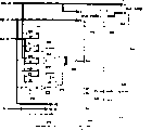
Fig. 7 is the block diagram according to the part of an osd controller 100 of the present invention.In Fig. 7, display random access memory 102 is coupled to an input of the one 4 bit shift register 104 to first output, and second output is coupled to an input of the 24 bit shift register 106.An output of first shift register 104 is coupled to an input of the 34 bit shift register 108, and is coupled to the X input of level and smooth logical circuit 112.An output of the 3rd shift register 108 is coupled to the W input of level and smooth logical circuit 112.An output of second shift register 106 is coupled to an input of the 44 bit shift register 110, and is coupled to the Z input of level and smooth logical circuit 112.An output of the 4th shift register 110 is coupled to the Y input of this level and smooth logical circuit 112.
An output of level and smooth logical circuit 112 is coupled to an input of palette memory 114.An output of palette 114 is coupled to the input of digital-to-analog (D/A) frequency converter and display device drive circuit 116.Other output of the branch of D/A converter and display driving circuit 116 produces colour signal R, G and B.These signals can combine with other R, G and B colour signal, for example combine with R, G and B colour signal from television reception circuit (not illustrating), and the television video frequency signal of representing a reception, and the display unit (also not illustrating) that can regenerate by the combination image of these signal indications is coupled in this combination.
Decoder 117 extracts for example closed caption data and graph data from the auxiliary informational content of vision signal VID IN.Signal VID IN can be anolog TV signals, for example NTSC compatible signal, or digital video signal, for example digital direct broadcasting satellite signal, for example a satellite-signal that is provided by the DirecTV* business.In a NTSC signal, auxiliary informational content can be included in the between-line spacing in the vertical blanking of NTSC compatible signal.In the digital video signal of a for example digital broadcast satellite signal, auxiliary informational content can be included in the data packets relevant with auxiliary inter-area traffic interarea.Some or all of decoder 117 and further feature shown in Figure 7 can be included in the integrated circuit, for example in microcontroller or the microcomputer.
In Fig. 7, the logical circuit 118 of packing into has an input equally, so that receive data, for example by the graph data of decoder 117 from an auxiliary informational content extraction.The output separately of the logical circuit 118 of packing into is coupled to the control input end that writes of corresponding display random access memory 102 and palette 114.Address ram and control logic circuit 120 are coupled to first and second address input end of control input end and display random access memory 102.An input end of clock is coupled to synchronously and the signal source (not illustrating) of the clock signal of received television signal.These clock signals comprise the synchronous composition and the control of a pixel (point) read clock of the TV signal that is synchronized with reception.Input end of clock is coupled to other input end of clock of branch of address ram and control logic circuit 120, is coupled to the first, second, third and the 4th shift register 104,106,108,110 respectively, and level and smooth logical circuit 112.This input end of clock can be coupled to other unit shown in Figure 7, or in other unit that this osd controller 100 does not illustrate.
In the operation, realize that wherein the television receiver of the OSD generator 100 of Fig. 7 receives the graphic OSD pictorial data (for example pixel color data and/or palette data) of the receipts TV signal of controlling oneself by decoder 117, and under the control of the logical one 18 of packing into, palette data is stored (promptly load) to palette 114, and the pixel color vector data of this OSD image of expression is stored into preposition in display random access memory 102.As mentioned above and as shown in Figure 6, OSD generator 100 shown in Figure 7 is analyzed the pixel color vector that is used for four neighboring pixels: W, X, Ya or Yb and Za or Zb.Therefore this OSD generator 100 is at odd number scan period request and pixel W, X and Ya four the 4 bit palette address vectors relevant with Za, or asks and pixel W, X and Yb four the 4 bit palette address vectors relevant with Zb during having even-line interlace at the same time.This address ram and control logic circuit 120 produce bit addresses signal A1 and the A2 more than two that is provided to this display random access memory 102.
The first address signal A1 is produced by one first counter (not illustrating) in address ram, and control logic circuit 120 carries out clock control by pixel clock signal.This Signal Regulation display random access memory 102 is so that present picture element is searched in its position from display random access memory 102.The second address signal A2 produces and regulates this display random access memory 102 by one second counter (also not illustrating) so that search pixel with the present picture element perpendicular abutment from its position this display random access memory 102.Address ram and control logic circuit 120 also respond the signal O/E from television receiver (not illustrating) synchronous circuit, and this signal O/E represents that current scan line is odd-numbered scan lines or even-line interlace row.During odd-numbered scan lines, the second address signal A2 regulates this display random access memory 102, so that search neighboring pixels vertically from the row on current line.Between the departure date, the second address signal A2 regulates this display random access memory 102 in even-line interlace, so that search neighboring pixels vertically from the row below current line.
Pixel data from current line produces at first output 01 of display random access memory 102, is coupled to first shift register 104.Pixel data (for odd-numbered scan lines is in the above, is below for the even-line interlace row) from suitably vertical adjacent scan lines produces at second output 02 of this display random access memory 102, is coupled to second shift register 106.First and second shift register 104 and 106 operation are for searching from the pixel of display random access memory 102.If directly the signal from display random access memory 102 outputs has sufficient drive capacity, and has correct timing, then can use to be different from the scheme of in Fig. 7, describing.For example, RAM output signal with suitable driving and timing characteristic can allow first and second shift register 104 and 106 to be omitted, and the output that allows this display random access memory 102 is directly coupled to the suitable input of third and fourth shift register 108 and 110, and level and smooth logical circuit 112.
First and second shift register 104 and 106 output produce level current, subsequently and corresponding vertical adjacent image point buffer memory with the streamline version.With reference to figure 5 and 6, these pixels are respectively X pixel and Z pixel (Za is used for odd-numbered scan lines, and Zb is used for the even-line interlace row).Third and fourth shift register 108 and 110 produces the pixel that has postponed a pixel time interval respectively.These pixels are W pixel and Y pixel (Ya is used for odd-numbered scan lines and Yb is used for the even-line interlace row).This first, second, third and the 4th shift register 104,106,108 and 110 cooperates, and extracts the pixel color vector data from the appropriate location display random access memory 102 and makes side by side available these data of this level and smooth logical circuit 112.
In the mode of describing among Fig. 6, level and smooth logical circuit 112 is analyzed through shift register 104,106,108 and 110 W from display random access memory 102, X, Y and Z pixel data, will describe in more detail below.112 generations of this level and smooth logical circuit are used for the control signal of palette 114.This control signal is regulated this palette, has received the colour signal that graph image adds the level and smooth pixel of whereabouts so that produce expression.Conversely, palette 114 responses are from the control signal of level and smooth logical circuit 112, so that produce suitable colour signal R, G and B.These colour signals can have been received R, G and the B signal combination of TV programme image with expression, so that produce the image of a combination.
Fig. 8 is partly with the data block form with partly with a more detailed schematic diagram shown in the logical form, represents an embodiment of level and smooth logical circuit 112 shown in Figure 7.In Fig. 8, thicker line is represented the multiple bit digital signal line, and thin line is represented one-bit digital holding wire or clock cable.Fig. 8 illustrates the gate structure of this level and smooth logical circuit 112, and this level and smooth logical circuit determines whether and produce one of this smooth unit Ro or Re (shown in Fig. 6) according to W, X, Y and Z pixel data.
In Fig. 8, W, X, Y receive four different bit palette address signals, W[3..0 with the Z input], X[3..0], Y[3..0] and Z[3..0], be used for W, X, Y and Z pixel.Whole four bits of X input are coupled to the second data input pin B of first multiplexer 202.An output of this first multiplexer 202 is coupled to an input I of latch 206.The output 0 of this latch 206 is coupled to the second data input pin B of second multiplexer 204.An output of second multiplexer 204 is coupled to an output of level and smooth logical circuit 112, and conversely, this output is coupled to the control input end (Fig. 7) of palette 114.
The minimum effective bit of W input WO is coupled to the first input end of first XOR (XOR) gate circuit 208, and the minimum effective bit ZO of Z input is coupled to second input of this first XOR gate 208.Similarly, bit W1 and Z1 are coupled to other input of branch of second XOR gate 210, and bit W2 and Z2 are coupled to other input of branch of the 3rd XOR gate 212, and bit W3 and Z3 are coupled to other input of branch of the 4th XOR gate 214.The highest significant bit Z3 of this Z pixel also is coupled to anti-phase output and (NAND) gate circuit 216.The highest significant bit of X pixel X3 also is coupled to an input of phase inverter 218.An output of phase inverter 218 is coupled to second input of NOT-AND gate 216.
The output of other output of the branch of the first, second, third and the 4th XOR gate 208-214 and NAND door 216 is coupled the corresponding input end of one five input or non-output (NOR) gate circuit 220.This first, second, third and the 4th XOR gate 208-214, NAND door 216, phase inverter 218 and NOR door 220 form first combinational logic circuit 250, this combinational logic circuit 250 extracts as four the bit W of input and the highest significant bit of Z pixel data signal and X pixel, and produces the output signal Rw of single bit from NOR door 220.
An output of NOR door 220 is coupled to the first input end of the NOR gate circuit 222 of one two input, and is coupled to a selection input of first multiplexer 202.An output of NOR door 220 is coupled to the D input of a d type flip flop 224.The Q output of this d type flip flop 224 is coupled to a selection control input end S of second multiplexer 204.
The structure of one second combinational logic circuit 270 is identical with the structure of first combinational logic circuit 250, and is only illustrated by data block in Fig. 8.X and Y input are coupled to first and second input respectively, and the highest significant position W3 of W input is coupled to one the 3rd input of this second combinational logic circuit 270.An output of this second combinational logic circuit 270 produces a signal Rx, is coupled to second input of NOR door 222.Clock signal input terminal is coupled to the input of second phase inverter 226.An output of this second phase inverter 226 is coupled to the input end of clock of d type flip flop 224 and the input end of clock of latch 206 respectively.
In the operation, combinational logic circuit comprises one four bit equality detectors (with dashed lines shows in Fig. 8) respectively to 250 and 270, form (250 circuit) by the first, second, third and the 4th XOR gate 208-214 and NOR door 220, be used for two pixel palette addresses; And the single bit comparator that forms by phase inverter 218, NAND door 216 and NOR door 220 (250 circuit), be used for determining whether being compared, and determine space neighboring pixels in group of addresses 2 (as shown in fig. 6) in the group of addresses of two pixels of group of addresses 1.With reference to this first combinational logic circuit 250, if the WO bit equates this Z0 bit, then this first XOR gate 208 produces logic ' a 0 ' signal, otherwise produces logic ' a 1 ' signal.This second, third and the 4th XOR gate 210-214 operate similarly.If the whole corresponding bit of W pixel and Z pixel is all the same, promptly the W pixel is identical with the color of Z pixel, and then whole four XOR gate 208-214 produce logic ' 0 ' signal.
Again with reference to figure 3 and 4, the highest significant position that is used for the palette address of a pixel is the indication of the group of addresses that belongs to of this pixel.If the highest significant position of palette address (bit 3) is logic ' a 0 ' signal, then this address is in the scope of 0-7, and this pixel is in group of addresses 2.If the highest significant position of palette address is logic ' a 1 ' signal, then this address is in the scope of 8-F, and pixel is in group of addresses 1.
Again with reference to figure 8, as mentioned above, be in group of addresses 2 and the palette address of W and Z pixel is in group of addresses 1 if be used for the palette address of X pixel, then smoothly will occur, otherwise not occur level and smooth.When the highest significant position Z3 of Z pixel was a logic ' 1 ' signal, the cooperation of phase inverter 218 and NAND door 216 produced logic ' a 0 ' signal, and the palette address that shows the X pixel is in group of addresses 2.As mentioned above, this show will occur level and smooth.Otherwise the cooperation of phase inverter 218 and NAND door 216 produces logic ' a 1 ' signal.
When the signal from the first, second, third and the 4th XOR gate 208-214 and NAND door 216 all is logic ' 0 ' signal, NOR door 220 produces logic ' a 1 ' signal, show that W and Z pixel are identical colors and in group of addresses 1, and the palette address of X pixel is in group of addresses 2.This is corresponding to during the odd-numbered scan lines of Fig. 6 (c) and the adjusting of Fig. 6 (d) even-line interlace between the departure date.Show will produce for a pixel carry out level and smooth.Otherwise NOR door 220 produces logic ' a 0 ' signal, shows not producing pixel level and smooth.
When the signal from the first, second, third and the 4th XOR gate (not illustrating) and its NAND door (also not illustrating) all is that logic is ' during 0 ' signal, combinational logic circuit 270 is operated similarly and is produced logic ' 1 ' signal Rx, show that this X and Y pixel are identical colors and in group of addresses 1, and show that the palette address of W pixel is in group of addresses 2.This corresponding to shown in Fig. 6 (a) during the odd-numbered scan lines and shown in Fig. 6 (b) in the condition of even-line interlace between the departure date.This shows will produce a level and smooth pixel.Otherwise NOR door (also not illustrating) produces a logic, and ' 0 ' signal shows and will not produce level and smooth pixel.Therefore, combinational logic circuit 250 and 270 detects the appearance at the edges in this graphic OSD image, and determines whether level and smooth this edge of the level and smooth pixel that will produce.
When needs, the remainder of the level and smooth logical circuit 112 shown in Fig. 8 will be operated and produce this level and smooth pixel.Again with reference to figure 6, ' during 1 ' Rw signal, level and smooth pixel has the color the same with the W pixel when the logic that is produced by combinational logic circuit 250 (Fig. 6 (c) and (d)).' during 1 ' Rx signal, level and smooth pixel has the color the same with the X pixel when produced logic by combinational logic circuit 270.When the Rw signal is that a logic is ' during 1 ' signal, first multiplexer 202 is conditioned so that the W input is coupled to its output, and when the Rw signal is that ' during 0 ' signal, this first multiplexer 202 is conditioned so that the X input is coupled to its output a logic.Therefore, if desired, the output of first multiplexer 202 will produce a signal of representing the color that level and smooth pixel will have.
Fig. 9 is the waveform schematic diagram of operation that is used to understand the remainder of level and smooth logical circuit 112 shown in Figure 8.In the example of describing by the waveform among Fig. 9, illustrate and be used for during a pixel, to become effectively suitable adjusting.This corresponding to adjacent ring around pixel h7 (Fig. 1).The highest waveform DC in Fig. 9 is the input end of clock of level and smooth logical circuit 112 (Fig. 8).If can see from Fig. 9, produce new pixel in the rising edge of this image point clock signal DC.The second waveform DC* in Fig. 9 is the DC from the inversion image point clock of second phase inverter 226.
The 3rd waveform is W and Z pixel data stream.The pixel of each sequence in pixel data stream is represented by a rectangle.Hexadecimal number in rectangle is to describe the palette address of the color of this pixel, the corresponding pixel in the image shown in Figure 1 of the coordinate representation under pixel some illustrate.Under general condition, two pixel datas stream W and Z do not need identical.But, in this example, be identical at the W and the Z pixel data stream of the cell array of Fig. 1, and in Fig. 9, represent by single waveform.The 4th waveform is to flow with the X pixel data shown in W and the Z pixel data stream same way as.
The 5th waveform is the output signal Rw from NOR door 220 (Fig. 8).The 6th waveform is the output signal Sw from d type flip flop 224.The 7th waveform is the palette address signal that is provided to palette 114 from the output of second multiplexer 204.
Standard operation illustrates during promptly not producing the first complete pixel that operates in Fig. 9 of level and smooth pixel.During standard operation, all be logic ' 0 ' signal from the output signal of first and second combinational logic circuit 250 and 270.Therefore, the output signal from NOR door 222 is logic ' a 1 ' signal.Logic ' 1 ' signal from NOR door 222 passes through d type flip flop 224 at the rising edge of the image point clock signal DC* of paraphase.Response is from the logic ' 1 ' signal of the delay of the Q output of d type flip flop 224, and this second multiplexer is coupled its first input end A that delivers the signal of representing the W pixel to its output.Therefore, during standard operation, the signal that is provided to this palette 114 is a signal of representing this W pixel with pipeline system.
For following explanation, suppose that current scan line is an odd-numbered scan lines.With reference to the waveform in Fig. 9 with at the image section shown in Fig. 1 and Fig. 6 (c), during the second complete pixel shown in Figure 9, for W and Z pixel, the palette address both is C, be color 1 (dual crossing hachure), and for the X pixel, this palette address is 5, i.e. color 2 (single crosshatch).With reference to figure 1, when appearing at current pixel W and being pixel h6, subsequently pixel X be h7 and suitable vertical neighboring pixels Z from this row above current line, and be pixel g7.This position is gone out by the bold box in Fig. 1, and corresponding to Fig. 6 (c).
Because W has identical palette address with the Z pixel, i.e. address C is so this first, second, third and the 4th XOR gate 208,210,212 and 214 all produces logic ' 0 ' signals.Because W and Z pixel are in group of addresses 1 (being address C) and pixel X is in group of addresses 2 (being address 5), so this NAND door 216 also produces logic ' a 0 ' signal.Therefore, for signal Rw, NOR door 220 produces logic ' a 1 ' signal, shown in Fig. 9.As mentioned above, regulate this first multiplexer 202 so that the W pixel signal is coupled to its output.Latch 206 is by the pixel of paraphase (image point) clock DC* clock control, and half pixel cycle lagged behind.The W pixel signal remains on the output of latch, up to the centre in pixel cycle subsequently.
Side by side, NOR door 222 produces logic ' a 0 ' signal.In the forward position of subsequently inversion Dot Clock signal DC*, from the logic ' 0 ' signal of NOR door 222 by clock control, by d type flip flop 224, as waveform Sw shown in Figure 9.This second multiplexer of this Sw Signal Regulation is so that the B input that it is coupled to latch 206 output and has a value C is coupled to its output.The Sw signal keeps the logic of a signal up to the next forward position of the image point clock signal DC* of paraphase, in this time, is logic ' 1 ' signals from the output of NOR door 222.This will regulate second multiplexer so that the signal from W pixel input is coupled to its output, and recover standard operation.
The result is that the color that is stored in the level and smooth pixel of address C in the palette is become the next pixel of the color that is stored in address 5 apart from (half-way) by " extension " half.Therefore single smooth unit produces, and should produce pattern shown in the part of Fig. 2, the sliding part of the circle of corresponding diagram 1 and shown in Fig. 6 (c).
Show in figure that illustrates in the above and corresponding detailed description the in detail and that describe is an embodiment that can be created in the favourable level and smooth edge of graphic OSD in showing.But those skilled in the art will be understood, and can design and make other embodiment, and same the realization strengthens for the video of the osd image data that receive.
Claims (12)
1. a graphic screen shows (OSD) system, comprising:
A memory, the second group of memory location that has first group of memory location of the data that are used for first group of color of storage representation and have the data that are used for second group of color of storage representation, the data of representing first color are stored in each group memory location among first and second group memory location;
A decoder, be used for extracting the graphic screen display image representative data of the auxiliary informational content that is included in a TV signal, this graphic screen display image representative data comprises the data that are illustrated in the location address in this memory, is used for showing the color at the pixel of a graphic screen display image;
An edge detector is used to handle this display image screen representative data, so that detect an edge in the graphic screen display image between second group of pixel of the first group of pixel of first color and second color; And
An edge-smoothing device that is coupled to this decoder and this edge detector, be used for producing the signal that expression has the display image screen of a smooth edges in order to respond first and second represented color of data of utilizing first scheme among the memory location be stored in first and second group, and be used for a signal utilizing first and second the represented color of data be stored in the alternative plan among first and second group memory location and produce the display image screen that expression do not have a smooth edges in order to respond, produce described smooth edges and detect the edge that the pixel that utilizes one of color with second group of memory location forms to respond described edge detector.
2. according to the system of claim 1, wherein first scheme of first and second group memory location is stored in first and second group not represented described first and second color of data on the same group among memory location corresponding to utilization, and the alternative plan of first and second group memory location is stored in phase first and second represented color of data on the same group among first and second group memory location corresponding to utilization.
3. according to the system of claim 2, wherein:
This graphic screen display image comprises a cell array, and this graphic screen display image representative data comprises the data value that is illustrated in the corresponding pixel in this graphic screen display image;
Described system also comprises the circuit that is coupled to decoder, is used for producing simultaneously expression and is included in a group among first and second group of pixels and forms the corresponding data value of two adjacent image points at described edge and expression is included in another group among first and second group of pixels and form the corresponding data value of an adjacent pixel of pixels with these two edges; With
Be used to determine when the circuit at the level and smooth detected edge of expectation, comprise:
A comparator, be coupled to this data value and produce circuit, be used for these two edges of expression being formed the data value of pixel and representing that the data value that forms the adjacent described pixel of pixel with this two edges compares, and when these two edges of expression form the data value of pixels and data value that two edges of expression and this form the adjacent described pixel of pixels and satisfy a predetermined criterion, produce a signal; With
Be coupled to the circuit that this data value produces circuit and this comparator, be used for when the data value that data value and two edges of expression and this of these two edges formation pixels of expression form the adjacent described pixel of pixel satisfies described predetermined criterion, producing a signal of representing level and smooth pixel.
4. according to the system of claim 3, the circuit that wherein is coupled to this data value generation circuit and this comparator produces has the level and smooth pixel representation signal that these two edges produce the data value of one of pixels.
5. according to the system of claim 3, wherein each pixel in this cell array has predetermined height and width, and described generation represents that the circuit of the signal of level and smooth pixel comprises the circuit that is coupled to this data value generation circuit and this comparator, be used to produce level and smooth pixel representation signal, described signal have the pixel in the described cell array height half, the width of the pixel in the described cell array and by half of the pixel width in the described cell array of skew.
6. according to the system of claim 3, wherein:
Described memory comprises a palette that is coupled to this decoder and this edge-smoothing device, is used for producing the signal of color of the pixel of the display image screen that is illustrated in regeneration;
This graphic screen display image representative data value is to point to the address of the input item in the described palette, and wherein said address is divided into first and second group of addresses corresponding to first and second group memory location;
This comparator is the group of addresses of the data value of two edges formation of expression pixel and represent that the group of addresses that forms the data value of pixel neighboring pixels with these two edges compares, and the group of addresses of data value that forms pixels at these two edges of expression is in one of first and second group of addresses and two edges of expression and this when forming in group of addresses another group of addresses among first and second group of addresses of data value of the adjacent described pixel of pixels, generation predetermined criterion index signal.
7. according to the system of claim 6, wherein:
Described data value comprises that two edges of expression form the graphic screen display image representative data value of pixel and the data value that two edges of expression and this form the pixel neighboring pixels, each described data value is the multiple bit digital data value with highest significant position, and this palette address be divided into one wherein highest significant position be first group of addresses of logic ' 1 ' signal and one wherein highest significant position be second group of addresses of logic ' 0 ' signal; With
This comparator comprise be used for two edges of expression form one of pixels data value highest significant position and form the circuit that the highest significant position of the adjacent described pixel of pixel compares with two edges.
8. one kind is used for producing the method that expression regeneration graphic screen shows the signal of (OSD) image, may further comprise the steps:
The storage of first group of color that expression is comprised first kind of color is in first group of memory location;
The storage of second group of color that expression is comprised first kind of color is in second group of memory location;
From the auxiliary informational content of a TV signal, extract graphic screen display image representative data, this graphic screen display image representative data comprises the data of the address of representing the memory location, is used for showing the color at the pixel of a graphic screen display image;
Handle this graphic screen display image representative data, so that detect an edge in the graphic screen display image between second group of pixel of the first group of pixel of first color and second color; And
To utilize first and second the represented color of data in first scheme be stored among first and second group memory location and produce the signal that expression has the graphic screen display image of a smooth edges in order to respond, and in order to respond a signal that utilizes first and second the represented color of data in the alternative plan be stored among first and second group memory location and produce the graphic screen display image that expression do not have a smooth edges, produce described smooth edges and detect the edge that utilizes the pixel formation with one of first group of color in the memory location with response, adjacent image point has one of second group of color among the memory location simultaneously.
9. method according to Claim 8, wherein: first scheme of first and second group memory location is stored in represented described first and second color of data in not on the same group the memory location of first and second group among memory location corresponding to utilization, and the alternative plan among first and second group memory location is stored in first and second represented color of data in the same group of memory location among first and second group memory location corresponding to utilization.
10. according to the method for claim 9, wherein this graphic screen display image comprises a cell array, and this graphic screen display image representative data comprises the data value of the corresponding pixel in the described graphic screen displayed image of expression; And described method also comprises the step that determines whether to expect to produce a smooth edges, and described step may further comprise the steps:
The data value of two adjacent image points at an edge of expression formation and one three pixel adjacent with these two edges formation pixels are compared; And
If these data values satisfy a predetermined criterion, then determine the edge that expectation is level and smooth.
11. according to the method for claim 10, wherein said data value is the address of pointing to the input item in the palette, comprises the data of the desired color of representing each pixel; The address of this palette input item is divided into first and second group of addresses corresponding to first and second group memory location; And the step of this comparing data value may further comprise the steps:
The group of addresses of the group of addresses of the data value of two adjacent image points of expression with the data value of expression the 3rd pixel compared; And
If representing the data value of these two adjacent image points is in one of first and second group of addresses, and represent that the data value of the 3rd pixel is in the another one group of addresses of first and second group of addresses, determine that then expectation produces a level and smooth edge.
12. method according to claim 11, wherein each pixel in this cell array has a predetermined height and width, and this smooth edges produces step and comprises the step that produces a level and smooth pixel, and this level and smooth pixel has half height and half width of the pixel in this cell array.
Applications Claiming Priority (4)
| Application Number | Priority Date | Filing Date | Title |
|---|---|---|---|
| US2699696P | 1996-10-07 | 1996-10-07 | |
| US60/026,996 | 1996-10-07 | ||
| GB9621255.0 | 1996-10-11 | ||
| GBGB9621255.0A GB9621255D0 (en) | 1996-10-11 | 1996-10-11 | Rounding of features of graphic elements displayed on the television screen |
Publications (2)
| Publication Number | Publication Date |
|---|---|
| CN1240087A CN1240087A (en) | 1999-12-29 |
| CN1130075C true CN1130075C (en) | 2003-12-03 |
Family
ID=26310216
Family Applications (1)
| Application Number | Title | Priority Date | Filing Date |
|---|---|---|---|
| CN97180331A Expired - Fee Related CN1130075C (en) | 1996-10-07 | 1997-10-07 | Graphical on-screen display system |
Country Status (8)
| Country | Link |
|---|---|
| US (1) | US6339451B1 (en) |
| EP (1) | EP0929971B1 (en) |
| JP (1) | JP2001502481A (en) |
| KR (1) | KR100472909B1 (en) |
| CN (1) | CN1130075C (en) |
| AU (1) | AU4645897A (en) |
| DE (1) | DE69718804T2 (en) |
| WO (1) | WO1998016063A1 (en) |
Families Citing this family (13)
| Publication number | Priority date | Publication date | Assignee | Title |
|---|---|---|---|---|
| US6469753B1 (en) | 1996-05-03 | 2002-10-22 | Starsight Telecast, Inc. | Information system |
| US6678006B1 (en) * | 1998-01-07 | 2004-01-13 | Ati Technologies, Inc. | Method and apparatus for video processing that includes sub-picture scaling |
| KR20010097454A (en) * | 2000-04-24 | 2001-11-08 | 윤종용 | Osd(on screen display) object display method and apparatus |
| US8391649B2 (en) * | 2003-08-01 | 2013-03-05 | Texas Instruments Incorporated | Image filter method |
| KR100601702B1 (en) * | 2004-09-30 | 2006-07-18 | 삼성전자주식회사 | OSD data display control method and apparatus therefor |
| US7667682B2 (en) * | 2004-11-25 | 2010-02-23 | Sanyo Electric Co., Ltd. | Display |
| JP4114668B2 (en) * | 2005-03-25 | 2008-07-09 | エプソンイメージングデバイス株式会社 | Display device |
| JP4650056B2 (en) * | 2005-03-30 | 2011-03-16 | エプソンイメージングデバイス株式会社 | Display device |
| KR100717050B1 (en) * | 2005-11-05 | 2007-05-14 | 삼성전자주식회사 | Apparatus and method for generating animated graphic image, and effect handler used thereto |
| US20080106646A1 (en) * | 2006-11-06 | 2008-05-08 | Media Tek Inc. | System, apparatus, method, and computer program product for generating an on-screen display |
| JP4845825B2 (en) * | 2007-07-25 | 2011-12-28 | 株式会社 日立ディスプレイズ | Multicolor display device |
| JP2011059216A (en) * | 2009-09-08 | 2011-03-24 | Renesas Electronics Corp | Display device and display control method |
| US9516389B1 (en) * | 2010-12-13 | 2016-12-06 | Pixelworks, Inc. | On screen display detection |
Family Cites Families (9)
| Publication number | Priority date | Publication date | Assignee | Title |
|---|---|---|---|---|
| JPS6145279A (en) | 1984-08-09 | 1986-03-05 | 株式会社東芝 | Smoothing circuit |
| US4953027A (en) * | 1989-04-24 | 1990-08-28 | Motorola Inc. | OSD in a TV receiver including a window, smoothing and edge enhancing |
| US5293579A (en) | 1992-02-18 | 1994-03-08 | Ray Dream, Inc. | Method and apparatus for smoothing jagged edges in a graphics display |
| JP2975796B2 (en) * | 1993-02-10 | 1999-11-10 | 三洋電機株式会社 | Character display device |
| DE69423418T2 (en) | 1993-11-02 | 2000-09-21 | Texas Instruments Inc | Device and method for graphic data for television receivers |
| JPH07334669A (en) * | 1994-06-07 | 1995-12-22 | Matsushita Electric Ind Co Ltd | Method and device for graphic processing |
| DE19636949A1 (en) * | 1996-09-11 | 1998-03-12 | Siemens Ag | Method for the detection of edges in an image signal |
| US6148115A (en) * | 1996-11-08 | 2000-11-14 | Sony Corporation | Image processing apparatus and image processing method |
| US5966475A (en) * | 1997-02-20 | 1999-10-12 | Hewlett-Packard Company | System for enlarging and smoothing textual characters |
-
1997
- 1997-10-07 JP JP10517533A patent/JP2001502481A/en not_active Ceased
- 1997-10-07 AU AU46458/97A patent/AU4645897A/en not_active Abandoned
- 1997-10-07 WO PCT/US1997/016273 patent/WO1998016063A1/en active IP Right Grant
- 1997-10-07 DE DE69718804T patent/DE69718804T2/en not_active Expired - Fee Related
- 1997-10-07 EP EP97945206A patent/EP0929971B1/en not_active Expired - Lifetime
- 1997-10-07 CN CN97180331A patent/CN1130075C/en not_active Expired - Fee Related
- 1997-10-07 US US09/254,961 patent/US6339451B1/en not_active Expired - Lifetime
- 1997-10-07 KR KR10-1999-7002971A patent/KR100472909B1/en not_active IP Right Cessation
Also Published As
| Publication number | Publication date |
|---|---|
| AU4645897A (en) | 1998-05-05 |
| US6339451B1 (en) | 2002-01-15 |
| EP0929971A1 (en) | 1999-07-21 |
| DE69718804T2 (en) | 2003-09-11 |
| KR100472909B1 (en) | 2005-03-07 |
| JP2001502481A (en) | 2001-02-20 |
| WO1998016063A1 (en) | 1998-04-16 |
| EP0929971B1 (en) | 2003-01-29 |
| KR20000048934A (en) | 2000-07-25 |
| CN1240087A (en) | 1999-12-29 |
| DE69718804D1 (en) | 2003-03-06 |
Similar Documents
| Publication | Publication Date | Title |
|---|---|---|
| CN1130075C (en) | Graphical on-screen display system | |
| US5473383A (en) | Mechanism for controllably deinterlacing sequential lines of video data field based upon pixel signals associated with three successive interlaced video fields | |
| US5521644A (en) | Mechanism for controllably deinterlacing sequential lines of video data field based upon pixel signals associated with four successive interlaced video fields | |
| EP0408834B1 (en) | On screen display in a TV receiver | |
| JP3818662B2 (en) | Image processing system having a single frame buffer | |
| US5850471A (en) | High-definition digital video processing system | |
| JP2009534931A (en) | Shared memory multi-video channel display apparatus and method | |
| CN1048132C (en) | Graphics sub-displays for digital television receivers | |
| JP5217037B2 (en) | Shared memory multi-video channel display apparatus and method | |
| US4771275A (en) | Method and apparatus for assigning color values to bit map memory display locations | |
| CN1032893A (en) | Television receiver with in-memory switching signal | |
| JP5363694B2 (en) | Window detection | |
| US8964117B2 (en) | Single-pass motion adaptive deinterlacer and method therefore | |
| US7710435B2 (en) | Method and apparatus for generating visual effects | |
| CN1076323A (en) | Produce the equipment of figure according to canned data | |
| CN101461233A (en) | Shared memory multi video channel display apparatus and methods | |
| JPH08297481A (en) | Graphic image display device | |
| JP2004236012A (en) | Image processing method and device thereof | |
| AU720754B2 (en) | A method of smoothing bitmapped characters | |
| JPS59197082A (en) | Display circuit | |
| JPS6224298A (en) | Pixel rounding processing method and apparatus | |
| JPH0683394B2 (en) | Multi-screen display control circuit and video equipment including the same | |
| JPH05300446A (en) | Master/slave picture display circuit | |
| JPH11219158A (en) | Video overlay device | |
| JPH0380293A (en) | Display device |
Legal Events
| Date | Code | Title | Description |
|---|---|---|---|
| C06 | Publication | ||
| PB01 | Publication | ||
| C10 | Entry into substantive examination | ||
| SE01 | Entry into force of request for substantive examination | ||
| C14 | Grant of patent or utility model | ||
| GR01 | Patent grant | ||
| C19 | Lapse of patent right due to non-payment of the annual fee | ||
| CF01 | Termination of patent right due to non-payment of annual fee |