CN112912356B - Method for manufacturing silicon nitride substrate and silicon nitride substrate - Google Patents
Method for manufacturing silicon nitride substrate and silicon nitride substrate Download PDFInfo
- Publication number
- CN112912356B CN112912356B CN201980070845.9A CN201980070845A CN112912356B CN 112912356 B CN112912356 B CN 112912356B CN 201980070845 A CN201980070845 A CN 201980070845A CN 112912356 B CN112912356 B CN 112912356B
- Authority
- CN
- China
- Prior art keywords
- silicon nitride
- nitride substrate
- substrate
- powder
- less
- Prior art date
- Legal status (The legal status is an assumption and is not a legal conclusion. Google has not performed a legal analysis and makes no representation as to the accuracy of the status listed.)
- Active
Links
Images


Classifications
-
- C—CHEMISTRY; METALLURGY
- C04—CEMENTS; CONCRETE; ARTIFICIAL STONE; CERAMICS; REFRACTORIES
- C04B—LIME, MAGNESIA; SLAG; CEMENTS; COMPOSITIONS THEREOF, e.g. MORTARS, CONCRETE OR LIKE BUILDING MATERIALS; ARTIFICIAL STONE; CERAMICS; REFRACTORIES; TREATMENT OF NATURAL STONE
- C04B35/00—Shaped ceramic products characterised by their composition; Ceramics compositions; Processing powders of inorganic compounds preparatory to the manufacturing of ceramic products
- C04B35/515—Shaped ceramic products characterised by their composition; Ceramics compositions; Processing powders of inorganic compounds preparatory to the manufacturing of ceramic products based on non-oxide ceramics
- C04B35/58—Shaped ceramic products characterised by their composition; Ceramics compositions; Processing powders of inorganic compounds preparatory to the manufacturing of ceramic products based on non-oxide ceramics based on borides, nitrides, i.e. nitrides, oxynitrides, carbonitrides or oxycarbonitrides or silicides
- C04B35/584—Shaped ceramic products characterised by their composition; Ceramics compositions; Processing powders of inorganic compounds preparatory to the manufacturing of ceramic products based on non-oxide ceramics based on borides, nitrides, i.e. nitrides, oxynitrides, carbonitrides or oxycarbonitrides or silicides based on silicon nitride
- C04B35/593—Shaped ceramic products characterised by their composition; Ceramics compositions; Processing powders of inorganic compounds preparatory to the manufacturing of ceramic products based on non-oxide ceramics based on borides, nitrides, i.e. nitrides, oxynitrides, carbonitrides or oxycarbonitrides or silicides based on silicon nitride obtained by pressure sintering
-
- C—CHEMISTRY; METALLURGY
- C04—CEMENTS; CONCRETE; ARTIFICIAL STONE; CERAMICS; REFRACTORIES
- C04B—LIME, MAGNESIA; SLAG; CEMENTS; COMPOSITIONS THEREOF, e.g. MORTARS, CONCRETE OR LIKE BUILDING MATERIALS; ARTIFICIAL STONE; CERAMICS; REFRACTORIES; TREATMENT OF NATURAL STONE
- C04B35/00—Shaped ceramic products characterised by their composition; Ceramics compositions; Processing powders of inorganic compounds preparatory to the manufacturing of ceramic products
- C04B35/622—Forming processes; Processing powders of inorganic compounds preparatory to the manufacturing of ceramic products
- C04B35/64—Burning or sintering processes
-
- H—ELECTRICITY
- H05—ELECTRIC TECHNIQUES NOT OTHERWISE PROVIDED FOR
- H05K—PRINTED CIRCUITS; CASINGS OR CONSTRUCTIONAL DETAILS OF ELECTRIC APPARATUS; MANUFACTURE OF ASSEMBLAGES OF ELECTRICAL COMPONENTS
- H05K1/00—Printed circuits
- H05K1/02—Details
- H05K1/03—Use of materials for the substrate
Landscapes
- Engineering & Computer Science (AREA)
- Chemical & Material Sciences (AREA)
- Ceramic Engineering (AREA)
- Manufacturing & Machinery (AREA)
- Materials Engineering (AREA)
- Structural Engineering (AREA)
- Organic Chemistry (AREA)
- Inorganic Chemistry (AREA)
- Microelectronics & Electronic Packaging (AREA)
- Ceramic Products (AREA)
Abstract
A method for producing a silicon nitride substrate, characterized in that a plurality of green sheets containing silicon nitride powder and a sintering aid are stacked and sintered with a separating material interposed therebetween, and then separated to obtain a plurality of silicon nitride sintered bodies, whereby a silicon nitride substrate is obtained from the silicon nitride sintered bodies, and the separating material contains silicon nitride powder. The obtained silicon nitride substrate does not contain boron nitride powder on the surface, and therefore has excellent thermal cycle properties when bonded to copper. The specific surface area of the separating material measured by BET method was 1m 2 Above/g and 20m 2 And/g or less, wherein 50% of the particles have a particle diameter D50 of 20 μm or less, and an oxygen content of 0.3 wt.% or more and less than 2 wt.% as measured by a laser diffraction scattering method, by mixing the separating material at 0.1mg/cm 2 Above and 3mg/cm 2 The following coating amounts were applied to the green sheet surface to obtain a silicon nitride substrate having a thermal conductivity of 80W/(mK) or more at room temperature and a 4-point bending strength of 800MPa or more at room temperature.
Description
Technical Field
The present invention relates to a method for producing a silicon nitride substrate used for an insulating substrate and a circuit substrate, and a silicon nitride substrate produced by the production method.
Background
In recent years, various ceramic (sintered body) substrates have been widely used as substrates for semiconductor modules and structural members. For example, a substrate for a semiconductor module on which a semiconductor element having high power and a large heat generation amount is to be mounted is required to have high mechanical strength, high thermal conductivity, and high electrical insulation. These characteristics of a nitride sintered body such as aluminum nitride and silicon nitride are excellent, and these nitride sintered body substrates are widely used.
A nitride sintered body as a base of a nitride substrate is obtained by sintering a nitride (AlN, si) 3 N 4 Etc.) the green sheet containing the powder as a main component is produced by sintering the green sheet in a nitrogen atmosphere at a high temperature. In this case, the following manufacturing method is generally adopted: a large-area nitride sintered body is produced, and a plurality of substrates having a desired size are cut out from the sintered body. The sintering is performed using an electric furnace or the like, but in order to reduce the manufacturing cost, a method of stacking a plurality of green sheets and sintering them to obtain a plurality of nitride sintered bodies at the same time may be used.
In this sintering, in order to prevent adhesion between the stacked nitride sintered bodies, the green sheets to be made into the nitride sintered bodies are stacked after the surface is coated with a release material. After sintering, the plurality of nitride sintered bodies can be separated by the separation material.
Since a sintered nitride body such as aluminum nitride and silicon nitride needs to be sintered at a high temperature of 1600 ℃ or higher, boron Nitride (BN) powder stable at a high temperature of not less than the sintering temperature is widely used as a separator in order to improve the peeling property between the sintered nitride bodies.
As described above, since the BN powder is sintered while being held between the nitride sintered bodies, the BN powder must not be deformed by restraining the nitride sintered bodies or reacting with the nitride sintered bodies during sintering. Therefore, it is necessary to select the properties of the BN powder to be used, the process for coating the BN powder, and other production conditions.
Patent document 1 discloses a method for producing a plate-like ceramic sintered body, in which a plurality of green sheets are stacked with a release material made of fine particles having high heat resistance interposed therebetween, and fired while being pressed in the stacking direction of the stacked green sheets. In this invention, it is described that warpage and cracks during sintering can be prevented, and the stacked sheets can be easily peeled without being fixed. However, there is no description about a silicon nitride thin plate as a ceramic sintered body, and there is no description about the use of silicon nitride powder as a release material in the production of a silicon nitride thin plate.
Patent document 3 describes a method for producing a silicon nitride substrate, which is formed from a silicon nitride sintered body containing silicon nitride particles and a sintering aid containing at least magnesium oxide, the silicon nitride particles containing columnar crystal particles having a short diameter a of 0.5 to 5 μm and a ratio (B/a) of long diameter B to short diameter a of 2 or more in an area ratio of 30% or more, the arithmetic average roughness Ra of the substrate surface being 0.3 to 2 μm or more, the ratio of BN remaining on the substrate surface to silicon nitride being greater than 6.5x10 in terms of the ratio (B/Si) of fluorescent X-ray intensity of B to fluorescent X-ray intensity of Si, and a silicon nitride substrate, and a circuit board using the silicon nitride substrate -5 And is 300X 10 -5 The following is given. However, when the residual amount of boron nitride, which is a separating material remaining on the surface of the silicon nitride substrate, is in an appropriate range, the heat cycle resistance at the time of joining copper plates is improved, but the bending strength is 750MPa to 830 MPa.
Prior art literature
Patent literature
Patent document 1: japanese patent laid-open No. 1-87574
Patent document 2: japanese patent laid-open publication No. 2011-178598
Patent document 3: japanese patent laid-open publication No. 2011-216577
Patent document 4: international publication No. 2013/146713
Disclosure of Invention
Problems to be solved by the invention
According to these prior arts, boron nitride as a separating material is applied to the surface of a ceramic green sheet, whereby a silicon nitride substrate having good peelability and less deformation can be obtained after stacking and sintering a plurality of green sheets, but since boron nitride as a separating material remains on the substrate surface, problems occur in heat cycle resistance when joining copper plates, and improvement is desired.
In addition, in these conventional techniques, the semiconductor modules having an increasing amount of heat generation in recent years often have insufficient thermal conductivity and mechanical properties, and in particular, it is further desired to stably secure heat release up to a high temperature region during operation, and under this current situation, there is a problem of insufficient performance in terms of both thermal conductivity and mechanical properties.
For example, a method of reducing the coating amount of a Boron Nitride (BN) separating material on the surface of a green sheet, a method of forcibly removing a BN separating material by strengthening the processing conditions such as polishing or honing (honing) the surface of a silicon nitride sintered body, or the like, is employed to improve the heat cycle resistance, so that the B/Si fluorescent X-ray intensity ratio indicating the ratio of BN remaining on the surface of a substrate to silicon nitride is 5×10 -5 In the following cases, defects remain on the surface of the silicon nitride sintered body or damage occurs, and the bending strength thereof is also reduced.
In patent document 3, in a silicon nitride substrate formed of a silicon nitride sintered body containing silicon nitride particles and a sintering aid containing at least magnesium oxide, the silicon nitride particles contain columnar crystal particles having a short diameter a of 0.5 to 5 μm and a ratio (b/a) of a long diameter b to a short diameter a of 2 or more in an area ratio of 30% or more, and the substrate surfaceThe arithmetic average roughness Ra of (2) is 0.3-2 mu m, and the ratio of the fluorescent X-ray intensity of B to the fluorescent X-ray intensity of Si (B/Si) is greater than 6.5X10 -5 And is 300X 10 -5 The following proper range improves the bonding strength when the copper plate is bonded to the surface of the silicon nitride substrate, and improves the heat cycle resistance. However, in the method of patent document 3, the heat cycle resistance is improved by the following method: since BN as a separating material remains in the concave portion by forming the concave portion having a predetermined depth on the substrate surface by making the area ratio of columnar crystal particles having the b/a ratio of 2 or more to be 30% or more, BN is not present on the outermost surface, and therefore, the roughness of the silicon nitride substrate surface is increased. Therefore, the flexural strength of the silicon nitride sintered body stays at a level of 830MPa or less.
The present inventors have found that the use of silicon nitride powder as a separating material in place of conventional boron nitride powder can solve the problem of insufficient thermal cycle performance at the time of bonding with copper, and that the use of silicon nitride powder having predetermined characteristics can solve both the above-described problem of reduced bending strength and insufficient durability to thermal cycle at the same time.
That is, the present invention has been made in view of the above-described problems, and an object thereof is to provide a silicon nitride substrate excellent in thermal cycle properties when bonded to copper, a method for producing the same, and a silicon nitride substrate having high strength, high heat conduction and less deformation, which are far superior to those of the prior art, and a method for producing the same.
Solution for solving the problem
As a result of intensive studies to solve the above-described problems, the present inventors have found that Silicon Nitride (SN) powder can be used instead of Boron Nitride (BN) powder as a separating material for producing a silicon nitride substrate, and thus a silicon nitride substrate excellent in heat cycle resistance can be obtained, and that by using, as a separating material, a Silicon Nitride (SN) powder having a specific surface area, particle size, oxygen content and a small aluminum content, and by setting the production conditions such as the coating amount to a specific range, a silicon nitride substrate excellent in peelability, high strength, high heat conduction and less deformation can be obtained, and completed the present invention. Namely, the present invention relates to the following.
A method for producing a silicon nitride substrate, characterized in that a plurality of green sheets comprising silicon nitride powder and a sintering aid are stacked with a separator comprising silicon nitride powder disposed therebetween,
sintering the plurality of green sheets in the obtained laminate,
a plurality of silicon nitride sintered bodies are obtained by separating from the laminate,
a silicon nitride substrate is obtained from the silicon nitride sintered body.
The method for producing a silicon nitride substrate according to claim 1, wherein the sintering of the plurality of green sheets is performed in a silicon nitride-made enclosure or a boron nitride-made enclosure.
The method for producing a silicon nitride substrate according to claim 1 or 2, wherein the sintering is performed by covering the periphery of the plurality of green sheets with silicon nitride powder.
The method for producing a silicon nitride substrate according to any one of aspects 1 to 3, wherein the separating material remaining on the surface of the silicon nitride sintered body obtained after the sintering is removed.
The method for producing a silicon nitride substrate according to any one of the aspects 1 to 4, characterized in that the specific surface area of the separation material measured by BET method is 1m 2 Above/g and 20m 2 And/g or less, a 50% particle diameter D50 of 20 μm or less on the basis of volume as measured by a laser diffraction scattering method, and an oxygen amount of 0.3 wt% or more and less than 2 wt%,
the separation material is 0.1mg/cm 2 Above and 3mg/cm 2 The following coating amounts were applied to the surfaces of the green sheets.
The method for producing a silicon nitride substrate according to claim 5, wherein the aluminum content of the separating material is less than 50ppm.
The method for producing a silicon nitride substrate according to claim 5 or 6, wherein the sintering is performed in a nitrogen atmosphere at a gas pressure of 0.15MPa or more and 3MPa or less and a sintering temperature of 1750 ℃ or more and 1910 ℃ or less for 6 hours or more and 22 hours or less.
The silicon nitride substrate according to claim 8 is a silicon nitride substrate formed of a silicon nitride sintered body containing silicon nitride particles and a sintering aid, wherein the silicon nitride substrate has a thickness of 0.5mm or less, and the surface of the substrate is free of boron nitride powder.
The silicon nitride substrate according to claim 8, characterized in that the ratio of boron nitride to silicon nitride in the surface of the substrate is 15X 10 in terms of the ratio (B/Si) of the fluorescent X-ray intensity of boron (B) to the fluorescent X-ray intensity of silicon (Si) -5 The following is given.
The silicon nitride substrate according to claim 8, wherein the substrate does not contain Boron Nitride (BN).
A silicon nitride substrate comprising a silicon nitride sintered body containing silicon nitride particles and a sintering aid, wherein columnar crystal particles having a short diameter a of 0.5 to 5 [ mu ] m and a ratio (B/a) of long diameter B to short diameter a of 2 or more are set to 35% or less in terms of an area ratio in the substrate surface, the arithmetic average surface roughness of the substrate surface is 0.03 [ mu ] m to 0.5 [ mu ] m, and the ratio of boron nitride to silicon nitride in the substrate surface is 15X 10 in terms of a ratio (B/Si) of fluorescent X-ray intensity of boron (B) to fluorescent X-ray intensity of silicon (Si) -5 The following is given.
The silicon nitride substrate according to claim 11, wherein the surface of the substrate is free of boron nitride powder.
The silicon nitride substrate according to claim 11 or 12, wherein the thermal conductivity is 80W/(mK) or more at room temperature and the 4-point bending strength is 800MPa or more at room temperature.
The silicon nitride substrate according to any one of aspects 11 to 13, wherein the aluminum content of the separating material is less than 50ppm.
The silicon nitride substrate according to any one of aspects 11 to 14, wherein the thickness is 0.5mm or less.
The insulating substrate and the circuit board according to claim 16, wherein the silicon nitride substrate according to any one of claims 8 to 15 is used.
ADVANTAGEOUS EFFECTS OF INVENTION
According to the silicon nitride substrate of the present invention, since Boron Nitride (BN) powder is not present on the substrate surface, the heat cycle resistance at the time of joining copper plates is improved, and a silicon nitride substrate that can be used stably over a long period of time can be obtained.
Further, according to the present invention, when the silicon nitride sintered body is sintered after stacking a plurality of green sheets with an SN separating material interposed therebetween, the plurality of silicon nitride sintered bodies can be easily peeled off, and a silicon nitride substrate having high strength, high heat conduction, and little deformation can be obtained. The present invention is particularly effective in the case of a silicon nitride sintered body using magnesium oxide as a sintering aid.
Drawings
Fig. 1 is a diagram showing a state in which green sheets 2 are stacked in the method for manufacturing a silicon nitride substrate according to the present invention.
Fig. 2 is a diagram showing a state in which the green sheets 2 are stacked and the filler powder 5 is provided in the method for manufacturing a silicon nitride substrate according to the present invention.
Fig. 3 is a schematic view showing the fine structure of the silicon nitride particles 8 and the separation material 9 on the surface of the silicon nitride sintered body.
Detailed Description
The method for producing a silicon nitride substrate and the silicon nitride substrate according to the present invention will be described in detail. The silicon nitride substrate of the present invention can be suitably used as an insulating ceramic substrate.
[ first side: use of silicon nitride powder as separating material
This side of the invention provides:
a method for producing a silicon nitride substrate, characterized in that a plurality of green sheets comprising silicon nitride powder and a sintering aid are stacked with a separator comprising silicon nitride powder disposed therebetween,
sintering the plurality of green sheets in the obtained laminate,
a plurality of silicon nitride sintered bodies are obtained by separating from the laminate,
a silicon nitride substrate is obtained from the silicon nitride sintered body. ", and
a silicon nitride substrate comprising a silicon nitride sintered body containing silicon nitride particles and a sintering aid, wherein the silicon nitride substrate has a thickness of 0.5mm or less and the surface of the substrate is free of boron nitride powder. "
Conventionally, when a plurality of green sheets including silicon nitride powder and a sintering aid are stacked and sintered with a separator interposed therebetween, boron nitride powder having a sintering temperature or a reaction temperature higher than that of raw material silicon nitride powder is used as the separator, and silicon nitride powder is not used as the separator for plate-shaped silicon nitride sintering. However, the inventors of the present invention have unexpectedly found that, contrary to the expectation of the prior art, silicon nitride powder can be used as a separator for sintering plate-shaped silicon nitride, and that since boron nitride powder does not remain on the surface of the plate-shaped sintered body, the silicon nitride powder is an excellent separator having an effect of improving thermal cycle properties when copper is bonded to the obtained silicon nitride substrate. It was confirmed that the separating material did not react with the substrate to be sintered at all, but did not function as a separating material unless reacted to some extent with the substrate, so that the silicon nitride powder reacted with the substrate and was not excluded from use as a separating material, and the separating material for sintering plate-shaped silicon nitride was excellent in that no foreign matter (impurity) was present on the substrate.
In the method for producing a silicon nitride substrate according to the present invention, first, as a raw material adjustment/mixing step, a ceramic powder as a sintering aid and an organic solvent as a dispersion medium are used in a silicon nitride powder, and mixed with a binder and a plasticizer by a ball mill or the like to produce a slurry.
As the silicon nitride powder, a silicon nitride substrate produced by a sheet forming method and green sheet sintering can be usedAny silicon nitride powder used as a raw material in (b) may be preferably a silicon nitride powder having a specific surface area of 10.0m 2 Per gram or more, an oxygen content of 1.0wt% or more, an aluminum content of less than 100ppm, more preferably a specific surface area of 13.0m 2 And/g or more, oxygen content of 1.2wt% or more and 2.3wt% or less, and aluminum content of less than 50ppm. The silicon nitride powder may have a specific surface area of 25.0m in embodiment 1 2 And/g or less and oxygen content of 2.3wt% or less.
As the sintering aid, any sintering aid used in the production of a silicon nitride substrate can be used, and the sintering aid is not particularly limited, but an oxide sintering aid is suitably used. Examples of the oxide include magnesium oxide and oxides of rare earth elements, examples of the rare earth element include Y, la, ce, nd, pm, sm, eu, gd, dy, ho, er, tm, yb, lu, and the oxide Y is preferable 2 O 3 . As the sintering aid, for example, silica can be used.
For example, the amount of magnesium oxide may be in the range of 0.5 to 4 mass% and the amount of rare earth oxide may be in the range of 1.5 to 15 mass% relative to 98 to 81 mass% of the silicon nitride raw material, and the amount of magnesium oxide may be in the range of 1.0 to 3 mass% and the amount of rare earth oxide may be in the range of 1.5 to 6 mass% relative to 97.5 to 91 mass% of the silicon nitride raw material.
As a sintering aid for obtaining a silicon nitride substrate having high thermal conductivity, magnesium oxide (MgO) and rare earth oxide (RExOy) are preferable. Magnesium oxide forms a liquid phase at a relatively low temperature, and thus can promote sintering of a silicon nitride sintered body, and is difficult to be dissolved in silicon nitride particles, and thus can improve the thermal conductivity of a silicon nitride substrate. Further, as the rare earth element, Y, la, ce, nd, pm, sm, eu, gd, dy, ho, er, tm, yb, lu and the like, in which the oxide Y of Y is exemplified 2 O 3 It is more preferable that the silicon nitride substrate is densified.
Next, as a molding step, the slurry prepared by mixing the above is subjected to viscosity adjustment as needed, and is molded into a sheet shape of a predetermined thickness by a doctor blade method, an extrusion molding method, or a method in accordance with the method. The thickness of the sheet molded body in this case can be appropriately determined depending on the application of the semiconductor power module or the like, and is preferably in the range of about 0.1mm to 0.6mm, more preferably about 0.2mm to 0.5mm, and still more preferably about 0.2mm to 0.40 mm. The sheet formed body has a thickness that is an average value of measurement values of at least ten arbitrary positions.
Next, after cutting the green sheet into a desired shape, a release material is applied to one or both surfaces of the cut green sheet, and then the green sheet coated with the release material is stacked in a plurality of sheets and sintered. The separator is preferably applied to the lower side of the lowermost layer and the upper side of the uppermost layer of the laminate, but may not be applied.
The separation material used in the present invention and the first side is a powder containing Silicon Nitride (SN) powder. According to the present invention and the first side, since the Silicon Nitride (SN) powder is used as the separating material between the green sheets of silicon nitride, boron Nitride (BN) powder does not remain on the surface of the silicon nitride sintered body after sintering, as in the conventional technique, and even if Silicon Nitride (SN) powder remains, thermal cycle performance at the time of bonding the silicon nitride substrate and copper can be made excellent. Although it is preferable to use only Silicon Nitride (SN) powder as the separating material, a part of Boron Nitride (BN) powder may be contained as long as the effect of using Silicon Nitride (SN) powder as the separating material can be obtained. For example, the Boron Nitride (BN) powder may be contained in an amount of 30 wt% or less, and further 10 wt% or less. However, in the present invention, since only Silicon Nitride (SN) powder is used as a preferable separating material, the case of using Silicon Nitride (SN) powder as a separating material will be described below unless otherwise specified.
The specific surface area of the separating material is preferably 1m as measured by BET method 2 Above/g and 20m 2 And/g or less. The specific surface area of the separator is selected in consideration of the adhesion of the separator to the surface of the green sheet. When the specific surface area is too small and the adhesion is insufficient, peeling is likely to occur during handling, and when the specific surface area is too large, there is a concern that: the sintering agent reacts with the sintering aid in the green sheet during sintering, and the sintered bodies adhere to each other by the separating material and cannot be peeled off. The specific surface area is more preferably 1m 2 Above/g and 12m 2 Per gram of less than 2m 2 Above/g and 7m 2 And/g or less.
The average particle diameter of the separator is preferably 20 μm or less in 50% particle diameter (D50) based on the volume measured by a laser diffraction scattering method. When the D50 of the separator is too large, the adhesion of the separator to the green sheet is poor, and peeling is likely to occur during handling. The D50 is more preferably 10 μm or less, 5 μm or less, 3 μm or less, or 2 μm or less. The D50 may be 1 μm or less. The lower limit of D50 is not limited, but D50 may be 0.3 μm or more. The volume-based 50% particle diameter (D50) is a particle diameter in which the cumulative value of the volume-based particle diameters is 50% of the total cumulative value.
The oxygen content of the separation material is preferably 0.1 mass% or more and less than 2.0 mass%. The oxygen content of the separation material is desirably selected so as to fall within the following ranges: the sintering aid component of the silicon nitride sintered body and the separation material react moderately to form a mixture on the surface of the silicon nitride sintered body, thereby preventing the adjacent silicon nitride sintered bodies from adhering to each other, improving the peeling property, and preventing the deformation of the silicon nitride sintered body. When the oxygen content is too large, the sintering agent reacts with the sintering aid in the green sheet during sintering, and the sintered bodies adhere to each other by the separating material, and cannot be peeled off. This phenomenon is particularly likely to occur when magnesium oxide is used as a sintering aid, and is remarkable when the thickness of the silicon nitride substrate is 0.1 to 0.6 mm. On the other hand, when the amount of oxygen is too small, the reaction between the separator and the silicon nitride sintered body hardly occurs during sintering, and therefore, with the sintering shrinkage, the separator may move to the substrate surface, and uniformity of the separator applied to the green sheet surface may be impaired, and a position where the presence ratio of the separator is small may be generated, and the adjacent silicon nitride sintered body may adhere to impair the releasability. From the above viewpoints, the oxygen content of the separator is 0.3 to less than 2.0 mass%, more preferably 0.3 to 1.2 mass%.
The aluminium content of the separation material is preferably less than 100ppm. When the aluminum content is too large, aluminum solid-dissolved in the beta-type silicon nitride particles after sintering increases. Phonon scattering by solid-dissolved aluminum ions causes a decrease in thermal conductivity, and the resulting silicon nitride substrate has a decreased thermal conductivity, which is not preferable. The preferable range of the aluminum content is 50ppm or less, and more preferably 40ppm or less.
The application amount of the release material to the surface of the green sheet is preferably 0.1mg/cm 2 4.0mg/cm above 2 The following is given. When the coating amount of the separator is too large, a large amount of the separator is easily mixed between the silicon nitride particles on the surface of the silicon nitride sintered body during sintering, and shrinkage is suppressed, so that the density and strength of the silicon nitride sintered body are also reduced. On the other hand, when the amount of the separator applied is too small, the separator is insufficient, and the adjacent silicon nitride sintered bodies adhere to each other and cannot be peeled off due to the reaction between the adjacent silicon nitride sintered bodies. From the above point of view, the preferable coating amount of the separator material is 0.1mg/cm 2 Above and 3mg/cm 2 The concentration is more preferably 0.2mg/cm 2 Above and 1mg/cm 2 The following is given.
As a method for applying the separator, a slurry obtained by dispersing the separator in an organic solvent may be prepared and then sprayed on one side or both sides by a spray coater, or the separator may be directly applied on one side or both sides by brush hair. In the production of the slurry, it is preferable to mix the separation material with the organic solvent in the form of pellets made of silicon nitride. The reason why the slurry is prepared using an organic solvent is that when water is used to prepare the slurry, the amount of oxygen in the separator increases in the presence of water, and the releasability is deteriorated. The ratio of the separating material to the organic solvent is preferably in the range of about 1/10 to 1/2 of the separating material/organic solvent ratio by weight. In addition, the use of the silicon nitride pellets for mixing is because the aggregates of the separation material are broken up and uniformly dispersed.
The green sheet, which is coated with a slurry obtained by dispersing a separator in an organic solvent and dried, is stacked several to several tens of sheets and then degreased to remove organic components such as a binder in the green sheet. Degreasing is preferably performed in an atmosphere at 900 ℃ or less or in an inert atmosphere such as nitrogen or argon. The number of stacked green sheets is preferably 5 to 50.
After the degreasing step, the green sheet is sintered (sintering step). Fig. 1 is a cross-sectional view showing an example of a state in which a plurality of green sheets 2 are stacked with a separator 1 interposed therebetween and placed on a setter 3, the periphery thereof is surrounded by a spacer 4, and the setter 3 presses the top. A surrounding body of a laminate of a plurality of green sheets 2 is formed by the upper and lower disposers 3 and the surrounding spacers 4. The stack of a plurality of green sheets 2 surrounded by the setter 3 and the surrounding spacers 4 is placed in a heating furnace and heated to a predetermined temperature. In the present invention, the setter 3 and the spacer 4 may be made of boron nitride, but are preferably made of silicon nitride. When the setter 3 and the spacer 4 are made of boron nitride, the boron nitride diffuses vapor from the setter 3 and the spacer 4 to the sintered body during sintering, and therefore, the setter 3 and the spacer 4 made of silicon nitride are preferably used. The setter 3 and the spacers 4 made of silicon nitride may be formed of a silicon nitride sintered body, but in order to suppress the evaporation of the sintering aid or the like from the silicon nitride sintered body, a sintered body that is fired at a temperature higher than the highest sintering temperature of the green sheet 2 may be used. Further, referring to fig. 2, even when the boron nitride setter 3 and the spacers 4 are used, the silicon nitride powder is covered with the filler powder 5 around the laminate of the plurality of green sheets 2, so that the boron nitride can be prevented from diffusing from the boron nitride setter 3 and the spacers 4 into the vapor of the sintered body. Furthermore, the silicon nitride powder may be covered with the filler powder 5 while using the setter 3 and the spacers 4 made of silicon nitride. In the present invention, the apparatus for heat-treating the laminate of a plurality of green sheets 2 sandwiching silicon nitride powder as a separator is not limited to the configuration shown in fig. 1 and 2.
The laminate of green sheets with the separator sandwiched therebetween is degreased and sintered. The laminate having the green sheets of the separator sandwiched therebetween is set on a heat-resistant setter, and after the side surfaces are surrounded by heat-resistant spacers, the laminate can be heated while the top surface is pressed by the heat-resistant setter. The setter and the spacer (the setter and the spacer are collectively referred to as a surrounding body in this specification) may be preferably an object made of Silicon Nitride (SN) according to the present invention, in addition to the conventional Boron Nitride (BN). Even if the surrounding body is made of Boron Nitride (BN), when Silicon Nitride (SN) powder is used as a separating material, boron Nitride (BN) powder does not remain on the surface of the silicon nitride substrate after sintering, and therefore the obtained silicon nitride substrate can be excellent in heat resistance and thermal cycle properties when being bonded to copper. In addition, since Boron Nitride (BN) powder is not used, the content of BN contained in the surface of the silicon nitride substrate can be significantly reduced. Further, if the surrounding body is made of Silicon Nitride (SN), it is possible to completely prevent BN from being mixed by vapor diffusion. Further, by filling Silicon Nitride (SN) powder around the laminate of green sheets and sintering, it is also possible to prevent BN from being mixed.
The green sheet after degreasing may be sintered in a vacuum or an inert atmosphere such as a rare gas after being set to, for example, a vacuum of 10Pa or less to remove the residual gas, but it is preferable to sinter the green sheet in an atmosphere replaced with nitrogen.
The nitrogen atmosphere pressure may be, for example, a high pressure of 10MPa or less, or a low pressure of 0.15MPa or more and 3MPa or less. On the other hand, when the atmospheric gas pressure is too low, it is difficult to raise the maximum holding temperature at the time of sintering to a suitable sintering temperature.
The sintering temperature may be, for example, 1600 ℃ or higher and 1950 ℃ or lower, more preferably 1750 ℃ or higher and 1900 ℃ or lower, and may be, for example, 1790 ℃ or higher and 1880 ℃ or lower. When the maximum holding temperature at the time of sintering is low, the sintering progress speed is low, and it is difficult to obtain a dense silicon nitride substrate. Or even if a dense silicon nitride substrate is obtained at a lower maximum holding temperature, the growth of columnar β -type silicon nitride particles is insufficient, and only a silicon nitride substrate of low thermal conductivity can be obtained, so that it is difficult to improve the thermal conductivity. When the maximum holding temperature is too high, the growth of columnar β -type silicon nitride particles becomes significantly faster, the irregularities on the surface of the silicon nitride substrate become larger, and the silicon nitride sintered bodies adhere to each other and peeling becomes difficult due to the reaction between adjacent silicon nitride sintered bodies.
The sintering temperature, particularly the holding time at the highest holding temperature, may be usually 4 hours or more and 30 hours or less, preferably 6 hours or more and 22 hours or less, or may be changed according to a curve of the sintering temperature or the like.
The silicon nitride sintered body contains no boron nitride powder on the surface, and therefore can be used as a silicon nitride substrate as it is, but it is preferable to perform surface treatment by sand blasting or the like. The blasting is performed, for example, by spraying SiC abrasive grains of 10 to 100 μm on the surface of the silicon nitride substrate to shave off silicon nitride particles protruding from the surface, and is performed to reduce the surface roughness and improve the adhesion to the metal plate. The depth (thickness) of the surface of the silicon nitride substrate removed by the blasting and further grinding treatment may be, for example, 30 μm or less, preferably 20 μm or less, further 10 μm or less, and particularly 5 μm or less. According to the first side of the present invention, removal of the separator material and excellent surface properties can be achieved by a minimum blasting process.
By using the above method for producing a silicon nitride substrate, a plurality of silicon nitride sintered bodies can be easily peeled off, and the irregularities on the surface of the sintered bodies can be controlled to an appropriate level, so that a silicon nitride substrate having high strength and little deformation can be obtained. Further, since the surface of the silicon nitride substrate does not contain BN powder, and further since the substrate contains no BN or only a very small amount, the heat cycle resistance at the time of joining copper plates is improved, and stable use can be performed over a long period of time.
According to this side surface, a silicon nitride substrate having no BN powder remaining on the substrate surface can be obtained by using SN powder as a separating material instead of conventional BN powder. On the side, BN on the substrate surface can be analyzed by fluorescent X-ray analysis, and for a silicon nitride substrate, the ratio (B/Si) of fluorescent X-ray intensity of boron (B) to fluorescent X-ray intensity of silicon (Si) may be 15X 10 -5 The following is 12×10 -5 The following is 10×10 -5 The following are 8×10 -5 Further, the ratio may be lower than 6.5X10 -5 Below 5X 10 -5 . In particular, when the green sheet laminate is set in a silicon nitride surrounding body (setter) or the periphery of the green sheet laminate is covered with silicon nitride powder and sintered, a silicon nitride substrate having a substrate surface free of BN powder and a body free of BN can be obtained. The side surface of the silicon nitride substrate can arbitrarily reduce the BN content, and boron (B) is less than or equal to the detection limit by fluorescence X-ray analysis, thereby producing a substrate containing no BN. Silicon nitride substrate is notThe BN-containing means that boron (B) is less than or equal to the detection limit by fluorescent X-ray analysis, and in the present invention, silicon nitride may be used for both the separation material and the surrounding body, so that the silicon nitride substrate is a substrate completely free of BN.
The silicon nitride substrate of the side face can be suitably applied to a silicon nitride substrate manufactured using a separate material, and a silicon nitride substrate having a thickness of, for example, 0.5mm or less. Further, the thickness may be 0.45mm or less, 0.4mm or less, or 0.35mm or less. The thickness may be 0.1mm or more and 0.15mm or more. In the side surface, the silicon nitride substrate obtained by sheet molding may be characterized in that, when X-rays are irradiated to a surface polished to an arithmetic average roughness Ra of 0.03 μm or more and 0.5 μm or less, a ratio I (101)/I (210) of a diffraction intensity I (101) of a (101) surface to a diffraction intensity I (210) of a (210) surface of the obtained β -type silicon nitride is 0.62 or more and 0.95 or less.
The preferred embodiments of the method for producing a silicon nitride substrate and the silicon nitride substrate on the side surface include the following method for producing a silicon nitride substrate and each embodiment of the silicon nitride substrate on the second side surface.
In this side surface, a silicon nitride substrate having a thermal conductivity of 80W/(m·k) or more, further 90W/(m·k) or more at room temperature and a 4-point bending strength of 800MPa or more, further 900MPa or more at room temperature can be obtained. The silicon nitride substrate of the present invention is obtained by sintering a thin green sheet obtained by sheet molding, and is essentially different from a bulk sintered body obtained by CIP molding, die press molding, and sintering.
[ second side: high strength, high thermal conductivity silicon nitride substrate
In the second aspect of the present invention, it has been found that a Silicon Nitride (SN) powder having a specific surface area, particle size, oxygen content and a small aluminum content is used as a separating material, and the production conditions such as the coating amount are set to a specific range, whereby a silicon nitride substrate having good peelability, high strength, high heat conduction and little deformation can be obtained. In addition, the silicon nitride substrate obtained in this side face may contain columnar crystal particles in a specific area ratio. The second side of the present invention includes a side of an embodiment suitable for the first side of the present invention, and the matters described in the first side are basically applicable to the side, except for the further limitation.
According to this aspect, there is provided a method for producing a silicon nitride substrate, characterized in that a plurality of green sheets comprising silicon nitride powder and a sintering aid are stacked with a separator disposed therebetween,
sintering the plurality of green sheets in the obtained laminate,
a plurality of silicon nitride sintered bodies are obtained by separating from the laminate,
a silicon nitride substrate is obtained from the silicon nitride sintered body,
The separating material comprises silicon nitride powder, and has a specific surface area of 1m as measured by BET method 2 Above/g and 20m 2 And/g or less, wherein the D50 is 20 μm or less and the oxygen content is 0.3 wt% or more and less than 2 wt% based on the volume of the particle size measured by a laser diffraction/scattering method.
The separation material is 0.1mg/cm 2 Above and 3mg/cm 2 The following coating amounts were applied to the surfaces of the green sheets. ",
further, there is provided a silicon nitride substrate comprising a silicon nitride sintered body containing silicon nitride particles and a sintering aid, wherein columnar crystal particles having a short diameter a of 0.5 to 5 [ mu ] m and a ratio (B/a) of a long diameter B to a short diameter a of 2 or more are set to 35% or less in terms of an area ratio in the substrate surface, and an arithmetic average surface roughness of the substrate surface is 0.03 [ mu ] m to 0.5 [ mu ] m, and a ratio of boron nitride to silicon nitride in the substrate surface is 15X 10 in terms of a ratio (B/Si) of fluorescent X-ray intensity of boron (B) to fluorescent X-ray intensity of silicon (Si) -5 The following is given. ".
In the method for producing a silicon nitride substrate according to the second aspect of the present invention, first, as a raw material adjustment/mixing step, a ceramic powder as a sintering aid and an organic solvent as a dispersion medium are used in a silicon nitride powder, and mixed with a ball mill or the like, and then mixed with a binder and a plasticizer to produce a slurry.
In the second side, as in the first side, the raw material silicon nitride powder may be any silicon nitride powder that is generally used in the production of a silicon nitride substrate, and a specific surface area of 10.0m may be preferable 2 Silicon nitride powder having oxygen content of 1.0wt% or more and aluminum content of less than 100ppm per gram, more preferably having specific surface area of 13.0m 2 And/g or more, oxygen content of 1.2wt% or more and 2.3wt% or less, aluminum content of less than 50 ppm. The silicon nitride powder may have a specific surface area of 25.0m in embodiment 1 2 And/g or less and oxygen content of 2.3wt% or less.
Further, the raw material silicon nitride powder may be the following silicon nitride powder: specific surface area of 5-30 m 2 And/g, FSO (mass%) represents the content ratio of oxygen existing from the particle surface to 3nm immediately below the particle surface, FIO (mass%) represents the content ratio of oxygen existing from 3nm immediately below the particle surface to the inside, and FS (m) 2 In the case of/g), the FS/FSO is 8 to 25, and the FS/FIO is 22 or more, and the silicon nitride powder can be produced by the method disclosed in patent document 4.
As a sintering aid for obtaining a silicon nitride substrate having high thermal conductivity, magnesium oxide (MgO) and rare earth oxide (RExOy) are preferable. Magnesium oxide forms a liquid phase at a relatively low temperature, and thus can promote sintering of a silicon nitride sintered body, and is difficult to be dissolved in silicon nitride particles, and thus can improve the thermal conductivity of a silicon nitride substrate. Further, as the rare earth element, Y, la, ce, nd, pm, sm, eu, gd, dy, ho, er, tm, yb, lu and the like, in which the oxide Y of Y is exemplified 2 O 3 It is more preferable that the silicon nitride substrate is densified. As the sintering aid, for example, silica may be further used.
The amount of magnesium oxide to be added is preferably in the range of 0.5 to 4.0 mass% and the amount of rare earth oxide to be added is preferably in the range of 1.5 to 15 mass% relative to 98 to 81 mass% of the silicon nitride raw material. More preferably, the amount of magnesium oxide to be added is in the range of 1.0 to 3 mass% and the amount of rare earth oxide to be added is in the range of 1.5 to 6 mass% relative to 97.5 to 91 mass% of the silicon nitride raw material. When an additional oxide such as silica is added, it may be added in a range of 0.3 to 1.5 mass% separately from magnesium oxide.
Next, as a molding step, the slurry prepared by mixing the above is subjected to viscosity adjustment as needed, and is molded into a sheet shape of a predetermined thickness by a doctor blade method, an extrusion molding method, or a method in accordance with the method. The thickness of the sheet molded body at this time can be appropriately determined depending on the semiconductor power module, and is preferably in the range of about 0.2mm to 0.6 mm. The sheet formed body preferably has an average value of measurement values of at least ten points.
Next, after cutting the green sheet into a desired shape, a release material is applied to one or both surfaces of the cut green sheet, and then the green sheet coated with the release material is stacked in a plurality of sheets and sintered.
The separating material comprises Silicon Nitride (SN) powder, and has a specific surface area of 1m measured by BET method 2 Above/g and 20m 2 A 50% particle diameter D50 of 20 μm or less, an oxygen content of 0.3 mass% or more and less than 2 mass%, an aluminum content of less than 50ppm, and a coating amount of 0.1mg/cm based on a volume measured by a laser diffraction scattering method 2 Above and 3mg/cm 2 The following is given. More preferably, the D50 is 10 μm or less, 5 μm or less, the oxygen content is 0.3 mass% or more and 1.2 mass% or less, the aluminum content is 40ppm or less, and the coating amount is 0.2mg/cm 2 Above and 1mg/cm 2 The following is given. The separator preferably contains only Silicon Nitride (SN) powder, and the SN powder of the separator is described below, but if the effect of using SN powder is obtained, a part of SN powder may be Boron Nitride (BN) powder.
The specific surface area of the separating material of the side of the present invention measured by BET method is 1m 2 Above/g and 20m 2 And/g or less. Specific surface area of 1m 2 When the ratio is not less than/g, the adhesion of the separator to the surface of the green sheet is improved, and peeling is less likely to occur during the treatment. Specific surface area of 20m 2 When the ratio is not more than/g, the oxygen content of the separator can be reduced to not more than 2% by mass, and the reaction of the separator with the sintering aid in the green sheet during sintering can be preventedThe sintered bodies should be caused to adhere to each other by separating the materials and not be peeled off. From the above point of view, the specific surface area of the separating material is preferably 1m 2 Above/g and 12m 2 Preferably less than/g, more preferably 2m 2 Above/g and 7m 2 And/g or less.
The D50 of the separator of the present invention is 20 μm or less. When D50 is 20 μm or less, the separator has good adhesion to the green sheet, and is less likely to peel during handling. The D50 is more preferably 5 μm or less, 3 μm or less, or 2 μm or less. The D50 may be 1 μm or less. The lower limit of D50 is not limited, but D50 may be 0.3 μm or more.
The oxygen content of the separator of the present invention is 0.3 mass% or more and less than 2 mass%. If the oxygen content of the separating material is within this range, the separating material powder and the sintering aid component of the silicon nitride sintered body react moderately and exist on the surface of the silicon nitride sintered body during sintering, and adhesion between adjacent silicon nitride sintered bodies can be prevented, the releasability can be improved, and deformation of the silicon nitride sintered body can be prevented. When the amount of oxygen is less than 2 mass%, the sintering agent in the green sheet and the sintering agent in the green sheet can be prevented from significantly reacting, and the sintered bodies are adhered to each other by the separating material and cannot be peeled off. This reaction and phenomenon are particularly likely to occur when magnesium oxide is used as a sintering aid, and are remarkable when the thickness of the silicon nitride substrate is 0.2 to 0.6 mm. On the other hand, when the oxygen content is 0.3 mass% or more, the reaction between the separator and the silicon nitride sintered body is likely to occur during sintering, and therefore, the separator does not move to the substrate surface due to sintering shrinkage, uniformity of the separator applied to the green sheet surface is ensured, a position where the presence ratio of the separator is small is not generated, and adhesion of the adjacent silicon nitride sintered body is prevented to deteriorate the releasability. From the above viewpoints, the oxygen content of the separator is more preferably 0.3 to 1.2 mass%.
The aluminum content of the separator material of this side of the invention is preferably less than 50ppm. If the content is 50ppm or more, aluminum that is solid-dissolved in the beta-type silicon nitride particles after sintering increases. Phonon scattering by solid-dissolved aluminum ions causes a decrease in thermal conductivity, and the resulting silicon nitride substrate has a thermal conductivity lower than 90W/(m·k), and further lower than 80W/(m·k), which is not preferable. The preferred range of the aluminum content is 40ppm or less.
The coating amount of the separator material of the side of the present invention on the surface of the green sheet was 0.1mg/cm 2 Above and 3mg/cm 2 The following is given. The coating amount of the separating material was 3mg/cm 2 In the following, since a large amount of the separator is not easily mixed between the silicon nitride particles on the surface of the silicon nitride sintered body during sintering, shrinkage is not suppressed, and thus the density and strength of the silicon nitride sintered body are improved. On the other hand, the coating amount of the separating material was 0.1mg/cm 2 In the above, since the separation material is sufficiently present, the silicon nitride sintered bodies can be prevented from adhering to each other and from being peeled off due to the reaction between the adjacent silicon nitride sintered bodies. From the above point of view, the preferable coating amount of the separator material is 0.2mg/cm 2 Above and 1mg/cm 2 The following is given.
As a method for applying the separator, a slurry obtained by dispersing the separator in an organic solvent may be prepared and then sprayed on one side or both sides by a spray coater, or the separator may be directly applied on one side or both sides by brush hair. In the production of the slurry, it is preferable to mix the separation material with the organic solvent in the form of pellets made of silicon nitride. The reason why the slurry is prepared using an organic solvent is that when water is used to prepare the slurry, the amount of oxygen in the separator increases in the presence of water, and the releasability is deteriorated. The ratio of the separating material to the organic solvent is preferably in the range of about 1/10 to 1/2 of the separating material/organic solvent ratio by weight. In addition, the use of the silicon nitride pellets for mixing is because the aggregates of the separation material are broken up and uniformly dispersed.
The green sheet, which is coated with a slurry obtained by dispersing a separator in an organic solvent and dried, is stacked several to several tens of sheets and then degreased to remove organic components such as a binder in the green sheet. Degreasing is preferably performed in an atmosphere at 900 ℃ or less or in an inert atmosphere such as nitrogen or argon. The number of stacked green sheets is preferably 5 to 50.
The laminate of green sheets with the separator sandwiched therebetween is degreased and sintered. The laminate of green sheets is set on a heat-resistant setter, and after the side surfaces are surrounded by a heat-resistant spacer, the laminate may be (degreased and) sintered in a state in which the top surface is pressed by the heat-resistant setter, but the setter and the spacer (also referred to as a surrounding body in this specification) may be preferably an object made of Silicon Nitride (SN) according to the present invention, in addition to the conventional Boron Nitride (BN) system. Even if the surrounding body is made of Boron Nitride (BN), when Silicon Nitride (SN) powder is used as a separating material, boron Nitride (BN) powder does not remain on the surface of the silicon nitride substrate after sintering, and therefore the obtained silicon nitride substrate can be made excellent in heat resistance when copper is bonded. Further, if the surrounding body is made of Silicon Nitride (SN), it is possible to completely prevent BN from being mixed by vapor diffusion. The silicon nitride-made surrounding body may be a surrounding body obtained by firing at a high temperature. Further, by filling Silicon Nitride (SN) powder around the laminate of green sheets and sintering, it is also possible to prevent BN from being mixed.
The green sheet after degreasing is preferably sintered in an atmosphere in which residual gas is removed by vacuum of, for example, 10Pa or less and then replaced with nitrogen. The sintering is preferably performed under a nitrogen atmosphere at a pressure of 0.15MPa to 3MPa, a sintering temperature of 1750 ℃ to 1910 ℃ and below, more preferably 1790 ℃ to 1880 ℃ for 6 hours to 22 hours.
When the nitrogen pressure is 0.15MPa or more, the maximum holding temperature at the time of sintering can be raised to 1750 ℃ or more, and further 1790 ℃ or more. When the maximum holding temperature is 1750 ℃ or higher, and further 1790 ℃ or higher, the sintering progress speed is high, and a dense silicon nitride substrate can be obtained. Alternatively, when a dense silicon nitride substrate is obtained at a maximum holding temperature of 1750 ℃ or higher, and further 1790 ℃ or higher, columnar β -type silicon nitride particles sufficiently grow, and a silicon nitride substrate having high thermal conductivity can be obtained, and therefore, the thermal conductivity can be made 80W/(m·k) or higher, and further 90W/(m·k) or higher. When the maximum holding temperature is 1910 ℃ or lower, and further 1880 ℃ or lower, the columnar β -type silicon nitride particles grow at a proper rate, and the irregularities on the surface of the silicon nitride substrate do not become large, so that the adhesion of the silicon nitride sintered bodies to each other due to the reaction between adjacent silicon nitride sintered bodies can be prevented, and the detachment is not possible.
The silicon nitride sintered body is excellent in substrate surface state, and particularly, does not have BN powder remaining on the substrate surface, and has no BN content or very little BN content, and therefore can be used as a silicon nitride substrate as it is, but it is preferable to perform surface treatment by sand blasting or the like. The blasting is performed, for example, by spraying SiC abrasive grains of 10 to 100 μm on the surface of the silicon nitride substrate to shave off silicon nitride particles protruding from the surface, and is performed to reduce the surface roughness and improve the adhesion to the metal plate. The depth (thickness) of the surface of the silicon nitride substrate removed by the blasting and further grinding treatment may be, for example, 30 μm or less, preferably 20 μm or less, further 10 μm or less, and particularly 5 μm or less. In the second aspect of the present invention, removal of the separator material and excellent surface properties can be achieved by a minimum blasting process.
By using the above-described method for producing a silicon nitride substrate, a plurality of silicon nitride sintered bodies can be easily peeled off, columnar silicon nitride particles constituting the silicon nitride sintered bodies are appropriately sized, and irregularities on the surfaces of the sintered bodies are also controlled to an appropriate level, so that a silicon nitride substrate having high strength, high heat conduction, and little deformation can be obtained. Further, since BN powder is not present on the surface of the substrate, heat cycle resistance at the time of joining copper plates is also improved, and stable use can be performed over a long period of time. Specifically, the following silicon nitride substrate can be obtained: the silicon nitride sintered body is formed from a silicon nitride sintered body containing silicon nitride particles and a sintering aid containing at least magnesium oxide, wherein the silicon nitride particles have a columnar crystal particle diameter of 0.5-5 [ mu ] m in terms of area ratio, wherein the ratio (b/a) of the long diameter b to the short diameter a is 2 or more, is 35% or less, and further 30% or less, and 25% or less, and wherein the arithmetic average surface roughness of the substrate surface is 0.03 [ mu ] m or more and 0.5 [ mu ] m or less.
Further, according to this side surface, by using SN powder as a separating material instead of conventional BN powder, a silicon nitride substrate having no BN powder remaining on the substrate surface can be obtained. On the side, BN on the substrate surface can be analyzed by fluorescent X-ray analysis, and the intensity of fluorescent X-ray of boron (B) and that of silicon (Si) are used for the silicon nitride substrateThe ratio of the degrees (B/Si) may be 15×10 -5 The following is 12×10 -5 The following is 10×10 -5 The following are 8×10 -5 Further, the ratio may be lower than 6.5X10 -5 5X 10 -5 The following is given. In particular, a silicon nitride substrate having no BN on the substrate surface and main body can be obtained by disposing the green sheet laminate in a silicon nitride surrounding body (setter) during sintering or covering the periphery of the green sheet laminate with silicon nitride powder and sintering. The side surface of the silicon nitride substrate can arbitrarily reduce the BN content, and can be made into a substrate which has boron (B) below the detection limit or does not contain BN by fluorescent X-ray analysis.
Further, according to this side surface, a silicon nitride substrate having a thermal conductivity of 80W/(m·k) or more at room temperature and a 4-point bending strength of 800MPa or more at room temperature can be obtained. The thermal conductivity may be 85W/(mK) or more, 90W/(mK) or more, 95W/(mK) or more, 97W/(mK) or more, 100W/(mK) or more, and the 4-point bending strength may be 840MPa or more, 900MPa or more, 930MPa or more, 960MPa or more, or 1000MPa or more at room temperature. The silicon nitride substrate of the present invention is obtained by sintering a thin green sheet obtained by sheet molding, and is essentially different from a bulk sintered body obtained by CIP molding, die press molding, and sintering.
The silicon nitride substrate of the side face can be suitably applied to a silicon nitride substrate having a thickness of 0.5mm or less manufactured using a separation material. Further, the thickness may be 0.45mm or less, 0.4mm or less, or 0.35mm or less. The thickness may be 0.1mm or more and 0.15mm or more. In the side surface, the silicon nitride substrate obtained by sheet molding is characterized in that, when X-rays are irradiated to a surface polished to an arithmetic average roughness Ra of 0.03 μm or more and 0.5 μm or less, a ratio I (101)/I (210) of a diffraction intensity I (101) of a (101) surface to a diffraction intensity I (210) of a (210) surface of the obtained beta-type silicon nitride is 0.62 or more and 0.95 or less.
The silicon nitride substrate is formed of a silicon nitride sintered body containing a sintering aid containing at least magnesium oxide, and columnar crystal particles having a short diameter a of 0.5 to 5 [ mu ] m and a ratio (b/a) of 2 or more of a long diameter b to the short diameter a are set to 35% or less, and further 30% or less, particularly 25% or less in terms of an area ratio, and when the area ratio of the columnar crystal particles is small, it is possible to prevent segregation of a separation material having a D50 of 20 [ mu ] m or less in recesses formed in the substrate surface by the columnar crystal particles from occurring to generate a site where no separation material is present, and to prevent adjacent substrates from reacting with each other at the site where no separation material is present to be peeled off or forcibly peeled off to leave a defect on the silicon nitride sintered body surface, and thus it is possible to improve bending strength.
Fig. 3 shows a schematic view of the microstructure of the surface of a silicon nitride sintered body. The following conditions are shown in fig. 3: in the region where the silicon nitride particles 8 are present as columnar crystal particles, the separation material 9 formed of Silicon Nitride (SN) powder is present in a form buried between the columnar crystal particles of the silicon nitride particles 8.
The reason why the arithmetic average surface roughness of the surface of the silicon nitride substrate is 0.03 μm or more and 0.5 μm or less is that, when the surface roughness is 0.03 μm or more, the bending strength of the silicon nitride substrate due to residual stress or the like at the time of processing can be prevented from being lowered. When the thickness is 0.5 μm or less, the bonding with the circuit-forming metal plate is easy. The arithmetic average surface roughness of the substrate surface may be 0.4 μm or less and 0.3 μm or less.
Examples
The present invention will be described in detail with reference to the following examples, which are not intended to limit the scope of the invention. Physical properties of SN powder used as the separating material and the raw material of the present invention and the evaluation method of the silicon nitride substrate of the present invention were measured by the following methods.
(method for measuring specific surface area of SN powder)
The specific surface area of SN powder was measured by a BET1 point method based on nitrogen adsorption using Macsorb manufactured by Mountech.
(method for measuring D50 of SN powder)
The particle size distribution of the SN powder as a separation material was measured by a laser diffraction scattering method as follows. The powder was put into a 0.2 mass% aqueous solution of sodium hexametaphosphate, and a thin solution was prepared as a measurement sample by performing dispersion treatment at 300W for 6 minutes using an ultrasonic homogenizer equipped with a stainless steel center cone having a diameter of 26 mm. The particle size distribution of the measurement sample was measured using a laser diffraction/scattering particle size distribution measuring apparatus (Microtrack MT3000 manufactured by daily nectar corporation), and a volume-based particle size distribution curve and data thereof were obtained. The D50 was calculated from the obtained particle size distribution curve and data thereof.
(method for measuring oxygen content of SN powder)
The total oxygen content FTO and the surface oxygen content FSO of the SN powder were measured by the following methods. First, a silicon nitride powder was weighed, and the total oxygen content FTO, which is the sum of surface oxygen and internal oxygen of the silicon nitride powder, was measured by an inert gas melting-carbon dioxide infrared absorption method (model TC-136, manufactured by LECO corporation) according to the quantitative method of JIS R1603-10 oxygen. Next, the silicon nitride powder and the hydrofluoric acid aqueous solution were mixed so that the hydrogen fluoride content was 5 parts by mass with respect to 1 part by mass of the silicon nitride powder, and the mixture was stirred at room temperature for 3 hours. The resultant solid was vacuum-dried at 120℃for 1 hour, and then the weight and oxygen content of the hydrofluoric acid-treated powder were measured. This value was taken as FIO before correction (mass% with respect to the hydrofluoric acid treatment powder). The internal oxygen amount FIO (mass% relative to the silicon nitride powder) is calculated by the following formula (1), and the surface oxygen amount FSO (mass% relative to the silicon nitride powder) is calculated by the following formula (2). The surface oxygen amount thus obtained was determined from oxygen present in a range from the particle surface to 3nm immediately below the particle surface, and was confirmed by the depth profile of the X-ray photoelectron spectrum of the silicon nitride powder before and after the hydrofluoric acid treatment and the change in the powder weight before and after the treatment.
FIO (mass%) = ((weight of hydrofluoric acid treated powder) (g))/(weight of silicon nitride powder (g)) ×fio (mass%) before correction ·· · (1)
FSO (% by mass) =FTO (% by mass): FIO (mass%) 2
(method for measuring Al content of SN powder)
The Al content of the SN powder as a separation material was measured as follows. The above powder was put into a container containing a liquid in which hydrofluoric acid and nitric acid were mixed, and the container was sealed, and irradiated with microwaves and heated to completely decompose silicon nitride, and the obtained decomposed solution was subjected to constant volume with ultrapure water to prepare a detection solution. The content of Al was calculated by quantifying the metal impurities of Al in the detection liquid using ICP-AES (SPS 5100 type) manufactured by SII Nanotechnology corporation based on the detected wavelength and the emission intensity thereof.
(method for evaluating peelability of silicon nitride substrate)
Regarding the evaluation of the peelability of the silicon nitride substrate, the case where the silicon nitride substrate was easily peeled without cracking or cracking was judged as (o), and the case where even if only one silicon nitride substrate was cracked or cracked when peeled by applying an impact with a wooden hammer was judged as (Δ).
(method for measuring area ratio of columnar Crystal particles in which the ratio (b/a) of the longer diameter b to the shorter diameter a is 2 or more and the shorter diameter a is 0.5 to 5 μm)
The area ratio of columnar crystal particles having a short diameter a of 0.5 to 5 μm and a ratio (b/a) of long diameter b to short diameter a of 2 or more was calculated by measuring short diameter a and long diameter b by the following method. After polishing an arbitrary cross section of the silicon nitride substrate, the sintering aid component was eluted by etching, and then SEM photographs were taken at 5000 x magnification using a Scanning Electron Microscope (SEM), and the minor diameter a and the major diameter b were measured by an image analysis device. Based on the measurement results, silicon nitride particles having a short diameter a of 0.5 to 5 μm were selected, and the total area of columnar crystal particles having a ratio (b/a) of the long diameter b to the short diameter a of 2 or more was obtained. The area ratio (area ratio) of the total area of the columnar crystal particles to the measurement area was calculated.
(method for measuring arithmetic average surface roughness of silicon nitride substrate surface)
The arithmetic average surface roughness of the surface of the silicon nitride substrate was measured as follows. The arithmetic average roughness Ra of the surface of the obtained silicon nitride substrate was measured in accordance with JIS B0601-2001 (ISO 4287-1997). The surface roughness was measured by using a stylus type surface roughness meter, by setting the measurement length to 5mm and the scanning speed of the stylus to 0.5 mm/sec, and by bringing the stylus with a tip radius of 2 μm into contact with the surface of the silicon nitride sintered body subjected to surface treatment by blasting or the like after sintering, and taking the average value of 5 parts obtained by the measurement as the value of the arithmetic average roughness Ra.
(method for measuring flexural Strength of silicon nitride substrate)
The flexural strength of the silicon nitride substrate was measured as follows. For the bending strength measurement of the obtained silicon nitride substrate, a bending test piece having a width of 4.0mm×a thickness of 0.35mm×a length of 40mm was used. The room temperature 4-point bending strength was measured by using a 4-point bending test jig having an inner span of 10mm and an outer span of 30mm according to the method of JIS R1601, except for the thickness of the test piece (0.35 mmt) using a universal material tester manufactured by Instron.
(method for measuring thermal conductivity of silicon nitride substrate)
In the measurement of the thermal conductivity of the silicon nitride substrate, a disk-shaped test piece having a diameter of 10mm phi x 1mmt of the silicon nitride substrate was prepared, and the thermal conductivity was measured at room temperature by a flash method according to JIS R1611 using the disk-shaped test piece.
(method for measuring B/Si fluorescent X-ray intensity ratio of surface of silicon nitride substrate)
B/Si fluorescence X-ray intensity ratio of the surface of the silicon nitride substrate A composition analysis of the surface of the silicon nitride substrate, particularly boron (B) and silicon (Si), was performed using XRF (fluorescence X-ray analysis: X-ray Fluorescence Analysis), and the B/Si fluorescence X-ray intensity ratio was determined from the measurement result of XRF. Here, the fluorescence X-ray is a kα line of B (energy 0.183 keV) and a kα line of Si (energy 1.74 keV), and the intensity ratio thereof is a B/Si fluorescence X-ray intensity ratio. In the tables of the examples, "undetected" in the column "B/Si" indicates that the B element was not detected in the fluorescent X-ray analysis.
Example 1
As a sintering aid, a magnesium oxide (MgO) powder (specific surface area 3m 2 /g, high purity chemical institute), yttrium oxide (Y) 2 O 3 ) Powder (specific surface area 3 m) 2 /g, made by the Xinyue chemical industry).
The specific surface area of the product produced by the method disclosed in patent document 4 was 18.5m 2 Per gram, oxygen content 1In 94.5 parts by weight of 77 wt% raw material SN powder, 3.5 parts by weight of the above-mentioned yttrium oxide and 2 parts by weight of the above-mentioned magnesium oxide as sintering aids were mixed, and the mixture was put into a resin vessel for a ball mill together with 2 parts by weight of toluene-isopropyl alcohol-xylene solvent in which an amine-based dispersant was dissolved in the powder, and silicon nitride pellets as a medium of powder , and wet-mixed for 24 hours. After passing the obtained slurry through a 44 μm mesh sieve, 16 parts by mass of a PVB resin binder and 4 parts by mass of a toluene-isopropyl alcohol-xylene solvent in which a plasticizer (dimethyl phthalate) was dissolved were charged with respect to 100 parts by mass of the mixed powder in the resin container, and wet mixing was further performed for 24 hours to obtain a slurry for sheet molding. After vacuum degassing was performed so that the viscosity of the molding slurry became about 50 poise and the amount of the solvent was adjusted, the obtained mixed powder slurry was cast onto a carrier film at a predetermined thickness using a doctor blade apparatus, to obtain a green sheet for sheet molding. Further, 3 obtained green sheets were subjected to lamination press bonding at a predetermined pressure at a temperature of 120℃to produce a sheet having a thickness of about 0.35mm after firing. Then, it was cut into 60mm×70mm pieces to prepare green sheets.
The separation material SN powder shown in Table 1 and ethanol were mixed at a ratio of separation material SN powder/ethanol=1/5 for 5 minutes using a silicon nitride pellet having a diameter of 10mm by using an intermittent vibration mill at a vibration number of 1200cpm and an amplitude of 8mm, and after the separation material SN powder slurry was prepared, a spray coater was used to prepare a slurry of 0.6mg/cm on one surface of the green sheet (the lowermost green sheet was both surfaces) 2 Is coated by the coating amount of (2). Drying of the green sheet coated with the separating material was performed in an atmosphere at 25 ℃ for 5 minutes. The coating amount of the SN powder as a separator was calculated by measuring the weight of the sheet before and after the coating/drying step and dividing the difference in weight by the area of the coated surface of the sheet.
The green sheets 2 coated with the separating material SN powder 1 were stacked 10 sheets with the coated surface as the upper surface, placed on the BN-made setter 3, and the BN-made spacers 4 were placed beside the green sheets 2 stacked on the BN-made setter 3, and the BN-made setter 3 was placed thereon (fig. 1). The preliminarily added organic binder component and the like are sufficiently degreased (removed) by heating in air at 400 to 600 ℃ for 2 to 5 hours. Then, the degreased body was heated to 1850℃under a nitrogen atmosphere of 0.8MPa, and further, was kept at 1850℃for 10 hours to sinter. And cooling to room temperature to obtain a silicon nitride sintered body formed by stacking 10 silicon nitride sintered bodies. Then, the silicon nitride sintered bodies were separated, and whether or not the silicon nitride sintered bodies could be peeled off from each other was confirmed. The 10 pieces of silicon nitride sintered compact were free from cracking and cracking, and were easily peeled off. The separated silicon nitride sintered body was subjected to sand blast polishing to obtain a silicon nitride substrate of example 1. The removal thickness by the abrasive blasting is 10 μm or less on the average.
The physical properties and the coating amount of the SN powder used in the raw material powder (raw material SN powder), the SN powder used in the separator (separator SN powder), and the sintering conditions in example 1 are shown in table 1. Table 2 shows the peelability and the characteristics of the silicon nitride substrate. The "area ratio" in Table 2 is the area ratio of columnar crystal particles having a short diameter a of 0.5 to 5 μm and a ratio (b/a) of a long diameter b to a short diameter a of 2 or more.
Examples 2 to 7
A silicon nitride substrate was produced in the same manner as in example 1 except that the SN powder used in the separator (separator SN powder) was changed to the conditions shown in table 1, and the same evaluation was performed. Table 2 shows the peelability and properties of the silicon nitride substrate.
Example 8
A silicon nitride substrate was produced in the same manner as in example 1 except that the SN powder used in the raw material (raw material SN powder) was changed to the conditions described in table 1, and the same evaluation was performed. Table 2 shows the peelability and properties of the silicon nitride substrate.
Examples 9 to 13
A silicon nitride substrate was produced in the same manner as in example 1 except that the application amount of the SN powder as a separator was changed to the conditions shown in table 1, and the same evaluation was performed. Table 2 shows the peelability and properties of the silicon nitride substrate.
Examples 14 and 15
A silicon nitride substrate was produced by the same method as in example 1 except that the maximum temperature at the time of sintering was changed to the conditions shown in table 1, and the same evaluation was performed. Table 2 shows the peelability and properties of the silicon nitride substrate.
Examples 16 to 18
A silicon nitride substrate was produced in the same manner as in example 1 except that the holding time at the highest temperature during sintering was changed to the conditions shown in table 1, and the same evaluation was performed. Table 2 shows the peelability and properties of the silicon nitride substrate.
Example 19
A silicon nitride substrate was produced by the same method as in example 1 except that the nitrogen pressure during sintering was changed to the conditions shown in table 1, and the same evaluation was performed. Table 2 shows the peelability and properties of the silicon nitride substrate.
Example 20
A silicon nitride substrate was produced in the same manner as in example 1 except that the nitrogen pressure at the time of sintering and the holding time at the highest temperature were changed to the conditions shown in table 1, and the same evaluation was performed. Table 2 shows the peelability and properties of the silicon nitride substrate.
Example 21
A silicon nitride substrate was produced in the same manner as in example 1 except that the abrasive polishing was performed after the abrasive blasting, and the same evaluation was performed. Table 2 shows the peelability and properties of the silicon nitride substrate.
Example 22
A silicon nitride substrate was produced in the same manner as in example 1 except that the degree of sandblasting in the surface polishing was adjusted so that the Ra of the obtained silicon nitride substrate was 0.48 μm, and the same evaluation was performed. Table 2 shows the peelability and properties of the silicon nitride substrate.
Example 23
A silicon nitride substrate was produced in the same manner as in example 1 except that the BN setter 3 was changed to a Silicon Nitride (SN) setter, and the same evaluation was performed. Table 2 shows the peelability and properties of the silicon nitride substrate.
Example 24
A silicon nitride substrate was produced in the same manner as in example 1 except that Silicon Nitride (SN) powder was filled around the green sheet 2 stacked on the BN-made setter 3, and the same evaluation was performed. Table 2 shows the peelability and properties of the silicon nitride substrate.
Example 25
A silicon nitride substrate was produced in the same manner as in example 2 except that Silicon Nitride (SN) powder was filled around the green sheet 2 stacked on the BN-made setter 3, and the same evaluation was performed. Table 2 shows the peelability and properties of the silicon nitride substrate.
Example 26
A silicon nitride substrate was produced in the same manner as in example 3 except that Silicon Nitride (SN) powder was filled around the green sheet 2 stacked on the BN-made setter 3, and the same evaluation was performed. Table 2 shows the peelability and properties of the silicon nitride substrate.
Example 27
A silicon nitride substrate was produced in the same manner as in example 4 except that Silicon Nitride (SN) powder was filled around the green sheet 2 stacked on the BN-made setter 3, and the same evaluation was performed. Table 2 shows the peelability and properties of the silicon nitride substrate.
Example 28
A silicon nitride substrate was produced in the same manner as in example 5 except that Silicon Nitride (SN) powder was filled around the green sheet 2 stacked on the BN-made setter 3, and the same evaluation was performed. Table 2 shows the peelability and properties of the silicon nitride substrate.
Example 29
A silicon nitride substrate was produced in the same manner as in example 6 except that Silicon Nitride (SN) powder was filled around the green sheet 2 stacked on the BN-made setter 3, and the same evaluation was performed. Table 2 shows the peelability and properties of the silicon nitride substrate.
Example 30
A silicon nitride substrate was produced in the same manner as in example 7 except that Silicon Nitride (SN) powder was filled around the green sheet 2 stacked on the BN-made setter 3, and the same evaluation was performed. Table 2 shows the peelability and properties of the silicon nitride substrate.
Example 31
A silicon nitride substrate was produced in the same manner as in example 9 except that Silicon Nitride (SN) powder was filled around the green sheet 2 stacked on the BN-made setter 3, and the same evaluation was performed. Table 2 shows the peelability and properties of the silicon nitride substrate.
Example 32
A silicon nitride substrate was produced in the same manner as in example 10 except that Silicon Nitride (SN) powder was filled around the green sheet 2 stacked on the BN-made setter 3, and the same evaluation was performed. Table 2 shows the peelability and properties of the silicon nitride substrate.
Example 33
A silicon nitride substrate was produced in the same manner as in example 11 except that Silicon Nitride (SN) powder was filled around the green sheet 2 stacked on the BN-made setter 3, and the same evaluation was performed. Table 2 shows the peelability and properties of the silicon nitride substrate.
Example 34
A silicon nitride substrate was produced in the same manner as in example 12 except that Silicon Nitride (SN) powder was filled around the green sheet 2 stacked on the BN-made setter 3, and the same evaluation was performed. Table 2 shows the peelability and properties of the silicon nitride substrate.
Example 35
A silicon nitride substrate was produced in the same manner as in example 2 except that the BN setter 3 was changed to a Silicon Nitride (SN) setter, and the same evaluation was performed. Table 2 shows the peelability and properties of the silicon nitride substrate.
Example 36
A silicon nitride substrate was produced in the same manner as in example 3 except that the BN setter 3 was changed to a Silicon Nitride (SN) setter, and the same evaluation was performed. Table 2 shows the peelability and properties of the silicon nitride substrate.
Example 37
A silicon nitride substrate was produced in the same manner as in example 4 except that the BN setter 3 was changed to a Silicon Nitride (SN) setter, and the same evaluation was performed. Table 2 shows the peelability and properties of the silicon nitride substrate.
Example 38
A silicon nitride substrate was produced in the same manner as in example 5 except that the BN setter 3 was changed to a Silicon Nitride (SN) setter, and the same evaluation was performed. Table 2 shows the peelability and properties of the silicon nitride substrate.
Example 39
A silicon nitride substrate was produced in the same manner as in example 6 except that the BN setter 3 was changed to a Silicon Nitride (SN) setter, and the same evaluation was performed. Table 2 shows the peelability and properties of the silicon nitride substrate.
Example 40
A silicon nitride substrate was produced in the same manner as in example 7 except that the BN setter 3 was changed to a Silicon Nitride (SN) setter, and the same evaluation was performed. Table 2 shows the peelability and properties of the silicon nitride substrate.
Example 41
A silicon nitride substrate was produced in the same manner as in example 9 except that the BN setter 3 was changed to a Silicon Nitride (SN) setter, and the same evaluation was performed. Table 2 shows the peelability and properties of the silicon nitride substrate.
Example 42
A silicon nitride substrate was produced in the same manner as in example 10 except that the BN setter 3 was changed to a Silicon Nitride (SN) setter, and the same evaluation was performed. Table 2 shows the peelability and properties of the silicon nitride substrate.
Example 43
A silicon nitride substrate was produced in the same manner as in example 11 except that the BN setter 3 was changed to a Silicon Nitride (SN) setter, and the same evaluation was performed. Table 2 shows the peelability and properties of the silicon nitride substrate.
Example 44
A silicon nitride substrate was produced in the same manner as in example 12 except that the BN setter 3 was changed to a Silicon Nitride (SN) setter, and the same evaluation was performed. Table 2 shows the peelability and properties of the silicon nitride substrate.
Examples 51 to 53
A silicon nitride substrate was produced by the same method as in example 1 except that the SN powder of the separator was changed to the conditions shown in table 1, and the same evaluation was performed. Table 2 shows the peelability and properties of the silicon nitride substrate.
Examples 54 and 55
A silicon nitride substrate was produced in the same manner as in example 1 except that the coating amount of SN powder of the separator was changed to the conditions shown in table 1, and the same evaluation was performed. Table 2 shows the peelability and properties of the silicon nitride substrate.
Examples 56 to 58
A silicon nitride substrate was produced in the same manner as in example 1 except that the firing conditions during firing were changed to the conditions shown in table 1, and the same evaluation was performed. Table 2 shows the peelability and properties of the silicon nitride substrate.
Example 59
A silicon nitride substrate was produced in the same manner as in example 1 except that the sintering conditions were changed to the conditions shown in table 1, and grinding and polishing were performed after the sand blasting and polishing until Ra became 0.02 μm, and the same evaluation was performed. Table 2 shows the peelability and properties of the silicon nitride substrate.
Examples 61 to 66
Examples 61 to 66 were modified to have a specific surface area of 11.5m, which was produced by an imide thermal decomposition method comprising charging a crucible with an amorphous Si-N (-H) compound (amorphous silicon nitride) and firing the amorphous Si-N (-H) compound 2 A silicon nitride substrate was produced in the same manner as in examples 1 to 6 except that the raw material SN powder having an oxygen content of 1.35% by weight was used. Table 2 shows the peelability and properties of the silicon nitride substrate.
Example 67
A silicon nitride substrate was produced in the same manner as in example 61 except that Silicon Nitride (SN) powder was filled around the green sheet 2 stacked on the BN-made setter 3, and the same evaluation was performed. Table 2 shows the peelability and properties of the silicon nitride substrate.
Example 68
A silicon nitride substrate was produced in the same manner as in example 61 except that the BN setter 3 was changed to a Silicon Nitride (SN) setter, and the same evaluation was performed. Table 2 shows the peelability and properties of the silicon nitride substrate.
Example 69
A silicon nitride substrate was produced in the same manner as in example 61 except that the holding time at the highest temperature during sintering was changed to 22 hours, and the same evaluation was performed. Table 2 shows the peelability and properties of the silicon nitride substrate.
Example 70
A silicon nitride substrate was produced in the same manner as in example 61 except that the maximum temperature during sintering was changed to 1900 ℃. Table 2 shows the peelability and properties of the silicon nitride substrate.
Example 71
SiO was added as a sintering aid in the amount shown in Table 1 2 Except for this, a silicon nitride substrate was produced by the same method as in example 61, and the same evaluation was performed. Table 2 shows the peelability and properties of the silicon nitride substrate.
Example 72
SiO was added to the sintering aid in the amount shown in Table 1 2 A silicon nitride substrate was produced in the same manner as in example 61 except that the holding time at the highest temperature during sintering was changed to 22 hours, and the same evaluation was performed. Table 2 shows the peelability and properties of the silicon nitride substrate.
Example 73
SiO was added as a sintering aid in the amount shown in Table 1 2 A silicon nitride substrate was produced in the same manner as in example 61 except that the maximum temperature during sintering was changed to 1900 ℃. Table 2 shows the peelability and properties of the silicon nitride substrate.
TABLE 1

TABLE 2

TABLE 3

TABLE 4
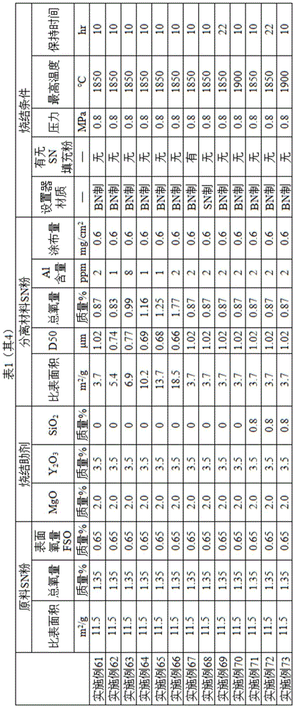
TABLE 5
Table 2 (1)

TABLE 6
Table 2 (its 2)

TABLE 7
Table 2 (its 3)

TABLE 8
Table 2 (4 thereof)

In the above-described embodiment, since SN powder is used as the separating material, BN powder does not remain on the surface of the silicon nitride substrate, and therefore, the heat cycle resistance when copper is bonded to the silicon nitride substrate can be made excellent. And thenRegarding the amount of BN remaining on the surface after removal of the separating material from the surface of the silicon nitride substrate, the ratio (B/Si) of the fluorescent X-ray intensity of boron (B) to the fluorescent X-ray intensity of silicon (Si) is 12X 10- 5 In the following, the number of cases was very small, and not only the heat cycle resistance was excellent when copper was bonded to the silicon nitride substrate, but also BN was not detected on the surface of the silicon nitride substrate when an SN setter or a filler powder of SN powder was used.
As shown in examples 1 to 44 of tables 1 and 2, a specific surface area of 1m was used 2 Above/g and 20m 2 Silicon Nitride (SN) powder having a D50 of 20 μm or less, an oxygen content of 0.3% by mass or more and less than 2% by weight and an aluminum content of less than 50ppm is used as a separating material, and the coating amount of the SN powder on the surface of the green sheet is set to 0.1mg/cm 2 Above 3mg/cm 2 In the following, in all of examples 1 to 44, it was confirmed that the releasability after firing was good, and a silicon nitride substrate having a flexural strength of 900MPa or more, a thermal conductivity of 90W/(m·k) or more, and further 95W/(m·k) or more was obtained.
In example 51, the specific surface area of the separation material SN powder was 0.4m 2 At/g, the releasability after sintering was inferior to that of example 1, and the bending strength was 850MPa.
In example 52, the specific surface area of the separation material SN powder was set to 23.2m 2 At/g, the releasability after sintering was inferior to that of example 1, and the bending strength was 800MPa.
In example 53, when the aluminum content of the SN powder as a separating material was 70ppm, the releasability was good, but the thermal conductivity was 80W/(m·k).
In examples 54 and 55, the coating amounts of the SN powder as a separating material were set to 0.07 and 3.5mg/cm 2 When the releasability after sintering was inferior to that of example 1, the flexural strength was 830 and 800MPa.
In example 56, when the highest temperature at the time of sintering was set to 1900 ℃, the area ratio of columnar crystal particles of the obtained silicon nitride substrate became as high as 43%, and the peeling property after peeling and sintering was inferior to that of example 1, and the bending strength was 780MPa.
In example 57, assuming that the maximum temperature and the holding time at the time of sintering were 30 hours, the area ratio of columnar crystal particles of the obtained silicon nitride substrate became as high as 53%, and the peeling property after sintering was inferior to that of example 1, and the bending strength was 730MPa.
In example 58, when the gas pressure at the time of sintering was set to 4MPa, the area ratio of the obtained silicon nitride substrate became as high as 37%, and the peeling property after sintering was inferior to that of example 1, and the bending strength was 840MPa.
In example 59, the area ratio was 12% and the releasability was good, but the bending strength was 860MPa and the thermal conductivity was 80W/(m·k), assuming that the highest temperature at the time of sintering was 1780 ℃.
In examples 51 to 59, the flexural strength and thermal conductivity of the silicon nitride substrates were inferior to those of examples 1 to 44, but were equal to or higher than those of the substrates based on the prior art, and were excellent. Furthermore, the surface of the silicon nitride substrate was free from BN powder remaining, and although a BN setter was used, the ratio (B/Si) of the fluorescent X-ray intensity of boron (B) to the fluorescent X-ray intensity of silicon (Si) was 16X 10 -5 In the following, a very small number is a substrate that can be made excellent in heat cycle resistance when copper is bonded to a silicon nitride substrate.
In examples 61 to 66, the raw material SN powder had a specific surface area of 11.5m 2 When the total oxygen content per gram is 1.35%, the flexural strength of the silicon nitride substrate is 830 to 880MPa, and the thermal conductivity is 86 to 87W/(mK).
In example 67, the specific surface area of the raw material SN powder was 11.5m 2 When the total oxygen content per gram was 1.35% and the periphery of the green sheet was covered with Silicon Nitride (SN) powder, boron (B) was not detected on the silicon nitride substrate, and the flexural strength of the silicon nitride substrate was 890MPa and the thermal conductivity was 87W/(m·k).
In example 68, the specific surface area of the raw SN powder was 11.5m 2 When the total oxygen content per gram was 1.35% and the Silicon Nitride (SN) setter was used, boron (B) was not detected on the silicon nitride substrate, and the flexural strength of the silicon nitride substrate was 870MPa and the thermal conductivity was 86W/(m·k).
In example 69, the specific surface area of the raw material SN powder was 11.5m 2 The total oxygen content per gram is 1.35%When the holding time at the highest temperature during sintering was 22 hours, the flexural strength of the silicon nitride substrate was 830MPa and the thermal conductivity was 90W/(mK).
In example 70, the specific surface area of the raw material SN powder was set to 11.5m 2 When the total oxygen content per gram was 1.35% and the maximum temperature at the time of sintering was 1900 ℃, the flexural strength of the silicon nitride substrate was 820MPa and the thermal conductivity was 92W/(mK).
In example 71, the specific surface area of the raw material SN powder was 11.5m 2 1.35% of SiO was added to the total oxygen content per gram, and 0.8% by mass of SiO was added to the mixture 2 When the sintering aid was used and the highest temperature at the time of sintering was 1900 ℃, the bending strength of the silicon nitride substrate was 850MPa and the thermal conductivity was 88W/(m·k).
In example 72, the specific surface area of the raw material SN powder was 11.5m 2 1.35% of SiO was added to the total oxygen content per gram, and 0.8% by mass of SiO was added to the mixture 2 When the sintering aid was used and the holding time at the highest temperature at the time of sintering was 22 hours, the flexural strength of the silicon nitride substrate was 830MPa and the thermal conductivity was 93W/(m·k).
In example 73, the specific surface area of the raw material SN powder was 11.5m 2 1.35% of SiO was added to the total oxygen content per gram, and 0.8% by mass of SiO was added to the mixture 2 When the sintering aid was used and the holding time at the highest temperature at the time of sintering was 22 hours, the flexural strength of the silicon nitride substrate was 810MPa and the thermal conductivity was 95W/(m·k).
In examples 61 to 73, the flexural strength and thermal conductivity of the silicon nitride substrates were inferior to those of examples 1 to 44, but were equal to or higher than those of the substrates based on the prior art, and were excellent. Further, even in the case of using a BN setter, by using SN powder as a separating material, the surface of the silicon nitride substrate is free from BN powder remaining, and the ratio (B/Si) of the fluorescent X-ray intensity of boron (B) to the fluorescent X-ray intensity of silicon (Si) of the silicon nitride substrate is 14.5X10 -5 In the following, the amount is very small. When the periphery of the green sheet was covered with SN powder or an SN setter was used, the fluorescent X-ray intensity of boron (B) was not detected on the silicon nitride substrate. Therefore, the silicon nitride substrates of examples 61 to 73 can be used to formThe heat cycle resistance when copper is bonded is excellent.
Industrial applicability
The method for producing a silicon nitride substrate according to the present invention can provide a silicon nitride substrate having excellent heat cycle resistance when copper is bonded, which is obtained by stacking and sintering a plurality of green sheets and then separating the green sheets, and further can provide a silicon nitride substrate having excellent peelability, high flexural strength and high thermal conductivity, and little deformation. The silicon nitride substrate can be used as a substrate for a power element module or the like.
Description of the reference numerals
1. Separating material (SN powder)
2. Green sheet
3. Setting device
4. Spacer(s)
5. Filling powder (SN powder)
8. Silicon nitride particles (columnar crystal particles)
9. Separating material (SN powder)
Claims (14)
1. A method for producing a silicon nitride substrate, characterized in that a plurality of green sheets comprising silicon nitride powder and a sintering aid are stacked with a separator comprising only silicon nitride powder disposed therebetween,
sintering the plurality of green sheets in the obtained laminate,
A plurality of silicon nitride sintered bodies are obtained by separation from the laminated body, and,
a silicon nitride substrate is obtained from the silicon nitride sintered body,
the silicon nitride substrate is a silicon nitride substrate formed from a silicon nitride sintered body containing silicon nitride particles and a sintering aid, wherein the silicon nitride particles have a columnar crystal particle diameter a of 0.5 to 5 [ mu ] m and a ratio b/a of a long diameter b to a short diameter a of 2 or more of less than 30% in terms of an area ratio in the substrate surface, and,
the separation material was used at 0.1mg/cm 2 Above and 3mg/cm 2 The following coating amounts were applied to the aboveThe surface of the green sheet.
2. The method for manufacturing a silicon nitride substrate according to claim 1, wherein the sintering of the plurality of green sheets is performed in a silicon nitride surrounding body or a boron nitride surrounding body.
3. The method for producing a silicon nitride substrate according to claim 1 or 2, wherein the sintering is performed by covering the periphery of the plurality of green sheets with silicon nitride powder.
4. The method for producing a silicon nitride substrate according to claim 1 or 2, wherein the separation material remaining on the surface of the silicon nitride sintered body obtained after the sintering is removed.
5. The method for producing a silicon nitride substrate according to claim 1 or 2, wherein the specific surface area of the separating material measured by a BET method is 1m 2 Above/g and 20m 2 And/g or less, a 50% particle diameter D50 of 20 μm or less on the basis of volume as measured by a laser diffraction scattering method, and an oxygen amount of 0.3 wt% or more and less than 2 wt%.
6. The method of producing a silicon nitride substrate according to claim 5, wherein the aluminum content of the separation material is less than 50ppm.
7. The method according to claim 5, wherein the sintering is performed in a nitrogen atmosphere at a gas pressure of 0.15MPa to 3MPa, a sintering temperature of 1750 ℃ to 1910 ℃ for 6 hours to 22 hours.
8. A silicon nitride substrate obtained by the method according to claim 1, which is a silicon nitride substrate formed of a silicon nitride sintered body containing silicon nitride particles and a sintering aid, wherein the silicon nitride particles are sintered with a sintering aidThe thickness of the silicon nitride substrate is 0.5mm or less, the ratio of boron nitride to silicon nitride in the surface of the substrate is less than 6.5X10 as the ratio B/Si of the fluorescence X-ray intensity of boron B to the fluorescence X-ray intensity of silicon Si -5 。
9. A silicon nitride substrate obtained by the method according to claim 1, wherein the silicon nitride substrate is a silicon nitride substrate formed of a silicon nitride sintered body containing silicon nitride particles and a sintering aid, and columnar crystal particles having a short diameter a of 0.5 to 5 μm and a ratio B/a of long diameter B to short diameter a of 2 or more are set to less than 30% in terms of an area ratio in the substrate surface, and the arithmetic average surface roughness of the substrate surface is 0.03 μm or more and 0.5 μm or less, and the ratio of boron nitride to silicon nitride in the substrate surface is set to less than 6.5X10 in terms of a ratio B/Si of fluorescent X-ray intensity of boron B to fluorescent X-ray intensity of silicon Si -5 。
10. The silicon nitride substrate of claim 9 wherein the surface of the substrate is free of boron nitride powder.
11. The silicon nitride substrate according to claim 9 or 10, wherein the thermal conductivity is 80W/(mj/K) or more at room temperature and the 4-point bending strength is 800MPa or more at room temperature.
12. A silicon nitride substrate according to claim 9 or 10, wherein the aluminium content of the separation material is less than 50ppm.
13. The silicon nitride substrate according to claim 9 or 10, wherein the thickness is 0.5mm or less.
14. An insulating substrate or a circuit board, wherein the silicon nitride substrate according to any one of claims 8 to 13 is used.
Applications Claiming Priority (3)
| Application Number | Priority Date | Filing Date | Title |
|---|---|---|---|
| JP2018-206946 | 2018-11-01 | ||
| JP2018206946 | 2018-11-01 | ||
| PCT/JP2019/042413 WO2020090832A1 (en) | 2018-11-01 | 2019-10-29 | Silicon nitride substrate production method and silicon nitride substrate |
Publications (2)
| Publication Number | Publication Date |
|---|---|
| CN112912356A CN112912356A (en) | 2021-06-04 |
| CN112912356B true CN112912356B (en) | 2023-05-02 |
Family
ID=70463227
Family Applications (1)
| Application Number | Title | Priority Date | Filing Date |
|---|---|---|---|
| CN201980070845.9A Active CN112912356B (en) | 2018-11-01 | 2019-10-29 | Method for manufacturing silicon nitride substrate and silicon nitride substrate |
Country Status (3)
| Country | Link |
|---|---|
| JP (1) | JP7272370B2 (en) |
| CN (1) | CN112912356B (en) |
| WO (1) | WO2020090832A1 (en) |
Families Citing this family (1)
| Publication number | Priority date | Publication date | Assignee | Title |
|---|---|---|---|---|
| CN116161970A (en) * | 2022-12-29 | 2023-05-26 | 无锡海古德新技术有限公司 | Lamination sintering process method of high-performance silicon nitride ceramic substrate |
Citations (6)
| Publication number | Priority date | Publication date | Assignee | Title |
|---|---|---|---|---|
| JPH1086279A (en) * | 1996-09-18 | 1998-04-07 | Toshiba Corp | Silicon nitride multilayered substrate and its production |
| JP2000072552A (en) * | 1998-08-31 | 2000-03-07 | Kyocera Corp | Silicon nitride heat radiation member and its production |
| JP2001019557A (en) * | 1999-06-30 | 2001-01-23 | Denki Kagaku Kogyo Kk | Silicon nitride sintered compact, its production and substrate |
| JP2002293642A (en) * | 2001-03-30 | 2002-10-09 | Hitachi Metals Ltd | Silicon nitride-based sintered compact having high thermal conductivity, method of producing the same, and circuit board |
| WO2013121861A1 (en) * | 2012-02-13 | 2013-08-22 | 三井金属鉱業株式会社 | Silicon nitride sintered body and method for producing same |
| CN106470939A (en) * | 2014-06-16 | 2017-03-01 | 宇部兴产株式会社 | Alpha-silicon nitride powders, silicon nitride sinter and circuit substrate and the manufacture method of alpha-silicon nitride powders |
Family Cites Families (13)
| Publication number | Priority date | Publication date | Assignee | Title |
|---|---|---|---|---|
| JPH02246105A (en) * | 1989-03-17 | 1990-10-01 | Sumitomo Metal Ind Ltd | Manufacture of ceramic element assembly |
| US5759933A (en) * | 1991-04-09 | 1998-06-02 | Alliedsignal Inc. | Gas pressure sintered silicon nitride having high strength and stress rupture resistance |
| EP0589997B1 (en) * | 1991-06-17 | 1995-07-19 | AlliedSignal Inc. | High toughness-high strength sintered silicon nitride |
| JP3981482B2 (en) * | 1998-12-25 | 2007-09-26 | 日本特殊陶業株式会社 | Method for producing silicon nitride sintered body and method for producing ceramic heater |
| JP2010208898A (en) * | 2009-03-11 | 2010-09-24 | Hitachi Metals Ltd | Silicon nitride substrate, method for producing the same and circuit board using the same |
| JP5339214B2 (en) * | 2010-03-01 | 2013-11-13 | 日立金属株式会社 | Method for manufacturing silicon nitride substrate and silicon nitride substrate |
| JP5440947B2 (en) * | 2010-03-31 | 2014-03-12 | 日立金属株式会社 | Silicon nitride substrate manufacturing method, silicon nitride substrate, and circuit board using the same |
| JP5743752B2 (en) * | 2011-06-29 | 2015-07-01 | 京セラ株式会社 | Circuit board |
| US9655237B2 (en) * | 2011-10-11 | 2017-05-16 | Hitachi Metals, Ltd. | Silicon nitride substrate and method for producing silicon nitride substrate |
| JP5729519B2 (en) * | 2012-03-26 | 2015-06-03 | 日立金属株式会社 | Sintered silicon nitride substrate and manufacturing method thereof |
| JP5975176B2 (en) * | 2013-07-11 | 2016-08-23 | 宇部興産株式会社 | Silicon nitride powder for mold release agent of polycrystalline silicon ingot casting mold and manufacturing method thereof, slurry containing silicon nitride powder, casting mold for polycrystalline silicon ingot and manufacturing method thereof, and polycrystalline silicon using the mold Manufacturing method of ingot casting |
| US10308560B2 (en) * | 2015-01-23 | 2019-06-04 | Kabushiki Kaisha Toshiba | High thermal conductive silicon nitride sintered body, and silicon nitride substrate and silicon nitride circuit board and semiconductor apparatus using the same |
| CN106631039A (en) * | 2016-11-04 | 2017-05-10 | 广东工业大学 | Preparation method of silicon nitride ceramic substrate |
-
2019
- 2019-10-29 CN CN201980070845.9A patent/CN112912356B/en active Active
- 2019-10-29 JP JP2020553947A patent/JP7272370B2/en active Active
- 2019-10-29 WO PCT/JP2019/042413 patent/WO2020090832A1/en active Application Filing
Patent Citations (6)
| Publication number | Priority date | Publication date | Assignee | Title |
|---|---|---|---|---|
| JPH1086279A (en) * | 1996-09-18 | 1998-04-07 | Toshiba Corp | Silicon nitride multilayered substrate and its production |
| JP2000072552A (en) * | 1998-08-31 | 2000-03-07 | Kyocera Corp | Silicon nitride heat radiation member and its production |
| JP2001019557A (en) * | 1999-06-30 | 2001-01-23 | Denki Kagaku Kogyo Kk | Silicon nitride sintered compact, its production and substrate |
| JP2002293642A (en) * | 2001-03-30 | 2002-10-09 | Hitachi Metals Ltd | Silicon nitride-based sintered compact having high thermal conductivity, method of producing the same, and circuit board |
| WO2013121861A1 (en) * | 2012-02-13 | 2013-08-22 | 三井金属鉱業株式会社 | Silicon nitride sintered body and method for producing same |
| CN106470939A (en) * | 2014-06-16 | 2017-03-01 | 宇部兴产株式会社 | Alpha-silicon nitride powders, silicon nitride sinter and circuit substrate and the manufacture method of alpha-silicon nitride powders |
Also Published As
| Publication number | Publication date |
|---|---|
| JP7272370B2 (en) | 2023-05-12 |
| JPWO2020090832A1 (en) | 2021-09-16 |
| CN112912356A (en) | 2021-06-04 |
| WO2020090832A1 (en) | 2020-05-07 |
Similar Documents
| Publication | Publication Date | Title |
|---|---|---|
| EP2767524B1 (en) | Silicon nitride substrate and method for manufacturing silicon nitride substrate | |
| JP5339214B2 (en) | Method for manufacturing silicon nitride substrate and silicon nitride substrate | |
| WO2014080536A1 (en) | Metal-ceramic bonded substrate and method for producing same | |
| KR101751531B1 (en) | Method for producing silicon nitride substrate | |
| JP7062229B2 (en) | Plate-shaped silicon nitride sintered body and its manufacturing method | |
| JP2007059178A (en) | Heater unit and device equipped with it | |
| JP5440947B2 (en) | Silicon nitride substrate manufacturing method, silicon nitride substrate, and circuit board using the same | |
| WO2022196693A1 (en) | Silicon nitride substrate | |
| CN112912356B (en) | Method for manufacturing silicon nitride substrate and silicon nitride substrate | |
| KR20230049628A (en) | Laminates for circuit boards | |
| CN116134608A (en) | Silicon nitride substrate and method for manufacturing same | |
| TW202208308A (en) | Silicon nitride sintered substrate | |
| JP4596855B2 (en) | Metal-ceramic composite structure and electrode member for plasma generation comprising the same | |
| JP2022159414A (en) | silicon nitride substrate | |
| CN114787105B (en) | Plate-like silicon nitride sintered body and method for producing same | |
| JP5073135B2 (en) | Aluminum nitride sintered body, production method and use thereof | |
| JP4347206B2 (en) | Manufacturing method of ceramic sheet, ceramic substrate using the same, and use thereof | |
| WO2018021491A1 (en) | Ceramic joined body | |
| JP7339980B2 (en) | Manufacturing method of silicon nitride sintered body | |
| JP7339979B2 (en) | Manufacturing method of silicon nitride sintered body | |
| JP7432040B2 (en) | silicon nitride sintered body | |
| JP7201734B2 (en) | Silicon nitride sintered body | |
| JP7278326B2 (en) | Manufacturing method of silicon nitride sintered body | |
| WO2024084631A1 (en) | Silicon nitride sintered body | |
| KR102139189B1 (en) | Memufacturing method of conductivity AlN subtrate having thermal conductivity of 180 W/mk to 230 W/mk |
Legal Events
| Date | Code | Title | Description |
|---|---|---|---|
| PB01 | Publication | ||
| PB01 | Publication | ||
| SE01 | Entry into force of request for substantive examination | ||
| SE01 | Entry into force of request for substantive examination | ||
| CB02 | Change of applicant information |
Address after: Yamaguchi Japan Applicant after: Ube Co.,Ltd. Address before: Yamaguchi Japan Applicant before: UBE INDUSTRIES, Ltd. |
|
| CB02 | Change of applicant information | ||
| GR01 | Patent grant | ||
| GR01 | Patent grant |