CN1127204C - Planar resist structure esp encapsulation for electric components and thermomechanical method for prodn thereof - Google Patents
Planar resist structure esp encapsulation for electric components and thermomechanical method for prodn thereof Download PDFInfo
- Publication number
- CN1127204C CN1127204C CN99807714A CN99807714A CN1127204C CN 1127204 C CN1127204 C CN 1127204C CN 99807714 A CN99807714 A CN 99807714A CN 99807714 A CN99807714 A CN 99807714A CN 1127204 C CN1127204 C CN 1127204C
- Authority
- CN
- China
- Prior art keywords
- photosensitive layer
- etchant resist
- layer
- carrier
- diaphragm
- Prior art date
- Legal status (The legal status is an assumption and is not a legal conclusion. Google has not performed a legal analysis and makes no representation as to the accuracy of the status listed.)
- Expired - Lifetime
Links
Images


Classifications
-
- H—ELECTRICITY
- H03—ELECTRONIC CIRCUITRY
- H03H—IMPEDANCE NETWORKS, e.g. RESONANT CIRCUITS; RESONATORS
- H03H9/00—Networks comprising electromechanical or electro-acoustic devices; Electromechanical resonators
- H03H9/02—Details
- H03H9/05—Holders; Supports
- H03H9/10—Mounting in enclosures
- H03H9/1064—Mounting in enclosures for surface acoustic wave [SAW] devices
-
- H—ELECTRICITY
- H03—ELECTRONIC CIRCUITRY
- H03H—IMPEDANCE NETWORKS, e.g. RESONANT CIRCUITS; RESONATORS
- H03H3/00—Apparatus or processes specially adapted for the manufacture of impedance networks, resonating circuits, resonators
- H03H3/007—Apparatus or processes specially adapted for the manufacture of impedance networks, resonating circuits, resonators for the manufacture of electromechanical resonators or networks
- H03H3/08—Apparatus or processes specially adapted for the manufacture of impedance networks, resonating circuits, resonators for the manufacture of electromechanical resonators or networks for the manufacture of resonators or networks using surface acoustic waves
-
- H—ELECTRICITY
- H03—ELECTRONIC CIRCUITRY
- H03H—IMPEDANCE NETWORKS, e.g. RESONANT CIRCUITS; RESONATORS
- H03H9/00—Networks comprising electromechanical or electro-acoustic devices; Electromechanical resonators
- H03H9/02—Details
- H03H9/05—Holders; Supports
-
- H—ELECTRICITY
- H03—ELECTRONIC CIRCUITRY
- H03H—IMPEDANCE NETWORKS, e.g. RESONANT CIRCUITS; RESONATORS
- H03H9/00—Networks comprising electromechanical or electro-acoustic devices; Electromechanical resonators
- H03H9/02—Details
- H03H9/05—Holders; Supports
- H03H9/10—Mounting in enclosures
- H03H9/1064—Mounting in enclosures for surface acoustic wave [SAW] devices
- H03H9/1071—Mounting in enclosures for surface acoustic wave [SAW] devices the enclosure being defined by a frame built on a substrate and a cap, the frame having no mechanical contact with the SAW device
Abstract
According to the inventive thermomechanical method for planing a resist layer which is applied on a partially raised supporting surface, a resist structure, especially an encapsulation for electronic components, is obtained. To this end, a dry resist film (2) which is comprised of a composite made of a temperature resistant protective film (3) and of a photosensitive layer (4) is applied with the photosensitive layer (4) thereof on the supporting surface (6). The dry resist film (2d) is planed using pressure and heat, whereupon the photosensitive layer is exposed. Afterwards, the protective film (3) is removed and the photosensitive layer is developed.
Description
Technical field
The present invention relates to a kind of plane structure against corrosion, in particular for the packed part of electronic component and be used to make the thermomechanical method that is applied to the structure sheaf complanation on the bearing-surface that part raises.
Background technology
By international publication number be the PCT application of WO95/30276 known a kind of be used for electronic component-especially with the element (OFW element) of surface acoustic wave work, the defending party to the application is called the encapsulation of PROTEC, this element is in the component structure zone, promptly for example have a groove that receives it in sandwich digit transducer (Interdigital-wandler) zone and in the SATT body region that must apply usually in case of necessity in screen printing technique.For this reason, described this PCT application is provided with the shaped as frame carrier that is applied on component substrate such as the Piezoelectric Substrates and reaches in case of necessity supporting in an one embodiment, cover layer is set thereon.In the case, this carrier, supporting and cover layer can be made of a film, and it comprises the depression of overstress on the component substrate side, and by for example bonding, welding or stacked being applied on the component substrate.
According to another known suggestion of this PCT application, can use a kind of material that constitutes by camera technique, so-called dried etchant resist for example for this carrier and supporting in case of necessity.This for example can be a kind of photoresist or a kind ofly form the material of structure by UV (ultraviolet) light, and it is exposed in this wise, promptly only exposes active element, especially filter structure, SATT body and electrically contact the face of setting for this element after it develops.In the carrier that makes like this and (if any) supporting, apply the second layer then, i.e. cover layer, it also is by a dried etchant resist, is the material that camera technique constitutes that passes through of the above-mentioned type that it is exposed equally and develops after coating.This material constitutes depression under the adequate thickness situation that the ground floor of being made up of carrier and supporting in case of necessity and this material form together at last.
This encapsulation that is also referred to as PROTEC, promptly at last by two-layer stack each other and respectively all situations of the box-like by the coat composed encapsulation of the dried etchant resist of camera technique respective handling-consideration ground floor or shaped as frame structure-need directly be placed on the SATT body for dried etchant resist therein be inapplicable.
The ground floor that is applied in or the first dried etchant resist and the second layer or the second dried etchant resist will be followed the uneven height profile of SATT body when conventional coating thus.Yet it is unacceptable applying the second dried etchant resist unevenly on the uneven first dried etchant resist that applies, because the encapsulation that is produced under the technical rational coating condition of the second layer, the covering that for example is used for the chip of OFW element will be packing less completely.
Summary of the invention
Task of the present invention is, provides a kind of element and manufacture method thereof with structure against corrosion, and they can guarantee reliably applying of the second layer or dried etchant resist and guarantee electronic component chip, the especially level Hermetic Package of OFW element thus.
This task will solve by following, promptly propose a kind of electronic component: have and be applied to a rising structure on the carrier; Have one and be applied to the structural structure against corrosion that raises; Structure wherein against corrosion is placed on carrier and the rising structure hermetically, reaches the layer thickness that structure wherein against corrosion has such variation, and structure promptly against corrosion is not flat with the surface that carrier and rising structure contact.Plane at first according to the present invention structure against corrosion can realize evenly applying of another layer, combines well with structure against corrosion with activation, adheres to reliably to reach the encapsulation that the result can produce sealing on it.
Structure wherein against corrosion is covered by the resist layer of another uniform layer thickness.
Structure wherein against corrosion constitutes a frame, and another resist layer constitutes the lid that is fit to this frame, and frame and lid form the covering of a cap shape together, and surrounds a hollow space between carrier, frame and lid.
Structure against corrosion and another resist layer are made of dried etchant resist.
The present invention also proposes to be used for making the thermomechanical method of plane structure against corrosion on a carrier surface, carrier surface has raised portion, be used for the encapsulation of electronic component, if wherein with the diaphragm of a dried etchant resist of the combined formation of photosensitive layer be a heatproof, promptly at high temperature can ruined film, as solution, the method according to this invention is provided with thus: dried etchant resist is placed on the carrier side with its photosensitive layer; Dried etchant resist is handled under pressure and heat like this, and promptly its photosensitive layer is formed the plane; And make the photosensitive layer exposure, then remove diaphragm and photosensitive layer is developed.
If use a kind of diaphragm of non-heatproof, then the present invention is provided with: remove diaphragm and replace it by a heatproof barrier film from photosensitive layer after applying dried etchant resist, this heatproof barrier film is having an antistick layer on the surface of photosensitive layer; Barrier film and photosensitive layer are handled under pressure and heat like this, and promptly its photosensitive layer is formed the plane; Barrier film is removed and is then made photosensitive layer exposure and development.
For the dried etchant resist of ground floor apply or coating be carry out according to the conventional criteria method and produced a bubble-free layer, it has followed for example the geometric profile of the decay body that applies with screen printing technique.Just by complanation, promptly wherein be placed between the hot plate and compress being placed on dried etchant resist and carrier between the hot plate under the situation of heatproof diaphragm and compressing and under the situation of non-heatproof diaphragm, will be coated with the carrier of photosensitive layer and barrier film; because the rising of temperature makes the viscosity of the photosensitive material of ground floor be reduced to such degree, promptly the material that makes this layer by the pressure that acts on carrier in the axial direction is from being positioned at zone flows in the silk screen printing to the zone of undamped body.
Therefore, the photosensitive layer of ground floor is leveled to such degree, and promptly forming the back second layer dried etchant resist in the structure of following against corrosion can be with known mode coating itself and the encapsulation that is produced, can be sealed airtightly as the chip of electronic component.
The adhesion of material on hot plate will be avoided by diaphragm, the intrinsic enough heat resistances of for example polyester film.
It is the present invention also proposes to be used for making plane structure against corrosion on a carrier surface thermomechanical method; carrier surface has raised portion; be used for the encapsulation of electronic component; wherein by a dried etchant resist that constitutes of heatproof diaphragm and photosensitive layer, be placed on the carrier side with photosensitive layer, wherein dried etchant resist is handled under pressure and heat like this; the photosensitive layer that is it is flattened; and wherein make the photosensitive layer exposure, and then remove diaphragm and photosensitive layer is developed, obtain structure against corrosion thus.
The present invention also proposes to be used for making the thermomechanical method of plane structure against corrosion on a carrier surface, carrier surface has raised portion, is used for the encapsulation of electronic component; By the dried etchant resist that constitutes of heatproof diaphragm and photosensitive layer not, be placed on the carrier side with photosensitive layer; After applying dried etchant resist, to remove the not diaphragm of heatproof from photosensitive layer, and replace by a heatproof barrier film, this heatproof barrier film is having an antistick layer on the surface of photosensitive layer; Heatproof barrier film and photosensitive layer are handled under pressure and heat like this, and promptly its photosensitive layer is flattened; The heatproof barrier film is removed, and then made photosensitive layer exposure and development, obtain structure against corrosion thus.
On the photosensitive layer that has developed, apply the second dried etchant resist that constitutes by diaphragm and photosensitive layer; photosensitive layer with the second dried etchant resist is applied on the photosensitive layer that has developed; then make the photosensitive layer exposure of the second dried etchant resist, remove the diaphragm of the second dried etchant resist then and the photosensitive layer of the second dried etchant resist is developed.
Wherein on the photosensitive layer that has developed, apply the second dried etchant resist that constitutes by diaphragm and photosensitive layer; photosensitive layer with the second dried etchant resist is placed on the photosensitive layer that has developed; then remove the diaphragm of the second dried etchant resist, expose then and develop.
This photosensitive layer that has developed is solidified.
Wherein make dried etchant resist and carrier be placed between the hot plate and compress.
Wherein make and carrier that photosensitive layer stacks and barrier film are placed between the hot plate and compress.
Wherein use diaphragm or the barrier film of a kind of polyester film as heatproof.
Wherein use the not diaphragm of heatproof of polyolefin film conduct.
Antistick layer is silicon layer or polytetrafluoroethylene floor.
Above method is used to make the surface acoustic wave component that has as the wafer of carrier.
Below will at length explain the present invention by the embodiment of expression in the accompanying drawings.Accompanying drawing is:
Description of drawings
Fig. 1 to 3 is perspective cross-sectional slice of the main method step of first embodiment according to the inventive subject matter;
Fig. 4 to 7 is diagrammatic sketch that are similar to Fig. 1 to 3 of main method step according to a second embodiment of the present invention.
Embodiment
Identical in the accompanying drawings part is represented with identical label.
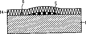
In described first embodiment, express the manufacturing (seeing Fig. 1 to 3) of an OFW element, on the surface 6 of a carrier 1 of doing by piezoelectric, promptly in extensive usually the manufacturing, have in the zone of each OFW element therein that the mode with routine applies the dried etchant resist 2 of one deck on the wafer of SATT body 5 of the rising structure that applies with screen printing technique for example.This dried etchant resist 2 itself is by a heatproof diaphragm 3, as the (see figure 1) that constitutes of a polyester film and a photosensitive layer 4.
(see figure 2) in another step, the wafer of such coating is placed on the hot plate 7 of a pressure apparatus, between 8 and make dried etchant resist 2 under pressure (seeing arrow F) and heat, form the plane (see figure 3), wherein see that from direction of arrow A this photosensitive material partly flows to the zone of undamped body.
Then, make photosensitive layer 4 exposures, remove diaphragm 3 and the photosensitive layer 4 of exposure is developed, finished the manufacturing step of a PROTEC layer thus.
Also use the dried etchant resist of above-mentioned characteristic as the 2nd required PROTEC layer of finished product that forms complete encapsulation; it is applied on the plane layer 4 that has developed in known manner together with its photosensitive layer; make its photosensitive layer exposure then, remove its diaphragm and the photosensitive layer of exposure is developed.
Example can replace the above-mentioned dried etchant resist that is used to have the 2nd PROTEC layer of its heatproof diaphragm as an alternative, on the layer 4 that has developed, apply one have heatproof diaphragm not, as the dried etchant resist of polyolefin film.May to after removing diaphragm, just carry out the exposure of photosensitive layer because employed wavelength is not had enough transmissivities in this case.
For last encapsulation, after applying and develop, second photosensitive layer make this layer that has developed by for example ultraviolet (UV) ray and/or heating are cured.
In method according to the embodiment of Fig. 4 to 7, used a kind of dried etchant resist 12 for a PROTEC layer, it is by a non-heatproof diaphragm 13, as the (see figure 4) that constitutes of a polyolefin film and a photosensitive layer 14.Because it does not have this diaphragm of enough heat resistances to be removed (see figure 5) in the past in described complanation just now, and is replaced by heatproof barrier film 15, for example polyester film.This barrier film has for example a silicon layer or a polytetrafluoroethylene floor (PTFE layer) 17 at it on the surface of carrier 1, (see figure 6) can avoid photosensitive layer 14 to be bonded on the hot plate 7 when the complanation of following, and can remove barrier film 15 from photosensitive layer 14 subsequently.
After finishing complanation (as described for first embodiment just now) will remove barrier film 15 and then make photosensitive layer 14 exposures and develop, form a PROTEC layer of encapsulation thus.
To make in one of mode described in first embodiment according to employed film for the 2nd PROTEC layer, therefore not need to redescribe again these making steps.
Claims (15)
1. electronic component,
-have and be applied to a rising structure on the carrier,
-have one to be applied to the structural structure against corrosion that raises,
-structure wherein against corrosion is placed on carrier and the rising structure hermetically, and
-structure wherein against corrosion has the layer thickness of such variation, and structure promptly against corrosion is not flat with the surface that carrier and rising structure contact.
2. according to the element of claim 1, structure wherein against corrosion is covered by the resist layer of another uniform layer thickness.
3. according to the element of claim 2,
-structure wherein against corrosion constitutes a frame,
-wherein another resist layer constitutes the lid that is fit to this frame,
-its center and lid form the covering of a cap shape together, and surround a hollow space between carrier, frame and lid.
4. according to one element in the claim 2 to 3, structure wherein against corrosion and another resist layer are made of dried etchant resist.
5. be used for making on a carrier surface thermomechanical method of plane structure against corrosion, carrier surface has raised portion, is used for the encapsulation of electronic component,
Dried etchant resist that constitutes by heatproof diaphragm and photosensitive layer is placed on the carrier side with photosensitive layer,
Wherein dried etchant resist is handled under pressure and heat like this, and promptly its photosensitive layer is flattened, and
Wherein make the photosensitive layer exposure, then remove diaphragm and photosensitive layer is developed, obtain structure against corrosion thus.
6. be used for making on a carrier surface thermomechanical method of plane structure against corrosion, carrier surface has raised portion, is used for the encapsulation of electronic component,
By the dried etchant resist that constitutes of heatproof diaphragm and photosensitive layer not, be placed on the carrier side with photosensitive layer,
After applying dried etchant resist, to remove the not diaphragm of heatproof from photosensitive layer, and replace by a heatproof barrier film, this heatproof barrier film is having an antistick layer on the surface of photosensitive layer;
Heatproof barrier film and photosensitive layer are handled under pressure and heat like this, and promptly its photosensitive layer is flattened;
The heatproof barrier film is removed, and then made photosensitive layer exposure and development, obtain structure against corrosion thus.
7. according to the method for claim 5 or 6; wherein on the photosensitive layer that has developed, apply the second dried etchant resist that constitutes by diaphragm and photosensitive layer; photosensitive layer with the second dried etchant resist is applied on the photosensitive layer that has developed; then make the photosensitive layer exposure of the second dried etchant resist, remove the diaphragm of the second dried etchant resist then and the photosensitive layer of the second dried etchant resist is developed.
8. according to the method for claim 5 or 6; wherein on the photosensitive layer that has developed, apply the second dried etchant resist that constitutes by diaphragm and photosensitive layer; photosensitive layer with the second dried etchant resist is placed on the photosensitive layer that has developed; then remove the diaphragm of the second dried etchant resist, expose then and develop.
9. according to the method for claim 5 or 6, wherein after the photosensitive layer of the second dried etchant resist applies and develops, this photosensitive layer that has developed is solidified.
10. according to the method for claim 5, wherein make dried etchant resist and carrier be placed between the hot plate and compress.
11., wherein make and carrier that photosensitive layer stacks and barrier film are placed between the hot plate and compress according to the method for claim 6.
12., wherein use diaphragm or the barrier film of a kind of polyester film as heatproof according to the method for claim 5 or 6.
13., wherein use the not diaphragm of heatproof of polyolefin film conduct according to the method for claim 6.
14. according to the method for claim 6, antistick layer is silicon layer or polytetrafluoroethylene floor.
15. according to the method for claim 5 or 6, this method is used to make the surface acoustic wave component that has as the wafer of carrier.
Applications Claiming Priority (2)
| Application Number | Priority Date | Filing Date | Title |
|---|---|---|---|
| DE19820049.8 | 1998-05-05 | ||
| DE19820049A DE19820049C2 (en) | 1998-05-05 | 1998-05-05 | Thermomechanical method for the planarization of a layer that can be structured using photo technology, in particular encapsulation for electronic components |
Publications (2)
| Publication Number | Publication Date |
|---|---|
| CN1306692A CN1306692A (en) | 2001-08-01 |
| CN1127204C true CN1127204C (en) | 2003-11-05 |
Family
ID=7866737
Family Applications (1)
| Application Number | Title | Priority Date | Filing Date |
|---|---|---|---|
| CN99807714A Expired - Lifetime CN1127204C (en) | 1998-05-05 | 1999-05-05 | Planar resist structure esp encapsulation for electric components and thermomechanical method for prodn thereof |
Country Status (8)
| Country | Link |
|---|---|
| US (2) | US6462272B1 (en) |
| EP (1) | EP1078454B1 (en) |
| JP (1) | JP2002513960A (en) |
| KR (1) | KR100651318B1 (en) |
| CN (1) | CN1127204C (en) |
| CA (1) | CA2331277A1 (en) |
| DE (2) | DE19820049C2 (en) |
| WO (1) | WO1999057807A1 (en) |
Families Citing this family (2)
| Publication number | Priority date | Publication date | Assignee | Title |
|---|---|---|---|---|
| CN105870489B (en) * | 2016-06-07 | 2019-03-01 | 程建聪 | Monomer-polymer lithium ion battery manufacturing method and its assemble method |
| US11277689B2 (en) | 2020-02-24 | 2022-03-15 | Logitech Europe S.A. | Apparatus and method for optimizing sound quality of a generated audible signal |
Citations (3)
| Publication number | Priority date | Publication date | Assignee | Title |
|---|---|---|---|---|
| US5410789A (en) * | 1992-11-13 | 1995-05-02 | Murata Manufacturing Co., Ltd. | Method of manufacturing piezoelectric-resonator having vibrating spaces formed therein |
| CN1117666A (en) * | 1994-03-10 | 1996-02-28 | 株式会社村田制作所 | Electronic components and method of manufacturing same |
| DE19548061A1 (en) * | 1995-12-21 | 1997-07-03 | Siemens Matsushita Components | Surface acoustic wave filter |
Family Cites Families (5)
| Publication number | Priority date | Publication date | Assignee | Title |
|---|---|---|---|---|
| US4992354A (en) * | 1988-02-26 | 1991-02-12 | Morton International, Inc. | Dry film photoresist for forming a conformable mask and method of application to a printed circuit board or the like |
| JP3222220B2 (en) * | 1992-10-19 | 2001-10-22 | 株式会社村田製作所 | Manufacturing method of chip type piezoelectric resonator |
| US6420819B1 (en) * | 1994-01-27 | 2002-07-16 | Active Control Experts, Inc. | Packaged strain actuator |
| FI952093A0 (en) * | 1994-05-02 | 1995-05-02 | Siemens Matsushita Components | Kapsling Foer med aciskaiska ytvaogefunktionerande byggelement |
| WO1996004713A1 (en) * | 1994-08-05 | 1996-02-15 | Japan Energy Corporation | Surface acoustic wave device and production method thereof |
-
1998
- 1998-05-05 DE DE19820049A patent/DE19820049C2/en not_active Expired - Fee Related
-
1999
- 1999-05-05 CA CA002331277A patent/CA2331277A1/en not_active Abandoned
- 1999-05-05 DE DE59904049T patent/DE59904049D1/en not_active Expired - Lifetime
- 1999-05-05 EP EP99932628A patent/EP1078454B1/en not_active Expired - Lifetime
- 1999-05-05 WO PCT/DE1999/001352 patent/WO1999057807A1/en active IP Right Grant
- 1999-05-05 JP JP2000547695A patent/JP2002513960A/en not_active Withdrawn
- 1999-05-05 CN CN99807714A patent/CN1127204C/en not_active Expired - Lifetime
- 1999-05-05 KR KR1020007012240A patent/KR100651318B1/en not_active IP Right Cessation
-
2000
- 2000-11-06 US US09/707,029 patent/US6462272B1/en not_active Expired - Lifetime
-
2002
- 2002-07-25 US US10/205,210 patent/US20030000724A1/en not_active Abandoned
Patent Citations (3)
| Publication number | Priority date | Publication date | Assignee | Title |
|---|---|---|---|---|
| US5410789A (en) * | 1992-11-13 | 1995-05-02 | Murata Manufacturing Co., Ltd. | Method of manufacturing piezoelectric-resonator having vibrating spaces formed therein |
| CN1117666A (en) * | 1994-03-10 | 1996-02-28 | 株式会社村田制作所 | Electronic components and method of manufacturing same |
| DE19548061A1 (en) * | 1995-12-21 | 1997-07-03 | Siemens Matsushita Components | Surface acoustic wave filter |
Also Published As
| Publication number | Publication date |
|---|---|
| US20030000724A1 (en) | 2003-01-02 |
| KR100651318B1 (en) | 2006-11-28 |
| CN1306692A (en) | 2001-08-01 |
| WO1999057807A1 (en) | 1999-11-11 |
| DE19820049A1 (en) | 1999-11-25 |
| JP2002513960A (en) | 2002-05-14 |
| US6462272B1 (en) | 2002-10-08 |
| KR20010043280A (en) | 2001-05-25 |
| CA2331277A1 (en) | 1999-11-11 |
| EP1078454A1 (en) | 2001-02-28 |
| DE19820049C2 (en) | 2001-04-12 |
| DE59904049D1 (en) | 2003-02-20 |
| EP1078454B1 (en) | 2003-01-15 |
Similar Documents
| Publication | Publication Date | Title |
|---|---|---|
| US6722030B1 (en) | Process for manufacturing an electronic component, in particular a surface-wave component working with acoustic surface waves | |
| CN1099158C (en) | Encapsulation for electronic components | |
| US7037756B1 (en) | Stacked microelectronic devices and methods of fabricating same | |
| CN100380616C (en) | Electronic device with empty chamby and its producing method | |
| JPH08171339A (en) | Multiple-layer photopolymer hologram laminated body | |
| JP4334139B2 (en) | Diaphragm for capacitive vacuum measuring cell | |
| JPH02134805A (en) | Film capacitor and manufacture of the same | |
| KR20010114238A (en) | Vacuum deposition and curing of oligomers and resins | |
| US4929295A (en) | Method of manufacturing ceramic laminate | |
| CN1205660C (en) | Encapsulation for an electrical component and method for producing the same | |
| CN1127204C (en) | Planar resist structure esp encapsulation for electric components and thermomechanical method for prodn thereof | |
| US6686015B2 (en) | Transferable resilient element for packaging of a semiconductor chip and method therefor | |
| CN1755927A (en) | Semiconductor device and method of manufacturing semiconductor device | |
| JPH10332635A (en) | Sensor element for electrochemical measuring sensor and its manufacture | |
| JP3209304B2 (en) | Laminated electronic component and method of manufacturing the same | |
| JPH0425142A (en) | Manufacture of bonded material and connection of electronic component | |
| WO2001029852A1 (en) | Laminated body manufacturing method and laminated body pressurizing device | |
| WO2019065417A1 (en) | Elastomeric piezoelectric element and elastomeric piezoelectric element production method | |
| JP2003258332A (en) | Manufacturing method for ceramic laminate | |
| JP2950008B2 (en) | Manufacturing method of multilayer ceramic electronic component | |
| JPH05191191A (en) | Manufacture of chip type piezoelectric component | |
| JPS6115584B2 (en) | ||
| JP3802280B2 (en) | Manufacturing method of optical transmitter array original plate | |
| JPH0477205A (en) | Method for compression bonding of ceramic laminate | |
| JPH11261227A (en) | Multilayered circuit board, its manufacture, and modifier |
Legal Events
| Date | Code | Title | Description |
|---|---|---|---|
| C06 | Publication | ||
| PB01 | Publication | ||
| C10 | Entry into substantive examination | ||
| SE01 | Entry into force of request for substantive examination | ||
| C14 | Grant of patent or utility model | ||
| GR01 | Patent grant | ||
| TR01 | Transfer of patent right |
Effective date of registration: 20170912 Address after: American California Patentee after: Snaptrack, Inc. Address before: Munich, Germany Patentee before: Epcos Co., Ltd. |
|
| TR01 | Transfer of patent right | ||
| CX01 | Expiry of patent term |
Granted publication date: 20031105 |
|
| CX01 | Expiry of patent term |