CN112687308A - Low-power consumption static random access memory unit and memory - Google Patents
Low-power consumption static random access memory unit and memory Download PDFInfo
- Publication number
- CN112687308A CN112687308A CN202011595333.5A CN202011595333A CN112687308A CN 112687308 A CN112687308 A CN 112687308A CN 202011595333 A CN202011595333 A CN 202011595333A CN 112687308 A CN112687308 A CN 112687308A
- Authority
- CN
- China
- Prior art keywords
- type transistor
- transistor
- back gate
- random access
- static random
- Prior art date
- Legal status (The legal status is an assumption and is not a legal conclusion. Google has not performed a legal analysis and makes no representation as to the accuracy of the status listed.)
- Pending
Links
- 230000003068 static effect Effects 0.000 title claims abstract description 16
- 230000015654 memory Effects 0.000 title description 11
- 238000010586 diagram Methods 0.000 description 5
- 238000005034 decoration Methods 0.000 description 2
- 230000006870 function Effects 0.000 description 2
- 230000004048 modification Effects 0.000 description 2
- 238000012986 modification Methods 0.000 description 2
- 230000003247 decreasing effect Effects 0.000 description 1
- 230000000694 effects Effects 0.000 description 1
- 230000002708 enhancing effect Effects 0.000 description 1
- 238000004377 microelectronic Methods 0.000 description 1
Images


Abstract
The invention provides a low-power consumption static random access memory unit, which comprises a first CMOS phase inverter consisting of a first N-type transistor and a first P-type transistor, a second CMOS phase inverter consisting of a second N-type transistor and a second P-type transistor, wherein the first and second CMOS phase inverters are oppositely arranged and interlocked; the grid electrode of the fifth N-type transistor is connected with the input end of the first CMOS inverter, and the source/drain electrode of the fifth N-type transistor is connected with the drain/source electrode of the sixth N-type transistor; the fifth N-type transistor is a back gate transistor, and the back gate of the fifth N-type transistor is connected with the body gate; the sixth N-type transistor is a back gate transistor, and the back gate of the sixth N-type transistor is connected with the body gate and connected to the read word line. According to the invention, the fifth and sixth N-type transistors are added on the basis of the original traditional 6-transistor storage unit, so that the threshold voltage during write operation is reduced, and the write-in capability of the static random access memory is enhanced; in a read operation, the read "0" current is increased.
Description
Technical Field
The invention relates to the field of microelectronics, in particular to a static random access memory unit with low power consumption and a memory.
Background
Static random access memories are widely used in electronic devices due to their good performance. Fig. 1 shows a memory cell of a typical six-transistor structure sram in the prior art, where WL is a word line, BL is a bit line, and VDD is an operating voltage. In wearable and mobile device application scenarios, a situation is encountered in which the operating voltage VDD becomes low, and the static noise margin and the operational correctness of the memory cell are also reduced. Therefore, how to perform correct operation in a low voltage range and reduce static power consumption of the memory is a problem to be solved in the prior art.
Disclosure of Invention
The invention aims to provide a static random access memory unit with low power consumption and a memory.
In order to solve the above problems, the present invention provides a low power consumption sram cell, including a first CMOS inverter including a first N-type transistor and a first P-type transistor, a second CMOS inverter including a second N-type transistor and a second P-type transistor, the first and second CMOS inverters being arranged in an opposing interlocking manner, output terminals of the first and second CMOS inverters being connected to source/drain terminals of a third N-type transistor and a fourth N-type transistor, respectively, the first N-type transistor and the second N-type transistor being back gate transistors, the back gates being connected to a read word line; the first P-type transistor, the second P-type transistor, the third N-type transistor, and the fourth N-type transistor are back gate transistors, the back gates being connected to a write word line; the grid electrode of the fifth N-type transistor is connected with the input end of the first CMOS inverter, and the source/drain electrode of the fifth N-type transistor is connected with the drain/source electrode of the sixth N-type transistor; the fifth N-type transistor is a back gate transistor, and the back gate of the fifth N-type transistor is connected with the body gate; the sixth N-type transistor is a back gate transistor, and the back gate of the sixth N-type transistor is connected with the body gate and connected to the read word line.
According to the invention, the fifth and sixth N-type transistors are added on the basis of the original traditional 6-transistor storage unit, so that the threshold voltage during write operation is reduced, and the write-in capability of the static random access memory is enhanced; in a read operation, the read "0" current is increased.
Drawings
Fig. 1 is a circuit diagram of a memory cell of a typical six-transistor structure sram in the prior art.
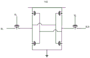
FIG. 2 is a circuit diagram of an SRAM cell according to the present embodiment.
Fig. 3 is a cross-sectional block diagram of a transistor in a typical fully depleted SOI configuration.
Detailed Description
The following describes in detail specific embodiments of the low power sram cell and the memory according to the present invention with reference to the drawings.
FIG. 2 is a circuit diagram of an SRAM cell according to the present embodiment, including: a first CMOS inverter consisting of a first N-type transistor N1 and a first P-type transistor P1, and a second CMOS inverter consisting of a second N-type transistor N2 and a second P-type transistor P2. The first and second CMOS inverters are arranged in an opposing interlocking arrangement. The output terminals Q and QB of the first and second CMOS inverters are connected to the sources of the third N-type transistor N3 and the fourth N-type transistor N4, respectively, and the drains of the other ends of the third N-type transistor N3 and the fourth N-type transistor N4 are used as the write bit line WBL and the write bit line bar signal WBLB. The above is a basic 6-transistor sram circuit diagram.
In this embodiment, the first to second P-type transistors and the first to fourth N-type transistors are all transistors having a fully depleted SOI structure. The fully depleted transistor is configured as shown in fig. 3, and the modulation effect of the back gate can increase or decrease the threshold voltage of the transistor.
The first N-type transistor N1 and the second N-type transistor N2 are back gate transistors, the back gates are connected to the read word line RWL, and the sources are grounded VSS; the first P-type transistor P1, the second P-type transistor P2, the third N-type transistor N3, and the fourth N-type transistor N4 are back gate transistors, the back gates being connected to the write word line WWL; the gates of the third N-type transistor N3 and the fourth N-type transistor N4 are also connected to the write word line WWL. The drains of the first P-type transistor P1 and the second P-type transistor P2 are connected to the operating voltage VDD, and form two CMOS inverters which are oppositely interlocked with the first N-type transistor N1 and the second N-type transistor N2.
In order to ensure that the static memory can maintain a good working state even under a low working voltage, the embodiment further includes a fifth N-type transistor N5 and a sixth N-type transistor N6. And the grid electrode of the fifth N-type transistor is connected with the input end of the first CMOS inverter, the source electrode of the fifth N-type transistor is connected with the drain electrode of the sixth N-type transistor, and the source electrode of the sixth N-type transistor is used as a read bit line RBL. The fifth N-type transistor N5 is a back gate transistor, and the back gate thereof is connected to the body gate; the sixth N-type transistor N6 is a back gate transistor, the back gate of which is connected to the body gate and connected to the read word line RWL.
In the circuit, during writing operation, the write word line WWL is at a high level, so that the threshold voltages of the first P-type transistor P1 and the second P-type transistor P2 are increased, and the threshold voltages of the third N-type transistor N and the fourth N-type transistor N4 are decreased, thereby enhancing the writing capability of the sram.
In the hold operation, both the write word line WWL and the read word line RWL are low, and the cell static power consumption is unchanged.
In a read operation, the read word line RWL is at a high level, and the threshold voltages of the first N-type transistor N1 and the second N-type transistor N2 are lowered. The read noise margin of the cell becomes large. When the stored data "0" is read (Q is 0 and QB is 1), the fifth N-type transistor N5 and the sixth N-type transistor N6 decrease in threshold voltage and the data "0" read current increases. When the storage data "1" is read (Q ═ 1, QB ═ 0), since the fifth N-type transistor N5 is in an off state, it functions as a large resistance. The data "1" read current does not vary much. The difference between the reading currents of the two data states is improved, and the data reading accuracy is improved.
In the description of the above embodiments, only one source/drain is described, and it should be noted that the source/drain of the transistor can be interchanged without affecting the basic function.
The foregoing is only a preferred embodiment of the present invention, and it should be noted that, for those skilled in the art, various modifications and decorations can be made without departing from the principle of the present invention, and these modifications and decorations should also be regarded as the protection scope of the present invention.
Claims (3)
1. A low power consumption static random access memory unit comprises a first CMOS inverter composed of a first N-type transistor and a first P-type transistor, a second CMOS inverter composed of a second N-type transistor and a second P-type transistor, the first and second CMOS inverters are oppositely arranged in an interlocking way, the output ends of the first and second CMOS inverters are respectively connected with the source/drain electrodes of a third N-type transistor and a fourth N-type transistor,
the first N-type transistor and the second N-type transistor are back gate transistors, and the back gates are connected with the read word line;
the first P-type transistor, the second P-type transistor, the third N-type transistor, and the fourth N-type transistor are back gate transistors, the back gates being connected to a write word line;
the grid electrode of the fifth N-type transistor is connected with the input end of the first CMOS inverter, and the source/drain electrode of the fifth N-type transistor is connected with the drain/source electrode of the sixth N-type transistor;
the fifth N-type transistor is a back gate transistor, and the back gate of the fifth N-type transistor is connected with the body gate;
the sixth N-type transistor is a back gate transistor, and the back gate of the sixth N-type transistor is connected with the body gate and connected to the read word line.
2. The low power consumption static random access memory cell according to claim 1, wherein the first to second P-type transistors and the first to sixth N-type transistors are all transistors of a fully depleted SOI structure.
3. A low power static random access memory cell comprising the static random access memory cell of any one of claims 1-3.
Priority Applications (1)
| Application Number | Priority Date | Filing Date | Title |
|---|---|---|---|
| CN202011595333.5A CN112687308A (en) | 2020-12-29 | 2020-12-29 | Low-power consumption static random access memory unit and memory |
Applications Claiming Priority (1)
| Application Number | Priority Date | Filing Date | Title |
|---|---|---|---|
| CN202011595333.5A CN112687308A (en) | 2020-12-29 | 2020-12-29 | Low-power consumption static random access memory unit and memory |
Publications (1)
| Publication Number | Publication Date |
|---|---|
| CN112687308A true CN112687308A (en) | 2021-04-20 |
Family
ID=75455278
Family Applications (1)
| Application Number | Title | Priority Date | Filing Date |
|---|---|---|---|
| CN202011595333.5A Pending CN112687308A (en) | 2020-12-29 | 2020-12-29 | Low-power consumption static random access memory unit and memory |
Country Status (1)
| Country | Link |
|---|---|
| CN (1) | CN112687308A (en) |
Cited By (2)
| Publication number | Priority date | Publication date | Assignee | Title |
|---|---|---|---|---|
| CN113628649A (en) * | 2021-06-16 | 2021-11-09 | 杭州未名信科科技有限公司 | Static random access memory unit structure and static random access memory |
| CN113642706A (en) * | 2021-08-10 | 2021-11-12 | 中国科学院上海微系统与信息技术研究所 | Neuron network unit, convolution operation module and convolution neural network |
Citations (9)
| Publication number | Priority date | Publication date | Assignee | Title |
|---|---|---|---|---|
| EP0801397A2 (en) * | 1996-04-08 | 1997-10-15 | Texas Instruments Inc. | Improvements in or relating to semiconductor memory devices |
| US20120307548A1 (en) * | 2011-06-01 | 2012-12-06 | National Chiao Tung University | Dual-port subthreshold sram cell |
| US20130170288A1 (en) * | 2011-12-29 | 2013-07-04 | Stmicroelectronics Pvt. Ltd. | Dual port register file memory cell with reduced susceptibility to noise during same row access |
| US20150371702A1 (en) * | 2014-06-18 | 2015-12-24 | Taiwan Semiconductor Manufacturing Company, Ltd. | Static random access memory and method of using the same |
| US9336861B1 (en) * | 2014-08-12 | 2016-05-10 | Skan Technologies Corporation | Static random access memory (SRAM) bitcell and memory architecture without a write bitline |
| CN109658960A (en) * | 2018-12-10 | 2019-04-19 | 安徽大学 | A kind of 12T TFET SRAM cell circuit for writing nargin with super low-power consumption and height |
| CN110189780A (en) * | 2019-04-29 | 2019-08-30 | 安徽大学 | A kind of circuit structure of tunneling field-effect transistor static random access memory cell |
| US20200082876A1 (en) * | 2018-09-12 | 2020-03-12 | Nxp B.V. | Transistor body bias control circuit for sram cells |
| CN111145810A (en) * | 2019-12-19 | 2020-05-12 | 华东师范大学 | Static random access memory based on FDSOI device back gate structure |
-
2020
- 2020-12-29 CN CN202011595333.5A patent/CN112687308A/en active Pending
Patent Citations (9)
| Publication number | Priority date | Publication date | Assignee | Title |
|---|---|---|---|---|
| EP0801397A2 (en) * | 1996-04-08 | 1997-10-15 | Texas Instruments Inc. | Improvements in or relating to semiconductor memory devices |
| US20120307548A1 (en) * | 2011-06-01 | 2012-12-06 | National Chiao Tung University | Dual-port subthreshold sram cell |
| US20130170288A1 (en) * | 2011-12-29 | 2013-07-04 | Stmicroelectronics Pvt. Ltd. | Dual port register file memory cell with reduced susceptibility to noise during same row access |
| US20150371702A1 (en) * | 2014-06-18 | 2015-12-24 | Taiwan Semiconductor Manufacturing Company, Ltd. | Static random access memory and method of using the same |
| US9336861B1 (en) * | 2014-08-12 | 2016-05-10 | Skan Technologies Corporation | Static random access memory (SRAM) bitcell and memory architecture without a write bitline |
| US20200082876A1 (en) * | 2018-09-12 | 2020-03-12 | Nxp B.V. | Transistor body bias control circuit for sram cells |
| CN109658960A (en) * | 2018-12-10 | 2019-04-19 | 安徽大学 | A kind of 12T TFET SRAM cell circuit for writing nargin with super low-power consumption and height |
| CN110189780A (en) * | 2019-04-29 | 2019-08-30 | 安徽大学 | A kind of circuit structure of tunneling field-effect transistor static random access memory cell |
| CN111145810A (en) * | 2019-12-19 | 2020-05-12 | 华东师范大学 | Static random access memory based on FDSOI device back gate structure |
Cited By (2)
| Publication number | Priority date | Publication date | Assignee | Title |
|---|---|---|---|---|
| CN113628649A (en) * | 2021-06-16 | 2021-11-09 | 杭州未名信科科技有限公司 | Static random access memory unit structure and static random access memory |
| CN113642706A (en) * | 2021-08-10 | 2021-11-12 | 中国科学院上海微系统与信息技术研究所 | Neuron network unit, convolution operation module and convolution neural network |
Similar Documents
| Publication | Publication Date | Title |
|---|---|---|
| US7633315B2 (en) | Semiconductor integrated circuit device | |
| JP5656875B2 (en) | Low leakage high performance static random access memory cells using dual technology transistors. | |
| TWI485705B (en) | Memory cells having a row-based read and/or write support circuitry | |
| US7313012B2 (en) | Back-gate controlled asymmetrical memory cell and memory using the cell | |
| US9111638B2 (en) | SRAM bit cell with reduced bit line pre-charge voltage | |
| CN109658960B (en) | 12T TFET SRAM cell circuit with ultralow power consumption and high write margin | |
| Wang et al. | A 45nm dual-port SRAM with write and read capability enhancement at low voltage | |
| KR970023375A (en) | Data holding circuit | |
| JP5237504B2 (en) | Subthreshold memory cell circuit with high density and high robustness | |
| CN107240416B (en) | Sub-threshold SRAM memory cell circuit | |
| CN110767251B (en) | 11T TFET SRAM unit circuit structure with low power consumption and high write margin | |
| CN112687308A (en) | Low-power consumption static random access memory unit and memory | |
| US10276578B2 (en) | Dynamic oxide semiconductor random access memory(DOSRAM) having a capacitor electrically connected to the random access memory (SRAM) | |
| CN112530491A (en) | Static random access memory device | |
| US7471546B2 (en) | Hierarchical six-transistor SRAM | |
| CN110379448B (en) | 9T TFET and MOSFET device hybrid SRAM cell circuit with high write margin | |
| CN101840728B (en) | Dual-end static random access memory (SRMA) unit | |
| US20170194037A1 (en) | Digtial circuit structures to control leakage current | |
| US20180233194A1 (en) | Storage Bitcell | |
| CN209880162U (en) | Hybrid 10T TFET-MOSFET SRAM cell circuit with low power consumption and write enhancement | |
| CN110232941B (en) | Hybrid 10T TFET-MOSFET SRAM cell circuit with low power consumption and write enhancement | |
| CN110675905A (en) | 12T TFET SRAM unit circuit structure with high stability | |
| CN113628650B (en) | SRAM cell structure and SRAM | |
| CN112634957A (en) | Low-power consumption static random access memory unit and memory | |
| CN113628649A (en) | Static random access memory unit structure and static random access memory |
Legal Events
| Date | Code | Title | Description |
|---|---|---|---|
| PB01 | Publication | ||
| PB01 | Publication | ||
| SE01 | Entry into force of request for substantive examination | ||
| SE01 | Entry into force of request for substantive examination |