CN1126064C - 具有用焊接线连接的天线的无触点卡的制造方法 - Google Patents
具有用焊接线连接的天线的无触点卡的制造方法 Download PDFInfo
- Publication number
- CN1126064C CN1126064C CN98805380A CN98805380A CN1126064C CN 1126064 C CN1126064 C CN 1126064C CN 98805380 A CN98805380 A CN 98805380A CN 98805380 A CN98805380 A CN 98805380A CN 1126064 C CN1126064 C CN 1126064C
- Authority
- CN
- China
- Prior art keywords
- chip
- lead
- contact
- antenna
- welded
- Prior art date
- Legal status (The legal status is an assumption and is not a legal conclusion. Google has not performed a legal analysis and makes no representation as to the accuracy of the status listed.)
- Expired - Fee Related
Links
Images


Classifications
-
- G—PHYSICS
- G06—COMPUTING; CALCULATING OR COUNTING
- G06K—GRAPHICAL DATA READING; PRESENTATION OF DATA; RECORD CARRIERS; HANDLING RECORD CARRIERS
- G06K19/00—Record carriers for use with machines and with at least a part designed to carry digital markings
- G06K19/06—Record carriers for use with machines and with at least a part designed to carry digital markings characterised by the kind of the digital marking, e.g. shape, nature, code
- G06K19/067—Record carriers with conductive marks, printed circuits or semiconductor circuit elements, e.g. credit or identity cards also with resonating or responding marks without active components
- G06K19/07—Record carriers with conductive marks, printed circuits or semiconductor circuit elements, e.g. credit or identity cards also with resonating or responding marks without active components with integrated circuit chips
- G06K19/077—Constructional details, e.g. mounting of circuits in the carrier
- G06K19/07749—Constructional details, e.g. mounting of circuits in the carrier the record carrier being capable of non-contact communication, e.g. constructional details of the antenna of a non-contact smart card
- G06K19/0775—Constructional details, e.g. mounting of circuits in the carrier the record carrier being capable of non-contact communication, e.g. constructional details of the antenna of a non-contact smart card arrangements for connecting the integrated circuit to the antenna
-
- G—PHYSICS
- G06—COMPUTING; CALCULATING OR COUNTING
- G06K—GRAPHICAL DATA READING; PRESENTATION OF DATA; RECORD CARRIERS; HANDLING RECORD CARRIERS
- G06K19/00—Record carriers for use with machines and with at least a part designed to carry digital markings
- G06K19/06—Record carriers for use with machines and with at least a part designed to carry digital markings characterised by the kind of the digital marking, e.g. shape, nature, code
- G06K19/067—Record carriers with conductive marks, printed circuits or semiconductor circuit elements, e.g. credit or identity cards also with resonating or responding marks without active components
- G06K19/07—Record carriers with conductive marks, printed circuits or semiconductor circuit elements, e.g. credit or identity cards also with resonating or responding marks without active components with integrated circuit chips
- G06K19/077—Constructional details, e.g. mounting of circuits in the carrier
- G06K19/07749—Constructional details, e.g. mounting of circuits in the carrier the record carrier being capable of non-contact communication, e.g. constructional details of the antenna of a non-contact smart card
-
- H—ELECTRICITY
- H01—ELECTRIC ELEMENTS
- H01L—SEMICONDUCTOR DEVICES NOT COVERED BY CLASS H10
- H01L23/00—Details of semiconductor or other solid state devices
- H01L23/48—Arrangements for conducting electric current to or from the solid state body in operation, e.g. leads, terminal arrangements ; Selection of materials therefor
- H01L23/488—Arrangements for conducting electric current to or from the solid state body in operation, e.g. leads, terminal arrangements ; Selection of materials therefor consisting of soldered or bonded constructions
- H01L23/498—Leads, i.e. metallisations or lead-frames on insulating substrates, e.g. chip carriers
- H01L23/49855—Leads, i.e. metallisations or lead-frames on insulating substrates, e.g. chip carriers for flat-cards, e.g. credit cards
-
- H—ELECTRICITY
- H01—ELECTRIC ELEMENTS
- H01L—SEMICONDUCTOR DEVICES NOT COVERED BY CLASS H10
- H01L23/00—Details of semiconductor or other solid state devices
- H01L23/58—Structural electrical arrangements for semiconductor devices not otherwise provided for, e.g. in combination with batteries
- H01L23/64—Impedance arrangements
- H01L23/645—Inductive arrangements
-
- H—ELECTRICITY
- H01—ELECTRIC ELEMENTS
- H01L—SEMICONDUCTOR DEVICES NOT COVERED BY CLASS H10
- H01L2224/00—Indexing scheme for arrangements for connecting or disconnecting semiconductor or solid-state bodies and methods related thereto as covered by H01L24/00
- H01L2224/01—Means for bonding being attached to, or being formed on, the surface to be connected, e.g. chip-to-package, die-attach, "first-level" interconnects; Manufacturing methods related thereto
- H01L2224/10—Bump connectors; Manufacturing methods related thereto
- H01L2224/15—Structure, shape, material or disposition of the bump connectors after the connecting process
- H01L2224/16—Structure, shape, material or disposition of the bump connectors after the connecting process of an individual bump connector
-
- H—ELECTRICITY
- H01—ELECTRIC ELEMENTS
- H01L—SEMICONDUCTOR DEVICES NOT COVERED BY CLASS H10
- H01L2224/00—Indexing scheme for arrangements for connecting or disconnecting semiconductor or solid-state bodies and methods related thereto as covered by H01L24/00
- H01L2224/01—Means for bonding being attached to, or being formed on, the surface to be connected, e.g. chip-to-package, die-attach, "first-level" interconnects; Manufacturing methods related thereto
- H01L2224/42—Wire connectors; Manufacturing methods related thereto
- H01L2224/44—Structure, shape, material or disposition of the wire connectors prior to the connecting process
- H01L2224/45—Structure, shape, material or disposition of the wire connectors prior to the connecting process of an individual wire connector
- H01L2224/45001—Core members of the connector
- H01L2224/4501—Shape
- H01L2224/45012—Cross-sectional shape
- H01L2224/45015—Cross-sectional shape being circular
-
- H—ELECTRICITY
- H01—ELECTRIC ELEMENTS
- H01L—SEMICONDUCTOR DEVICES NOT COVERED BY CLASS H10
- H01L2224/00—Indexing scheme for arrangements for connecting or disconnecting semiconductor or solid-state bodies and methods related thereto as covered by H01L24/00
- H01L2224/01—Means for bonding being attached to, or being formed on, the surface to be connected, e.g. chip-to-package, die-attach, "first-level" interconnects; Manufacturing methods related thereto
- H01L2224/42—Wire connectors; Manufacturing methods related thereto
- H01L2224/44—Structure, shape, material or disposition of the wire connectors prior to the connecting process
- H01L2224/45—Structure, shape, material or disposition of the wire connectors prior to the connecting process of an individual wire connector
- H01L2224/45001—Core members of the connector
- H01L2224/45099—Material
- H01L2224/451—Material with a principal constituent of the material being a metal or a metalloid, e.g. boron (B), silicon (Si), germanium (Ge), arsenic (As), antimony (Sb), tellurium (Te) and polonium (Po), and alloys thereof
- H01L2224/45117—Material with a principal constituent of the material being a metal or a metalloid, e.g. boron (B), silicon (Si), germanium (Ge), arsenic (As), antimony (Sb), tellurium (Te) and polonium (Po), and alloys thereof the principal constituent melting at a temperature of greater than or equal to 400°C and less than 950°C
- H01L2224/45124—Aluminium (Al) as principal constituent
-
- H—ELECTRICITY
- H01—ELECTRIC ELEMENTS
- H01L—SEMICONDUCTOR DEVICES NOT COVERED BY CLASS H10
- H01L2224/00—Indexing scheme for arrangements for connecting or disconnecting semiconductor or solid-state bodies and methods related thereto as covered by H01L24/00
- H01L2224/01—Means for bonding being attached to, or being formed on, the surface to be connected, e.g. chip-to-package, die-attach, "first-level" interconnects; Manufacturing methods related thereto
- H01L2224/42—Wire connectors; Manufacturing methods related thereto
- H01L2224/44—Structure, shape, material or disposition of the wire connectors prior to the connecting process
- H01L2224/45—Structure, shape, material or disposition of the wire connectors prior to the connecting process of an individual wire connector
- H01L2224/45001—Core members of the connector
- H01L2224/45099—Material
- H01L2224/451—Material with a principal constituent of the material being a metal or a metalloid, e.g. boron (B), silicon (Si), germanium (Ge), arsenic (As), antimony (Sb), tellurium (Te) and polonium (Po), and alloys thereof
- H01L2224/45138—Material with a principal constituent of the material being a metal or a metalloid, e.g. boron (B), silicon (Si), germanium (Ge), arsenic (As), antimony (Sb), tellurium (Te) and polonium (Po), and alloys thereof the principal constituent melting at a temperature of greater than or equal to 950°C and less than 1550°C
- H01L2224/45144—Gold (Au) as principal constituent
-
- H—ELECTRICITY
- H01—ELECTRIC ELEMENTS
- H01L—SEMICONDUCTOR DEVICES NOT COVERED BY CLASS H10
- H01L2224/00—Indexing scheme for arrangements for connecting or disconnecting semiconductor or solid-state bodies and methods related thereto as covered by H01L24/00
- H01L2224/01—Means for bonding being attached to, or being formed on, the surface to be connected, e.g. chip-to-package, die-attach, "first-level" interconnects; Manufacturing methods related thereto
- H01L2224/42—Wire connectors; Manufacturing methods related thereto
- H01L2224/44—Structure, shape, material or disposition of the wire connectors prior to the connecting process
- H01L2224/45—Structure, shape, material or disposition of the wire connectors prior to the connecting process of an individual wire connector
- H01L2224/45001—Core members of the connector
- H01L2224/45099—Material
- H01L2224/451—Material with a principal constituent of the material being a metal or a metalloid, e.g. boron (B), silicon (Si), germanium (Ge), arsenic (As), antimony (Sb), tellurium (Te) and polonium (Po), and alloys thereof
- H01L2224/45138—Material with a principal constituent of the material being a metal or a metalloid, e.g. boron (B), silicon (Si), germanium (Ge), arsenic (As), antimony (Sb), tellurium (Te) and polonium (Po), and alloys thereof the principal constituent melting at a temperature of greater than or equal to 950°C and less than 1550°C
- H01L2224/45147—Copper (Cu) as principal constituent
-
- H—ELECTRICITY
- H01—ELECTRIC ELEMENTS
- H01L—SEMICONDUCTOR DEVICES NOT COVERED BY CLASS H10
- H01L2224/00—Indexing scheme for arrangements for connecting or disconnecting semiconductor or solid-state bodies and methods related thereto as covered by H01L24/00
- H01L2224/01—Means for bonding being attached to, or being formed on, the surface to be connected, e.g. chip-to-package, die-attach, "first-level" interconnects; Manufacturing methods related thereto
- H01L2224/42—Wire connectors; Manufacturing methods related thereto
- H01L2224/47—Structure, shape, material or disposition of the wire connectors after the connecting process
- H01L2224/48—Structure, shape, material or disposition of the wire connectors after the connecting process of an individual wire connector
- H01L2224/4805—Shape
- H01L2224/4809—Loop shape
- H01L2224/48091—Arched
-
- H—ELECTRICITY
- H01—ELECTRIC ELEMENTS
- H01L—SEMICONDUCTOR DEVICES NOT COVERED BY CLASS H10
- H01L24/00—Arrangements for connecting or disconnecting semiconductor or solid-state bodies; Methods or apparatus related thereto
- H01L24/01—Means for bonding being attached to, or being formed on, the surface to be connected, e.g. chip-to-package, die-attach, "first-level" interconnects; Manufacturing methods related thereto
- H01L24/42—Wire connectors; Manufacturing methods related thereto
- H01L24/44—Structure, shape, material or disposition of the wire connectors prior to the connecting process
- H01L24/45—Structure, shape, material or disposition of the wire connectors prior to the connecting process of an individual wire connector
-
- H—ELECTRICITY
- H01—ELECTRIC ELEMENTS
- H01L—SEMICONDUCTOR DEVICES NOT COVERED BY CLASS H10
- H01L24/00—Arrangements for connecting or disconnecting semiconductor or solid-state bodies; Methods or apparatus related thereto
- H01L24/01—Means for bonding being attached to, or being formed on, the surface to be connected, e.g. chip-to-package, die-attach, "first-level" interconnects; Manufacturing methods related thereto
- H01L24/42—Wire connectors; Manufacturing methods related thereto
- H01L24/47—Structure, shape, material or disposition of the wire connectors after the connecting process
- H01L24/48—Structure, shape, material or disposition of the wire connectors after the connecting process of an individual wire connector
-
- H—ELECTRICITY
- H01—ELECTRIC ELEMENTS
- H01L—SEMICONDUCTOR DEVICES NOT COVERED BY CLASS H10
- H01L2924/00—Indexing scheme for arrangements or methods for connecting or disconnecting semiconductor or solid-state bodies as covered by H01L24/00
- H01L2924/0001—Technical content checked by a classifier
- H01L2924/00011—Not relevant to the scope of the group, the symbol of which is combined with the symbol of this group
-
- H—ELECTRICITY
- H01—ELECTRIC ELEMENTS
- H01L—SEMICONDUCTOR DEVICES NOT COVERED BY CLASS H10
- H01L2924/00—Indexing scheme for arrangements or methods for connecting or disconnecting semiconductor or solid-state bodies as covered by H01L24/00
- H01L2924/01—Chemical elements
- H01L2924/01013—Aluminum [Al]
-
- H—ELECTRICITY
- H01—ELECTRIC ELEMENTS
- H01L—SEMICONDUCTOR DEVICES NOT COVERED BY CLASS H10
- H01L2924/00—Indexing scheme for arrangements or methods for connecting or disconnecting semiconductor or solid-state bodies as covered by H01L24/00
- H01L2924/01—Chemical elements
- H01L2924/01014—Silicon [Si]
-
- H—ELECTRICITY
- H01—ELECTRIC ELEMENTS
- H01L—SEMICONDUCTOR DEVICES NOT COVERED BY CLASS H10
- H01L2924/00—Indexing scheme for arrangements or methods for connecting or disconnecting semiconductor or solid-state bodies as covered by H01L24/00
- H01L2924/01—Chemical elements
- H01L2924/0105—Tin [Sn]
-
- H—ELECTRICITY
- H01—ELECTRIC ELEMENTS
- H01L—SEMICONDUCTOR DEVICES NOT COVERED BY CLASS H10
- H01L2924/00—Indexing scheme for arrangements or methods for connecting or disconnecting semiconductor or solid-state bodies as covered by H01L24/00
- H01L2924/01—Chemical elements
- H01L2924/01057—Lanthanum [La]
-
- H—ELECTRICITY
- H01—ELECTRIC ELEMENTS
- H01L—SEMICONDUCTOR DEVICES NOT COVERED BY CLASS H10
- H01L2924/00—Indexing scheme for arrangements or methods for connecting or disconnecting semiconductor or solid-state bodies as covered by H01L24/00
- H01L2924/01—Chemical elements
- H01L2924/01058—Cerium [Ce]
-
- H—ELECTRICITY
- H01—ELECTRIC ELEMENTS
- H01L—SEMICONDUCTOR DEVICES NOT COVERED BY CLASS H10
- H01L2924/00—Indexing scheme for arrangements or methods for connecting or disconnecting semiconductor or solid-state bodies as covered by H01L24/00
- H01L2924/01—Chemical elements
- H01L2924/01079—Gold [Au]
-
- H—ELECTRICITY
- H01—ELECTRIC ELEMENTS
- H01L—SEMICONDUCTOR DEVICES NOT COVERED BY CLASS H10
- H01L2924/00—Indexing scheme for arrangements or methods for connecting or disconnecting semiconductor or solid-state bodies as covered by H01L24/00
- H01L2924/10—Details of semiconductor or other solid state devices to be connected
- H01L2924/11—Device type
- H01L2924/14—Integrated circuits
Landscapes
- Engineering & Computer Science (AREA)
- Microelectronics & Electronic Packaging (AREA)
- Physics & Mathematics (AREA)
- General Physics & Mathematics (AREA)
- Computer Hardware Design (AREA)
- Theoretical Computer Science (AREA)
- Condensed Matter Physics & Semiconductors (AREA)
- Power Engineering (AREA)
- Credit Cards Or The Like (AREA)
Abstract
本发明涉及无触点芯片卡。为了有助于将集成电路芯片安装到无触点芯片卡上、尤其是将芯片与卡中的天线相连接,根据本发明,在芯片的触点(12a,12b)上焊接金线(30),至少金线的一端从芯片上突起。最好当芯片仍是半导体晶片的一部分时焊接导线(30)。导线可被焊在同一芯片的两个触点之间;导线也可被焊在属于两个相邻芯片的两个触点之间并在晶片切割操作时被切割成单个芯片。当将芯片安装到卡上时,将芯片压接到天线上,以使得焊接导线与线绕天线或印刷天线导体的端部形成连接。
Description
本发明涉及芯片卡的制造,更具体地,涉及能借助集成于卡上的天线无触点地工作的卡的制造。
这类卡可用于实现不同操作,例如:银行业务,电话通信,识别操作,记帐业务或充存支付货币单位,及可通过发射-接收终端及放置在这个终端作用范围内的卡之间的高频电磁耦合远距离执行的各种操作。
在制造这种卡时应解决的一个主要技术问题是,天线与保证卡的电子功能的集成电路芯卡的连接。在该制造中显然应该考虑传统的机械强度、可靠性及制造成本上的限制。
本发明之目的在于提供一种制造方法,它能最佳地解决芯片与天线之间电连接的问题。
为此,本发明建议:在第一阶段,制造设有至少一部分焊在芯片上的导线的集成电路芯片,该导线具有相对芯片表面的突起部分;及接着在第二阶段,通过将突起部分施加在天线导体的一个端点上使芯片及天线导体形成接触,以致在天线及焊接线之间建立直接电接触。
换句话说,使用非常传统的“线焊”或用热压焊接导线,这就是说在一个芯片上焊接导线(通常为金或铝导线),但是不是以通常方式使用该技术,即为,使导线从芯片的触点上伸出,以便将其引到芯片支持部件(通常为接线栅或印刷电路组件)的触点上,我们将导线的一端焊在芯片的触点上,但不将其另一端焊到该芯片应转接到外部元件上。该导线保持自由,以便用作从芯片上面伸出的接触件。
因此,本发明提供了一种制造包括集成电路芯片及天线的无触点芯片卡的方法,其特征在于:在初始步骤中将至少一根导线焊到芯片触点上而不将其进一步焊到芯片支持部件上,在下一步骤中,将建立焊接导线及天线导体一个端部之间的直接电接触。
可以考虑到实施该方法的各种方式。在第一种实施方式中,焊接导线的第一端被焊在芯片触点上及第二端保持自由,以使得导线的固有弹性能有助于导线和天线形成接触。在另一实施方式中,导线被焊到芯片的两个触点上,位于两触点之间的导线部分从芯片上面伸出。这里也是导线的弹性有助于与天线导体的接触。在第三种实施方式中,在芯片上方导线被截成非常短,以致实际上它仅在触点上留下被压平的金属珠(这就是说,该珠通常是由焊接装置热压时焊头形成的),但是该珠足够地凸出,以便能与天线导体接触。
导线的焊接操作最好当芯片仍为晶片的的一部分时进行,该晶片将在随后被切成单个芯片(而传统的用于与外部支持件连接的“线焊技术”总是用于已切下的芯片上并准备好待安装到组件中)。
从对以下结合附图作出的详细说明的阅读将使本发明的其它特征及优点显现出来,附图为:
图1表示在其上已集成了多个用于芯片卡的电路的半导体晶片的顶视图;
图2表示晶片上并列芯片的放大顶视图,其中每个芯片具有两个触点;
图3表示借助切割路径中的触点用金线连接两个相邻芯片的触点的晶片上芯片的顶视图;
图4表示与图3相对应的侧向截面图;
图5表示带有伸出的并具有一个自由端的焊接导线的、被切下的芯片;
图6表示将一个芯片安装到卡上并与线圈天线相连接;
图7表示一个芯片与一个印刷天线相安装;
图8表示其中每根导线被焊到芯片中两个触点上的一个变型实施方式;
图9及10表示本方法的另一种变型,其中焊接导线被齐根切割到与导线焊接装置形成的焊珠齐平。
在图1中表示出一个半导体晶片10,在其上以传统方式作成用于在随后被分割成单个芯片的集成电路。允许构成单个芯片的切割区域用虚线表示。
图2表示具有几个并列芯片12、14,16,18的放大图,这些并列芯片被垂直切割路径20及水平切割路径22分开。
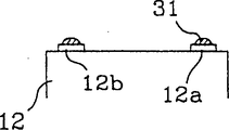
每个芯片上设有两个触点,它们允许根据传统的“线焊”(“Wire-bonding”)技术焊上金线或铝线。对于每个芯片这些触点用下标a及b表示,这就是说,芯片12包括两个触点12a及12b。最好设在位于两个相邻芯片之间的切割路径中也设置一个中间触点,该触点位于直接面对的两个触点之间,这两个触点的每个各属于相邻的两个芯片中的一个。因此,中间触点24位于芯片12及14的触点12a及14b之间,及中间触点26位于芯片16及18的触点16a及18b之间。这些触点不是强制地需要的,但是非常有利于随后的切割。
图3表示根据“线焊”技术设置焊接导线。这种导线通常是金线,但也可以是铝线。导线30被焊在一个芯片的触点(例如触点12a)上,并朝着相邻的中间触点24,后者用于中转保持,该导线被焊到该中间触点24上并再朝着相邻芯片14的触点14a。
应该指出,被称为“线焊”的并用于全世界生产的90%以上的集成电路的传统导线焊接技术在于:借助焊接头在具有热的状态下施加压力(热压焊接)使金线或铝线以珠形端部压接在芯片触点上,并在可能的情况下使用超声波振动;然后,不切断导线,借助焊头将导线引到另一焊点上,后者在现有技术中通常为一个芯片支持部件(接线栅或印刷电路);接着将该导线焊到该第二触点上;最后在紧接着该第二次焊接操作后将熔化的金属珠留在导线端部,以便新的焊接操作。
在本发明中,焊接操作在于:将导线焊到一个芯片的一个触点上,将该导线引导到中间触点上,并将该导线焊到该触点上,及再将其引导到一个相邻芯片的触点上,以便在切断导线前进行一次新的焊接操作。因此,在将半导体晶片切割成单个芯片前,在该半导体晶片卡进行了导线焊接的全部操作。
图4表示导线安装的截面图。切割路径20可由相对于芯片上表面的凹陷部分构成,并考虑到导线焊接操作前在晶片进行的沉积及蚀刻操作。
接下来的操作是将晶片切割成单个芯片。该切割原则上是用锯完成的,及在该操作时焊接导线被切断。锯线的宽度为切割路径20的宽度。在锯断时位于该路径中的中间触点24、26将消失,但是它们在锯芯片操作时具有保持导线的有益作用。以此方式将有助于导线的锯割。图5表示锯割结果的芯片侧向截面图;导线30已被切断及它们的端部保持自由。
这时芯片即可被安装到包含天线的无触点卡上。该天线可由绕成线圈的导线构成亦或由印在绝缘片或板上的导体构成。
在第一种情况下,由图6所示,我们可以这样地处理:将具有其金线30的芯片12用胶粘贴在希望制作的卡形式的塑性材料40的卡或板的表面。该胶是一种非导电胶。芯片的有源正面,即常有触点及金线的一面被压在板的该表面上。焊接导线30的端部由于它们的弹性而伸过芯片的边缘。
然后,将绕成线圈的导线天线50粘贴塑性材料的片40上,以使得线圈天线的端部50a、50b被压在焊接导线30上并在天线的线圈导线(它可由铜制成)及焊接导线之间建立直接的电接触。这时可通过用导电胶滴的粘接或用锡焊在金线及铜线之间维持该接触。
然后可将一个第二塑性材料片60施加在这操作成的组件的顶部,并用胶或热层压、或冷层压加以固定,以便封闭芯片及天线并由此形成无触点卡。
如果天线是以绝缘衬底上的印刷导线形式实施时,安装将如图7所示方式进行:绝缘衬底例如是塑料片42(尤其为PVC),上面覆盖了一层丝网印刷或蚀刻成天线形式的金属层。天线导体的端部44a、44b隔开一段距离,该距离大致相当于芯片的焊接导线30自由端部之间的距离。将芯片的正面用非导电胶46朝着片42的金属化表面粘接,以使得芯片上焊接导线压在天线导体的端部;非导电胶不能被施加得阻止在焊接导线及天线之间形成电接触。然后可在焊接导线上施加导电胶48,以保证电接触的维持。接着可通过胶粘或热层压、或冷层压施加第二塑料片60来封闭芯片并形成无触点卡。
在图6及7的实施方式中,芯片的晶片最好覆盖非导电胶或另外的绝缘覆盖层(清漆或其它层),以便使导电胶不会在天线导体及芯片之间建立不希望有的接触。
一般地,在上述所有实施方式中,可以考虑使用各向异性的导电胶来代替导电胶及非导电胶,该各向异性的导电胶在胶层的厚度方向上具有导电性能,而在层的平面方向上无导电性能。在此情况下,各向异性导电胶可以同时取代导电胶及非导电胶,以便能用单一步骤而非两个步骤实现粘接,而不会有不希望的短路危险。
在图8以正面图及侧面图表示的变型实施方式中,焊接到芯片上并将用于建立接触的导线没有切断的自由端:每个导线的两端被焊在该芯片上隔开的两个触点上,用来建立接触的是这两个端部之间的突起部分。在芯片被锯下时,这些导线不位于切割路径中,因此不会被切断。在切割路径中也就不必设置中间触点。此外,在此情况下可在将半导体晶片锯成单个芯片前或后,焊接金线或铝线。
该图8的实施方式,相对于与线圈天线导线连接,更适于与印刷天线连接。天线及芯片之间的固定方式最好是锡焊而非用导电胶粘接,后者将有不希望的接触危险的诸多问题。在此情况下也可使用各向异性胶。
在上述各种实施方式中,可有利地设置:在芯片正面积沉一种保护及保持树脂滴。该树脂尤其在随后的锯切和安装操作时能更好地保持焊接导线。因此,该树脂滴最好在锯晶片前被沉积到每个芯片上。
在另一变型实施方式中,在芯片之间的切割路径中不使用中间触点。金线被相对地张紧在一个芯片的一个触点及相邻芯片的相对触点之间。假定在触点上焊接导线的操作在焊点上形成焊珠并且导线被削弱的区域正好在焊珠上方,则锯芯片的操作将正好在焊珠上方拉断导线,焊珠单独地留在触点上。
图9以更加放大的横截面的方式表示导线30,它在切割路径的上方连接着一个芯片12的触点12a及相邻芯片14的触点14a。焊接导线在每个触点上形成焊珠31,33,及正好在焊珠上方的薄弱区域35,37。
图10表示在锯断后的芯片12及14,它们包括仅由如31所示的金或铝、焊珠构成的通过“线焊”焊接的导线。芯片被粘接在天线导体端部,并最好用各向异性导电胶粘接。
Claims (10)
1.制造包括集成电路芯片(12)及天线(50)的无触点芯片卡的方法,其特征在于:在一个初始步骤中借助“线焊”技术将至少一根导线(30)焊接在芯片的一个触点(12a)以及另一触点(14b;24)之间,以及在下一步骤中,在已被焊在芯片的所述触点(12a)上的导线(30)的至少一部分及天线导体一个端部(50a、50b)之间建立直接电接触。
2.根据权利要求1的方法,其特征在于:在触点上的焊接导线具有相对芯片表面的一个突起部分,及在实施焊接导线及天线导体端部之间电接触的步骤时,将突起部分施加在该端部上。
3.根据权利要求1或2的方法,其特征在于:当芯片还是半导体晶片(10)的一部分时导线(30)被进行焊接,其中通过锯切随后形成各芯片。
4.根据权利要求3的方法,其特征在于:导线被焊接在晶片上一个芯片(12)的一个触点(12a)及相邻芯片(14)的一个触点(14b)之间。
5.根据权利要求4的方法,其特征在于:导线(30)借助于设在芯片之间的切割路径中的一个附加触点(24)被焊在两个相邻芯片的触点(12a,14b)之间。
6.根据权利要求4或5的方法,其特征在于:在锯切操作时导线(30)被割断,其中晶片被切割成各芯片单元,导线的一端保持自由并从芯片上突起,而导线的另一端焊在芯片的一个触点上。
7.根据权利要求1的方法,其特征在于:导线被焊在同一芯片的两个触点之间,位于两个触点之间的导线部分从芯片上突起。
8.根据权利要求1的方法,其特征在于:导线被焊在两个相邻的芯片之间,及在锯切操作时导线正好在焊在芯片触点上的焊珠(31,33)上方被拉断,该焊珠凸出芯片表面,以便与天线导体的端部相接触。
9.根据权利要求1的方法,其特征在于:设有焊接导线的芯片被粘贴在塑性材料的片(40)上,以及将一个作成导线线圈的天线粘在该片上,至少天线导线的一端(50a,50b)被压接在芯片的焊接导线上。
10.根据权利要求1的方法,其特征在于:设有焊接导线的芯片被粘贴在带有印刷天线导体的塑性材料的片(42)上,焊接导线被压接在天线导体的端部上。
Applications Claiming Priority (2)
| Application Number | Priority Date | Filing Date | Title |
|---|---|---|---|
| FR97/03630 | 1997-03-25 | ||
| FR9703630A FR2761527B1 (fr) | 1997-03-25 | 1997-03-25 | Procede de fabrication de carte sans contact avec connexion d'antenne par fils soudes |
Publications (2)
| Publication Number | Publication Date |
|---|---|
| CN1257597A CN1257597A (zh) | 2000-06-21 |
| CN1126064C true CN1126064C (zh) | 2003-10-29 |
Family
ID=9505163
Family Applications (1)
| Application Number | Title | Priority Date | Filing Date |
|---|---|---|---|
| CN98805380A Expired - Fee Related CN1126064C (zh) | 1997-03-25 | 1998-02-27 | 具有用焊接线连接的天线的无触点卡的制造方法 |
Country Status (11)
| Country | Link |
|---|---|
| US (1) | US6566163B1 (zh) |
| EP (1) | EP0972268B1 (zh) |
| JP (1) | JP2001518220A (zh) |
| KR (1) | KR20010005659A (zh) |
| CN (1) | CN1126064C (zh) |
| AU (1) | AU735725B2 (zh) |
| CA (1) | CA2283689A1 (zh) |
| DE (1) | DE69805404T2 (zh) |
| ES (1) | ES2176994T3 (zh) |
| FR (1) | FR2761527B1 (zh) |
| WO (1) | WO1998043205A1 (zh) |
Families Citing this family (19)
| Publication number | Priority date | Publication date | Assignee | Title |
|---|---|---|---|---|
| FR2795235B1 (fr) * | 1999-06-15 | 2002-08-02 | Gemplus Card Int | Procede de realisation de dispositifs comprenant une puce associee a un element de circuit et dispositifs obtenus |
| DE19948555A1 (de) * | 1999-12-03 | 2001-05-03 | Andreas Plettner | Verfahren zur Herstellung kontaktloser Chipkarten sowie zur Herstellung von elektrischen Einheiten, bestehend aus Chips mit Kontaktelementen |
| DE19958328A1 (de) * | 1999-10-08 | 2001-07-12 | Flexchip Ag | Verfahren zum Herstellen einer elektrischen Verbindung zwischen Chip-Kontaktelemente-Einheiten und externen Kontaktanschlüssen |
| WO2001027871A2 (de) * | 1999-10-08 | 2001-04-19 | Andreas Plettner | Verfahren zur herstellung kontaktloser chipkarten sowie zur herstellung von elektrischen einheiten, bestehend aus chips mit kontaktelementen |
| DE10012967A1 (de) * | 2000-03-16 | 2001-09-20 | Andreas Plettner | Transponder |
| DE10014620A1 (de) * | 2000-03-24 | 2001-09-27 | Andreas Plettner | Verfahren zur Herstellung eines Trägerbandes mit einer Vielzahl von elektrischen Einheiten, jeweils aufweisend einen Chip und Kontaktelemente |
| US20020099473A1 (en) * | 2000-11-08 | 2002-07-25 | Paul Amadeo | Integrated computer-aided design (CAD) and robotic systems for rapid prototyping and manufacture of smart cards |
| US6774470B2 (en) * | 2001-12-28 | 2004-08-10 | Dai Nippon Printing Co., Ltd. | Non-contact data carrier and method of fabricating the same |
| WO2004027863A2 (en) * | 2002-09-17 | 2004-04-01 | Axalto Sa | Hybrid card |
| KR20040038134A (ko) * | 2002-10-31 | 2004-05-08 | 주식회사 쓰리비 시스템 | 안정된 비접촉 통신수단을 제공하는 콤비형 스마트 카드 |
| US6857552B2 (en) * | 2003-04-17 | 2005-02-22 | Intercard Limited | Method and apparatus for making smart card solder contacts |
| US7067841B2 (en) * | 2004-04-22 | 2006-06-27 | E. I. Du Pont De Nemours And Company | Organic electronic devices |
| EP2386986A1 (fr) | 2010-04-29 | 2011-11-16 | Gemalto SA | Procédé de connexion d'un composant électronique par boucle en fil soudé et dispositif obtenu |
| CN102254837A (zh) * | 2011-04-29 | 2011-11-23 | 永道无线射频标签(扬州)有限公司 | 电子标签倒贴片封装生产线封装工艺 |
| EP2677476A1 (fr) | 2012-06-21 | 2013-12-25 | Gemalto SA | Procédé de connexion par boucle en fil soudé enrobé de matière conductrice et dispositif obtenu |
| CN104102942A (zh) * | 2014-07-16 | 2014-10-15 | 深圳西龙同辉技术股份有限公司 | 非接触式智能卡中料的制备方法及非接触式智能卡中料 |
| EP3217330A1 (fr) | 2016-03-07 | 2017-09-13 | Gemalto Sa | Procede de fabrication de module a puce de circuit integre et dispositif comprenant un tel module |
| JP7102396B2 (ja) | 2016-08-26 | 2022-07-19 | ニューカレント インコーポレイテッド | 無線コネクタシステム |
| CN111382828B (zh) * | 2019-05-20 | 2024-02-02 | 上海东方磁卡信息股份有限公司 | 非接触智能卡及其制造方法和制造设备 |
Family Cites Families (5)
| Publication number | Priority date | Publication date | Assignee | Title |
|---|---|---|---|---|
| FR2584862B1 (fr) * | 1985-07-12 | 1988-05-20 | Eurotechnique Sa | Procede de fabrication en continu de micromodules pour cartes contenant des composants, bande continue de micromodules et micromodules realises selon un tel procede |
| NL9200396A (nl) * | 1992-03-03 | 1993-10-01 | Nedap Nv | Radiofrequente identificatielabel met relatief grote detectie-afstand en een minimum aantal electronische componenten. |
| JP3305843B2 (ja) * | 1993-12-20 | 2002-07-24 | 株式会社東芝 | 半導体装置 |
| US5528222A (en) * | 1994-09-09 | 1996-06-18 | International Business Machines Corporation | Radio frequency circuit and memory in thin flexible package |
| US6049463A (en) * | 1997-07-25 | 2000-04-11 | Motorola, Inc. | Microelectronic assembly including an antenna element embedded within a polymeric card, and method for forming same |
-
1997
- 1997-03-25 FR FR9703630A patent/FR2761527B1/fr not_active Expired - Fee Related
-
1998
- 1998-02-27 CA CA002283689A patent/CA2283689A1/fr not_active Abandoned
- 1998-02-27 EP EP98912559A patent/EP0972268B1/fr not_active Expired - Lifetime
- 1998-02-27 ES ES98912559T patent/ES2176994T3/es not_active Expired - Lifetime
- 1998-02-27 KR KR1019997008727A patent/KR20010005659A/ko not_active Application Discontinuation
- 1998-02-27 WO PCT/FR1998/000383 patent/WO1998043205A1/fr not_active Application Discontinuation
- 1998-02-27 JP JP54511298A patent/JP2001518220A/ja active Pending
- 1998-02-27 AU AU67350/98A patent/AU735725B2/en not_active Ceased
- 1998-02-27 US US09/381,803 patent/US6566163B1/en not_active Expired - Fee Related
- 1998-02-27 CN CN98805380A patent/CN1126064C/zh not_active Expired - Fee Related
- 1998-02-27 DE DE69805404T patent/DE69805404T2/de not_active Expired - Fee Related
Also Published As
| Publication number | Publication date |
|---|---|
| FR2761527A1 (fr) | 1998-10-02 |
| CN1257597A (zh) | 2000-06-21 |
| AU735725B2 (en) | 2001-07-12 |
| DE69805404D1 (de) | 2002-06-20 |
| AU6735098A (en) | 1998-10-20 |
| FR2761527B1 (fr) | 1999-06-04 |
| DE69805404T2 (de) | 2003-01-09 |
| CA2283689A1 (fr) | 1998-10-01 |
| ES2176994T3 (es) | 2002-12-01 |
| KR20010005659A (ko) | 2001-01-15 |
| EP0972268B1 (fr) | 2002-05-15 |
| EP0972268A1 (fr) | 2000-01-19 |
| JP2001518220A (ja) | 2001-10-09 |
| WO1998043205A1 (fr) | 1998-10-01 |
| US6566163B1 (en) | 2003-05-20 |
Similar Documents
| Publication | Publication Date | Title |
|---|---|---|
| CN1126064C (zh) | 具有用焊接线连接的天线的无触点卡的制造方法 | |
| CN100417038C (zh) | 用作电子标签的输入装置及其制造方法 | |
| US20120201994A1 (en) | Functional laminate | |
| WO2002045152A3 (en) | Flip chip mounting technique | |
| JPH11328352A (ja) | アンテナとicチップとの接続構造、及びicカード | |
| US8408473B2 (en) | Method for producing an RFID transponder product, and RFID transponder product produced using the method | |
| CN100359682C (zh) | 电子标签及其制造方法 | |
| US20050258847A1 (en) | Method of connecting probe pin to circuit board and method of manufacturing probe card | |
| WO2004097904A2 (en) | System and method of reducing die attach stress and strain | |
| CN100468450C (zh) | 用于将电子器件安装在基板上的方法 | |
| US7915739B2 (en) | Method and arrangement for contact-connecting semiconductor chips on a metallic substrate | |
| EP1054346A2 (en) | Non-contact chip card comprising a pair of covering sheets | |
| US20050127497A1 (en) | Arrangement with a semiconductor chip and support therefore and method for a bonded wire connection | |
| US20040036178A1 (en) | Flip-chip mounted integrated circut card element | |
| US20040140122A1 (en) | Product comprising a substrate and a chip attached to the substrate | |
| US20240105669A1 (en) | Document structure formation | |
| KR100919984B1 (ko) | 스마트라벨 | |
| US20080211085A1 (en) | Semiconductor package having insulating substrate | |
| NZ230738A (en) | Electronic component mounting on card by conductive pads |
Legal Events
| Date | Code | Title | Description |
|---|---|---|---|
| C06 | Publication | ||
| PB01 | Publication | ||
| C10 | Entry into substantive examination | ||
| SE01 | Entry into force of request for substantive examination | ||
| C14 | Grant of patent or utility model | ||
| GR01 | Patent grant | ||
| C56 | Change in the name or address of the patentee |
Owner name: GEMPLUS CARD INT Free format text: FORMER NAME OR ADDRESS: GEMPLUS S. C. A. |
|
| CP03 | Change of name, title or address |
Address after: French gemenos Patentee after: Gemplus Co. Address before: French based Minos Patentee before: Gemplus S. C. A. |
|
| C17 | Cessation of patent right | ||
| CF01 | Termination of patent right due to non-payment of annual fee |
Granted publication date: 20031029 Termination date: 20100227 |