CN1122878C - Light receiving element - Google Patents
Light receiving element Download PDFInfo
- Publication number
- CN1122878C CN1122878C CN96111416A CN96111416A CN1122878C CN 1122878 C CN1122878 C CN 1122878C CN 96111416 A CN96111416 A CN 96111416A CN 96111416 A CN96111416 A CN 96111416A CN 1122878 C CN1122878 C CN 1122878C
- Authority
- CN
- China
- Prior art keywords
- layer
- atom
- light receiving
- receiving element
- zone
- Prior art date
- Legal status (The legal status is an assumption and is not a legal conclusion. Google has not performed a legal analysis and makes no representation as to the accuracy of the status listed.)
- Expired - Fee Related
Links
Images


Classifications
-
- G—PHYSICS
- G03—PHOTOGRAPHY; CINEMATOGRAPHY; ANALOGOUS TECHNIQUES USING WAVES OTHER THAN OPTICAL WAVES; ELECTROGRAPHY; HOLOGRAPHY
- G03G—ELECTROGRAPHY; ELECTROPHOTOGRAPHY; MAGNETOGRAPHY
- G03G5/00—Recording members for original recording by exposure, e.g. to light, to heat, to electrons; Manufacture thereof; Selection of materials therefor
- G03G5/02—Charge-receiving layers
- G03G5/04—Photoconductive layers; Charge-generation layers or charge-transporting layers; Additives therefor; Binders therefor
- G03G5/08—Photoconductive layers; Charge-generation layers or charge-transporting layers; Additives therefor; Binders therefor characterised by the photoconductive material being inorganic
- G03G5/082—Photoconductive layers; Charge-generation layers or charge-transporting layers; Additives therefor; Binders therefor characterised by the photoconductive material being inorganic and not being incorporated in a bonding material, e.g. vacuum deposited
- G03G5/08214—Silicon-based
- G03G5/08221—Silicon-based comprising one or two silicon based layers
- G03G5/08228—Silicon-based comprising one or two silicon based layers at least one with varying composition
-
- G—PHYSICS
- G03—PHOTOGRAPHY; CINEMATOGRAPHY; ANALOGOUS TECHNIQUES USING WAVES OTHER THAN OPTICAL WAVES; ELECTROGRAPHY; HOLOGRAPHY
- G03G—ELECTROGRAPHY; ELECTROPHOTOGRAPHY; MAGNETOGRAPHY
- G03G5/00—Recording members for original recording by exposure, e.g. to light, to heat, to electrons; Manufacture thereof; Selection of materials therefor
- G03G5/02—Charge-receiving layers
- G03G5/04—Photoconductive layers; Charge-generation layers or charge-transporting layers; Additives therefor; Binders therefor
- G03G5/08—Photoconductive layers; Charge-generation layers or charge-transporting layers; Additives therefor; Binders therefor characterised by the photoconductive material being inorganic
- G03G5/082—Photoconductive layers; Charge-generation layers or charge-transporting layers; Additives therefor; Binders therefor characterised by the photoconductive material being inorganic and not being incorporated in a bonding material, e.g. vacuum deposited
- G03G5/08214—Silicon-based
- G03G5/08221—Silicon-based comprising one or two silicon based layers
Abstract
To improve photoconductive and photoelectric-conversionary properties, e.g., to improve charging performance and at the same time make its temperature dependence lower, and to prevent exposure memory to achieve good image quality, a light-receiving member comprises a support and a photoconductive layer formed of a non-single-crystal (e.g., amorphous) material mainly composed of silicon atoms and containing at least one kind of hydrogen atoms and halogen atoms, wherein the photoconductive layer has a first layer region and a second layer region which have values different from each other in specific ranges in respect of optical bandgap (Eg) and characteristic energy (Eu) obtained from the linear relationship portion or exponential tail of a function represented by Expression (I): where photon energy h nu is set as an independent variable, and absorptivity coefficient alpha of light absorption spectrum as a dependent variable.
Description
The present invention relates to receive light (indication is sensu lato light, comprises the electromagnetic wave with visible wavelength and non-visible light wavelength) here to realize the light receiving element of light-to-current inversion, more specifically to the preferential light receiving element that adopts in the electrostatic printing equipment.
In the picture information field, the photoconductive material that constitutes the light receiving layer of light receiving element need have for example following characteristic: it be high-sensitive, has high SN than (photocurrent (Ip)/dark current (Id)), absorption spectrum with the spectral characteristic that is adapted to desire launching electromagnetic wave, have height response, have desirable dark resistance and harmless in application light.Particularly, under being arranged at a situation as the light receiving element in the electrostatic printing equipment of office equipment in the office, the innocuousness that their are used is extremely important.
Have the superperformance photoconductive material in this respect and include amorphous silicon hydride.US patent No.4 for example, 265,991 illustrate its application in the electrostatic printing light receiving element.
In the manufacturing of such light receiving element, normally form the photoconductive layer that comprises amorphous silicon, employing such as vacuum deposition, sputter, ionization plating, heat promote CVD, light to promote films formation such as CVD and plasma promotion CVD to handle, and are just forming these thin layers when the base lining on the conductor base serves as a contrast when heating for 50 ℃ to 400 ℃.Superior especially promotes that with plasma CVD makes it, and has been subjected to actual employing.This plasma promotes CVD to be one to decompose unstrpped gas to form the si deposition film on conductor base lining with high frequency or microwave glow discharge.
U.S. Patent No. 5,382,487 have disclosed a kind of electrostatic printing light receiving element, have the photoconductive layer of being made up of the amorphous silicon that contains the halogen atom that forms on a conduction base lining.This has openly reported the halogen atom that adds the 1-40 atomic percentage in amorphous silicon just can realize high thermal resistance, and the electric and light characteristic favourable to the photoconductive layer of electrostatic printing light receiving element.
Japanese Patent Application Publication No57-115556 discloses a kind of technology, wherein one by being mainly the surface barrier layer that is formed with the non-photoconductive amorphous material that contains silicon atom and carbon atom on the formed photoconductive layer of amorphous material that silicon atom forms, so that can improve electric, light and photoconductive property, for example dark resistance, luminous sensitivity and to the response of light, and running environment characteristic, for example moisture resistance and stability in time.
Japanese Patent Application Publication No.60-67951 discloses a kind of technology, relates to insulating cover layer is launched in a kind of stack with the light that contains amorphous silicon, carbon, oxygen and fluorine light activated element.
U.S. Patent No. 4,788,120 disclose a kind of technology, wherein adopt the hydrogen atom that contains silicon atom, carbon atom and 41-70 atomic percentage to form superficial layer as the non-crystalline material of forming altogether.
Japanese Patent Application Publication No.57-158650 has disclosed, and can adopt to contain the hydrogen of 10-40 atomic percentage and have 2100cm in infrared absorption spectrum in a photoconductive layer
-1And 2000cm
-1The amorphous silicon hydride of absorption peak (this peak value is in 0.2 to 1.7 ratio place of transmitting-receiving coefficient) obtain a high sensitivity and high-resistance electrostatic printing light activated element.
Japanese Patent Application Publication No.62-83470 discloses a kind of technology, wherein the characteristic energy of the index curve tail of light absorption frequency spectrum is controlled to such an extent that be not more than 0.09eV in the photoconductive layer of electrostatic printing light activated element, obtained high-quality image and exempt back image development (after-imagedevelopment) with this.
Japanese Patent Application Publication No.58-21257 discloses a kind of technology, and the temperature and the forbidden band in the change photoconductive layer that wherein change the base lining in the forming process of photoconductive layer are wide, obtain having the light activated element of high resistance and very wide photosensitive area with this.
Japanese Patent Application Publication No.58-121042 discloses a kind of technology, wherein changes the energy gap state density and the energy gap state density on top layer is controlled at 10 on the layer thickness direction of photoconductive layer
17To 10
19Cm
-3, prevent that with this surface potential from reducing because of humidity.
Japanese Patent Application Publication No.59-143379 and No.61-201481 disclose a kind of technology, form the hydrogenated amorphous silicon layer with different hydro content wherein superimposedly and obtain having high dark resistance and highly sensitive light activated element.
And Japanese Patent Application Publication No.60-95551 discloses a technology, perfect at the image quality of amorphous silicon light activated element wherein, remain on the image that charges, expose, develops and transmits under 30 to 40 ℃ the condition in the temperature that light activated element surface is contiguous and form step, prevent from by this to make the surperficial generation of light activated element surface resistance reduction and prevent simultaneous with it image blurring because of the surface absorbs moisture content.
These technology have realized in photoconductive property, for example dark resistance, luminous sensitivity and to the response of light, and the improvement of the running environment aspect of performance of electrostatic printing light receiving element, and the improvement that has brought image quality simultaneously.
The electrostatic printing light receiving element that has a photoconductive layer that constitutes by amorphous silicon material (with silicon atom as matrix) photoconductive property, running environment characteristic and continuously the performance aspect the behavior in service (permanance) be improved significantly.But when considering overall performance, still exist further room for improvement.Particularly, in the variation (promptly improving the running environment characteristic) of the electrostatic printing performance (as charging performance) of seeking to prevent to produce because of variation of ambient temperature, make for example blank memory of less generation Exposure memory (light memory) and ghost image and the homogeneity (promptly preventing so-called coarse image) of improving image concentration.
In electrostatic printing equipment, be the blurred image that prevents that reason amorphous silicon light activated element from causing, often adopting a cydariform well heater to keep the surface temperature of light activated element is that No.60-95551 discloses as Japanese Patent Application Publication about 40 ℃.But in the general light activated element, because of the charging performance that formation causes of pre-exposure charge carrier or thermal excitation charge carrier has in the state that is lower than the initial charging performance that possesses of light activated element to making light activated element be used in them inevitably greatly dependence on temperature.For example, light activated element is being heated under about 40 ℃ state, is comparing with under the room temperature situation, using, the charging performance almost 100V that may descend.
During not using electrostatic printing equipment (for example night), the cydariform well heater still keeps powering up so that prevent and is absorbed on the surface of light activated element at the blurred image that causes when the ozone product that forms because of the corona discharge of charging unit in some cases.The but general now practice be when not being employed (for example night) as far as possible not to power devices, so that saves energy.When not giving the energising of cydariform well heater when duplicating continuously, the environment temperature of light activated element raises gradually and reduces to making charging performance raise with temperature, causes the problem that image concentration changes during the duplicating in some cases.
When same original paper is repeated to duplicate continuously, the concentration difference (being referred to as " blank memory ") that is copied image also may (go up the exposure that toner carries out for saving because of blank exposure, and in the paper feed gap light activated element is being shone during duplicating in continuous chamber) influence and take place, perhaps may on the image in the duplicating subsequently, form the back image (being referred to as " ghost image ") that exposes and cause because of the visual formula in the duplicating step of front.
Like this, as the result that exposure component, developing parts, transfer member in the electrostatic printing equipment are improved for the raising image quality, the resolution of electrostatic printing equipment is improved, and this may make the visual any trickle density unevenness even (being so-called coarse image) of become very outstanding.
Given this, purpose of the present invention proposes a light receiving element exactly, can guarantee by improving charging performance and reduce temperature dependency simultaneously, and obtain good image quality with the homogeneity (exempting coarse image) of improving image concentration by control Exposure memory such as blank memory and ghost image.
The light receiving element that the present invention proposes comprises a base lining and mainly forms and contain the photoconductive layer that the non-single-crystal material of at least a hydrogen atom and halogen atom forms by silicon atom with a kind of; Wherein, photoconductive layer have a ground floor zone wherein optical band gap (Eg) be 1.70eV to 1.82eV and the characteristic energy (Eu) that obtains by the linear relationship of the represented function of formula (I) part (index curve tail):
lnα=(1/Eu)·hγ+α
1 (I)
Photon energy in the formula (h γ) is set to an independent variable, and the absorption coefficient of light absorption frequency spectrum (α) is as a correlated variables, wherein α
1=ln α
0, α
0Be specific constant with respect to the absorption coefficient of photoconductive layer, this Eu is by 50meV to 65meV, and Eg is for by 50meV to 60meV by 1.78eV to 1.85eV and Eu in a second layer zone, wherein the Eg in ground floor zone is less than the Eu in the Eg in second layer zone and the ground floor zone Eu greater than second layer zone; And first and second layer region forms overlappingly.
In above-mentioned light receiving element, the present invention also proposes a kind of light receiving element, wherein hydrogen atom and/or halogen atom composition (Ch) are to 30 atomic percentages by 10 atomic percentages in the ground floor zone, and be to 40 atomic percentages, as long as the Ch in the ground floor zone is less than the Ch in second layer zone in second layer zone by 20 atomic percentages.
In above-mentioned light receiving element, the present invention also proposes a kind of light receiving element, and wherein the thickness of overall optical conductance layer is by 1: 0.003 to 1: 0.15 with the ratio of the thickness in a second layer zone.
In above-mentioned light receiving element, the present invention also proposes a light receiving element, and wherein photoconductive layer respectively has a ground floor zone and a second layer zone, and this second layer zone is formed on the ground floor zone with being applied.
In above-mentioned light receiving element, the present invention also proposes a light receiving element, and photoconductive layer respectively has one and one layer region and a second layer zone, and this ground floor zone is formed on the second layer zone with being applied.
In above-mentioned light receiving element, the present invention also proposes a light receiving element, wherein photoconductive layer has ground floor zone and two second layer zones, and this first leads and be formed on one of second layer zone and another second layer zone is formed on the ground floor zone with being applied with then being applied.
In above-mentioned light receiving element, the present invention also proposes a kind of light receiving element, wherein photoconductive layer comprises at least a (3B of class family of class family 13 that belongs to periodic table, be called " IIIb of class family " later on) atom, can give the conduction of p type, with the class family 15 that the belongs to periodic table atom of (5B of class family is called " Vb of class family " later on), can give the conduction of n type.
In above-mentioned light receiving element, the present invention also proposes a kind of light receiving element, and wherein photoconductive layer contains at least a atom that is selected from the class family of carbon, oxygen and nitrogen formation.
In above-mentioned light receiving element, the present invention also proposes a kind of light receiving element, and wherein superimposed landform Cheng Youyi mainly is made up of silicon atom on photoconductive layer and contain the top layer of the atom of selecting at least a class family that is made of carbon, oxygen and nitrogen.
In above-mentioned light receiving element, the present invention also proposes a kind of light receiving element, and wherein the thickness of this top layer formation is by 0.01 μ m to 3 μ m.
In above-mentioned light receiving element, the present invention also proposes a kind of light receiving element, wherein make an electric charge and inject the restraining barrier, wherein make an electric charge and inject the restraining barrier, this restraining barrier is formed by the non-single-crystal material Vb of class family, that can give the atom of n type conduction that mainly be made of silicon atom and that include at least a atom that is selected from the class family that carbon, oxygen and nitrogen forms and at least a IIIb of class family that belongs to periodic table, that can give the atom of p type conduction and belong to periodic table, and this photoconductive layer is formed on this electric charge injection restraining barrier with being applied.
In above-mentioned light receiving element, the present invention also proposes a kind of light receiving element, and wherein the thickness of this electric charge injection restraining barrier formation is by 0.1 μ m to 5 μ m.
In above-mentioned light receiving element, the present invention also provides a light receiving element, and wherein the formation thickness of photoconductive layer is by 20 μ m to 50 μ m.
Fig. 1 one shows the figure of the sub-band crack light absorption frequency spectrum example of the photoconductive layer among the present invention;
Fig. 2 A to 2C is the cross-sectional view that shows according to the layer topology example of the photoconductive layer in the light receiving element of the present invention;
Fig. 3 shows another the routine cross-sectional view that has the light receiving element on top layer according to of the present invention;
Fig. 4 shows according to of the present invention to have a cross-sectional view of layer topology example that an electric charge injects the light receiving element on a restraining barrier and a top layer;
The structure of employed production equipment when Fig. 5 illustrative adopts RF band to do chemical vapour deposition that high-frequency plasma promotes and form film as supply frequency (RF-PCVD);
The structure of the deposition system of the production equipment that adopts when Fig. 6 illustrative adopts the VHF frequency range to do chemical vapour deposition that high-frequency plasma promotes and form film as supply frequency (VHF-PCVD);
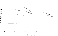
Fig. 7 is the figure of the relation between the light receiving element charging performance when showing about Eg value different in the Eu in the second layer zone of the photoconductive layer of light receiving element of the present invention and the second layer zone;
Fig. 8 is the figure that shows about the relation between the light receiving element temperature characterisitic during different Eg value in the Eu in the second layer zone of the photoconductive layer of light receiving element of the present invention and the second layer zone;
Fig. 9 one shows the figure about the relation between the light receiving element Exposure memory (light memory) during different Eg value in the Eu in the second layer zone of the photoconductive layer of light receiving element of the present invention and the second layer zone.
Describe below the present invention in detail.
In this explanation, characterize " non-crystalline material that is mainly consisted of by silicon atom " of non-monocrystalline silicon Often be called " amorphous silicon material ", to " mainly being consisted of by silicon atom and contain at least a The non-crystalline material of hydrogen atom and halogen atom " often be called " a-Si:X ". Noun " contains hydrogen The non-crystalline silicon of atom " also often be referred to as " amorphous silicon hydride ", and " the amorphous that contains halogen atom Silicon " be called " halogenation non-crystalline silicon ", these include in expression formula " a-Si:X ".
Light receiving element of the present invention comprises that one mainly consists of with silicon atom and to contain at least a hydrogen former The photoconductive layer that amorphous (on-monocrystalline) material of son and halogen atom forms. This photoconductive layer has Ground floor zone and a second layer of each own specific light band gap (Eg) and characteristic energy (Eu) The zone.
Photoconductive layer must contain hydrogen atom or halogen atom. It may not only contain hydrogen atom but also contain Halogen atom. This is so that the quality, particularly improvement that can compensate the dangling bonds of silicon atom and improve layer Photoconduction and charge holding performance.
In light receiving element, hydrogen atom and/or halogen atom composition (Ch) are in the ground floor zone In preferably may by 10 atom % (percentage) to the scope of 30 atom % (percentage), And in second layer zone, be preferably by 20 atom % to 40 atom %, as long as in the ground floor zone Ch less than the Ch in second layer zone. Be more preferably, Ch can be not little in the ground floor zone In in 15 atom % to the scope less than 25 atom %, and in second layer zone, can be not less than 25 atom % are to the scope that is not more than 35 atom %.
At this, noun " hydrogen atom and/or halogen atom composition (Ch) " is photoconductive when forming When layer only adds in the situation of hydrogen atom and refers to " hydrogen atom composition ", perhaps in that only to add halogen former Refer in the situation of son " halogen atom composition ", or in the feelings that add hydrogen atom and halogen atom Refer under the condition " summation of hydrogen atom composition and halogen atom composition ". Unit " atom % " be one with The ratio of total composition of hydrogen atom and/or halogen atom and silicon atom.
Photoconductive layer among the present invention must have one by 1.70eV extremely in the ground floor interval 1.82eV optical band gap (Eg) and in second layer zone by the optical band gap of 1.78eV to 1.85, As long as the Eg in ground floor zone is less than the Eg in second layer zone. Be more preferably, photoconductive layer can Have in the ground floor zone and be not less than 1.75eV extremely less than the Eg of 1.80eV with in second layer zone Be not less than 1.80eV to the Eg that is not more than 1.83eV.
Photoconductive layer in the present invention also must have a characteristic energy (Eu) that is obtained by the linear relationship part (exponential curve tail) with the function of formula (I) expression:
lnα=(1/Eu)·hγ+α
1 (I)
In the formula, photon energy (h γ) is set to an independent variable, and the suction of light absorption frequency spectrum Receiving coefficient (α) then is a correlated variables. This characteristic energy Eu is by 50meV in the ground floor zone Be by 50meV to 60meV to 65meV with in second layer zone, as long as the ground floor zone Eu is greater than the Eu in second layer zone; Be preferably in the ground floor zone is to being not more than greater than 55meV 65meV and in second layer zone, be not less than 50meV to being not more than 55meV.
Fig. 1 shows an example of the subband crack light absorption frequency spectrum of photoconductive layer among the present invention. Photon energy (h γ) by the paintings abscissa, the logarithm of the absorption coefficient of light absorption frequency spectrum (α) (ln α) By the paintings ordinate. This frequency spectrum can be divided into two parts roughly. One of them is the B part, The absorption coefficient here (α) relatively photon energy (h γ) is done index variation, and namely ln α is relative H γ makes linear change (this part is called " exponential curve tail " or " Urback tail "), another Individual is part A, and ln α shows as slighter changing with h γ here.
The light absorption that the B part that ln α makes linear change causes corresponding to the tail energy level of reason valence band side to the light transition of conduction band, absorption coefficient (α) is then represented by following formula (II) the dependence of photon energy (h γ):
α=α
0exp(hγ)/Eu (II)
α in the formula0Specific constant for photoconductive layer. The logarithm on modus ponens (II) both sides just obtains State formula (I).
lnα=(1/Eu)·hγ+α
1 (I)
α in the formula1Be ln α0。
In formula (I), the inverse (1/Eu) of characteristic energy (Eu) indicates the gradient of B part among Fig. 1.Eu is corresponding to the characteristic energy of the index energy distribution of tail energy level on the valence band side, and therefore less Eu shows the less tail energy level on the valence band side.
Light absorption frequency spectrum in subband crack is measured with deep level spectroscopic methodology, isothermal over capacity spectroscopic methodology, photo-thermal polarized light spectrometry, optoacoustic Spectrum Method or constant light current method usually.Particularly constant light current method (afterwards being called " CPM ") of great use.
In the present invention, the thickness of photoconductive layer is considering that aspects such as electrostatic printing performance, economic benefit determine rightly in addition.Its thickness can be preferentially to get between 20 μ m to the 50 μ m, more preferably between 23 μ m to 45 μ m, by preferably then between 25 μ m to 40 μ m.If thickness is less than 20 μ m, electrostatic printing performance (for example charging performance and sensitivity) may be just not enough in practicality.If it is greater than 50 μ m, then forming photoconductive layer just may need the long period, thereby increases production cost.
Such thickness can be preferentially got in the second layer zone of photoconductive layer, makes that promptly the ratio of thickness (thickness in ground floor zone adds the thickness in second layer zone) and the thickness in second layer zone of overall optical conductance layer is 1: 0.003 to 1: 0.15.If the ratio of the thickness of this 2nd layer region is less than 0.003, electric charge injects barrier properties just may be become inappropriate.Especially when second layer zone is placed in the top layer side, long wavelength's composition of pre-exposure and the exposure of visual formula just may not finely be absorbed, thereby makes that the temperature dependency and the Exposure memory of charging performance just can not reduce effectively in some situation.If it is greater than 0.15 on the other hand, in order to obtain the satisfied film quality in second layer zone, just must be formed, thereby will be formed photoconductive layer, thereby production cost is increased with the long period at the deposition speed that is lower than ground floor zone under the existing environment slightly.
The layer topology example (transversal section) of photoconductive layer among Fig. 2 A-2C explanation the present invention.Photoconductive layer 11 among Fig. 2 A has ground floor zone and second layer zone, and the group structure of layer is a second layer regional 2a is formed on the ground floor zone 1 with being applied.Photoconductive layer 11 among Fig. 2 B has a ground floor zone and a second layer zone, and its layer group structure to be ground floor zone 1 be formed on the regional 2b of a second layer with being applied.Photoconductive layer 11 among Fig. 2 c has ground floor zone and two second layer zones, and its layer group structure is that second layer zone 2a then superimposed landform becomes on ground floor zone 1 on the 2b of 1 superimposed landform Cheng Zaiyi second layer zone, ground floor zone.Label 10 refers to a base lining.
Thereby lowering the temperature dependency and the Exposure memory of charging performance, the group structure of using above-mentioned layer can reach purpose of the present invention.The group structure of the layer shown in the application drawing 2B makes can also obtain coarse visual aspect except that above-mentioned effect and improves (the entity image is checked CONCENTRATION DISTRIBUTION as image characteristics).The layer that photoconductive layer shown in Fig. 2 C not only has the layer group structure among Fig. 2 A but also has among Fig. 2 B is organized structure, therefore similarly also can obtain improvement on coarse image except that above-mentioned effect.
Photoconductive layer among the present invention is formed by the film vacuum deposition.Specifically, it can form by various thin film deposition process, as an example comprise AC discharge CVD as glow discharge, for example low frequency CVD, high frequency CVD or microwave CVD and DC discharge; And sputter, the deposited plating of vacuum metal, ion diffusion coating, optical cvd and hot CVD.When adopting these thin-film depositions to handle, according to create conditions, burden degree to capital investment in the equipment, production scale and the desired characteristic of light receiving element made and performance are selected suitable a kind of.Glow discharge, the high frequency glow discharge of particularly adopting RF band or VHF frequency range supply frequency is owing to it is easier to be paid the utmost attention to relative the saying of control processing conditions.
When forming photoconductive layer by glow discharge, basically be can be with the unstrpped gas (initial gas) that can supply with silicon atom (Si), the unstrpped gas that can supply with halogen atom with the unstrpped gas and/or one that can supply with hydrogen atom imports into desired gaseous state one can be pumped in the reactor of vacuum, and can make and in this reactor glow discharge takes place so that form photoconductive layer on the base lining that sets in advance on the given position.
The raw material that can supply with Si can comprise silane gaseous state or gasifiable, for example as SiH
4, Si
2H
6, Si
3H
8And Si
4H
10Deng silane, all can adopt effectively.The efficient of easiness of handling in the formation of consideration to layer and supply silicon preferably adopts SiH
4And Si
2H
6
For hydrogen atom being added photoconductive layer, mixed H in above-mentioned raw materials gas with ormal weight
2, H
2With the mixed gas of He or contain the silicon compound gas of hydrogen atom.This makes and is easy to control the ratio that adds hydrogen atom in the photoconductive layer.
The material that can supply with halogen atom preferably comprises halogen compounds gaseous state or gasifiable, and for example halogen gas, halogenide contain the halogen compounds of halogen and the silane derivative that replaces with a halogen.Material also can comprise the hydro-silicon compound that contains halogen gaseous state or gasifiable, and this also may be effective.Inter-halogen compounds can include fluorine gas (F especially
2), BrF, CIF, CIF
3, BrF
3, BrF
5, IF
3And IF
7The silicon compound that contains halogen atom, the promptly so-called silane derivative that substitutes with halogen atom can comprise silicon fluoride, as SiF
4And Si
2F
6
Above-mentioned raw materials gas can adopt separately, or with two or multiple form of mixtures use.
The hydrogen atom that adds in the photoconductive layer for control and/or the quantity of halogen atom are for example said the temperature of may command base lining, the quantity of material that is used to supply with hydrogen atom and/or halogen atom that is introduced into reactor, discharge power etc.For the parent material that adds above-mentioned atom can H when being employed
2Or He or H
2Mixed gas (diluents) dilution arbitrarily with He.
Photoconductive layer among the present invention preferably can be added in the atom that can control its electrical conductance when requiring.
The atom that can control electrical conductance must be comprised in the overall optical conductance layer but also make uniform CONCENTRATION DISTRIBUTION, but certain part can have nonhomogeneous density to distribute in the bed thickness direction.Even but when certain part has inhomogeneous CONCENTRATION DISTRIBUTION, for making the effect that adds them work equably, above-mentioned atom must comprise everywhere, and does the uniform concentration distribution on the in-plane parallel with base lining surface.
Can control the so-called impurity that is used for semiconductor applications that the atom of electrical conductance can comprise, and may utilize the atom (afterwards being called " IIIb of class family atom ") of the class family 13 that belongs to periodic table (3B of class family) that can give p type conduction, maybe can give the atom (back claims " Vb of class family atom ") of the class family 15 that belongs to periodic table (5B of class family) of type conduction.Wherein at least a atom is utilized.In other words, a kind of atom be can use separately, perhaps two kinds or more kinds of atom answered with form of mixtures.
The IIIb of class family atom can specifically comprise boron (B), aluminium (Al), gallium (Ga), indium (In) and thallium (Tl).Wherein B, Al and Ga are preferred.The Vb of class family atom can comprise phosphorus (P), arsenic (As), antimony (Sb) and bismuth (Bi).Wherein P and As are preferential.
The atom that can control its electrical conductance can preferentially be decided to be 1 * 10 at the content of photoconductive layer
-2Atom ppm to 1 * 10
2Atom ppm, more desirable is by 5 * 10
-2Atom ppm to 50 atom ppm and being more preferably by 1 * 10
-1Atom ppm to 1 * 10 atom ppm.Also wish to make composition second layer zone greater than the ground floor zone in.
Atom for the control of binding energy structurally electrical conductance can will be used to add the initiation material that can control electrical conductance when cambium layer, with gaseous state together with other gas that is used to form photoconductive layer (as mentioned above) feed-in reactor simultaneously.
These can be used as adding can control the parent material of the atom of electrical conductance should be selected from those under normal temperature and normal pressure for gaseous state or those under layer formation condition, be easy to vaporized material at least.This parent material that is used to add the IIIb of class family atom can comprise a boron hydride such as a B as the material that adds the boron atom
2H
6, B
4H
10, B
5H
9, B
5H
11, B
6H
10, B
6H
12And B
6H
14, and halogenation boron, for example BF
3, BCl
3And BBr
3In addition, material also can comprise AlCl
3, GaCl
3, Ga (CH
3)
3, InCl
3And TlCl
3For can comprising conduct, the parent material that adds the class Vb of family atom adds the hydrogenation phosphorus such as the PH of the material of phosphorus atoms
3And P
2H
4, and phosphorus Halides such as PH
4I, PF
3, PF
5, PCl
3, PCl
5, PBr
3, PBr
5And PI
3In addition, the material that can be effectively utilized also comprises AsH
3, AsF
3, AsCl
3, AsBr
3, AsF
5, SbH
3, SbF
3, SbF
5, SbCl
3, SbCl
5, BiH
3, BiCl
3And BiBr
3
These parent materials that are used to add the atom that can control electrical conductance can be with H when being employed
2Or He, or H
2Arbitrarily dilute with the mixed gas (diluents) of He.
In the present invention, it also is effective adding at least a boron atom, oxygen atom and nitrogen-atoms in photoconductive layer.These atoms on content preferably by 1 * 10
-5Atom % to 10 atom % is preferably by 1 * 10
-4Atom % to 8 atom % and more superior be by 1 atom % * 10
-3To 5 atom %, totally by the basis that adds up to of the silicon atom in the photoconductive layer, carbon atom, oxygen atom and nitrogen-atoms.
These carbon atoms, oxygen atom and nitrogen-atoms must be comprised in also must be made concentration and evenly distribute in the overall optical conductance layer, but certain part can have CONCENTRATION DISTRIBUTION heterogeneous in the bed thickness direction.But, even when some part has inhomogeneous CONCENTRATION DISTRIBUTION, for the adding that makes them plays useful effect equably, above-mentioned atom must contain everywhere, is not serving as a contrast on the parallel in-plane with uniform CONCENTRATION DISTRIBUTION with base.
The material that can supply with carbon atom as effective material can comprise hydrocarbon gaseous state or gasifiable, as CH
4, C
2H
2, C
2H
6, C
3H
8And C
4H
10Consider easiness and the feedback C efficient handled when cambium layer, material preferably comprises CH
4, C
2H
2And C
2H
6These unstrpped gases that can supply with carbon atom can be at them with gas H for example
2, optionally utilize after He, Ar or the Ne dilution.
The material that can supply with nitrogen or oxygen can comprise gaseous state or gasifiable compound, for example NH
3, NO, N
2O, NO
2, O
2, CO, CO
2And N
2The unstrpped gas of these feedback nitrogen or oxygen can be at them with gas H for example
2, He, Ar or Ne dilution back arbitrarily uses.
In order to realize purpose of the present invention, formation has the photoconductive layer of desired film characteristics, the unstripped gas that to supply with Si be must set rightly on request and blending ratio, the air pressure of inside reactor, discharge power and the base lining temperature of (back claims " feedback Si gas ") and diluents stopped.
Arbitrarily be used as the H of diluents
2Or He, or H
2Can suitably in an ideal range, select with the flowing velocity of the mixed gas of He according to the design of photoconductive layer group structure, and this diluents can be presented Si gas and be the basis, usually in by 3 to 20 times scope, be carried out mixing, preferably by 4 to 15 times, better by 5 to 10 times.
The air pressure of inside reactor also can be organized design suitably selection in an ideal range of structure according to layer.This pressure can be by 1 * 10 in common scope
-4Torr to 10Torr (1.333 * 10
-2Pa to 1.333 * 10
3Pa), preferably by 5 * 10
-4Torr to 5Torr (6.665 * 10
-2Pa to 6.665 * 10
2Pa), and better by 1 * 10
-3Torr to 1Torr (1.333 * 10
-1Pa to 1.333 * 10
2Pa).
Discharge power also can be organized design suitably selection in an ideal range of structure according to layer, and discharge power can preferentially be arranged on by in 3 to 8 the scope with the ratio (W/SCCM) of feedback Si gas flow speed for this reason, and better is by 4 to 6.In addition, discharge power preferably can be provided with greater than the ratio in the formation in ground floor zone with the ratio of the flow velocity of feedback Si gas in the formation in second layer zone, and forms in so-called circulation limit area.
The temperature of base lining can be set at usually by 200 ℃ to 350 ℃, and comparatively ideal is by 230 ℃ to 330 ℃, and is by 250 ℃ to 300 ℃ better.
The optimum condition scope of the mixing ratio of above-mentioned feedback Si gas and diluents, reactor internal pressure, discharge power and base lining temperature can not be separated definite isolatedly.Ideal conditions is suitable for determining so that can form the light receiving element that has the performance that requires with relation system according to mutual.
The base that adopted among the present invention lining can be that conductor base lining or is served as a contrast through the base that the insulating material of conductive processing constitutes in a side that forms photoconductive layer at least by its surface, and both all can adopt.Conductor base lining can comprise what those were made of metal, as Al, and Cr, Mo, Au, In, Nb, Te, V, Ti, Pt, Pd or Fe or their any alloy, for example stainless steel.Be subjected to the insulating material of conductive processing can comprise film of synthetic resin or sheet as basic laying-in, for example polyester, PEF, polycarbonate, cellulose acetate, polypropylene, Polyvinylchloride, polystyrene or acid amides, or glass or pottery.
Base lining used among the present invention can have band smooth surfaces or the cylinder on out-of-flatness surface or the shape of sheet Endless belt.The thickness of base lining can suitably be determined on request.Requiring to have in the situation of dirigibility as an electrostatic printing light receiving element, this base lining is as long as it can be as it being done thin as much as possible once the good operation of base lining.But under normal conditions, consider its processing and processing, physical strength or the like, basic lining may have thickness 10 μ m or bigger.
When adopting interference light (for example laser) recording picture, the surface of the base lining that adopts among the present invention can be made to irregular, may eliminate any image inferior that causes because of the so-called interference fringe that occurs in the visual image by this effectively.The irregularity degree that makes on the surface of base lining can adopt known method to produce, as disclosing among Japanese Patent Application Publication No.60-168156, No.60-178457 and the No.60-225854.
As making the another kind of method of surface irregularity, be the male and fomale(M﹠F) of on base lining surface, making many tracks spherical in shape.In the out-of-flatness that forms like this, the irregularity degree that the surface of base lining has is trickle than the required resolution of light receiving element.The out-of-flatness of Xing Chenging can adopt the known method that is disclosed among the Japanese Patent Application Publication No.61-231561 to produce like this.
Best superimposed landform becomes a top layer on the photoconductive layer of light receiving element of the present invention, and it is formed by a main at least a non-crystalline material that be made of silicon atom and that contain in carbon atom, oxygen atom and the nitrogen-atoms.
These carbon atoms, oxygen atom and nitrogen-atoms must be comprised in the overall optical conductance layer, and do the uniform concentration distribution, but in some part of layer thickness direction non-homogeneous CONCENTRATION DISTRIBUTION can be arranged.But even the inhomogeneous CONCENTRATION DISTRIBUTION of certain part is arranged, for the effect that their are added realizes that equably above-mentioned atom must all comprise everywhere, and on the in-plane parallel, make uniform concentration and distribute with base lining surface.
Fig. 3 explanation has the layer group structure example (cross-sectional view) of the light receiving element on this top layer.One photoconductive layer 11 is superimposed on the surface of base lining 10, and a top layer 12 is formed on this photoconductive layer with being applied.In example as shown in Figure 3, photoconductive layer 11 has ground floor zone 1 and becomes into second layer zone 2a (being similar to Fig. 2 A) on the ground floor zone with a superimposed landform.In other words, it can have the layer group structure as shown in Fig. 2 B or Fig. 2 C.
When forming this top layer among the present invention, it forms thickness can preferentially be by 0.01 μ m to 3 μ m, is by 0.05 μ m to 2 μ m preferably, and is more preferably by 0.1 μ m to 1 μ m.If layer thickness is less than 0.01 μ m, this top layer can be because of the very fast losses such as friction during the light receiving element application.If the electrostatic printing performance that the increase of residual electric potential for example etc. greater than 3 μ m, then can take place for it reduces.
Have a Free Surface as above-mentioned top layer, be made to so that improve moisture resistance, continuous repeat performance, electric breakdown strength, running environment characteristic and operating performance.As photoconductive layer, this top layer utilizes non-single-crystal material to form, particularly a kind of non-crystalline material that mainly constitutes by silicon atom, and on the interface between the overlapping layer, guarantee good chemistry and structural stability thus.
Top layer of the present invention can adopt any material to form, as long as they are non-single crystal silicon materials, and the particularly main non-crystalline material (being amorphous silicon material) that constitutes by silicon atom.For example, preferably adopt a kind of hydrogen atom and/or halogen atom (amorphous silicon material of back title " a-Si:X " of containing.In addition, be more preferably employing one and contain a-Si:X at least a in carbon atom, oxygen atom and the nitrogen-atoms.Especially an a-Si:X who contains carbon atom is best.When the a-Si:X that uses carbon atoms forms when forming this top layer as main, within the scope of 30 atom % to the 90 atom % that the carbon content in the top layer can be preferentially be benchmark with the sum and the carbon number of silicon atom.
Top layer among the present invention requires to comprise hydrogen atom or halogen atom.Also can contain hydrogen atom and halogen atom.When adding hydrogen atom, be suitable for to hydrogen atom control so that with composed atom add up to its content of benchmark for by 30 atom % to 70 atom %, be preferably by 35 atom % to 65 atom %, be more preferably by 40 atom % to 60 atom %.When adding halogen atom, be suitable for halogen atom is controlled so that add up to its content of benchmark for by 0.01 atom % to 15 atom % with composed atom, preferentially be by 0.1 atom % to 10 atom %, be more preferably by 0.6 atom % to 4 atom %.
Control their the feasible quality that may compensate the unsettled chain of silicon atom and improve layer of composition like this, particularly improve photoconductive property and charge holding performance.
The light receiving element that is used for electrostatic printing has problem as described below.For example, charging performance may inject because of the electric charge from Free Surface and worsen; Charging performance may be because of in a running environment, for example in high humidity environment, and the variation of surface structure and changing; And during at corona discharge or with rayed electric charge by photoconductive layer iunjected charge top layer may be because of the defective of inside, top layer in remaining imaging (after-image) phenomenon of trap-charge during causing repeated application.These are that known any defective or imperfection (dangling bonds that is mainly silicon atom or carbon atom causes) by the inner existence in top layer caused.
Make the defective in the top layer reduce greatly but in the top layer, add hydrogen atom and hydrogen atom content in the top layer is controlled to 30 atom % to 70 atom %, thereby can on electric characteristics and high-speed and continuous application performance, improve.If hydrogen atom less than 30 atom %, just can't reach above-mentioned effect in some cases on content.If but hydrogen atom content is greater than 70 atom % on the other hand, the hardness on top layer may reduce, thereby this layer then can't bear repeated application in some cases.Hydrogen atom content can be controlled when the processing and manufacturing described later according to the flow velocity of unstrpped gas and ratio, base lining temperature, discharge power, air pressure etc. in the top layer.
In the top layer, add halogen atom and halogen atom in the top layer is controlled to its content and more effectively realize forming of the key between silicon atom and carbon atom in the top layer for making by 0.01 atom % to 15 atom %.And the halogen atom in the top layer can also prevent the fracture that the key between silicon atom and carbon atom causes because of corona discharge etc. effectively.If halogen atom is lower than 0.01 atom % or greater than 15 atom %, just can not reaches above-mentioned effect in some cases on content.When halogen atom on content greater than 15 atom %, because moving of charge carrier and may make residual electric potential and iconic memory become fairly obvious in the excessive halogen atom overslaugh top layer.Halogen atom content can be controlled according to velocity of liquid assets and ratio, basic temperature, discharge power, the gaseous tension etc. of serving as a contrast of unstrpped gas as the control to hydrogen atom content in the top layer.
Top layer among the present invention can form with the same mode of aforesaid formation photoconductive layer.For example, when relying on glow discharge to form the top layer of forming by an a-Si:X who contains carbon atom, usually the unstrpped gas that the unstrpped gas and/or one that the unstrpped gas and one that the unstrpped gas, one that can supply with silicon atom can be able to be supplied with carbon atom can be supplied with hydrogen atom can be supplied with halogen atom is introduced the reactor that its inside into can be made to vacuum with desired gaseous state, and make glow discharge takes place, thereby form the top layer setting in advance on the photoconductive layer on the lining of the base on the certain position in reactor.
These can be supplied with in the raw material of silicon atom, carbon atom, oxygen atom and nitrogen-atoms in the situation with photoconductive layer is identical.As the material that can supply with hydrogen atom, can adopt H
2Gas, H
2Mixed gas or a kind of silicon compound gas that contains hydrogen atom with He.These unstrpped gases are mixed with other gases with aequum in application.This feasible additional proportion of more easily controlling the hydrogen atom in the top layer.As the material that can supply with halogen atom, can adopt with photoconductive layer in used same material.Above-mentioned raw materials gas can be used separately separately, perhaps is applied with two kinds or multiple form of mixing mutually.
In order to control the hydrogen atom that is added into the top layer and/or the amount of halogen atom, can control with identical mode under the photoconductive layer situation.
Top layer among the present invention as aforesaid photoconductive layer, preferably can be added into can control the atom of its electric conductivity.
This atom that can control electric conductivity must be comprised in the whole top layer and make uniform concentration and distribute, but in some part of layer thickness direction uneven CONCENTRATION DISTRIBUTION can be arranged.Even but in some part inhomogeneous CONCENTRATION DISTRIBUTION is arranged, for the effect that they are added works equably, above-mentioned atom must comprise everywhere and make uniform CONCENTRATION DISTRIBUTION on the in-plane parallel with base lining surface.
Can control amount that the atom of electric conductivity contained preferably by 1 * 10 in the top layer
-3Atom ppm to 1 * 10
3Atom ppm is by 1 * 10 preferably
-2Atom ppm to 5 * 10
2Atom ppm, and be more preferably by 1 * 10
-1Atom ppm to 1 * 10
2Atom ppm.
Can control the kind of the atom of electric conductivity, its parent material, as the state that atom added the top layer all can with aforementioned lights conductance layer situation in identical.
For realizing that purpose of the present invention forms the top layer with the film characteristics that requires, the blending ratio of feedback Si gas and diluents, air pressure, discharge power and the base lining temperature of inside reactor suitably must be provided with on request.About the air pressure of inside reactor and base lining temperature, they can be set with same mode in the photoconductive layer situation.
Thereby the top layer that forms in the above described manner among the present invention is made subtly and can be endowed required performance according to hope.More specifically say on the structure viewpoint, to have at least a and hydrogen atom in silicon atom, carbon atom, oxygen atom and the nitrogen-atoms and/or halogen atom top layer, depend on that the condition when it forms presents by the form of crystallization to amorphous as its composition.Viewpoint by electrical specification sees, it shows by conductor to the character of semiconductor until mutual insulation, and by photoconduction to non-photoconductive character.Thereby correspondingly, the condition of its formation is carried out strict selection so that can form the top layer with the characteristic that requires.For example saying, mainly is being when being used to improve the purpose of its disruptive strength when this top layer, and this top layer just is formed the amorphous form with significant electrical insulation properties in running environment.When the top layer mainly is to be for improving the purpose that repeats due performance and running environment characteristic continuously, it just is formed grade with its above-mentioned electrical insulative property and is reduced to a certain degree and have a amorphous form to certain sensitivity of the light that shines this layer.
Light receiving element of the present invention can have one between photoconductive layer and top layer to have than top layer content be the restraining barrier (lower top layer) of few carbon atom, oxygen atom and nitrogen-atoms.This make can as performance such as charging on bigger improvement.
The adjacent domain at the interface in the top layer between top layer and photoconductive layer can be provided with a zone, and wherein the content of carbon atom, oxygen atom and nitrogen-atoms reduces towards photoconductive layer.This make may improve adhesion between top layer and photoconductive layer, smoothly to the mobile photocarrier in surface with reduce the fixing interference that causes because of the reflected light at the interface between photoconductive layer and surface more.
In light receiving element of the present invention, preferably make an electric charge inject the atom that the restraining barrier is mainly constituted and included at least a of carbon atom, oxygen atom and nitrogen-atoms and can control electric conductivity by silicon atom, and the photoconductive layer superimposed landform is become on this electric charge injection restraining barrier.More specifically, when between the base lining of conduction and photoconductive layer, making when playing the electric charge that prevents by the function of conduction base lining side iunjected charge and injecting the restraining barrier, just make more effectively to reach purpose of the present invention.In this case, just whether unqualified to the existence on top layer.More preferably, can on photoconductive layer, become the top layer by superimposed landform.
Fig. 4 explanation (cross-sectional view) has the example of layer group structure that electric charge injects the light receiving element on restraining barrier and top layer.One electric charge injection restraining barrier 13 is superimposed on the surface of a base lining 10, and a photoconductive layer 11 is formed on the electric charge injection restraining barrier 13 with being applied and a top layer 12 is formed on this photoconductive layer with being applied.In example shown in Figure 4, photoconductive layer 11 has the second area 2a (identical with Fig. 2 A) that ground floor zone 1 and a superimposed landform become thereon.On the other hand, the layer that can have as shown in Fig. 2 B or Fig. 2 C is organized structure.
Electric charge injects the restraining barrier and can preferentially get it to form thickness be 0.1 μ m to 5 μ m among the present invention, preferably can be by 0.3 μ m to 4 μ m, and better desirable by 0.5 μ m to 3 μ m.If layer thickness is less than 0.1 μ m, the effect that electric charge injects the restraining barrier possibly can't realize in some cases.If it is greater than 5 μ m on the other hand, just can not reach by making this thickness increase desired any desired improvement the electrostatic printing performance, also may cause production cost to increase because be used to form the time lengthening of film.
Electric charge injects the restraining barrier have the effect that prevents by base lining lateral light conductance layer iunjected charge when light receiving element charges with a certain polarity among the present invention, then is revealed as no such effect when charging with opposite polarity, and this is referred to as the polarity dependence.
In order to give this function, must inject the restraining barrier at electric charge and add the atom that to control its electric conductivity.When also this atom adding that can control electric conductivity being gone into photoconductive layer, the content that they inject the restraining barrier at electric charge must quilt be done greater than the content of photoconductive layer.
This atom that can control electric conductivity must be comprised in whole electric charge and inject the restraining barrier and make uniform CONCENTRATION DISTRIBUTION, but can uneven CONCENTRATION DISTRIBUTION be arranged in certain part in the bed thickness direction.The uneven part of this CONCENTRATION DISTRIBUTION preferably can be the more base lining side that is distributed in.Even but when certain part had uneven CONCENTRATION DISTRIBUTION, for the adding effect that makes them works equably, above-mentioned atom must comprise everywhere and make uniform CONCENTRATION DISTRIBUTION on the in-plane that is parallel to base lining surface.
The content of atom in the top layer that can control electric conductivity is preferably by 10 atom ppm to 1 * 10
4Atom ppm is preferably by 50 atom ppm to 5 * 10
3Atom ppm, and more preferably by 1 * 10
2Atom ppm to 3 * 10
3Atom ppm.
Can control the kind, its parent material of the atom of electric conductivity and atom and add identical that mode that electric charge injects the restraining barrier all can be with the situation of aforementioned lights conductance layer.
In the present invention, it also is effective adding at least a of carbon atom, oxygen atom and nitrogen-atoms on electric charge injection restraining barrier.These atoms are that benchmark is preferably got by 1 * 10 totally by the summation that electric charge injects silicon atom, carbon atom, oxygen atom and the nitrogen-atoms on restraining barrier on content
-3Atom % to 30 atom % is preferably by 5 * 10
-3%20 atom %, and desirable better by 1 * 10
-2Atom % to 10 atom %.
These carbon atoms, oxygen atom and nitrogen-atoms must be comprised in whole electric charge injection resistance works as layer and makes uniform CONCENTRATION DISTRIBUTION, but in layer thickness direction part uneven CONCENTRATION DISTRIBUTION can be arranged.But, even when certain part has inhomogeneous CONCENTRATION DISTRIBUTION, for the effect that they are added works equably, above-mentioned atom must contain everywhere, and makes uniform CONCENTRATION DISTRIBUTION on the in-plane that is parallel to base lining surface.
At least a feasible can the improvement better with other that adds by this way in carbon atom, oxygen atom and the nitrogen-atoms is made to the adhesion that injects the contacted layer in restraining barrier with electric charge.
Electric charge injects the restraining barrier and can adopt a non-crystalline material (amorphous silicon material) that mainly is made of silicon atom optionally to comprise above-mentioned atom to form among the present invention.As this amorphous silicon material, preferably adopt the amorphous silicon material that contains hydrogen atom and/or halogen atom (a-Si:X).Hydrogen atom in this layer and/or halogen atom have same effect in the situation with aforesaid photoconductive layer and top layer.
The hydrogen atom on electric charge injection restraining barrier and/or the content of halogen atom are preferably desirable 1 atom % to the 50 atom % of benchmark with the summation of silicon atom and hydrogen atom and/or halogen atom, desirable preferably 5 atom % to 40 atom %, and get 10 atom % to 30 atom % better.
Can supply with silicon atom, carbon atom, oxygen atom and nitrogen-atoms material can with the photoconductive layer situation in identical.Can adopt H as the material that can supply with hydrogen atom
2Gas, H
2Mixed gas or a kind of silicon compound gas that contains hydrogen atom with He.These unstrpped gases are mixed with other gas by required amount when using.This makes easier control electric charge inject the ratio that the restraining barrier adds hydrogen atom.As the material that can supply with halogen atom can adopt with photoconductive layer in used identical materials.Above-mentioned material can be used separately separately, also can two kinds or more kinds of mixed forms be applied.
Among the present invention electric charge inject the restraining barrier by aforesaid film vacuum deposition technique with form photoconductive layer the same manner and form.
Inject the restraining barrier in order to form the electric charge of realizing the object of the invention, must suitably set the mixing ratio of feedback Si gas and diluents, air pressure, discharge power and the base lining temperature of inside reactor on request with the film characteristics that requires.For discharge power, this discharge power is suitable for being set in by in 0.5 to 8 the scope with the ratio of the velocity of liquid assets of feedback Si gas, is by 0.8 to 7 preferably, more preferably by 1 to 6.The mixing ratio of feedback Si gas and diluents, the air pressure of inside reactor and base lining temperature can be by being provided with photoconductive layer situation the same manner.
In according to the photoconductive layer of light receiving element of the present invention aluminium atom, silicon atom and hydrogen atom and/or halogen atom preferably can the layer thickness direction do uneven distribution (that is, in base lining side mainly by the aluminium atomic building and become mainly towards the surface gradually constitute by silicon atom).What this brought between base lining and the photoconductive layer adhesion condition at the interface improves (particularly electric charge injection restraining barrier) so that be difficult to take place trickle peeling off with cracked, and gradually changing of composition make charge carrier can be reposefully be flowed to the base lining by photoconductive layer, and the result improves image quality.
Also can between base lining and photoconductive layer, an adhesion layer be set, perhaps when being provided with electric charge and injecting the restraining barrier, inject between restraining barrier and basic the lining in addition this adhesion layer at this electric charge.This adhesion layer further improves the adhewsive action to the base lining.This adhesion layer is for example by Si
3N
4, SiO
2, at least a non-crystalline material that contains in hydrogen atom and/or halogen atom and carbon atom, oxygen atom and the nitrogen-atoms that mainly is made of silicon atom of SiO or forms.
Between base lining and photoconductive layer, perhaps when being provided with electric charge injection restraining barrier, inject between restraining barrier and the base lining at electric charge, a light absorbing zone (for example IR absorption layer) also can be set.This light absorbing zone prevents the generation by the caused interference fringe of light of base lining reflection.
To describe in detail below according to the present invention and form the equipment of electrostatic printing light receiving element and the film forming method that this equipment of employing forms above-mentioned each layer.
Fig. 5 illustrates utilization with the device examples (back claim " RF-PCVD ") of RF band as the high frequency plasma promotion CVD manufacturing light receiving element of supply frequency, and this is a kind of glow discharge.Process equipment shown in Fig. 5 is by following formation.
This process equipment mainly is made up of a deposition system 5100, the unstrpped gas evacuation system (not shown) that system 5200 and is used for abstraction reaction device 5101 inner vacuum of feeding.Be provided with cylindrical base lining 5102, one a base lining well heater 5103 and the unstrpped gas pipe 5104 of feeding in the reactor 5101 in deposition system 5100.One high frequency matching box 5105 also is connected to reactor.
This cylindrical basic lining can adopt any measure heating, as long as it has the heater block of vacuum type.A kind ofly like this can include electric resistance heater (for example an encapsulation heating head coiling property well heater, plane heater and ceramic heater), heat radiation tube heater block (for example halide torch and infrared tube) specially and with a heating element that adopts liquid, gas etc. to constitute for the well heater that adds hot radical lining as the heat-exchange device of thermal medium.As the surfacing of heating arrangement, can adopt the metal that resembles stainless steel, nickel, aluminium and copper etc., pottery, solar heat protection polymer resin etc.Another kind method is, adds a container that is exclusively used in heating outside reactor, after basic lining can heat therein and be transported in the reactor.Can adopt such method.
Layered material gas is fed system 5200 by gas tank 5201-5206, and with the pressure controller 5251-5256 of the corresponding setting of these gas tanks, pipeline valve 5211-5216,5221-5226 and 5237-5236, and mass flow controller 5241-5246 forms.The pipeline of unstrpped gas gas tank separately all is connected to feedback tracheae 5104 in the reactor 5101 via an auxiliary valve 5261 by unstrpped gas pipe 5106.
Utilizing the process equipment shown in Fig. 5 to form film by RF-PCVD can be undertaken by (for example) following method.
At first cylindrical base lining 5102 is inserted reactor 5101, and utilize an evacuator (not shown, for example a vacuum pump) that vacuum is extracted in reactor 5101 inside.Then, the well heater 5103 that is used to add the hot radical lining is controlled at predetermined temperature with the temperature of cylindrical base lining 5102, for example by 200 ℃ to 350 ℃.This temperature is suitable to be taken as 230 ℃ to 330 ℃, desirable better by 250 ℃ to 310 ℃.
Before the unstrpped gas that is used to form film flows to reactor 5101, the leak valve 5107 of inspection gas tank valve 5211~5216 and reactor is all closed to confirm them, also check to flow into valve 5221-5226 simultaneously, flow out valve 5231-5236 and one and help valve 5261 all to open to guarantee them.
Then, opening a main air release 5108 is evacuated with the inside with a reactor 5101 and a tracheae 5106.Reading at vacuum meter (G) 5109 is indicated as about 5 * 10
-6During the pressure of Torr, close auxiliary valve 5261 and flow out valve 5231-5236.
After this, open gas tank valve 5211-5216, and with on-stream pressure controller 5251-5256 each gas is controlled to and has about 2kg/cm so that respectively each gas is introduced into reactor 5101 by gas tank 5201-5206
2Pressure.Then open lentamente and flow into valve 5221-5226 so that respectively each gas is introduced matter stream controller 5241-5246.
Like this for begin to carry out film form ready after, just form each layer by following process.
When cylindrical base lining 5102 has reached a predetermined temperature, outflow valve 5231-5236 that some are necessary and auxiliary valve 5261 open lentamente make close predetermined gas by gas tank 5201-5206 by feedback tracheae 5104 feed-in reactors 5101.Then operate matter stream controller 5241-5246 so that adjust each unstrpped gas to such an extent that circulate at a predetermined velocity.Main air release 5108 is conditioned to such an extent that (observing vacuum meter 5109 simultaneously) makes reactor 5101 pressure inside reach the predetermined pressure that is not more than 1Torr in this process.
Reach when stablizing in this internal pressure, one has frequency for example for the RF power supply (not shown) of 13.56MHz is set to desired electric power, and it is inner so that glow discharge takes place by matching box 5105 the RF power supply to be supplied to reactor 5101.The discharge energy that is produced like this by the unstrpped gas of feed-in reactor decomposes, thereby forms the film that mainly is made of silicon on cylindrical base lining 5102.Behind the film that forms institute's required thickness (bed thickness), stop the supply of RF power supply, and close the outflow valve to stop the gas inflow reactor.So just finished the formation of film.
Repeat aforesaid operations for several times, just can form the electrostatic printing light receiving element that has desired sandwich construction by this.
When forming corresponding layer, the outflow valve except that the outflow valve that is used for desired gas all must Close All.And in order to prevent that corresponding gas residue from extending in the pipe of reactor 5101 at reactor 5101 with by flowing out valve 5231-5236, close and flow out valve 5231-5236, open auxiliary valve 5261 and then main air release 5108 is opened fully, so that internal system is pumped into high vacuum again; But this is an optional operation.
Being formed uniformly film in order to reach, is resultful by a driving mechanism (not shown) with this cylindrical base lining 5102 of predetermined speed rotation in the film forming while.
Self-evident, said process can be according to the formed condition change of each layer.
To introduce the process that promotes CVD (back claims " VHF-PCVD ") manufacturing electrostatic printing light receiving element with the VHF frequency range as the high frequency plasma of supply frequency that adopts below.
This process equipment is mainly by a deposition system (see figure 6), and the unstrpped gas system (among Fig. 5 5200) and of feeding forms as the evacuation system (not making among the figure) of the inside reactor of finding time.In the deposition system shown in Fig. 6, in a reactor 6101, be provided with cylindrical base lining 6102, base lining well heater 6103, unstrpped gas feed a pipe (not shown) and an electrode 6110.One matching box 6105 also is connected to this electrode.Reactor 6101 has a gas outlet 6111 and is connected with an evacuation system (not shown) by it.In reactor, form a discharge space 6112 by cylindrical base lining 6102 spaces that center on.Be provided with the base lining rotary electric machine (M) 6113 that is used to rotate this cylindrical base lining in the reactor outside.This cylindrical base lining by with the RF-PCVD situation in identical method heating.
As the unstrpped gas that the is connected to deposition system system of feeding, can adopt and the same system of system 5200 of feeding of the unstrpped gas shown in Fig. 5.
Utilizing this process equipment to form film by VHF-PCVD can carry out as follows.
At first, cylindrical base lining 6102 is placed reactor 6101.When cylindrical base lining 6102 is served as a contrast rotary electric machine 6113 driven rotary by base separately, inside reactor relies on an evacuator (not shown), for example a diffusion pump is pumped into vacuum by gas outlet 6111, controls reactor internal pressure to such an extent that for example be not more than 1 * 10
-7Torr.And then, the temperature of each cylindrical base lining remains on 200 ℃ to 350 ℃ of predetermined temperature with base lining well heater 6103 by heating.Preferably temperature is set in by 230 ℃ to 330 ℃, more preferably 250 ℃ to 310 ℃.
Then, with above-mentioned RF-PCVD situation under equal state carry out valve operation and exhaust, become unstrpped gas to present into reactor 6101 thin type.
Begin like this to form film ready after, according to following process for forming each rete.
When each cylindrical base lining 6102 arrived predetermined temperature, reactor 6101 was full of discharge space 6112 with gas so that present into by gas tank by the feedback tracheae said gas slowly to open some necessary outflow valves and auxiliary valve.Then operate the matter stream controller so that adjust each unstrpped gas mobile at a predetermined velocity.In this process, regulate main air release (monitoring vacuum meter simultaneously) and make discharge space 6112 pressure inside arrive the predetermined pressure that is not more than 1Torr.
Become when stablizing in internal pressure, for example will have that the VHF power supply (not shown) of the frequency of 500MHz is set at required electric power, and by a matching box 6105 a VHF power supply is provided to discharge space 6112 and makes glow discharges take place.Thereby in discharge space 6112, promptly encouraged and produce separation, consequently on each conduction base lining 6102, form required film by discharge energy by the unstrpped gas of feed.In this course, basic lining relies on base lining rotary electric machine 6113 to rotate with required rotating speed so that can the adequate relief film forming layer.Stop to supply with the VHF power supply after having the film of institute's required thickness forming one, and close and flow out valve to stop the gas inflow reactor.Thereby finished the formation of deposited film.
Aforesaid operations is repeated can form the electrostatic printing light receiving layer with desired sandwich construction by this for several times.
When forming corresponding layer, as the RF-PCVD situation, all except that the outflow valve of desired gas flow out valve all must close.And in order to prevent that corresponding gas from remaining in reactor and extend in the pipeline of reactor by flowing out valve, will flow out valve and close auxiliary valve is opened, then main air release is opened fully so that once more internal system is pumped into and be high vacuum; This can randomly operate.
Much less, said process can be according to the condition change of each layer formation.
Pressure among the VHF-PCVD in the discharge space preferably is set to by 1mTorr (1.333 * 10
-1Pa) to 500mTorr (6.665 * 10
1Pa), be by 3mTorr (3.999 * 10 preferably
-1Pa) to 300mTorr (3.999 * 10
1Pa), be and better by 5mTorr (6.665 * 10
-1Pa) to 100mTorr (1.333 * 10
1Pa).
In the process equipment that adopts VHF-PCVD, electrode set in the discharge space can have any size and shape, as long as it can not cause the discharge imbalance.At practical application, it preferably has the cylindrical shape of diameter by 1mm to 10cm.Here, the length of electrode also can arbitrarily be set, as long as its length is enough to make electric field to act on equably on the base lining.This electrode can unrestrictedly be made as long as conduct electricity on its surface by any material.For example, usually adopt such as metals such as stainless steel, Al, Cr, Mo, Au, In, Nb, Te, V, Ti, Pt, Pb and Fe, arbitrary their alloy, perhaps its surface with any above-mentioned work the glass or the pottery of conductive processing.
The inventor notices the performance of charge carrier in the photoconductive layer, and the CONCENTRATION DISTRIBUTION of the localization state of hydrogenation in the band gap and/or halogenation amorphous silicon and the relation between charging performance, its temperature dependency and the Exposure memory (light memory) have been made extensive studies.As a result of, relied on the thickness direction of photoconductive layer localization state CONCENTRATION DISTRIBUTION in the control band gap, that is control hydrogen atom and/or halogen atom content (Ch), optical band gap (Eg) and characteristic energy (Eu), and also rely on superimposed landform to become two kinds of layer regions to realize purpose of the present invention with these different values.
More specifically say, do the optical band gap of photoconductive layer big and do lessly to the speed of capturing of localization energy level charge carrier, can improve charging performance by this greatly and can reduce its temperature dependency simultaneously, and can also exempt the generation of Exposure memory basically.The generation that when adopting certain layer group structure, can also alleviate image of poor quality.
Above-mentioned these can be described in more detail as follows: in the band gap of hydrogenation and/or halogenation amorphous silicon, ubiquity has the incomplete deep level of structure of the dangling bonds of tail (end) energy level of structural imbalance of a cause Si-Si key and a cause Si etc.These energy levels are known, play a part to capture with the center in recombination electronics and hole to make the characteristic of device reduce.
Temperature dependent reason as charging performance, that is the reason that reduces at the charging performance that when with heating light activated elements such as cydariform well heaters, takes place, be considered to such: be subjected to heat activated charge carrier by the electric field leading that forms when the charging to the surface move repeat them simultaneously be the capturing and discharge of the localization energy level of magnetic tape trailer in the band gap and dark localization energy level, and eliminate surface charge subsequently.At this, charge carrier arrives the surface between charge period seldom influences charging performance, will eliminate surface charge and make charging performance reduce but the charge carrier of capturing in the deep level arrives the surface (after they pass charging unit) after the charging.Also being eliminated surface charge by the charge carrier of thermal excitation after the charging makes charging performance reduce.In order to prevent this point, also to improve the activity of charge carrier with regard to the generation that needs prevention thermal excitation charge carrier.
Thereby, do optical band gap to such an extent that prevent to produce the thermal excitation charge carrier more greatly, and capture the activity of the speed improvement charge carrier of charge carrier in the energy level that reduces to localize, just can prevent that with this charging performance from reducing.
As for Exposure memory (light memory), it also is that to be captured in the band gap localization energy level these charge carriers that neutralize at the photocarrier that is generated by the exposure of blank exposure or image-type caused when being retained in the photoconductive layer.More specifically, in the middle of the photocarrier that in a certain process of duplicating, produces, be retained in charge carrier in the photoconductive layer when the charging of following or the electric field that is formed by surface charge later on remove, be lower than other parts and become, thereby just on image, produce concentration difference at the current potential of the part that is exposed to light.For preventing this situation, the activity that must improve charge carrier is so that they can move through photoconductive layer and not allow photocarrier be retained in this one deck as far as possible in a duplicating process.
Like this, be provided with that Ch is wherein done greatly, Eg done big face and to Eu controlled (reductions) layer, stop the generation of thermal excitation charge carrier by this but also reduce the thermal excitation charge carrier or the ratio of the photocarrier that localization is captured in the energy level, thereby just can greatly improve the activity of charge carrier.
Below will be to narrate the present invention for example in more detail.The present invention also never is limited to these examples.
Example 1
Adopt the process equipment shown in Fig. 5 to make according to electrostatic printing light receiving element of the present invention by RF-PCVD.Become several retes going up superimposed landform once the aluminium cylinder (base lining) of the diameter 80mm of mirror grinding, it is that an electric charge injects restraining barrier, a photoconductive layer and a top layer in proper order, and they form under condition shown in the table 1.At this, photoconductive layer is formed a ground floor zone and a second layer zone, and they inject the restraining barrier side by electric charge in this order and begin to form with being applied.
It is 23 atom % that the ground floor zone of photoconductive layer has hydrogen richness (Ch), optical band gap (Eg) 1.77eV and characteristic energy (Eu) 60meV.It is 32 atom % that second layer zone has Ch, and Eg is that 1.83eV and Eu are 53meV.These results are the value by the resulting conduct of aftermentioned method " measurement of Ch, Eg and Eu ".
The performance of the light receiving element of Chan Shenging is assessed by the aftermentioned mode like this.As a result of, all obtaining good value aspect all charging performances, temperature characterisitic and the Exposure memory.On image, do not see Exposure memory yet.Spot both not having taken place blurred image had not taken place yet, only seen small image of poor quality, had shown that image characteristics was good.Particularly aspect charging performance, temperature dependency and Exposure memory, this light receiving element shows than the performance of the light receiving element with the photoconductive layer that only is formed with the ground floor zone better.
Table 1 gas species/condition electric charge injects the restraining barrier photoconductive layer
Second layer zone, ground floor zone top layer SiH
4(SCCM) 200 200 100 10H
2(SCCM) 300 1,000 800 0B
2H
6(ppm) 2,000 210 based on SiH
4NO (SCCM) 500 0CH
4(SCCM) 000 500 base lining temperature, (℃) 290 290 280 280 pressure, (Torr) 0.5 0.5 0.5 0.5 RF power, (W) 500 800 600 200 bed thickness, (μ m) 3 28 2 0.5
In this example, also with the same manner but in forming second layer zone, change SiH
4With H
2Mixing ratio, SiH
4Gas has been made the various light receiving element that has different Ch, Eg and Eu in the second layer zone with the ratio and the base lining temperature of discharge power.The thickness in ground floor zone and second layer zone is fixed as 28 μ m and 2 μ m respectively.
The performance of the variant light receiving element of Chan Shenging obtains the result shown in the difference among Fig. 7,8 and 9 through assessment like this.These Fig. 7,8 and 9 show about light receiving element of the present invention in the second layer zone of photoconductive layer during different Eg value, and the Eu in second layer zone respectively and the relation between the charging performance of light receiving element, temperature characterisitic and the Exposure memory.Charging performance, temperature characterisitic and memory current potential all show with relative value, and with the value of light receiving element with the photoconductive layer that only forms the ground floor zone as 1.Can know by these results and to see, the improvement that the light receiving element with the second layer zone that particularly has 1.8eV or above Eg and 55meV or following Eu all shows performance at charging performance, temperature characterisitic and Exposure memory aspect all.
Example 2
Except that ground floor zone with second layer zone becomes with the reversed sequence superimposed landform, produced according to electrostatic printing light receiving element of the present invention in the mode (under condition as shown in table 1) identical with example 1.
Assess the performance of the light receiving element of such generation in the aftermentioned mode.As a result, on all charging performances, temperature characterisitic and Exposure memory, all obtain good value.Do not see Exposure memory for image yet.Both immaculate did not have the generation of the image of paste yet, only saw image of poor quality a little, showed good image characteristics.Particularly charging performance, temperature dependency and of poor quality visual aspect, this light receiving element shows the light receiving element more performance that has the photoconductive layer that only forms the ground floor zone.
In this example also with example 1 in the same manner produced the various light receiving elements that in second layer zone, have different Ch, Eg and Eu.In this example, the light receiving element with the second layer zone that particularly has 1.8eV or above Eg and 55meV or following Eu shows in performance aspect charging performance and the temperature characterisitic and improves, and makes and significantly reduce image of poor quality.
Example 3
With with example 1 in the same manner (under the condition shown in the table 1) produced one according to electrostatic printing light receiving element of the present invention, different is photoconductive layer by a second layer zone, ground floor zone and another second layer zone in this order from electric charge inject the restraining barrier side begin superimposed landform become form.
The property of the light receiving element of Chan Shenging is assessed in the following manner like this.As a result of, on all charging performances, temperature characterisitic and Exposure memory, all obtain good value.Aspect visual, do not see any Exposure memory yet.Both immaculate did not have the blurred image generation yet, only saw image of poor quality a little, showed good image characteristics.In this example, particularly at charging performance, temperature dependency, Exposure memory and image of poor quality aspect all, this light receiving element shows as all that to have the light receiving element performance of the photoconductive layer that only forms the ground floor zone than one better.
In this example also with example 1 in same mode produced the various light receiving elements that in second layer zone, have different Ch, Eg and Eu.In this example, having Eg particularly is that 1.8eV or above and Eu are that the light receiving element in 55meV or following second layer zone all shows that performance improves at charging performance, temperature characterisitic, Exposure memory and image of poor quality aspect all.
Example 4
With with example 1 in same mode but under the condition shown in the table 2, generated according to electrostatic printing light receiving element of the present invention.
It is 20 atom % that the ground floor zone of photoconductive layer has hydrogen richness (Ch), optical band gap (Eg) 1.77eV and characteristic energy (Eu) 60meV.It is 31 atom % that second layer zone has Ch, and Eg is that 1.83eV and Eu are 52meV.These results are as " measurement of Ch, Eg and Eu " resulting value by the aftermentioned method.
The performance of the light receiving element of Chan Shenging is assessed in the aftermentioned mode like this.As a result of, on all charging performances, temperature characterisitic and Exposure memory, all obtain good value.Aspect visual, do not see any Exposure memory yet.Both immaculate did not have the blurred image generation yet, and image of poor quality is only seen slightly, is indicated as good image characteristics.Particularly aspect charging performance, temperature dependency and Exposure memory, this light receiving element shows than the light receiving element with the photoconductive layer that only forms the ground floor zone to have more performance.
Table 2
Photoconductive layer gas species/condition electric charge injects ground floor zone, restraining barrier second layer zone top layer SiH
4(SCCM) 150 150 100 10H
2(SCCM) 300 800 1,000 0B
2H
6(ppm) 2,000 2 0.5 0 based on SiH
4NO (SCCM) 500 0CH
4(SCCM) 000 500 base lining temperature, (℃) 260 260 260 260 pressure, (Torr) 0.4 0.5 0.5 0.3 RF power, (W) 300 600 600 200 bed thickness, (μ m) 3 25 2 0.5 examples 5
Produced according to electrostatic printing light receiving element of the present invention by the same manner in the example 1, different is, under condition shown in the table 3, carry out, photoconductive layer begins superimposed landform from electric charge injection restraining barrier side in this order by second layer zone and a ground floor zone and becomes to be formed, and the CONCENTRATION DISTRIBUTION of silicon atom and carbon atom is made on its thickness direction and makes graded in the top layer.
In the table 3, the numerical value that is used for the top layer is shown and has arrow (→), and it indicates the change in the gas velocity.This also is used in the table of back.In the table 3, data indicate, SiH
4And CH
4Flow velocity be changed (that is SiH
4Reduce and CH
4Increase) zone that changes gradually with the ratio of components of the ratio of components that forms Si atom wherein and C atom, and keep SiH then
4And CH
4Constant flow rate, form wherein these ratio of componentss and be zone uniformly.
The performance of the light receiving element of Chan Shenging is assessed in the aftermentioned mode like this.As a result of, on all charging performances, temperature characterisitic and Exposure memory, all obtain good value.Aspect visual, do not see any Exposure memory yet.Both immaculate did not have the blurred image generation yet and only saw image of poor quality a little, showed good image characteristics.Particularly charging performance, temperature dependency and of poor quality visual aspect, this light receiving element shows that the optical pickup apparatus that has the photoconductive layer that only forms the ground floor zone has more performance.
Table 3
Photoconductive layer gas species/condition electric charge injects second layer zone, restraining barrier ground floor zone top layer SiH
4(SCCM) 150 100 200 200 → 20 → 20H
2(SCCM) 300 800 1,000 0B
2H
6(ppm) 2,000 0.5 20 based on SiH
4NO (SCCM) 500 0CH
4(SCCM) 000 50 → 600 → 600 base lining temperature, (℃) 280 280 280 280 pressure, (Torr) 0.4 0.5 0.5 0.5 RF power, (W) 300 600 600 150 bed thickness, (μ m) 35 25 0.5
Annotate: flow velocity changes in proper order by arrow (→) indication
Example 6
To produce according to electrostatic printing light receiving element of the present invention with example 1 the same manner, different is, under the condition shown in the table 4, carry out, photoconductive layer by second layer zone and a ground floor zone, by this order from electric charge inject the restraining barrier side begin superimposed landform become constitute, the CONCENTRATION DISTRIBUTION of silicon atom and carbon atom is made on its thickness direction and makes graded in the top layer, and all adds fluorine atom, boron atom, carbon atom, oxygen atom and nitrogen-atoms in all layers.
The performance of the light receiving element of Chan Shenging is assessed with method described later like this.As a result of, on all charging performances, temperature characterisitic and Exposure memory, all obtain good value.Aspect visual, do not see any Exposure memory yet.Both immaculate did not have the blurred image generation yet, and only saw image of poor quality slightly, showed good image characteristics.Particularly charging performance, temperature dependency and of poor quality visual aspect,, this light receiving element shows that the light receiving element performance that has the photoconductive layer that only forms the ground floor zone is better.
Table 4
Photoconductive layer gas species/condition electric charge injects second layer zone, restraining barrier ground floor zone top layer SiH
4(SCCM) 150 50 150 200 → 10 → 10SiF
4(SCCM) 511 5H
2(SCCM) 500 400 600 0B
2H
6(ppm) 1,500 121 based on SiH
4NO (SCCM) 10 0.1 0.1 0.5CH
4(SCCM) 5 0.2 0.2 50 → 600 → 700 base lining temperature, (℃) 270 260 260 50 pressure, (Torr) 0.3 0.4 0.4 0.4 RF power, (W) 200 400 600 100 bed thickness, (μ m) 32 20 0.5
Annotate: flow velocity changes in proper order by arrow (→) indication
Example 7
To produce according to electrostatic printing light receiving element of the present invention with example 1 the same manner, different is, under the condition shown in the table 5, carry out, the CONCENTRATION DISTRIBUTION of silicon atom and carbon atom is made on its thickness direction and makes graded in the top layer, and between base lining and electric charge injection restraining barrier an IR absorption layer is set.It is to interfere striped for the light that prevents the reflection of reason base lining that this IR absorption layer is set.
The performance of the light receiving element of Chan Shenging is assessed with the aftermentioned method like this.As a result of, on all charging performances, temperature characterisitic and Exposure memory, all obtain good value.Aspect visual, do not see any Exposure memory yet.Both immaculate did not also have the blurred image generation, did not produce any interference fringe and only saw image of poor quality slightly, showed good image characteristics.Particularly aspect charging performance, temperature dependency and Exposure memory, this light receiving element shows better than the light receiving element performance with the photoconductive layer that only forms the ground floor zone.
Table 5
Photoconductive layer gas species/condition IR absorption layer electric charge injects ground floor zone, restraining barrier second layer zone top layer SiH
4(SCCM) 150 150 150 75 150 → 15 → 10GeH
4(SCCM) 50 000 0H
2(SCCM) 200 200 800 800 0B
2H
6(ppm) 3,000 2,000 0.5 0.1 0 based on SiH
4NO (SCCM) 15 → 10 10 → 000 0CH
4(SCCM) 00000 → 500 → 600 base lining temperature (℃) 260 260 260 260 260 pressure (Torr), 0.4 0.4 0.4 0.4 0.4 RF power (W), 150 150 600 500 200 bed thickness (μ m) 13 25 5 0.7
Annotate: flow velocity changes in proper order by arrow (→) indication.
Example 8
To have produced according to electrostatic printing light receiving element of the present invention with example 1 the same manner, different is, under condition shown in the table 6, carry out, photoconductive layer begins superimposed landform by a second layer zone, ground floor zone and the restraining barrier of self charge injection in this order, another second layer zone side and becomes institute to form, and the silicon atom in the top layer and the CONCENTRATION DISTRIBUTION of carbon atom are made graded at its thickness direction.
The performance of the light receiving element of Chan Shenging is assessed in mode described later like this.As a result of, on all charging performances, temperature characterisitic and Exposure memory, all obtain good value.See any Exposure memory in visual direction.Both immaculate did not also have the blurred image generation, only saw image of poor quality slightly, showed good image characteristics.Particularly in this example all charging performances, temperature dependency, Exposure memory and of poor quality visual aspect, this light receiving element shows that the light receiving element performance that has the photoconductive layer that only forms the ground floor zone is better.
Table 6
Photoconductive layer gas species/condition electric charge injects second layer zone, ground floor zone, second layer zone, restraining barrier top layer SiH
4(SCCM) 100 100 100 100 200 → 10H
2(SCCM) 300 800 400 800 0B
2H
6(ppm) 1,500 0.5 1 0.5 0 based on SiH
4NO (SCCM) 10 000 0CH
4(SCCM) 0000 10 → 600 base lining temperature (℃) 300 280 300 280 300 pressure (Torr), 0.4 0.5 0.5 0.5 0.4RF power (W), 200 600 400 600 150 bed thickness (μ m) 32 25 2 0.5
Annotate: flow velocity changes in proper order by arrow (→) indication.
Example 9
To produce according to electrostatic printing light receiving element of the present invention with example 1 same way as, difference is, under the condition shown in the table 7, carry out, film utilizes that equipment is formed by VHF-PCVD shown in Fig. 6, each free second layer zone of photoconductive layer and the restraining barrier of self charge injection in this order, ground floor zone side begin superimposed landform and become and constitute, and the CONCENTRATION DISTRIBUTION of silicon atom and carbon atom is made on its thickness direction and makes graded in each top layer.
The Ch in ground floor zone, Eg and Eu are respectively 23 atom %, 1.76eV and 62meV.The Ch in second layer zone, Eg and Eu are respectively 35 atom %, 1.85eV and 55mev.
The performance of the light receiving element of Chan Shenging is assessed in the aftermentioned mode like this.As a result of, on all charging performances, temperature characterisitic and Exposure memory, all obtain good value.Aspect visual, do not see any Exposure memory yet.Both immaculate did not also have the blurred image generation, and only saw image of poor quality slightly, showed good image characteristics.Particularly charging performance, temperature dependency and of poor quality visual aspect, this light receiving element shows than the light receiving element with the photoconductive layer that only forms the ground floor zone more performance.
Table 7
Photoconductive layer gas species/condition electric charge injects second layer zone, restraining barrier ground floor zone top layer SiH
4(SCCM) 300 300 500 200 → 10 → 10SiF
4(SCCM) 533 10H
2(SCCM) 400 2,500 3,000 0B
2H
6(ppm) 1,500 130 based on SiH
4NO (SCCM) 10 00 0CH
4(SCCM) 0000 → 500 → 500 base lining temperature (℃) 300 300 300 300 pressure (Torr), 20 20 20 20 VH power (W) 500 2,000 1,500 300 bed thickness (μ m) 33 25 0.5
Annotate: flow velocity changes in proper order by arrow (→) indication
Example 10
Producing according to electrostatic printing light receiving element of the present invention with example 1 the same manner, different is, generates under condition shown in the table 8, and film is that process equipment is formed by VHF-PCVD shown in the employing figure, and adds the top layer with nitrogen-atoms replacement carbon atom.
The light receiving element of Sheng Chenging is assessed in the aftermentioned mode like this.As a result of, on all charging performances, temperature characterisitic and Exposure memory, all obtain good value.Aspect visual, do not see any Exposure memory yet.Both immaculate did not also have the blurred image generation, and only saw image of poor quality slightly, showed good image characteristics.Aspect charging performance, temperature dependency and Exposure memory, this light receiving element shows than the light receiving layer with the photoconductive layer that only forms the ground floor zone more performance especially.
Table 8
Photoconductive layer gas species/condition electric charge injects ground floor zone, restraining barrier second layer zone top layer SiH
4(SCCM) 300 300 100 20H
2(SCCM) 300 1,000 1,000 0B
2H
6(ppm) 3,000 1 0.2 0 based on SiH
4NO (SCCM) 500 0NH
3(SCCM) 000 200 base lining temperature (℃) 250 250 250 250 pressure (Torr), 20 15 15 20 VH power (W), 300 1,000 800 300 bed thickness (μ m) 3 25 2 0.3
Example 11
To produce according to electrostatic printing light receiving element of the present invention with example 1 same way as, different is, under condition shown in the table 9, carry out, film is that process equipment is formed by VHF-PCVD shown in employing Fig. 6, each photoconductive layer begins superimposed landform from electric charge injection restraining barrier side in this order by second layer zone and a ground floor zone and becomes and constitute, and also adds nitrogen-atoms and oxygen atom except that carbon atom in the top layer.
The light receiving element of Sheng Chenging is assessed in the aftermentioned mode like this.As a result of, on all charging performances, temperature characterisitic and Exposure memory, all obtain good value.Aspect visual, do not see any Exposure memory yet.Image of poor quality is only seen in both also blurred image generations of immaculate slightly, shows out in good image characteristics.Especially at charging performance, temperature dependency and visual aspect of poor quality, this light receiving element shows than the light receiving element with the photoconductive layer that only forms the ground floor zone more performance.
Table 9
Photoconductive layer gas species/condition electric charge injects second layer zone, restraining barrier ground floor zone top layer SiH
4(SCCM) 150 80 150 20H
2(SCCM) 400 800 800 0B
2H
6(ppm) 1,500 120 based on SiH
4NO (SCCM) 500 10CH
4(SCCM) 000 500 base lining temperature, (℃) 290 290 290 290 pressure, (Torr) 10 10 10 10 VHF power, (W) 500 600 600 200 bed thickness, (μ m) 25 30 0.5
Example 12
To produce according to electrostatic printing light receiving element of the present invention with example 1 same way as, institute's difference is, under condition shown in the table 10, carry out, film is to adopt that process equipment is formed by VHF-PCVD shown in Fig. 6, is provided with one and contains than the few carbon atom in top layer but also contain the middle layer (last restraining barrier) of the atom that can control its electric conductivity between photoconductive layer and top layer.
The performance of the light receiving element of Sheng Chenging is assessed in the aftermentioned mode like this.As a result of, on all charging performances, temperature characterisitic and Exposure memory, all obtain good value.Aspect visual, do not see any Exposure memory yet.Both immaculate did not have the blurred image generation yet, only saw image of poor quality slightly, showed good image characteristics.Particularly aspect charging performance, temperature dependency and Exposure memory, this light receiving element shows than the light receiving element performance with the photoconductive layer that only forms the ground floor zone better.
Table 10
Photoconductive layer gas species/condition electric charge injects ground floor zone, restraining barrier second layer zone middle layer top layer SiH
4(SCCM) 150 200 100 100 10H
2(SCCM) 300 800 300 0 0PH
3(ppm) 1,000 0000 based on SiH
4B
2H
6(ppm) 0 0.5 0.1 500 0 based on SiH
4CH
4(SCCM) 50 00 300 500 base lining temperature (℃) 270 260 260 250 250 pressure (Torr), 20 30 30 15 15 VH power (W), 200 800 800 300 200 bed thickness (μ m) 3 20 5 0.1 0.5
Example 13
With with example 1 in the same manner produce according to electrostatic printing receiving element of the present invention, difference is, carries out under condition shown in the table 11, film is to adopt that process equipment is formed by VHF-PCVD shown in Fig. 6, with C
2H
2Substitute CH
4As carbon source, electric charge is not set injects the restraining barrier, each photoconductive layer begins superimposed landform from base lining side in this order by a second layer zone, ground floor zone and another second layer zone and becomes and form, and the CONCENTRATION DISTRIBUTION of silicon atom and carbon atom is made on its thickness direction and makes graded in each top layer.
The performance of the light receiving element of Xing Chenging is assessed in the aftermentioned mode like this.As a result of, on all charging performances, temperature characterisitic and Exposure memory, all obtain good value.Aspect visual, do not see any Exposure memory yet.Both immaculate did not also have the blurred image generation, only saw image of poor quality slightly, showed as good image characteristics.In this example particularly all charging performances, temperature dependency, Exposure memory and of poor quality visual aspect, this light receiving element shows than the light receiving element performance with the photoconductive layer that only forms the ground floor zone better.
Table 11
Photoconductive layer gas species/ground floor zone, condition second layer zone second layer zone top layer SiH
4(SCCM) 100 100 100 200 → 50 → 20H
2(SCCM) 1,000 400 1,000 0B
2H
6(ppm) 3520 based on SiH
4C
2H
2(SCCM) 10 10 10 20 → 200 → 300 base lining temperature, (℃) 280 280 280 270 pressure, (Torr) 50 50 50 20 VHF power, (W) 800 400 800 300 bed thickness, (μ m) 5 20 5 0.5
Annotate: flow velocity changes in proper order by arrow (→) indication.
The measurement of Ch, Eg, Eu
The aluminium cylinder that at first, will wherein be provided with in process equipment (base lining) replaces with a sampling retainer.This sampling retainer is used to place in the above the sampling substrate.It is processed to have trough, and has cylindrical shape.
Take following process for measuring Ch.Utilize silicon chip as sampling substrate (base lining), silicon chip is put on the sampling retainer of process equipment, under predetermined condition, on the surface of substrate, form ground floor zone and second layer zone independently of one another.The thickness of each formation of these layers is about 1 μ m.The substrate of obtaining like this with ground floor zone is made spectral measurement to determine Ch with each the free FTIR of substrate (Fourier transform infrared absorption spectromtry) with second layer zone.
Take following process for measuring Eg and Eu.Utilize glass substrate (#7059, the CorningGlass Works supply of material), this substrate to be put on the sampling retainer of process equipment, under predetermined condition, on substrate surface, form ground floor zone and second layer zone separately dividually as the sampling substrate.Each all forms the about 1 μ m of thickness these layers.The substrate with ground floor zone that obtains so at first is carried out Eg with the substrate with second layer zone and measures.Then utilize vacuum deposition on these substrates, to form the Cr comb electrode, utilize CPM to carry out subband crack light absorption wave spectrum to substrate then and measure to determine Eu.
The measurement of-optical band gap (Eg)-
Transfer coefficient when utilizing spectrophotometer measurement to be deposited on thin each wavelength of amorphous silicon on the glass substrate, and calculate absorption coefficient (α) according to following formula (III):
α=(-1/d)×ln(T) (III)
D is bed thickness (cm) in the formula, and T is a transfer coefficient.
Then, with photon energy h γ (eV) the paintings abscissa of each wavelength, with the root mean square (α * h γ) of absorption coefficient (α) with the product of photon energy
1/2The paintings ordinate.The extension line of the straight line portion of the curve of doing and the value of ordinate joining are promptly represented Eg.
-Performance Evaluation-
The light receiving element that each generated is installed an into electrostatic printing equipment (the duplicating machine NP-6550 that Canon Inc. makes is used for test through transformation), produce an image and be used for assessment.At this, processing speed is set to 380mm/sec; Pre-exposure in 4luxsec (wavelength is the LED of 565nm); The electric current of its charging unit is 100 μ A.
Charging performance:
One surface potential meter (Model344, Trek company makes) is placed on the developing parts position of electrostatic printing equipment, utilizes the surface potential of its measuring light receiving element under these conditions.The value that obtains like this is used to show charging performance.
Temperature characterisitic (temperature dependency):
The cydariform well heater of dress changes to 50 ℃ with the temperature of light receiving element by room temperature (about 25 ℃) in utilizing, and measures charging performance under these conditions.Variable quantity during the measurement in the charging performance of per 1 ℃ of temperature is used to represent temperature characterisitic (temperature dependency).
The memory current potential:
Adopt a Halogen lamp LED as exposure light source, when not exposing and after single exposure and charging, do not expose once more under these conditions at every turn and measure charging performance (surface potential) when charge, and the two difference promptly is used for representing to remember current potential.
Image characteristics:
The light receiving element of each generation is attached in the electrostatic printing equipment, forms image and observe differentiation Exposure memory, image of poor quality, spot and blurred image.
Charging performance, temperature characterisitic and the memory current potential shown in separately all represented with relative value among Fig. 7,8 and 9, with the value of light receiving element with the photoconductive layer that only forms the ground floor zone as 1.Here, the light receiving element with the photoconductive layer that only forms the ground floor zone is to produce with being used to produce under the light receiving element similarity condition that has ground floor zone and second layer zone accordingly.
These are very clear as above-mentioned, content (Ch), optical band gap (Eg) and the characteristic energy (Eu) of hydrogen atom and/or halogen atom are controlled but also superimposed landform becomes the different layer of two kinds of these values according to the present invention, thereby can be improved the photoconductivity and the light-to-signal transfer characteristic of light receiving element greatly.For example, charge characteristic can be improved greatly, and its temperature dependency is reduced, and for example blank memory of Exposure memory and ghost image can no longer take place basically, and can improve the homogeneity (for example can make the less appearance of so-called image of poor quality) of image concentration.
And begin under the situation that superimposed landform becomes forming by ground floor zone and second layer zone when photoconductive layer and serve as a contrast side by this order from base, light receiving element shows that charging performance, temperature dependency and Exposure memory aspect are better than the light receiving element performance with the photoconductive layer that only forms the ground floor zone.Begin under the situation that superimposed landform becomes being made of, being served as a contrast by base in proper order by this side second layer zone and ground floor zone when conductance layer, light receiving element shows that charging performance, temperature dependency and visual aspect of poor quality are better than the light receiving element performance with the photoconductive layer that only forms the ground floor zone.Begin under the situation that superimposed landform becomes being made of, serving as a contrast from base by this order side second layer zone, ground floor zone and another second layer zone when photoconductive layer, light receiving element shows that all charging performances, temperature dependency, Exposure memory and visual aspect of poor quality are better than the light receiving element performance with the photoconductive layer that only forms the ground floor zone.
The electrostatic printing equipment that has light receiving element of the present invention makes to form and is speckless or blurred image, deep or light distinctness with have a high-resolution high quality image.
Above-mentioned various performances can further be improved when light receiving element being provided with electric charge and injecting restraining barrier, top layer, light absorbing zone (that is IR absorption layer), middle layer (going up the restraining barrier), restraining barrier (following restraining barrier) and adhesion layer.
Claims (24)
1. light receiving element, comprise a base lining and a photoconductive layer, this photoconductive layer non-single-crystal material that mainly be made of silicon atom by one and that contain a kind of hydrogen atom and halogen atom at least forms, described photoconductive layer comprises a ground floor zone and a second layer zone that forms overlappingly, described ground floor zone has by the optical band gap Eg of 1.70eV to 1.82eV with by the characteristic energy Eu of 50meV to 65meV, and wherein Eu is obtained by a linear relationship part or an index curve tail with the function of formula (I) expression:
lnα=(1/Eu)hγ+α
1 (I)
In the formula, photon energy h γ is set to independent variable, and the absorption coefficient of light absorption frequency spectrum is then as correlated variables; α wherein
1=ln α
0, α
0Be specific constant with respect to the absorption coefficient of photoconductive layer,
Described second layer zone has by the Eg of 1.78eV to 1.85eV with by the Eu of 50meV to 60meV, and wherein the Eg in ground floor zone is less than the Eg in second layer zone, and the Eu in ground floor zone is greater than the Eu in second layer zone.
2. according to the light receiving element of claim 1, the amount that it is characterized in that described at least a hydrogen atom and halogen atom is, hydrogen atom and/or halogen atom content Ch are 10 atomic percentage to 30 atomic percentages in the ground floor zone, and be 20 atomic percentage to 40 atomic percentages in second layer zone, as long as the Ch in the ground floor zone is less than the Ch in the second layer zone.
3. according to the light receiving element of claim 1, the thickness that it is characterized in that the overall optical conductance layer is 1: 0.003 to 1: 0.15 with the ratio of the thickness in a second layer zone.
4. according to the light receiving element of claim 1, it is characterized in that described photoconductive layer respectively has a ground floor zone and a second layer zone, second layer zone is formed on the ground floor zone superimposedly.
5. according to the light receiving element of claim 1, it is characterized in that described photoconductive layer respectively has a ground floor zone and a second layer zone, the ground floor zone is formed on the second layer zone superimposedly.
6. according to the light receiving element of claim 1, it is characterized in that described photoconductive layer has ground floor zone and two second layer zones, the ground floor zone is formed on one of second layer zone superimposedly, and another second layer zone is formed on the ground floor zone superimposedly.
7. according to the light receiving element of claim 1, it is characterized in that described photoconductive layer includes the atom of at least a p type of giving that belongs to the periodic table class IIIB of family atom that conducts and the n type of the giving conduction that belongs to the periodic table class VB of family.
8. according to the light receiving element of claim 1, it is characterized in that described photoconductive layer comprises at least a atom that selects in the group that free carbon, oxygen and nitrogen-atoms form.
9. according to the light receiving element of claim 1, it is characterized in that one is that mainly be made of silicon atom and contain at least a top layer of the atom in the group that free carbon, oxygen and nitrogen-atoms form of selecting and be formed on the described photoconductive layer superimposedly.
10. according to the light receiving element of claim 9, it is characterized in that described top layer has the thickness of 0.01 μ m to 3 μ m.
11. light receiving element according to claim 1, it is characterized in that described photoconductive layer is set at an electric charge and injects on the restraining barrier, it is that mainly be made of silicon atom and close by the atom of the p type of the giving conduction of at least a atom that selects the group that free carbon, oxygen and nitrogen-atoms form and at least a IIIB of class family that belongs to periodic table and the non-single-crystal material that belongs to the atom that the n type of giving of the VB of class family of periodic table conducts is formed by one that described electric charge injects the restraining barrier.
12., it is characterized in that described electric charge injects the thickness that the restraining barrier has 0.1 μ m to 5 μ m according to the light receiving element of claim 11.
13., it is characterized in that described photoconductive layer has the thickness of 20 μ m to 50 μ m according to the light receiving element of claim 1.
14. light receiving element according to claim 9, it is characterized in that described photoconductive layer is set at an electric charge and injects on the restraining barrier, described electric charge inject the restraining barrier by mainly constitute by silicon atom and contain and at least aly select the atom of the group that free carbon, oxygen and nitrogen-atoms form and belong to the atom of the p type of giving conduction of the IIIB of class family of periodic table at least and the non-single-crystal material that belongs to the atom that the n type of giving of the VB of class family of periodic table conducts forms.
15., it is characterized in that described electric charge injects the thickness that the restraining barrier has 0.1 μ m to 5 μ m according to the light receiving element of claim 11.
16., it is characterized in that described non-single-crystal material is noncrystalline according to the light receiving element of claim 9.
17., it is characterized in that described non-single-crystal material is amorphous according to the light receiving element of claim 11.
18., it is characterized in that described non-single-crystal material is amorphous according to the light receiving element of claim 14.
19., it is characterized in that described photoconductive layer is provided with a top layer according to the light receiving element of claim 1.
20., it is characterized in that between described photoconductive layer and described base lining an electric charge being set injects the restraining barrier according to the light receiving element of claim 1.
21., it is characterized in that described electric charge injects the restraining barrier and has the IIIB of class family that belongs to periodic table or the atom of the VB of class family according to the light receiving element of claim 20.
22. according to the light receiving element of claim 1, it is characterized in that being provided with an electric charge between described photoconductive layer and described base lining injects the restraining barrier, described photoconductive layer is provided with a top layer.
23., it is characterized in that described electric charge injects the restraining barrier and has the IIIB of class family that belongs to periodic table or the atom of the VB of class family according to the light receiving element of claim 22.
24., it is characterized in that described non-single-crystal material is noncrystalline according to the light receiving element of claim 1.
Applications Claiming Priority (3)
| Application Number | Priority Date | Filing Date | Title |
|---|---|---|---|
| JP21479995A JP3368109B2 (en) | 1995-08-23 | 1995-08-23 | Light receiving member for electrophotography |
| JP214799/1995 | 1995-08-23 | ||
| JP214799/95 | 1995-08-23 |
Publications (2)
| Publication Number | Publication Date |
|---|---|
| CN1167277A CN1167277A (en) | 1997-12-10 |
| CN1122878C true CN1122878C (en) | 2003-10-01 |
Family
ID=16661723
Family Applications (1)
| Application Number | Title | Priority Date | Filing Date |
|---|---|---|---|
| CN96111416A Expired - Fee Related CN1122878C (en) | 1995-08-23 | 1996-08-23 | Light receiving element |
Country Status (6)
| Country | Link |
|---|---|
| US (1) | US5738963A (en) |
| EP (1) | EP0764887B1 (en) |
| JP (1) | JP3368109B2 (en) |
| KR (1) | KR100191448B1 (en) |
| CN (1) | CN1122878C (en) |
| DE (1) | DE69612156T2 (en) |
Families Citing this family (12)
| Publication number | Priority date | Publication date | Assignee | Title |
|---|---|---|---|---|
| JP3862334B2 (en) * | 1995-12-26 | 2006-12-27 | キヤノン株式会社 | Light receiving member for electrophotography |
| JP3754751B2 (en) * | 1996-05-23 | 2006-03-15 | キヤノン株式会社 | Light receiving member |
| WO1998006161A1 (en) * | 1996-08-07 | 1998-02-12 | Siemens Aktiengesellschaft | Material with low electrical conductivity for producing an insulating sleeve |
| JP3618919B2 (en) * | 1996-08-23 | 2005-02-09 | キヤノン株式会社 | Light receiving member for electrophotography and method for forming the same |
| JP3559655B2 (en) * | 1996-08-29 | 2004-09-02 | キヤノン株式会社 | Light receiving member for electrophotography |
| JPH1090929A (en) * | 1996-09-11 | 1998-04-10 | Canon Inc | Electrophotographic light receiving member |
| JPH1165146A (en) | 1997-08-22 | 1999-03-05 | Canon Inc | Light receiving member for electrophotography |
| JP4095205B2 (en) * | 1998-06-18 | 2008-06-04 | キヤノン株式会社 | Deposited film forming method |
| CN100545757C (en) * | 2003-07-31 | 2009-09-30 | 佳能株式会社 | Electrophtography photosensor |
| JP2005062846A (en) * | 2003-07-31 | 2005-03-10 | Canon Inc | Electrophotographic photoreceptor |
| US8786793B2 (en) * | 2007-07-27 | 2014-07-22 | Semiconductor Energy Laboratory Co., Ltd. | Display device and manufacturing method thereof |
| US8330161B2 (en) * | 2007-07-31 | 2012-12-11 | Kyocera Corporation | Electronic photosensitive body and manufacturing method for same, as well as image forming apparatus |
Family Cites Families (31)
| Publication number | Priority date | Publication date | Assignee | Title |
|---|---|---|---|---|
| US4265991A (en) * | 1977-12-22 | 1981-05-05 | Canon Kabushiki Kaisha | Electrophotographic photosensitive member and process for production thereof |
| US5382487A (en) * | 1979-12-13 | 1995-01-17 | Canon Kabushiki Kaisha | Electrophotographic image forming member |
| JPS56150752A (en) * | 1980-04-25 | 1981-11-21 | Hitachi Ltd | Electrophotographic sensitive film |
| JPS57115556A (en) * | 1981-01-09 | 1982-07-19 | Canon Inc | Photoconductive material |
| US4409311A (en) * | 1981-03-25 | 1983-10-11 | Minolta Camera Kabushiki Kaisha | Photosensitive member |
| JPS57158650A (en) * | 1981-03-25 | 1982-09-30 | Minolta Camera Co Ltd | Amorphous silicon photoconductor layer |
| JPS5821257A (en) * | 1981-07-30 | 1983-02-08 | Seiko Epson Corp | Electrophotographic receptor |
| JPS58121042A (en) * | 1982-01-14 | 1983-07-19 | Ricoh Co Ltd | Electrophotographic receptor |
| JPS59143379A (en) * | 1983-02-03 | 1984-08-16 | Matsushita Electric Ind Co Ltd | Photoconductor and manufacture thereof |
| US4782376A (en) * | 1983-09-21 | 1988-11-01 | General Electric Company | Photovoltaic device with increased open circuit voltage |
| US4659639A (en) * | 1983-09-22 | 1987-04-21 | Minolta Camera Kabushiki Kaisha | Photosensitive member with an amorphous silicon-containing insulating layer |
| JPS6067951A (en) * | 1983-09-22 | 1985-04-18 | Minolta Camera Co Ltd | Photosensitive body |
| JPS6095551A (en) * | 1983-10-31 | 1985-05-28 | Mita Ind Co Ltd | Electrophotographic method |
| DE3481225D1 (en) * | 1983-09-30 | 1990-03-08 | Mita Industrial Co Ltd | ELECTROPHOTOGRAPHIC DEVICE, CONTAINING A LIGHT SENSITIVE LAYER OF AMORPHOUS SILICON LIGHT GUIDE. |
| CA1254433A (en) * | 1984-02-13 | 1989-05-23 | Tetsuo Sueda | Light receiving member |
| JPS60168156A (en) * | 1984-02-13 | 1985-08-31 | Canon Inc | Optical receptive member |
| JPS60178457A (en) * | 1984-02-27 | 1985-09-12 | Canon Inc | Light receiving member |
| US4705733A (en) * | 1984-04-24 | 1987-11-10 | Canon Kabushiki Kaisha | Member having light receiving layer and substrate with overlapping subprojections |
| JPS60225854A (en) * | 1984-04-24 | 1985-11-11 | Canon Inc | Substrate of light receiving member and light receiving member |
| JPS61201481A (en) * | 1985-03-04 | 1986-09-06 | Matsushita Electric Ind Co Ltd | Photoconductor |
| JPS61231561A (en) * | 1985-04-06 | 1986-10-15 | Canon Inc | Surface treated metal body and its manufacture and photoconductive member by using it |
| US4735883A (en) * | 1985-04-06 | 1988-04-05 | Canon Kabushiki Kaisha | Surface treated metal member, preparation method thereof and photoconductive member by use thereof |
| DE3616608A1 (en) * | 1985-05-17 | 1986-11-20 | Ricoh Co., Ltd., Tokio/Tokyo | Light-sensitive (photosensitive) material for electrophotography |
| JPS6283470A (en) * | 1985-10-04 | 1987-04-16 | Sharp Corp | Photoconductor |
| JPH0713742B2 (en) * | 1986-01-20 | 1995-02-15 | キヤノン株式会社 | Photoreceptive member for electrophotography |
| US4882251A (en) * | 1987-04-22 | 1989-11-21 | Canon Kabushiki Kaisha | Light receiving member having a multilayered light receiving layer composed of a lower layer made of aluminum-containing inorganic material and an upper layer made of non-single-crystal silicon material |
| JPS6428654A (en) * | 1987-07-24 | 1989-01-31 | Hitachi Ltd | Electrophotographic sensitive body |
| US5053844A (en) * | 1988-05-13 | 1991-10-01 | Ricoh Company, Ltd. | Amorphous silicon photosensor |
| US4885220A (en) * | 1988-05-25 | 1989-12-05 | Xerox Corporation | Amorphous silicon carbide electroreceptors |
| JP2962851B2 (en) * | 1990-04-26 | 1999-10-12 | キヤノン株式会社 | Light receiving member |
| EP0605972B1 (en) * | 1992-12-14 | 1999-10-27 | Canon Kabushiki Kaisha | Light receiving member having a multi-layered light receiving layer with an enhanced concentration of hydrogen or/and halogen atoms in the vicinity of the interface of adjacent layers |
-
1995
- 1995-08-23 JP JP21479995A patent/JP3368109B2/en not_active Expired - Fee Related
-
1996
- 1996-08-16 US US08/698,925 patent/US5738963A/en not_active Expired - Lifetime
- 1996-08-22 EP EP96113820A patent/EP0764887B1/en not_active Expired - Lifetime
- 1996-08-22 DE DE69612156T patent/DE69612156T2/en not_active Expired - Lifetime
- 1996-08-23 KR KR1019960035027A patent/KR100191448B1/en not_active IP Right Cessation
- 1996-08-23 CN CN96111416A patent/CN1122878C/en not_active Expired - Fee Related
Also Published As
| Publication number | Publication date |
|---|---|
| JPH0962020A (en) | 1997-03-07 |
| JP3368109B2 (en) | 2003-01-20 |
| CN1167277A (en) | 1997-12-10 |
| KR970012026A (en) | 1997-03-29 |
| EP0764887A2 (en) | 1997-03-26 |
| US5738963A (en) | 1998-04-14 |
| DE69612156T2 (en) | 2001-09-27 |
| EP0764887B1 (en) | 2001-03-21 |
| EP0764887A3 (en) | 1997-08-27 |
| DE69612156D1 (en) | 2001-04-26 |
| KR100191448B1 (en) | 1999-06-15 |
Similar Documents
| Publication | Publication Date | Title |
|---|---|---|
| CN1163972C (en) | Semiconductor component and making method thereof | |
| CN1122878C (en) | Light receiving element | |
| CN1095096C (en) | Light receiving member having surface protective layer with specific outermost surface and process for production thereof | |
| CN101078893A (en) | Electrophotographic photoreceptor and manufacturing method thereof, process cartridge, and image forming device | |
| CN1412624A (en) | Electronic photographic photoreceptor and mfg. method, processing card cassette and electronic photographic device | |
| CN1083999C (en) | Electrophotographing apparatus | |
| CN1580960A (en) | Electrophotographic photosensitive member | |
| CN1122877C (en) | Electrophotographic light-receiving member and process for its production | |
| CN87102801A (en) | Light receiving element with improved image making efficiencies | |
| CN86107571A (en) | Light receiving element | |
| CN1101944C (en) | Image-forming apparatus and image-forming method | |
| CN1115596C (en) | Process for producing light-receiving member, electrophotographic apparatus having light-receiving member, and electrophotographic method using light-receiving member | |
| CN86108488A (en) | Light receiving element | |
| CN1014187B (en) | Light receiving member for use in electrophotography | |
| CN1490677A (en) | Electric camera photosensitive members | |
| CN1079843C (en) | Deposited film forming apparatus and electrode for use in it | |
| CN1012851B (en) | Light receiving member | |
| CN1011354B (en) | Light receiving members | |
| CN1289971C (en) | Method for producing electrophotographic photosensitive member, electographic photosensitive member and electrophotographic apparatus using same | |
| CN87102296A (en) | The light receiving element that is used for electrofax | |
| CN1014185B (en) | Light receiving member | |
| CN1126991C (en) | Photosensitive member, process for its production, image forming apparatus having photosensitive member, and image forming process | |
| CN1506769A (en) | Electric photographic photoreceptor | |
| CN1014186B (en) | Light receiving member with homogeneous and non-homogeneous conduction control in first layer of a-si (h, x) and second layer of a-si c(h, x) | |
| CN1011835B (en) | Optical receiving elements having substrate with spherical pit, amorphous si (ge, sn) photosensitive layer and amorphous si (o, c, n) surface layer |
Legal Events
| Date | Code | Title | Description |
|---|---|---|---|
| C10 | Entry into substantive examination | ||
| SE01 | Entry into force of request for substantive examination | ||
| C06 | Publication | ||
| PB01 | Publication | ||
| C14 | Grant of patent or utility model | ||
| GR01 | Patent grant | ||
| C19 | Lapse of patent right due to non-payment of the annual fee | ||
| CF01 | Termination of patent right due to non-payment of annual fee |