CN111344866B - Semiconductor device and method for manufacturing the same - Google Patents
Semiconductor device and method for manufacturing the same Download PDFInfo
- Publication number
- CN111344866B CN111344866B CN201880058819.XA CN201880058819A CN111344866B CN 111344866 B CN111344866 B CN 111344866B CN 201880058819 A CN201880058819 A CN 201880058819A CN 111344866 B CN111344866 B CN 111344866B
- Authority
- CN
- China
- Prior art keywords
- layer
- forming
- conductive
- region
- guard ring
- Prior art date
- Legal status (The legal status is an assumption and is not a legal conclusion. Google has not performed a legal analysis and makes no representation as to the accuracy of the status listed.)
- Active
Links
- 239000004065 semiconductor Substances 0.000 title claims abstract description 124
- 238000004519 manufacturing process Methods 0.000 title claims description 47
- 238000000034 method Methods 0.000 title claims description 45
- 239000010410 layer Substances 0.000 claims abstract description 348
- 239000000758 substrate Substances 0.000 claims abstract description 56
- 239000011229 interlayer Substances 0.000 claims abstract description 53
- 239000012535 impurity Substances 0.000 claims description 67
- 230000002093 peripheral effect Effects 0.000 claims description 38
- 239000002344 surface layer Substances 0.000 claims description 20
- 210000000746 body region Anatomy 0.000 claims description 19
- 230000015572 biosynthetic process Effects 0.000 claims description 15
- 239000006185 dispersion Substances 0.000 claims description 6
- 230000000149 penetrating effect Effects 0.000 claims description 5
- 230000005684 electric field Effects 0.000 abstract description 34
- HBMJWWWQQXIZIP-UHFFFAOYSA-N silicon carbide Chemical compound [Si+]#[C-] HBMJWWWQQXIZIP-UHFFFAOYSA-N 0.000 description 62
- 229910010271 silicon carbide Inorganic materials 0.000 description 62
- 238000003892 spreading Methods 0.000 description 29
- 230000007480 spreading Effects 0.000 description 29
- 230000015556 catabolic process Effects 0.000 description 10
- 238000005468 ion implantation Methods 0.000 description 9
- 230000008569 process Effects 0.000 description 7
- 239000002184 metal Substances 0.000 description 6
- 229910052751 metal Inorganic materials 0.000 description 6
- 230000001681 protective effect Effects 0.000 description 6
- 239000000463 material Substances 0.000 description 5
- 150000002739 metals Chemical class 0.000 description 4
- 229910021420 polycrystalline silicon Inorganic materials 0.000 description 4
- 229920005591 polysilicon Polymers 0.000 description 4
- 230000002040 relaxant effect Effects 0.000 description 3
- 230000008859 change Effects 0.000 description 2
- 230000007423 decrease Effects 0.000 description 2
- 238000010586 diagram Methods 0.000 description 2
- 239000007772 electrode material Substances 0.000 description 2
- 238000005530 etching Methods 0.000 description 2
- 230000004048 modification Effects 0.000 description 2
- 238000012986 modification Methods 0.000 description 2
- 238000001020 plasma etching Methods 0.000 description 2
- 239000007787 solid Substances 0.000 description 2
- 239000000470 constituent Substances 0.000 description 1
- 239000013078 crystal Substances 0.000 description 1
- 238000000151 deposition Methods 0.000 description 1
- 230000012447 hatching Effects 0.000 description 1
- 239000011159 matrix material Substances 0.000 description 1
- 230000003647 oxidation Effects 0.000 description 1
- 238000007254 oxidation reaction Methods 0.000 description 1
- 230000009467 reduction Effects 0.000 description 1
- 230000000630 rising effect Effects 0.000 description 1
- 238000007493 shaping process Methods 0.000 description 1
- 238000004904 shortening Methods 0.000 description 1
- 238000004088 simulation Methods 0.000 description 1
Images


Classifications
-
- H—ELECTRICITY
- H01—ELECTRIC ELEMENTS
- H01L—SEMICONDUCTOR DEVICES NOT COVERED BY CLASS H10
- H01L29/00—Semiconductor devices adapted for rectifying, amplifying, oscillating or switching, or capacitors or resistors with at least one potential-jump barrier or surface barrier, e.g. PN junction depletion layer or carrier concentration layer; Details of semiconductor bodies or of electrodes thereof ; Multistep manufacturing processes therefor
- H01L29/66—Types of semiconductor device ; Multistep manufacturing processes therefor
- H01L29/68—Types of semiconductor device ; Multistep manufacturing processes therefor controllable by only the electric current supplied, or only the electric potential applied, to an electrode which does not carry the current to be rectified, amplified or switched
- H01L29/76—Unipolar devices, e.g. field effect transistors
- H01L29/772—Field effect transistors
- H01L29/78—Field effect transistors with field effect produced by an insulated gate
- H01L29/7801—DMOS transistors, i.e. MISFETs with a channel accommodating body or base region adjoining a drain drift region
- H01L29/7802—Vertical DMOS transistors, i.e. VDMOS transistors
- H01L29/7813—Vertical DMOS transistors, i.e. VDMOS transistors with trench gate electrode, e.g. UMOS transistors
-
- H—ELECTRICITY
- H01—ELECTRIC ELEMENTS
- H01L—SEMICONDUCTOR DEVICES NOT COVERED BY CLASS H10
- H01L21/00—Processes or apparatus adapted for the manufacture or treatment of semiconductor or solid state devices or of parts thereof
- H01L21/02—Manufacture or treatment of semiconductor devices or of parts thereof
- H01L21/04—Manufacture or treatment of semiconductor devices or of parts thereof the devices having at least one potential-jump barrier or surface barrier, e.g. PN junction, depletion layer or carrier concentration layer
- H01L21/18—Manufacture or treatment of semiconductor devices or of parts thereof the devices having at least one potential-jump barrier or surface barrier, e.g. PN junction, depletion layer or carrier concentration layer the devices having semiconductor bodies comprising elements of Group IV of the Periodic System or AIIIBV compounds with or without impurities, e.g. doping materials
- H01L21/26—Bombardment with radiation
- H01L21/263—Bombardment with radiation with high-energy radiation
- H01L21/265—Bombardment with radiation with high-energy radiation producing ion implantation
- H01L21/26506—Bombardment with radiation with high-energy radiation producing ion implantation in group IV semiconductors
- H01L21/26513—Bombardment with radiation with high-energy radiation producing ion implantation in group IV semiconductors of electrically active species
-
- H—ELECTRICITY
- H01—ELECTRIC ELEMENTS
- H01L—SEMICONDUCTOR DEVICES NOT COVERED BY CLASS H10
- H01L29/00—Semiconductor devices adapted for rectifying, amplifying, oscillating or switching, or capacitors or resistors with at least one potential-jump barrier or surface barrier, e.g. PN junction depletion layer or carrier concentration layer; Details of semiconductor bodies or of electrodes thereof ; Multistep manufacturing processes therefor
- H01L29/02—Semiconductor bodies ; Multistep manufacturing processes therefor
- H01L29/06—Semiconductor bodies ; Multistep manufacturing processes therefor characterised by their shape; characterised by the shapes, relative sizes, or dispositions of the semiconductor regions ; characterised by the concentration or distribution of impurities within semiconductor regions
- H01L29/0603—Semiconductor bodies ; Multistep manufacturing processes therefor characterised by their shape; characterised by the shapes, relative sizes, or dispositions of the semiconductor regions ; characterised by the concentration or distribution of impurities within semiconductor regions characterised by particular constructional design considerations, e.g. for preventing surface leakage, for controlling electric field concentration or for internal isolations regions
- H01L29/0607—Semiconductor bodies ; Multistep manufacturing processes therefor characterised by their shape; characterised by the shapes, relative sizes, or dispositions of the semiconductor regions ; characterised by the concentration or distribution of impurities within semiconductor regions characterised by particular constructional design considerations, e.g. for preventing surface leakage, for controlling electric field concentration or for internal isolations regions for preventing surface leakage or controlling electric field concentration
- H01L29/0611—Semiconductor bodies ; Multistep manufacturing processes therefor characterised by their shape; characterised by the shapes, relative sizes, or dispositions of the semiconductor regions ; characterised by the concentration or distribution of impurities within semiconductor regions characterised by particular constructional design considerations, e.g. for preventing surface leakage, for controlling electric field concentration or for internal isolations regions for preventing surface leakage or controlling electric field concentration for increasing or controlling the breakdown voltage of reverse biased devices
- H01L29/0615—Semiconductor bodies ; Multistep manufacturing processes therefor characterised by their shape; characterised by the shapes, relative sizes, or dispositions of the semiconductor regions ; characterised by the concentration or distribution of impurities within semiconductor regions characterised by particular constructional design considerations, e.g. for preventing surface leakage, for controlling electric field concentration or for internal isolations regions for preventing surface leakage or controlling electric field concentration for increasing or controlling the breakdown voltage of reverse biased devices by the doping profile or the shape or the arrangement of the PN junction, or with supplementary regions, e.g. junction termination extension [JTE]
- H01L29/0619—Semiconductor bodies ; Multistep manufacturing processes therefor characterised by their shape; characterised by the shapes, relative sizes, or dispositions of the semiconductor regions ; characterised by the concentration or distribution of impurities within semiconductor regions characterised by particular constructional design considerations, e.g. for preventing surface leakage, for controlling electric field concentration or for internal isolations regions for preventing surface leakage or controlling electric field concentration for increasing or controlling the breakdown voltage of reverse biased devices by the doping profile or the shape or the arrangement of the PN junction, or with supplementary regions, e.g. junction termination extension [JTE] with a supplementary region doped oppositely to or in rectifying contact with the semiconductor containing or contacting region, e.g. guard rings with PN or Schottky junction
- H01L29/0623—Buried supplementary region, e.g. buried guard ring
-
- H—ELECTRICITY
- H01—ELECTRIC ELEMENTS
- H01L—SEMICONDUCTOR DEVICES NOT COVERED BY CLASS H10
- H01L29/00—Semiconductor devices adapted for rectifying, amplifying, oscillating or switching, or capacitors or resistors with at least one potential-jump barrier or surface barrier, e.g. PN junction depletion layer or carrier concentration layer; Details of semiconductor bodies or of electrodes thereof ; Multistep manufacturing processes therefor
- H01L29/02—Semiconductor bodies ; Multistep manufacturing processes therefor
- H01L29/06—Semiconductor bodies ; Multistep manufacturing processes therefor characterised by their shape; characterised by the shapes, relative sizes, or dispositions of the semiconductor regions ; characterised by the concentration or distribution of impurities within semiconductor regions
- H01L29/0684—Semiconductor bodies ; Multistep manufacturing processes therefor characterised by their shape; characterised by the shapes, relative sizes, or dispositions of the semiconductor regions ; characterised by the concentration or distribution of impurities within semiconductor regions characterised by the shape, relative sizes or dispositions of the semiconductor regions or junctions between the regions
- H01L29/0692—Surface layout
- H01L29/0696—Surface layout of cellular field-effect devices, e.g. multicellular DMOS transistors or IGBTs
-
- H—ELECTRICITY
- H01—ELECTRIC ELEMENTS
- H01L—SEMICONDUCTOR DEVICES NOT COVERED BY CLASS H10
- H01L29/00—Semiconductor devices adapted for rectifying, amplifying, oscillating or switching, or capacitors or resistors with at least one potential-jump barrier or surface barrier, e.g. PN junction depletion layer or carrier concentration layer; Details of semiconductor bodies or of electrodes thereof ; Multistep manufacturing processes therefor
- H01L29/02—Semiconductor bodies ; Multistep manufacturing processes therefor
- H01L29/06—Semiconductor bodies ; Multistep manufacturing processes therefor characterised by their shape; characterised by the shapes, relative sizes, or dispositions of the semiconductor regions ; characterised by the concentration or distribution of impurities within semiconductor regions
- H01L29/08—Semiconductor bodies ; Multistep manufacturing processes therefor characterised by their shape; characterised by the shapes, relative sizes, or dispositions of the semiconductor regions ; characterised by the concentration or distribution of impurities within semiconductor regions with semiconductor regions connected to an electrode carrying current to be rectified, amplified or switched and such electrode being part of a semiconductor device which comprises three or more electrodes
- H01L29/0843—Source or drain regions of field-effect devices
- H01L29/0847—Source or drain regions of field-effect devices of field-effect transistors with insulated gate
- H01L29/0852—Source or drain regions of field-effect devices of field-effect transistors with insulated gate of DMOS transistors
- H01L29/0856—Source regions
- H01L29/0865—Disposition
-
- H—ELECTRICITY
- H01—ELECTRIC ELEMENTS
- H01L—SEMICONDUCTOR DEVICES NOT COVERED BY CLASS H10
- H01L29/00—Semiconductor devices adapted for rectifying, amplifying, oscillating or switching, or capacitors or resistors with at least one potential-jump barrier or surface barrier, e.g. PN junction depletion layer or carrier concentration layer; Details of semiconductor bodies or of electrodes thereof ; Multistep manufacturing processes therefor
- H01L29/02—Semiconductor bodies ; Multistep manufacturing processes therefor
- H01L29/06—Semiconductor bodies ; Multistep manufacturing processes therefor characterised by their shape; characterised by the shapes, relative sizes, or dispositions of the semiconductor regions ; characterised by the concentration or distribution of impurities within semiconductor regions
- H01L29/10—Semiconductor bodies ; Multistep manufacturing processes therefor characterised by their shape; characterised by the shapes, relative sizes, or dispositions of the semiconductor regions ; characterised by the concentration or distribution of impurities within semiconductor regions with semiconductor regions connected to an electrode not carrying current to be rectified, amplified or switched and such electrode being part of a semiconductor device which comprises three or more electrodes
- H01L29/1095—Body region, i.e. base region, of DMOS transistors or IGBTs
-
- H—ELECTRICITY
- H01—ELECTRIC ELEMENTS
- H01L—SEMICONDUCTOR DEVICES NOT COVERED BY CLASS H10
- H01L29/00—Semiconductor devices adapted for rectifying, amplifying, oscillating or switching, or capacitors or resistors with at least one potential-jump barrier or surface barrier, e.g. PN junction depletion layer or carrier concentration layer; Details of semiconductor bodies or of electrodes thereof ; Multistep manufacturing processes therefor
- H01L29/02—Semiconductor bodies ; Multistep manufacturing processes therefor
- H01L29/12—Semiconductor bodies ; Multistep manufacturing processes therefor characterised by the materials of which they are formed
- H01L29/16—Semiconductor bodies ; Multistep manufacturing processes therefor characterised by the materials of which they are formed including, apart from doping materials or other impurities, only elements of Group IV of the Periodic System
- H01L29/1608—Silicon carbide
-
- H—ELECTRICITY
- H01—ELECTRIC ELEMENTS
- H01L—SEMICONDUCTOR DEVICES NOT COVERED BY CLASS H10
- H01L29/00—Semiconductor devices adapted for rectifying, amplifying, oscillating or switching, or capacitors or resistors with at least one potential-jump barrier or surface barrier, e.g. PN junction depletion layer or carrier concentration layer; Details of semiconductor bodies or of electrodes thereof ; Multistep manufacturing processes therefor
- H01L29/40—Electrodes ; Multistep manufacturing processes therefor
- H01L29/41—Electrodes ; Multistep manufacturing processes therefor characterised by their shape, relative sizes or dispositions
- H01L29/417—Electrodes ; Multistep manufacturing processes therefor characterised by their shape, relative sizes or dispositions carrying the current to be rectified, amplified or switched
- H01L29/41725—Source or drain electrodes for field effect devices
- H01L29/41741—Source or drain electrodes for field effect devices for vertical or pseudo-vertical devices
-
- H—ELECTRICITY
- H01—ELECTRIC ELEMENTS
- H01L—SEMICONDUCTOR DEVICES NOT COVERED BY CLASS H10
- H01L29/00—Semiconductor devices adapted for rectifying, amplifying, oscillating or switching, or capacitors or resistors with at least one potential-jump barrier or surface barrier, e.g. PN junction depletion layer or carrier concentration layer; Details of semiconductor bodies or of electrodes thereof ; Multistep manufacturing processes therefor
- H01L29/40—Electrodes ; Multistep manufacturing processes therefor
- H01L29/41—Electrodes ; Multistep manufacturing processes therefor characterised by their shape, relative sizes or dispositions
- H01L29/423—Electrodes ; Multistep manufacturing processes therefor characterised by their shape, relative sizes or dispositions not carrying the current to be rectified, amplified or switched
- H01L29/42312—Gate electrodes for field effect devices
- H01L29/42316—Gate electrodes for field effect devices for field-effect transistors
- H01L29/4232—Gate electrodes for field effect devices for field-effect transistors with insulated gate
- H01L29/42356—Disposition, e.g. buried gate electrode
- H01L29/4236—Disposition, e.g. buried gate electrode within a trench, e.g. trench gate electrode, groove gate electrode
-
- H—ELECTRICITY
- H01—ELECTRIC ELEMENTS
- H01L—SEMICONDUCTOR DEVICES NOT COVERED BY CLASS H10
- H01L29/00—Semiconductor devices adapted for rectifying, amplifying, oscillating or switching, or capacitors or resistors with at least one potential-jump barrier or surface barrier, e.g. PN junction depletion layer or carrier concentration layer; Details of semiconductor bodies or of electrodes thereof ; Multistep manufacturing processes therefor
- H01L29/66—Types of semiconductor device ; Multistep manufacturing processes therefor
- H01L29/66007—Multistep manufacturing processes
- H01L29/66053—Multistep manufacturing processes of devices having a semiconductor body comprising crystalline silicon carbide
- H01L29/66068—Multistep manufacturing processes of devices having a semiconductor body comprising crystalline silicon carbide the devices being controllable only by the electric current supplied or the electric potential applied, to an electrode which does not carry the current to be rectified, amplified or switched, e.g. three-terminal devices
-
- H—ELECTRICITY
- H01—ELECTRIC ELEMENTS
- H01L—SEMICONDUCTOR DEVICES NOT COVERED BY CLASS H10
- H01L29/00—Semiconductor devices adapted for rectifying, amplifying, oscillating or switching, or capacitors or resistors with at least one potential-jump barrier or surface barrier, e.g. PN junction depletion layer or carrier concentration layer; Details of semiconductor bodies or of electrodes thereof ; Multistep manufacturing processes therefor
- H01L29/66—Types of semiconductor device ; Multistep manufacturing processes therefor
- H01L29/66007—Multistep manufacturing processes
- H01L29/66075—Multistep manufacturing processes of devices having semiconductor bodies comprising group 14 or group 13/15 materials
- H01L29/66227—Multistep manufacturing processes of devices having semiconductor bodies comprising group 14 or group 13/15 materials the devices being controllable only by the electric current supplied or the electric potential applied, to an electrode which does not carry the current to be rectified, amplified or switched, e.g. three-terminal devices
- H01L29/66409—Unipolar field-effect transistors
- H01L29/66477—Unipolar field-effect transistors with an insulated gate, i.e. MISFET
- H01L29/66674—DMOS transistors, i.e. MISFETs with a channel accommodating body or base region adjoining a drain drift region
- H01L29/66712—Vertical DMOS transistors, i.e. VDMOS transistors
- H01L29/66734—Vertical DMOS transistors, i.e. VDMOS transistors with a step of recessing the gate electrode, e.g. to form a trench gate electrode
-
- H—ELECTRICITY
- H01—ELECTRIC ELEMENTS
- H01L—SEMICONDUCTOR DEVICES NOT COVERED BY CLASS H10
- H01L29/00—Semiconductor devices adapted for rectifying, amplifying, oscillating or switching, or capacitors or resistors with at least one potential-jump barrier or surface barrier, e.g. PN junction depletion layer or carrier concentration layer; Details of semiconductor bodies or of electrodes thereof ; Multistep manufacturing processes therefor
- H01L29/66—Types of semiconductor device ; Multistep manufacturing processes therefor
- H01L29/68—Types of semiconductor device ; Multistep manufacturing processes therefor controllable by only the electric current supplied, or only the electric potential applied, to an electrode which does not carry the current to be rectified, amplified or switched
- H01L29/70—Bipolar devices
- H01L29/72—Transistor-type devices, i.e. able to continuously respond to applied control signals
- H01L29/739—Transistor-type devices, i.e. able to continuously respond to applied control signals controlled by field-effect, e.g. bipolar static induction transistors [BSIT]
- H01L29/7393—Insulated gate bipolar mode transistors, i.e. IGBT; IGT; COMFET
- H01L29/7395—Vertical transistors, e.g. vertical IGBT
- H01L29/7396—Vertical transistors, e.g. vertical IGBT with a non planar surface, e.g. with a non planar gate or with a trench or recess or pillar in the surface of the emitter, base or collector region for improving current density or short circuiting the emitter and base regions
- H01L29/7397—Vertical transistors, e.g. vertical IGBT with a non planar surface, e.g. with a non planar gate or with a trench or recess or pillar in the surface of the emitter, base or collector region for improving current density or short circuiting the emitter and base regions and a gate structure lying on a slanted or vertical surface or formed in a groove, e.g. trench gate IGBT
-
- H—ELECTRICITY
- H01—ELECTRIC ELEMENTS
- H01L—SEMICONDUCTOR DEVICES NOT COVERED BY CLASS H10
- H01L29/00—Semiconductor devices adapted for rectifying, amplifying, oscillating or switching, or capacitors or resistors with at least one potential-jump barrier or surface barrier, e.g. PN junction depletion layer or carrier concentration layer; Details of semiconductor bodies or of electrodes thereof ; Multistep manufacturing processes therefor
- H01L29/66—Types of semiconductor device ; Multistep manufacturing processes therefor
- H01L29/68—Types of semiconductor device ; Multistep manufacturing processes therefor controllable by only the electric current supplied, or only the electric potential applied, to an electrode which does not carry the current to be rectified, amplified or switched
- H01L29/76—Unipolar devices, e.g. field effect transistors
- H01L29/772—Field effect transistors
- H01L29/78—Field effect transistors with field effect produced by an insulated gate
- H01L29/7801—DMOS transistors, i.e. MISFETs with a channel accommodating body or base region adjoining a drain drift region
- H01L29/7802—Vertical DMOS transistors, i.e. VDMOS transistors
- H01L29/7811—Vertical DMOS transistors, i.e. VDMOS transistors with an edge termination structure
-
- H—ELECTRICITY
- H01—ELECTRIC ELEMENTS
- H01L—SEMICONDUCTOR DEVICES NOT COVERED BY CLASS H10
- H01L29/00—Semiconductor devices adapted for rectifying, amplifying, oscillating or switching, or capacitors or resistors with at least one potential-jump barrier or surface barrier, e.g. PN junction depletion layer or carrier concentration layer; Details of semiconductor bodies or of electrodes thereof ; Multistep manufacturing processes therefor
- H01L29/02—Semiconductor bodies ; Multistep manufacturing processes therefor
- H01L29/06—Semiconductor bodies ; Multistep manufacturing processes therefor characterised by their shape; characterised by the shapes, relative sizes, or dispositions of the semiconductor regions ; characterised by the concentration or distribution of impurities within semiconductor regions
- H01L29/0603—Semiconductor bodies ; Multistep manufacturing processes therefor characterised by their shape; characterised by the shapes, relative sizes, or dispositions of the semiconductor regions ; characterised by the concentration or distribution of impurities within semiconductor regions characterised by particular constructional design considerations, e.g. for preventing surface leakage, for controlling electric field concentration or for internal isolations regions
- H01L29/0607—Semiconductor bodies ; Multistep manufacturing processes therefor characterised by their shape; characterised by the shapes, relative sizes, or dispositions of the semiconductor regions ; characterised by the concentration or distribution of impurities within semiconductor regions characterised by particular constructional design considerations, e.g. for preventing surface leakage, for controlling electric field concentration or for internal isolations regions for preventing surface leakage or controlling electric field concentration
- H01L29/0611—Semiconductor bodies ; Multistep manufacturing processes therefor characterised by their shape; characterised by the shapes, relative sizes, or dispositions of the semiconductor regions ; characterised by the concentration or distribution of impurities within semiconductor regions characterised by particular constructional design considerations, e.g. for preventing surface leakage, for controlling electric field concentration or for internal isolations regions for preventing surface leakage or controlling electric field concentration for increasing or controlling the breakdown voltage of reverse biased devices
- H01L29/0615—Semiconductor bodies ; Multistep manufacturing processes therefor characterised by their shape; characterised by the shapes, relative sizes, or dispositions of the semiconductor regions ; characterised by the concentration or distribution of impurities within semiconductor regions characterised by particular constructional design considerations, e.g. for preventing surface leakage, for controlling electric field concentration or for internal isolations regions for preventing surface leakage or controlling electric field concentration for increasing or controlling the breakdown voltage of reverse biased devices by the doping profile or the shape or the arrangement of the PN junction, or with supplementary regions, e.g. junction termination extension [JTE]
- H01L29/0619—Semiconductor bodies ; Multistep manufacturing processes therefor characterised by their shape; characterised by the shapes, relative sizes, or dispositions of the semiconductor regions ; characterised by the concentration or distribution of impurities within semiconductor regions characterised by particular constructional design considerations, e.g. for preventing surface leakage, for controlling electric field concentration or for internal isolations regions for preventing surface leakage or controlling electric field concentration for increasing or controlling the breakdown voltage of reverse biased devices by the doping profile or the shape or the arrangement of the PN junction, or with supplementary regions, e.g. junction termination extension [JTE] with a supplementary region doped oppositely to or in rectifying contact with the semiconductor containing or contacting region, e.g. guard rings with PN or Schottky junction
Abstract
The guard ring (21) of the 2 nd conductivity type is formed at a position separated from the surface of the 1 st conductivity type layer (2, 60) formed on the substrate (1) and composed of the 1 st conductivity type semiconductor. Thus, the boundary portion of the PN junction formed by the guard ring (21) and the 1 st conductive layer (2, 60) is separated from the interlayer insulating film (10). Therefore, even if electric field concentration occurs in the PN junction portion, the interlayer insulating film (10) does not contact the PN junction portion, and therefore the intensity of the electric field applied to the interlayer insulating film (10) can be suppressed.
Description
Cross reference to related applications
The present application is based on Japanese patent application No. 2017-177776, filed on date 14 at 9 in 2017, the disclosure of which is incorporated herein by reference.
Technical Field
The present disclosure relates to a semiconductor device and a method for manufacturing the same, and is particularly suitable for application to a semiconductor element using a wide bandgap semiconductor such as silicon carbide (hereinafter referred to as SiC) and a method for manufacturing the same.
Background
Conventionally, in a semiconductor device having a cell region in which a semiconductor element such as a MOSFET is formed and an outer peripheral region surrounding the cell region, an outer Zhou Naiya structure for improving element withstand voltage is provided in the outer peripheral region. The outer periphery pressure-resistant structure includes a guard ring structure. The guard ring structure is configured by forming a p-type guard ring so as to contact the bottom surface of a recess formed around the cell region, and is configured by disposing a plurality of p-type guard rings concentrically so as to surround the cell region. By providing such a guard ring structure, equipotential lines can be extended from the cell region toward the outer peripheral region and gradually terminated in the guard ring structure, and thus, the withstand voltage due to relaxation of electric field concentration can be improved.
On the other hand, patent document 1 proposes a structure capable of reducing the on-resistance of a MOSFET formed in a cell region in a semiconductor device. In the semiconductor device, n is - After forming a p-type high concentration region serving as a lower part of the electric field alleviation layer in a surface layer part of the mold layer, the mold layer is formed in n - An n-type high concentration layer constituting a current dispersion layer is formed above the type layer and the p-type high concentration region, and a p-type low concentration region which is an upper portion of the electric field alleviation layer is formed in the n-type high concentration layer. In addition, after forming a p-type base (base) region over the n-type high concentration layer and the electric field alleviation layer, n is formed thereon + A source region penetrating n + The source region and the p-type body region have a trench gate structure. Thus, not all n-type layers constituting the drift layer are n - The impurity concentration of the model layer is increased by using a part of the model layer as an n-type high concentration layer. By providing such an n-type high concentration layer, the n-type high concentration layer functions as a current spreading layer that spreads current in the lateral direction, that is, in the normal direction of a channel region formed on the side surface of the trench gate structure, and can reduce on-resistance.
Prior art literature
Patent literature
Patent document 1: japanese patent laid-open publication 2016-66780
Disclosure of Invention
However, in the conventional semiconductor device, since the p-type guard ring is in contact with the bottom surface of the recess, the p-type guard ring is in contact with the interlayer insulating film formed thereon. Therefore, the boundary portion of the PN junction formed by the p-type guard ring and the n-type layer around the p-type guard ring is in contact with the interlayer insulating film, and an electric field concentration occurs in the PN junction portion, and a high electric field is applied to the interlayer insulating film in contact with the PN junction portion. Therefore, in the case where a protective film is formed on the interlayer insulating film or above the interlayer insulating film, there is a concern that the electric field intensity of the outermost surface of the interlayer insulating film increases, and a breakdown along the surface occurs. Particularly, when SiC is used as a semiconductor material, since a high voltage is used, the electric field intensity at the outermost surface becomes higher, and this problem becomes remarkable.
In addition, in the case of adopting a structure having a current spreading layer as in patent document 1, an n-type layer constituting the current spreading layer is also formed in the outer peripheral region. In this case, at n - After forming the lower part of the p-type guard ring when the p-type high concentration region is formed in the surface layer part of the type layer, an n-type high concentration layer is also formed in the outer peripheral region when an n-type high concentration layer constituting the current dispersion layer is formed thereon. When the p-type low concentration region is formed in the n-type high concentration layer in the cell region, the p-type guard ring can be formed by forming the upper portion of the p-type guard ring in the n-type high concentration region formed in the outer peripheral region.
However, even in the case of such a configuration, the boundary portion of the PN junction between the p-type guard ring and the n-type high concentration layer around the p-type guard ring is in contact with the interlayer insulating film, and thus the same problems as described above occur.
Further, the upper and lower portions of the p-type guard ring are formed in different steps, and there is a possibility that the formation positions of the upper and lower portions may be shifted due to mask shift at the time of the respective formation. In this case, the distance between adjacent p-type guard rings becomes narrow, and the electric field relaxing function of the p-type guard rings cannot be exhibited, which causes a problem that the withstand voltage of the outer peripheral region cannot be obtained.
An object of the present invention, 1 st, is to provide a semiconductor device capable of suppressing a planar breakdown caused by electric field concentration of a guard ring provided in an outer peripheral region and a PN junction around the guard ring, and a method for manufacturing the semiconductor device. Further, the 2 nd object is to provide a semiconductor device and a method for manufacturing the same, which can suppress a decrease in withstand voltage in an outer peripheral region due to a narrowing of the pitch of guard rings when forming a current spreading layer.
A semiconductor device according to an aspect of the present disclosure includes a cell region in which a semiconductor element is formed, and an outer peripheral region surrounding an outer periphery of the cell region, and includes: a substrate of the 1 st or 2 nd conductivity type formed of a semiconductor; and a 1 st conductive layer formed on the substrate and made of a 1 st conductive semiconductor having a lower impurity concentration than the substrate, the 1 st conductive layer including, in an outer peripheral region: a linear guard ring of the 2 nd conductivity type formed in a surface layer portion of the 1 st conductivity type layer at a position separated from a surface of the 1 st conductivity type layer, and having a plurality of frame shapes surrounding the cell region; and an interlayer insulating film formed on the surface of the 1 st conductive layer.
In the semiconductor device having such a structure, since each guard ring is formed at a position separated from the surface of the 1 st conductive layer, the boundary portion of the PN junction formed by the guard ring and the 1 st conductive layer is separated from the interlayer insulating film. Therefore, even if electric field concentration occurs in the PN junction portion, the interlayer insulating film does not contact the PN junction portion, and therefore the electric field intensity applied to the interlayer insulating film can be suppressed. Therefore, in the case where the protective film is formed on the interlayer insulating film or above the interlayer insulating film, an increase in the electric field strength at the outermost surface of the interlayer insulating film can be suppressed, and occurrence of the planar breakdown can be suppressed. In particular, in the case of using SiC as a semiconductor material, by using a high voltage, the electric field intensity at the outermost surface becomes higher, but even in the case of using SiC, occurrence of the planar breakdown can be suppressed.
In another aspect of the present disclosure, a semiconductor device includes a 1 st conductive layer formed on a surface of a substrate and having a guard ring formed on a surface layer portion, and a 2 nd conductive layer formed over the guard ring and the 1 st layer and having a higher 1 st conductive impurity concentration than the 1 st layer.
In this way, when the 1 st conductive layer is formed of the 1 st layer and the 2 nd layer having a higher 1 st conductive impurity concentration than the 1 st layer, the current dispersion layer can be formed of the 2 nd layer. In such a case, the guard ring is formed on the surface layer portion of the 1 st layer, and the 2 nd layer is disposed on the guard ring, that is, the guard ring is not formed on the 2 nd layer, so that the problem of shortening the distance between the guard rings due to the mask misalignment does not occur. Therefore, when the 2 nd layer constituting the current spreading layer is formed, the reduction of the withstand voltage in the outer peripheral region due to the narrowing of the space between the guard rings can be suppressed.
Further, the bracketed reference symbols attached to the respective components and the like indicate examples of correspondence between the components and the like and specific components and the like described in the embodiments described below.
Drawings
Fig. 1 is a plan layout view of the SiC semiconductor device of embodiment 1.
Fig. 2 is a sectional view of fig. 1 at II-II.
Fig. 3 is a diagram showing a relationship between the position of the p-type guard ring and the electric field intensity.
Fig. 4A is a cross-sectional view showing a process for manufacturing the SiC semiconductor device shown in fig. 1 and 2.
Fig. 4B is a cross-sectional view showing a manufacturing process of the SiC semiconductor device subsequent to fig. 4A.
Fig. 4C is a cross-sectional view showing a manufacturing process of the SiC semiconductor device subsequent to fig. 4B.
Fig. 4D is a cross-sectional view showing a manufacturing process of the SiC semiconductor device subsequent to fig. 4C.
Fig. 4E is a cross-sectional view showing a manufacturing process of the SiC semiconductor device subsequent to fig. 4D.
Fig. 4F is a cross-sectional view showing a manufacturing process of the SiC semiconductor device subsequent to fig. 4E.
Fig. 4G is a cross-sectional view showing a manufacturing process of the SiC semiconductor device subsequent to fig. 4F.
Fig. 4H is a cross-sectional view showing a manufacturing process of the SiC semiconductor device subsequent to fig. 4G.
Fig. 4I is a cross-sectional view showing a manufacturing process of the SiC semiconductor device subsequent to fig. 4H.
Fig. 5A is a cross-sectional view showing a process for manufacturing the SiC semiconductor device of embodiment 2.
Fig. 5B is a cross-sectional view showing a manufacturing process of the SiC semiconductor device subsequent to fig. 5A.
Fig. 5C is a cross-sectional view showing a manufacturing process of the SiC semiconductor device subsequent to fig. 5B.
Fig. 5D is a cross-sectional view showing a manufacturing process of the SiC semiconductor device subsequent to fig. 5C.
Fig. 6A is a cross-sectional view showing a process for manufacturing the SiC semiconductor device of embodiment 3.
Fig. 6B is a cross-sectional view showing a manufacturing process of the SiC semiconductor device subsequent to fig. 6A.
Fig. 6C is a cross-sectional view showing a manufacturing process of the SiC semiconductor device subsequent to fig. 6B.
Fig. 6D is a cross-sectional view showing a manufacturing process of the SiC semiconductor device subsequent to fig. 6C.
Fig. 7 is a cross-sectional view of the SiC semiconductor device of embodiment 4.
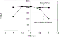
Fig. 8 is a cross-sectional view showing a state where the formation position of the p-type guard ring is shifted.
Fig. 9 is a diagram showing a change in withstand voltage according to the amount of shift in the formation position of the p-type guard ring.
Fig. 10A is a cross-sectional view showing a manufacturing process of the SiC semiconductor device shown in fig. 7.
Fig. 10B is a cross-sectional view showing a manufacturing process of the SiC semiconductor device subsequent to fig. 10A.
Fig. 10C is a cross-sectional view showing a manufacturing process of the SiC semiconductor device subsequent to fig. 10B.
Detailed Description
Embodiments of the present disclosure will be described below based on the drawings. In the following embodiments, the same or equivalent portions will be denoted by the same reference numerals.
(embodiment 1)
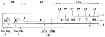
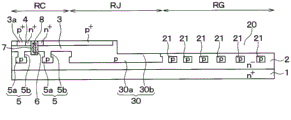
The SiC semiconductor device shown in fig. 1 has a cell region RC in which a MOSFET100 of a trench gate structure is formed and an outer peripheral region RO surrounding the cell region RC. The outer peripheral region RO has a guard ring portion RG, and a connection portion RJ disposed inside the guard ring portion RG, that is, between the cell region RC and the guard ring portion RG. In addition, fig. 1 is not a sectional view, but is partially shown hatched for easy viewing.
As shown in fig. 2, the SiC semiconductor device uses n composed of SiC + The mold substrate 1 is formed. At n + N composed of SiC is formed on the main surface of the substrate 1 by epitaxial growth or the like - A mold layer 2 and a p-type base region 3, and n is formed on the surface layer portion of the p-type base region 3 + Source region 4.
Regarding n + The n-type impurity concentration of the type substrate 1 is set to 1.0X10, for example 19 /cm 3 A substrate having a surface of (0001) Si and a direction of deviation (off) of < 11-20 > is used. Regarding n - Type layer 2, e.g., n-type impurity concentration is set to 5.0X10 15 ~2.0×10 16 /cm 3 . In the case of the present embodiment, the n - The type layer 2 constitutes an n-type layer serving as a drift layer.
The p-type body region 3 is formed such that the p-type impurity concentration is set to, for example, 2.0X10 at the portion where the channel region is formed 17 /cm 3 About, the thickness was 300nm. In the surface layer portion of the p-type base region 3, i.e., n + A p-type contact region 3a having a high concentration of p-type impurity is locally formed at a portion sandwiched between the source regions 4. n is n + The source region 4 is set to be a ratio n - The surface layer 2 has a high impurity concentration and is configured such that the n-type impurity concentration of the surface layer portion is, for example, 2.5X10 18 ~1.0×10 19 /cm 3 The thickness is about 0.5 μm.
In the cell region RC, in n + Leaving a p-type base region 3 and n on the surface side of the substrate 1 + A source region 4 extending through the p-type body region 3 and reaching the n-type body region RG - The mold layer 2 is formed with a recess 20. By adopting such a structure, the unit region RC and the connection portion RJ are formed as a mesa portion protruding more than the guard ring portion RG.
In addition, in the cell region RC, in n - Surface layer part of layer 2A p-type deep layer 5 corresponding to the 1 st deep layer having a higher p-type impurity concentration than the p-type base region 3 is formed. In more detail, the p-type deep layer 5 is formed from n - The position of the prescribed depth of the mold layer 2 is formed up to the surface, for example, by forming a pattern of n - The type layer 2 is formed by ion implantation of p-type impurities.
p-type deep layer 5 at n - The mold layers 2 are arranged at equal intervals in the form layer and are arranged so as to be separated from each other without intersecting points, thereby forming a stripe shape. The p-type base region 3 and n + A source region 4 is formed over the p-type deep layer 5.
Each of the p-type deep layers 5 is formed with the same impurity concentration, the same width and the same depth, and is configured such that, for example, the p-type impurity concentration is 1.0X10 17 ~1.0×10 19 /cm 3 The width is 0.7 μm and the depth is about 2.0 μm. Each p-type deep layer 5 is formed from one end to the other end of the cell region RC as shown in fig. 1. In the present embodiment, the p-type deep layer 5 extends in the same direction as the trench gate structure described later as a longitudinal direction, and is connected to a p-type deep layer 30 of a connecting portion RJ described later extending outside the cell region RC at both ends of the trench gate structure.
The extending direction of the p-type deep layer 5 is arbitrary, but in this embodiment, the direction is set to be the same as the offset direction < 11-20 >.
In addition, the p-type matrix region 3 and n + The source region 4 penetrates to n - The gate trench 6 having a width of 0.8 μm and a depth of 1.0 μm is formed in the pattern layer 2 so as to be shallower than the p-type deep layer 5. The p-type body regions 3 and n are arranged so as to be in contact with the side surfaces of the gate trench 6 + Source region 4. The gate trench 6 is formed in a linear layout having a width direction in the left-right direction of the paper surface in fig. 2, a length direction in the vertical direction of the paper surface, and a depth direction in the up-down direction of the paper surface. As shown in fig. 1, the gate trenches 6 are arranged so as to be sandwiched between the p-type deep layers 5, and are arranged in parallel at equal intervals to form a stripe shape.
In this case, the p-type body region 3 is laterally located in the gate trench 6As part of the operation of the vertical MOSFET100 + Source regions 4 and n - The channel region connected between the profile layers 2 functions. A gate insulating film 7 is formed on the inner wall surface of the gate trench 6 including the channel region. A gate electrode 8 made of doped polysilicon (Poly-Si) is formed on the surface of the gate insulating film 7, and the gate trench 6 is filled with the gate insulating film 7 and the gate electrode 8. Thereby, a trench gate structure is constituted. In fig. 1, the trench gate structure and the number of p-type deep layers 5 are reduced for easy viewing, but many similar structures are actually arranged.
In addition, in relation to n + The substrate 1 is arranged with n therebetween - Opposite side of the shaping layer 2, in particular at n + The source region 4, the p-type deep layer 5, and the gate electrode 8 have a source electrode 9 corresponding to the 1 st electrode, a gate wiring layer, and the like, which are not shown, formed on their surfaces with an interlayer insulating film 10 interposed therebetween. The source electrode 9 and the gate wiring layer are made of a plurality of metals such as Ni/Al. And, at least with n-type SiC, specifically n, of the plurality of metals + The portion of the source region 4 that is in contact with the n-type SiC ohmic contact is made of a metal. At least a portion of the plurality of metals in contact with the p-type SiC, specifically, the p-type contact region 3a is made of a metal capable of ohmic contact with the p-type SiC. The source electrode 9 and the gate wiring layer are electrically insulated by being separated from each other on the interlayer insulating film 10. The source electrode 9 and n are formed through a contact hole formed in the interlayer insulating film 10 + The source region 4 and the p-type contact region 3a are electrically contacted, and the gate wiring layer is electrically contacted with the gate electrode 8.
And at n + The back side of the substrate 1 is formed with a plurality of grooves n + The type substrate 1 is electrically connected to a drain electrode 11 corresponding to the 2 nd electrode. With this structure, the MOSFET100 having an n-channel inversion trench gate structure is formed. By disposing a plurality of cells in such a MOSFET100, the cell region RC is constituted.
On the other hand, the guard ring portion RG is penetrated through the p-type base region 3 to reach n as described above - The mold layer 2 is formed withRecess 20. Therefore, n is at a position separated from the cell region RC + The source region 4 and the p-type body region 3 are removed to form n - The mold layer 2 is exposed. Thus, it becomes n + A land portion protruding in an island shape from a part of the cell region RC and the connection portion RJ located inside the recess 20 in the thickness direction of the substrate 1.
In addition, n is located below the recess 20 - A plurality of p-type guard rings 21 are provided on the surface layer of the mold layer 2 so as to surround the cell region RC and the connection portion RJ. In the present embodiment, the p-type guard ring 21 is formed in a quadrangle having four corners rounded, but may be formed in another frame shape such as a circle. The p-type guard ring 21 is separated from n - The surface of the mold layer 2 is formed to a predetermined depth from the position thereof, e.g. by forming a pattern of n - The type layer 2 is formed by ion implantation of p-type impurities. In the case of the present embodiment, the lower surface of the p-type guard ring 21 is set to the same depth as the lower surface of the p-type deep layer 5, but is not formed up to n, unlike the p-type deep layer 5 - The upper surface of the mold layer 2 is deeper than the upper surface of the p-type deep layer 5.
In the present embodiment, the p-type guard ring 21 has the same structure as the p-type deep layer 5 except for the difference in depth. The p-type guard ring 21 is different from the p-type deep layer 5 formed in a straight line shape in that the upper surface shape is a line shape having a frame shape surrounding the cell region RC and the connection portion RJ, and the other points are the same. That is, the p-type guard ring 21 has the same impurity concentration and the same width as those of the p-type deep layer 5. The intervals between the p-type guard rings 21 may be equal intervals. Here, the distance between the p-type guard rings 21 is narrower on the cell region RC side and larger on the outer peripheral side, that is, on the cell region RC side, so that the equipotential lines are more toward the outer peripheral side to mitigate electric field concentration.
Although not shown, the guard ring portion RG having the outer Zhou Naiya structure surrounding the cell region RC is formed by providing an EQR structure on the outer periphery of the p-type guard ring 21 as needed.
Further, the cell region RC extends to the guard ring portion RGAs a connecting portion RJ, at the connecting portion RJ, at n - The surface layer portion of the mold layer 2 is formed with a p-type deep layer 30 corresponding to the 2 nd deep layer. The p-type deep layer 30 is fixed to the source potential by being in contact with the p-type body region 3. In the case of the present embodiment, as shown by solid hatching in fig. 1, the connection portion RJ is formed so as to surround the cell region RC, and a plurality of square p-type guard rings 21 each having a rounded four corners are formed so as to surround the outside of the connection portion RJ. The p-type deep layer 30 is formed in a solid hatched portion as the connection portion RJ, and is connected to the p-type deep layer 5 formed in the cell region RC.
Each p-type deep layer 30 is formed by, for example, forming a pair of n-type deep layers - The surface of the model layer 2 is ion-implanted with p-type impurities. The impurity concentration and depth of the p-type deep layer 30 are the same as those of the p-type deep layer 5.
Further, at the connecting portion RJ, also at n + An interlayer insulating film 10 is formed on the surface of the source region 4.
In this way, the structure having the connection portion RJ between the cell region RC and the guard ring portion RG is adopted, and the p-type deep layer 30 is formed in the connection portion RJ, thereby connecting the p-type deep layers 5 arranged on both sides of the trench gate structure. In this way, the equipotential lines can be prevented from excessively rising in the cell region RC, and the equipotential lines can extend from the cell region RC to the guard ring portion RG and can terminate at the guard ring portion RG.
With the above-described structure, the SiC semiconductor device of the present embodiment is configured. In the SiC semiconductor device having the above-described structure, when MOSFET100 is turned on, a channel region is formed in the surface portion of p-type body region 3 located on the side surface of gate trench 6 by controlling the voltage applied to gate electrode 8. Thus, via n + Source regions 4 and n - The mold layer 2 flows a current between the source electrode 9 and the drain electrode 11.
In addition, when the MOSFET100 is turned off, even if a high voltage is applied, the entry of an electric field to the bottom of the gate trench is suppressed by forming the p-type deep layer 5 and the p-type deep layer 30 up to a position deeper than the trench gate structure. Therefore, the electric field concentration at the bottom of the gate trench is relaxed. Thereby, breakdown of the gate insulating film 7 is prevented.
Further, the bulge of the equipotential lines is suppressed at the connection portion RJ, and is directed toward the guard ring portion RG side. In addition, in the guard ring portion RG, the p-type guard ring 21 gradually ends the equipotential lines in the outer circumferential direction, and the guard ring portion RG can also obtain a desired withstand voltage.
In the SiC semiconductor device according to the present embodiment, each p-type guard ring 21 is formed from n - The surface of the type layer 2 is separated from the position, and is thus protected by the p-type guard ring 21 and n - The boundary portion of the PN junction formed in the mold layer 2 is separated from the interlayer insulating film 10. Therefore, even if electric field concentration occurs in the PN junction, the interlayer insulating film 10 does not contact the PN junction, and therefore the intensity of the electric field applied to the interlayer insulating film 10 can be suppressed. Therefore, in the case of forming a protective film, not shown, on the interlayer insulating film 10 or above, an increase in the electric field strength at the outermost surface of the protective film can be suppressed, and the occurrence of the planar breakdown can be suppressed. In particular, since SiC is used as the semiconductor material, the electric field intensity at the outermost surface becomes higher by using a high voltage, but occurrence of the planar breakdown can be suppressed also in the case of using SiC.
For reference, in the case where the p-type guard ring 21 and the interlayer insulating film 10 were formed separately, and in the case where the p-type guard ring 21 and the interlayer insulating film 10 were formed in contact with each other, the change in the electric field intensity at the interface between the interlayer insulating film 10 and SiC was studied by simulation. Fig. 3 shows the results. Here, a case where 18 p-type guard rings 21 are formed was simulated.
As shown in the figure, when the p-type guard ring 21 is formed so as to be in contact with the interlayer insulating film 10, the p-type guard ring 21 has the same structure as the conventional one, and is formed on the outer peripheral side of each p-type guard ring 21 so as to be n - The electric field strength increases at the boundary position of the mold layer 2. Further, at the point where the electric field strength was maximum, 1.35MV/cm was shown to be a very large value.
On the other hand, in the case where the p-type guard ring 21 is formed separately from the interlayer insulating film 10 as in the present embodiment, the p-type guard ring 21 is formed on the outer peripheral side of each p-type guard ring 21 so as to be connected to n - Boundary position of the mold layer 2, electricThe field strength becomes large. However, the electric field strength was 0.98MV/cm at maximum, which is a sufficiently smaller value than the conventional structure. From this, it is understood that by adopting the structure of the present embodiment, the electric field intensity at the interface between the interlayer insulating film 10 and SiC can be suppressed.
Next, a method for manufacturing the SiC semiconductor device according to the present embodiment will be described with reference to fig. 4A to 4I.
[ procedure shown in FIG. 4A ]
First, as a semiconductor substrate, n is prepared + An n composed of SiC is epitaxially grown on the main surface of the substrate 1 - A semiconductor substrate of the mold layer 2. At this time, the method can be carried out by a method of forming a complex of + On the main surface of the substrate 1, n - The semiconductor substrate may be prepared by epitaxially growing the layer 2, or may be prepared by forming n in advance + On the main surface of the substrate 1, n is epitaxially grown - The so-called epitaxial substrate of the mold layer 2 serves as a semiconductor substrate.
(step shown in FIG. 4B)
Next, at n - A mask 40 is disposed on the mold layer 2, and the mask 40 is opened in the predetermined regions to be formed of the p-type deep layer 5, the p-type deep layer 30, and the p-type guard ring 21. Then, p-type impurities are ion-implanted using the mask 40. At this time, the range of ion implantation is adjusted so that p-type impurities are implanted to a ratio of n - The surface of the mold layer 2 is deep at a predetermined depth and is set at n - The surface of the model layer 2 is hardly implanted with p-type impurities. Thereby, the lower portion 5a of the p-type deep layer 5, the lower portion 30a of the p-type deep layer 30, and the p-type guard ring 21 are formed. Then, the mask 40 is removed.
(step shown in FIG. 4C)
Next, the mask 41 is disposed, and the mask 41 is opened in the region to be formed of the p-type deep layer 5 and the p-type deep layer 30. At this time, the mask 41 is not opened in the region where the p-type guard ring 21 is to be formed. Then, p-type impurities are ion-implanted using the mask 41. Thus, the upper portions 5b and 30b of the p-type deep layers 5 and 30 are formed and connected to the lower portions 5a and 30a of the p-type deep layers 5 and 30, respectively, to constitute the p-type deep layers 5 and 30. Then, the mask 41 is removed.
The widths of the upper portions 5b and 30b and the lower portions 5a and 30a of the p-type deep layers 5 and 30 may be the same, but may be different. In the present embodiment, the upper portions 5b and 30b of the p-type deep layer 5 and the p-type deep layer 30 are set to have a smaller width than the lower portions 5a and 30 a. The sequence of the steps shown in fig. 4B and the sequence of the steps shown in fig. 4C may be changed, and the steps shown in fig. 4C may be performed before the steps shown in fig. 4B.
[ procedure shown in FIG. 4D ]
Including the p-type deep layer 5, the p-type deep layer 30 and the p-type guard ring 21, at n - The p-type body region 3 is epitaxially grown over the mold layer 2.
(the step shown in FIG. 4E)
After a mask (not shown) is arranged on the p-type substrate region 3, n in the mask is set + The formation-scheduled-area opening of the source region 4 is formed. Then, n-type impurities are ion-implanted using the mask, thereby forming n + Source region 4. After the mask is removed, a mask, not shown, is rearranged, and the p-type contact region 3a in the mask is opened in the region to be formed. Then, p-type impurities are ion-implanted using the mask, thereby forming p-type contact regions 3a. Then, the mask is removed.
In addition, n is formed by ion implantation + The source region 4 and the p-type contact region 3a may be formed by epitaxial growth, or may be formed by ion implantation.
(step shown in FIG. 4F)
At n + After a mask (not shown) is formed over the source region 4, the p-type body region 3, and the like, the gate trench 6 and the recess 20 in the mask are opened. Then, anisotropic etching such as RIE (Reactive Ion Etching ) is performed using a mask, thereby simultaneously forming a specific n - A gate trench 6 and a recess 20 having a depth deeper in the upper surface of the mold layer 2 and shallower than the upper surface of the p-type guard ring 21.
The gate trench 6 and the recess 20 are formed at the same time, but they may be formed separately. In this case, since the gate trench 6 and the recess 20 can be set to different depths, they can be set to the most appropriate depths.
(step shown in FIG. 4G)
After removing the mask, for example, by performing thermal oxidation, a gate insulating film 7 is formed, and the inner wall surface of the gate trench 6 and n are formed by the gate insulating film 7 + The surface of the source region 4 is covered. Then, after depositing polysilicon doped with p-type impurities or n-type impurities, it is etched back, leaving polysilicon at least in the gate trench 6 to form the gate electrode 8. Thereby, a trench gate structure is constituted.
(step shown in FIG. 4H)
An interlayer insulating film 10 made of, for example, an oxide film is formed so as to cover the surfaces of the gate electrode 8 and the gate insulating film 7. After forming a mask, not shown, on the surface of the interlayer insulating film 10, a portion of the mask located between the gate electrodes 8, that is, a portion corresponding to the p-type contact region 3a, and the vicinity thereof are opened. Then, the interlayer insulating film 10 is patterned using a mask, thereby forming p-type contact regions 3a and n + The contact hole exposing the source region 4.
(step shown in FIG. 4I)
An electrode material composed of a laminated structure of a plurality of metals, for example, is formed on the surface of the interlayer insulating film 10. Then, the electrode material is patterned to form a source electrode 9, a gate wiring, and the like, which are not shown.
Although not shown in the drawings, the subsequent steps are performed by performing the steps represented by n + The step of forming the drain electrode 11 and the like on the back surface side of the mold substrate 1 completes the SiC semiconductor device of the present embodiment.
As described above, in the SiC semiconductor device of the present embodiment, each p-type guard ring 21 is formed from n - The surface of the pattern layer 2 is separated from the surface by p-type guard rings 21 and n - The boundary portion of the PN junction formed in the mold layer 2 is separated from the interlayer insulating film 10. Therefore, even if electric field concentration occurs at the PN junction portion, since the interlayer insulating film 10 is not in contact with the PN junction portion,therefore, the intensity of the electric field applied to the interlayer insulating film 10 can be suppressed. Therefore, in the case of forming a protective film, not shown, on the interlayer insulating film 10 or above, it is possible to suppress an increase in the electric field intensity at the outermost surface of the protective film, and to suppress the occurrence of the planar breakdown.
(embodiment 2)
The method for manufacturing the SiC semiconductor device of the present embodiment will be described with reference to the method for manufacturing the SiC semiconductor device of embodiment 1.
First, as in the step shown in fig. 4A described in embodiment 1, n is prepared as a semiconductor substrate + An n composed of SiC is epitaxially grown on the main surface of the substrate 1 - A semiconductor substrate of the mold layer 2. Then, the steps shown in fig. 5A to 5D are performed.
[ procedure shown in FIG. 5A ]
At n - A mask 50 is disposed on the pattern layer 2, and the mask 50 is opened in a predetermined region where the p-type deep layer 5 and the p-type deep layer 30 are formed. Then, p-type impurities are ion-implanted using the mask 50. Thereby, the p-type deep layer 5 and the p-type deep layer 30 are formed. Then, the mask 50 is removed.
[ procedure shown in FIG. 5B ]
Next, as a step shown in fig. 5B, n is - A mask 51 is disposed on the mold layer 2, and the mask 51 is opened in a region to be formed of the p-type deep layer 30 and the p-type guard ring 21. Then, p-type impurities are ion-implanted using the mask 51. At this time, the range of ion implantation is adjusted so that p-type impurities are implanted to a ratio of n - The surface of the mold layer 2 is deep at a predetermined depth and is formed such that at n - The surface of the model layer 2 is hardly implanted with p-type impurities. Thus, the p-type guard ring 21 can be formed, and a portion on the p-type guard ring 21 side in the p-type deep layer 30 can be formed. Thereafter, the mask 51 is removed.
Here, not only the p-type guard ring 21 but also a portion on the p-type guard ring 21 side in the p-type deep layer 30 is formed. This is because, when the p-type deep layer 30 is formed only by the process shown in fig. 5A, there is a possibility that the interval between the p-type deep layer 30 and the p-type guard ring 21 may vary depending on the mask alignment accuracy. In this way, by forming the p-type guard ring 21 at the same time as forming the p-type guard ring 21 at the end portion on the p-type guard ring 21 side in the p-type deep layer 30, the variation in the interval between the p-type deep layer 30 and the p-type guard ring 21 can be eliminated.
Thereafter, as the steps shown in fig. 5C and 5D, the steps shown in fig. 4D and 4E described in embodiment 1 are performed. Thereafter, although not shown, the steps subsequent to the step shown in fig. 4F described in embodiment 1 are also performed.
Thus, formation to n may also be performed separately - The formation steps of the p-type deep layer 5 and the p-type deep layer 30 up to the surface of the pattern layer 2, and the formation is performed only up to the time from n - And a step of forming a p-type guard ring 21 at a position away from the surface of the mold layer 2. Thus, the SiC semiconductor device having the structure shown in embodiment 1 can also be manufactured.
In addition, the end portion on the p-type guard ring 21 side in the p-type deep layer 30 is also formed at the same time when the p-type guard ring 21 is formed, whereby the variation in the interval between the p-type deep layer 30 and the p-type guard ring 21 can be eliminated. Of course, since the interval between the p-type deep layer 30 and the p-type guard ring 21 may be varied within an allowable range, in this case, only the p-type guard ring 21 may be formed in the process shown in fig. 5B.
(embodiment 3)
The method for manufacturing the SiC semiconductor device of the present embodiment will be described with reference to the method for manufacturing the SiC semiconductor device of embodiment 1.
First, as in the step shown in fig. 4A described in embodiment 1, n is prepared as a semiconductor substrate + Epitaxial growth on the main surface of the substrate 1N composed of SiC - A semiconductor substrate of the mold layer 2. In addition, the p-type deep layer 5 and the p-type deep layer 30 are formed by performing the same steps as those shown in fig. 5A described in embodiment 2. Then, the steps shown in fig. 6A to 6D are performed.
Specifically, as the step shown in fig. 6A, the p-type guard ring 21 is not formed, and the same step as that of fig. 4D is performed to form the p-type base region 3. Then, as the step shown in fig. 6B, n is formed by performing the same step as that shown in fig. 4E + A source region 4 and a p-type contact region 3a. Further, as the step shown in fig. 6C, the gate trench 6 and the recess 20 are formed by performing the same steps as those shown in fig. 4F.
Then, as a step shown in fig. 6D, at n - A mask 52 is disposed on the mold layer 2, and the mask 52 is opened in a region to be formed of the p-type deep layer 30 and the p-type guard ring 21. Then, p-type impurities are ion-implanted into the bottom surface of the recess 20 using the mask 52. At this time, the range of ion implantation is adjusted so that the p-type impurity is implanted into the recess 20 at a ratio n - The surface of the mold layer 2 is deep at a predetermined depth and is formed such that at n - The surface of the model layer 2 is hardly implanted with p-type impurities. Thus, the p-type guard ring 21 can be formed, and a portion on the p-type guard ring 21 side in the p-type deep layer 30 can be formed. Thereafter, the mask 52 is removed.
Here, the p-type guard ring 21 is formed, and the p-type guard ring 21 side end portion in the p-type deep layer 30 is also formed. As a result, as described in embodiment 2, the variation in the interval between the p-type deep layer 30 and the p-type guard ring 21 can be eliminated. However, in the manufacturing method of the present embodiment, the difference in the interval between the p-type deep layer 30 and the p-type guard ring 21 may be within an allowable range, and therefore, in this case, only the p-type guard ring 21 may be formed in the process shown in fig. 6D.
Although not shown in the drawings, the steps subsequent to the step shown in fig. 4G described in embodiment 1 are also performed.
In this way, the formation may be performed to n before the formation of the recess 20 - The surface of the layer 2 isThe formation steps of the p-type deep layer 5 and the p-type deep layer 30 are performed only from n after the formation of the recess 20 - And a step of forming a p-type guard ring 21 at a position away from the surface of the mold layer 2. Thus, the SiC semiconductor device having the structure shown in embodiment 1 can also be manufactured.
(embodiment 4)
As shown in fig. 7, the SiC semiconductor device of the present embodiment adopts the following structure: an n-type current spreading layer 60 is provided, n - The p-type body region 3 is formed above the mold layer 2 through the current spreading layer 60. That is, in the case of the present embodiment, the portions that are not used as the p-type deep layers 5 and 30 are used as the current spreading layer 60 at the positions corresponding to the upper portions 5b and 30b of the p-type deep layers 5 and 30. The current spreading layer 60 is also formed between the p-type guard ring 21 and the interlayer insulating film 10. For example, the n-type impurity concentration of the current dispersion layer 60 is 2.0X10 16 ~5.0×10 17 /cm 3 The thickness is 0.5-0.9 mu m. However, in the outer peripheral region RO, a part is removed when forming the recess 20 as described later, and thus the thickness is 0.2 to 0.6 μm.
The current spreading layer 60 is equal to n - The type layer 2 has a higher concentration of n-type impurities than the n-type impurities, i.e., a layer having a low resistance. If the n-type current spreading layer 60 is provided, a current can be distributed in a wider range in the current spreading layer 60, and the JFET resistance can be reduced.
Thus, n can also be used - The p-type body region 3 is formed above the mold layer 2 through the current spreading layer 60. In the case of adopting the structure having the current spreading layer 60 in this way, n - The type layer 2 and the current spreading layer 60 constitute an n-type layer which becomes a drift layer, n - The mold layer 2 constitutes layer 1 and the current spreading layer 60 constitutes layer 2.
Here, in the case of forming the current spreading layer 60Next, the current spreading layer 60 is ion-implanted to form the p-type deep layer 5 and the upper portions 5b and 30b of the p-type deep layer 30. At this time, it is considered that ion implantation is also performed to a portion of the current spreading layer 60 corresponding to the p-type guard ring 21. However, in this case, since the p-type guard ring 21 is in contact with the interlayer insulating film 10 as described above, there is a concern that a planar breakdown occurs. In addition, as shown in FIG. 8, the p-type guard ring 21 is formed on the n-type guard ring - The step of forming the lower portion 21a of the surface layer portion of the mold layer 2 and the step of forming the upper portion 21b of the current spreading layer 60 are different from each other. Therefore, the formation positions of the upper portion 21b and the lower portion 21a may be shifted due to mask shift at the time of the respective formation. As a result, the distance between adjacent p-type guard rings 21 becomes narrower, and if the offset is large, the electric field relaxing function of the p-type guard ring 21 cannot be exhibited, and the withstand voltage in the outer peripheral region RO cannot be obtained.
However, as in the present embodiment, if n is only - The p-type guard ring 21 is formed in the surface layer portion of the mold layer 2, and the p-type guard ring 21 is not formed in the current spreading layer 60, so that the mask deviation is not caused. Therefore, the interval between the adjacent p-type guard rings 21 can be set to a desired value, the electric field relaxing effect of the p-type guard rings 21 can be exhibited, and the withstand voltage in the outer peripheral region RO can be ensured.
Specifically, as shown in fig. 9, in the case of the structure in which the p-type guard ring 21 shown in fig. 8 is further formed in the current spreading layer 60, the withstand voltage varies depending on the amount of shift between the lower portion 21a and the upper portion 21b due to mask shift, and if the amount of shift increases, the withstand voltage is greatly reduced. In contrast, when the structure in which the p-type guard ring 21 is separated from the interlayer insulating film 10 without forming the p-type guard ring 21 in the current spreading layer 60 is employed as in the present embodiment, the breakdown voltage hardly decreases even if the mask misalignment occurs. In this way, by adopting the structure of the present embodiment, the withstand voltage in the outer peripheral region RO can be ensured.
Next, a method for manufacturing the SiC semiconductor device of the present embodiment will be described with reference to the method for manufacturing the SiC semiconductor device of embodiment 1.
First, the embodiment is described with reference to FIG. 4A described in embodiment 1In the same manner as in the step shown, n is prepared as a semiconductor substrate + An n composed of SiC is epitaxially grown on the main surface of the substrate 1 - A semiconductor substrate of the mold layer 2. Then, the process shown in fig. 10A to 10C is performed.
(step shown in FIG. 10A)
At n - A mask 71 is disposed above the pattern layer 2, and the mask 71 is opened in the region to be formed of the p-type deep layer 5, the p-type deep layer 30, and the p-type guard ring 21. Then, p-type impurities are ion-implanted using the mask 71. Thus, from n - The surface of the mold layer 2 is formed to a predetermined depth to form a lower portion 5a of the p-type deep layer 5 and a lower portion 30a of the p-type deep layer 30, and a p-type guard ring 21. Then, the mask 71 is removed.
[ procedure shown in FIG. 10B ]
Next, the upper region including the p-type deep layer 5, the p-type deep layer 30 and the p-type guard ring 21 is formed on the n-type - Epitaxial growth of the upper portion of the type layer 2, for example, to an n-type impurity concentration of 2.0X10 16 ~5.0×10 17 /cm 3 An n-type current spreading layer 60 having a thickness of 0.5 to 0.9 μm.
(step shown in FIG. 10C)
A mask 72 is disposed above the current spreading layer 60, and the mask 72 is opened in a region to be formed of the p-type deep layer 5 and the p-type deep layer 30. Then, p-type impurities are ion-implanted using the mask 72. Thereby, the p-type deep layer 5 and the p-type deep layer 30 are formed. Then, the mask 72 is removed.
Although not shown in the drawings, the steps shown in fig. 4C to 4E described in embodiment 1 are first performed in the subsequent steps. Thereby, p-type body regions 3, n are formed + A source region 4 and a p-type contact region 3a, and a gate trench 6 and a recess 20 are formed. At this time, when the gate trench 6 and the recess 20 are formed, the surface layer portion of the current spreading layer 60 is etched by about 0.3 μm so as to pass through the p-type base region 3 and reach the current spreading layer 60. Therefore, the thickness of the current spreading layer 60 is 0.2 to 0.6 μm in the recess 20 and in the lower portion of the gate trench 6. Wherein the etching amount is adjusted so that the current spreading layer 60 is not excessively removed to disappear.
Then, the SiC semiconductor device of this embodiment can also be manufactured by performing the steps subsequent to the step shown in fig. 4F described in embodiment 1.
(other embodiments)
The present disclosure has been described with reference to the above-described embodiments, but is not limited to the embodiments, and includes various modifications and modifications within the equivalent scope. In addition, various combinations and modes, and other combinations and modes including only one element, more than or less than the element, are also within the scope and spirit of the present disclosure.
For example, in the above embodiment, the MOSFET100 is exemplified as the semiconductor element provided in the cell region RC of the SiC semiconductor device. However, even if another semiconductor element is formed, the p-type guard ring 21 in the outer peripheral region RO may be formed so as not to contact the interlayer insulating film 10. Examples of such a semiconductor element include a schottky diode and an IGBT. In the above embodiments, the description has been made taking the MOSFET100 of the n-channel type in which the 1 st conductivity type is n-type and the 2 nd conductivity type is p-type as an example, but the MOSFET100 of the p-channel type in which the conductivity type of each constituent element is inverted may be used. The present invention is not limited to the trench gate structure element, and may be a planar element. In addition, the IGBT has n only with respect to the above embodiments + The conductivity type of the type substrate 1 is changed from n-type to p-type, and other structures and manufacturing methods are the same as those of the above embodiments.
In the above embodiments, the interval between the p-type guard rings 21 may be constant, or the width of each p-type guard ring 21 may be wider toward the outer periphery.
In the above embodiments, the method of forming the p-type deep layer 5, the p-type deep layer 30, and the p-type guard ring 21 is not limited to ion implantation, and other forming methods, such as epitaxial growth, may be used.
In embodiment 2, the value of n is as follows - The surface of the mold layer 2 is formed with a p-type deep layer 5 and a lower portion of the p-type deep layer 30 up to a predetermined depth5a, 30a and p-type guard ring 21, but may be formed only up to n - The surface of the mould layer 2 is located away from it. In this case, in the step shown in fig. 10C, n is oriented when the p-type deep layer 5 and the upper portions 5b and 30b of the p-type deep layer 30 are formed - The surface layer portion of the mold layer 2 is also implanted with p-type impurities. The upper portions 5b and 30b of the p-type deep layers 5 and 30 may be connected to the lower portions 5a and 30 a.
In the above embodiments, the case where SiC is used as the semiconductor material has been described, but the present disclosure can be applied to a semiconductor device using other semiconductor materials such as Si.
In addition, in the case of indicating the crystal orientation, a bar (-) should be attached to the desired number, but since there is a limitation in terms of the expression by the electronic application, in this specification, the bar is attached before the desired number.
Claims (8)
1. A semiconductor device having a cell Region (RC) in which a semiconductor element (100) is formed and an outer peripheral Region (RO) surrounding the outer periphery of the cell region, characterized in that,
The device comprises:
a substrate (1) having a front surface and a back surface, and comprising a semiconductor of the 1 st or 2 nd conductivity type;
a 1 st conductive layer (2, 60) formed on the surface of the substrate and made of a 1 st conductive semiconductor having an impurity concentration lower than that of the substrate;
a 1 st electrode (9) formed on the opposite side of the substrate from the 1 st conductive layer and provided on the semiconductor element; and
a 2 nd electrode (11) formed on the back surface side of the substrate and provided on the semiconductor element,
the outer peripheral region is provided with:
a linear guard ring (21) of the 2 nd conductivity type, formed in the surface layer portion of the 1 st conductivity type layer at a position separated from the surface of the 1 st conductivity type layer, and having a plurality of frame shapes surrounding the cell region; and
an interlayer insulating film (10) formed on the surface of the 1 st conductive layer,
the above-mentioned type 1 layer includes:
a 1 st layer (2) formed on the surface of the substrate and having the guard ring formed on a surface layer portion; and
and a layer 2 (60) formed on the guard ring and the layer 1 and having a higher concentration of the 1 st conductive type impurity than the layer 1.
2. The semiconductor device according to claim 1, wherein,
The semiconductor element described above is a MOSFET,
the MOSFET includes:
a substrate region of type 2, formed on the layer 2,
a 1 st conductive source region (4) formed on the base region, wherein the 1 st conductive impurity concentration is higher than that of the 1 st layer,
a trench gate structure including a gate insulating film (7) covering an inner wall surface of a gate trench (6) formed deeper than the body region from a surface of the source region, and a gate electrode (8) disposed on the gate insulating film;
the interlayer insulating film covers the gate electrode and the gate insulating film and has a contact hole;
a source electrode (9) electrically connected to the source region and the base region through the contact hole, the source electrode corresponding to the 1 st electrode; and
a drain electrode (11) formed on the back surface side of the substrate and corresponding to the 2 nd electrode,
the 2 nd layer forms a current dispersion layer.
3. A method for manufacturing a semiconductor device having a cell Region (RC) in which a semiconductor element (100) is formed and an outer peripheral Region (RO) surrounding the outer periphery of the cell region, characterized in that,
The method comprises the following steps:
forming a 1 st conductive layer (2, 60) on a substrate (1) comprising a 1 st conductive semiconductor or a 2 nd conductive semiconductor having a front surface and a rear surface, the 1 st conductive layer (2, 60) comprising a 1 st conductive semiconductor having a lower impurity concentration than the substrate;
forming a base region (3) made of a semiconductor of conductivity type 2 on the layer of conductivity type 1;
forming a source region (4) made of a semiconductor of a 1 st conductivity type on the base region, wherein the source region (4) has a 1 st conductivity type impurity concentration higher than that of the 1 st conductivity type layer;
forming a gate trench (6) extending from the surface of the source region through the body region to the 1 st conductive layer, forming a gate insulating film (7) in the gate trench, and forming a gate electrode (8) on the gate insulating film, thereby forming a trench gate structure;
forming a recess (20) penetrating the source region and the base region to the 1 st conductive layer in the outer peripheral region;
forming an interlayer insulating film (10) covering the trench gate structure, the source region, and the base region and covering the recess;
Forming a contact hole in the interlayer insulating film in the cell region, and then forming a source electrode (9) electrically connected to the source region and the base region through the contact hole; and
a drain electrode (11) is formed on the back surface side of the substrate,
the method for manufacturing the semiconductor device further includes the steps of:
ion implanting a 2 nd conductive impurity into the 1 st conductive layer in the cell region before forming the base region, thereby forming a 2 nd conductive deep layer (5) reaching the surface of the 1 st conductive layer; and
ion implanting a 2 nd conductive impurity into the 1 st conductive layer in the outer peripheral region before forming the base region, thereby forming a linear 2 nd conductive guard ring (21) at a position separated from the surface of the 1 st conductive layer by a depth, wherein the linear 2 nd conductive guard ring (21) is formed in a frame shape surrounding the cell region,
the step of forming the deep layer includes the steps of:
ion implanting a 2 nd conductive impurity into the 1 st conductive layer at a position separated from the surface of the 1 st conductive layer by a depth, thereby forming a deep lower portion (5 a) simultaneously with the formation of the guard ring; and
Ion implanting a 2 nd conductive impurity into the 1 st conductive layer to form an upper portion (5 b) which is connected to the lower portion and reaches the deep layer on the surface of the 1 st conductive layer.
4. A method for manufacturing a semiconductor device having a cell Region (RC) in which a semiconductor element (100) is formed and an outer peripheral Region (RO) surrounding the outer periphery of the cell region, characterized in that,
the method comprises the following steps:
forming a 1 st conductive layer (2, 60) on a substrate (1) comprising a 1 st conductive semiconductor or a 2 nd conductive semiconductor having a front surface and a rear surface, the 1 st conductive layer (2, 60) comprising a 1 st conductive semiconductor having a lower impurity concentration than the substrate;
forming a base region (3) made of a semiconductor of conductivity type 2 on the layer of conductivity type 1;
forming a source region (4) made of a semiconductor of a 1 st conductivity type on the base region, wherein the source region (4) has a 1 st conductivity type impurity concentration higher than that of the 1 st conductivity type layer;
forming a gate trench (6) extending from the surface of the source region through the body region to the 1 st conductive layer, forming a gate insulating film (7) in the gate trench, and forming a gate electrode (8) on the gate insulating film, thereby forming a trench gate structure;
Forming a recess (20) penetrating the source region and the base region to the 1 st conductive layer in the outer peripheral region;
forming an interlayer insulating film (10) covering the trench gate structure, the source region, and the base region and covering the recess;
forming a contact hole in the interlayer insulating film in the cell region, and then forming a source electrode (9) electrically connected to the source region and the base region through the contact hole; and
a drain electrode (11) is formed on the back surface side of the substrate,
the method for manufacturing the semiconductor device further includes the steps of:
ion implanting a 2 nd conductive impurity into the 1 st conductive layer in the cell region before forming the base region, thereby forming a 2 nd conductive deep layer (5) reaching the surface of the 1 st conductive layer; and
ion implanting a 2 nd conductive impurity into the 1 st conductive layer in the outer peripheral region before forming the base region, thereby forming a linear 2 nd conductive guard ring (21) at a position separated from the surface of the 1 st conductive layer by a depth, wherein the linear 2 nd conductive guard ring (21) is formed in a frame shape surrounding the cell region,
The step of forming the 1 st conductive type layer includes the steps of: the 1 st conductive layer is formed by forming a 1 st layer (2) formed on the surface of the substrate, and forming a 2 nd layer (60) having a 1 st conductive impurity concentration higher than that of the 1 st layer on the surface of the 1 st layer.
5. A method for manufacturing a semiconductor device having a cell Region (RC) in which a semiconductor element (100) is formed and an outer peripheral Region (RO) surrounding the outer periphery of the cell region, characterized in that,
the method comprises the following steps:
forming a 1 st conductive layer (2, 60) on a substrate (1) comprising a 1 st conductive semiconductor or a 2 nd conductive semiconductor having a front surface and a rear surface, the 1 st conductive layer (2, 60) comprising a 1 st conductive semiconductor having a lower impurity concentration than the substrate;
forming a base region (3) made of a semiconductor of conductivity type 2 on the layer of conductivity type 1;
forming a source region (4) made of a semiconductor of a 1 st conductivity type on the base region, wherein the source region (4) has a 1 st conductivity type impurity concentration higher than that of the 1 st conductivity type layer;
forming a gate trench (6) extending from the surface of the source region through the body region to the 1 st conductive layer, forming a gate insulating film (7) in the gate trench, and forming a gate electrode (8) on the gate insulating film, thereby forming a trench gate structure;
Forming a recess (20) penetrating the source region and the base region to the 1 st conductive layer in the outer peripheral region;
forming an interlayer insulating film (10) covering the trench gate structure, the source region, and the base region and covering the recess;
forming a contact hole in the interlayer insulating film in the cell region, and then forming a source electrode (9) electrically connected to the source region and the base region through the contact hole; and
a drain electrode (11) is formed on the back surface side of the substrate,
the method for manufacturing the semiconductor device further includes the steps of:
ion implanting a 2 nd conductive impurity into the 1 st conductive layer in the cell region before forming the base region, thereby forming a 2 nd conductive deep layer (5) reaching the surface of the 1 st conductive layer; and
ion implanting a 2 nd conductive impurity into the 1 st conductive layer in the outer peripheral region before forming the base region, thereby forming a linear 2 nd conductive guard ring (21) at a position separated from the surface of the 1 st conductive layer by a depth, wherein the linear 2 nd conductive guard ring (21) is formed in a frame shape surrounding the cell region,
The step of forming the 1 st conductive type layer includes the steps of: the 1 st conductive layer is formed by forming a 1 st layer (2) formed on the surface of the substrate, and forming a 2 nd layer (60) having a 1 st conductive impurity concentration higher than that of the 1 st layer on the surface of the 1 st layer,
further, the step of forming the deep layer includes the steps of:
ion implanting a 2 nd conductive type impurity into the 1 st layer before forming the 2 nd layer, thereby forming a lower portion (5 a) of the deep layer simultaneously with forming the guard ring; and
after the formation of the 2 nd layer, ion implanting a 2 nd conductive impurity into the 2 nd layer to form an upper portion (5 b) of the deep layer connected to the lower portion.
6. The method for manufacturing a semiconductor device according to claim 5, wherein,
the deep layer formed in the cell region is referred to as the 1 st deep layer,
the method comprises the following steps: ion implanting a 2 nd conductive impurity into a surface layer portion of the 1 st conductive layer in a connection portion (RJ) between the cell region and a guard ring portion (RG) forming the guard ring in the outer peripheral region to form a 2 nd deep layer (30) of the 2 nd conductive layer,
the step of forming the 2 nd deep layer comprises the following steps:
Forming the lower part of the 1 st deep layer simultaneously with forming the guard ring, and forming the lower part (30 a) of the 2 nd deep layer simultaneously; and
when forming the upper part of the 1 st deep layer, the upper part (30 b) of the 2 nd deep layer is also formed.
7. A method for manufacturing a semiconductor device having a cell Region (RC) in which a semiconductor element (100) is formed and an outer peripheral Region (RO) surrounding an outer periphery of the cell region, the method comprising the steps of:
forming a 1 st conductive layer (2, 60) on a substrate (1) comprising a 1 st conductive semiconductor or a 2 nd conductive semiconductor having a front surface and a rear surface, the 1 st conductive layer (2, 60) comprising a 1 st conductive semiconductor having a lower impurity concentration than the substrate;
forming a base region (3) made of a semiconductor of conductivity type 2 on the layer of conductivity type 1;
forming a source region (4) made of a semiconductor of a 1 st conductivity type on the base region, wherein the source region (4) has a 1 st conductivity type impurity concentration higher than that of the 1 st conductivity type layer;
forming a gate trench (6) extending from the surface of the source region through the body region to the 1 st conductive layer, forming a gate insulating film (7) in the gate trench, and forming a gate electrode (8) on the gate insulating film, thereby forming a trench gate structure;
Forming a recess (20) penetrating the source region and the base region to the 1 st conductive layer in the outer peripheral region;
forming an interlayer insulating film (10) covering the trench gate structure, the source region, and the base region and covering the recess;
forming a contact hole in the interlayer insulating film in the cell region, and then forming a source electrode (9) electrically connected to the source region and the base region through the contact hole; and
a drain electrode (11) is formed on the back surface side of the substrate,
the method for manufacturing the semiconductor device further includes the steps of:
ion implanting a 2 nd conductive impurity into the 1 st conductive layer in the cell region before forming the base region, thereby forming a 2 nd conductive deep layer (5) reaching the surface of the 1 st conductive layer; and
after forming the recess, ion implanting a 2 nd conductive impurity into the 1 st conductive layer at a position separated from the surface of the 1 st conductive layer by a depth to form a linear 2 nd conductive guard ring (21), wherein the linear 2 nd conductive guard ring (21) is formed in a frame shape surrounding the cell region,
The deep layer formed in the cell region is referred to as the 1 st deep layer,
the method comprises the following steps: ion implanting a 2 nd conductive impurity into a surface layer portion of the 1 st conductive layer in a connection portion (RJ) between the cell region and a guard ring portion (RG) forming the guard ring in the outer peripheral region to form a 2 nd deep layer (30) of the 2 nd conductive layer,
the step of forming the 2 nd deep layer comprises: at least a part of the 2 nd deep layer is also formed at the same time when the 1 st deep layer is formed.
8. The method for manufacturing a semiconductor device according to claim 7, wherein,
the step of forming the 2 nd deep layer comprises: when forming the guard ring, the guard ring side end portion in the 2 nd deep layer is also formed at the same time.
Applications Claiming Priority (3)
| Application Number | Priority Date | Filing Date | Title |
|---|---|---|---|
| JP2017-176776 | 2017-09-14 | ||
| JP2017176776A JP6870546B2 (en) | 2017-09-14 | 2017-09-14 | Semiconductor devices and their manufacturing methods |
| PCT/JP2018/034065 WO2019054459A1 (en) | 2017-09-14 | 2018-09-13 | Semiconductor device and manufacturing process therefor |
Publications (2)
| Publication Number | Publication Date |
|---|---|
| CN111344866A CN111344866A (en) | 2020-06-26 |
| CN111344866B true CN111344866B (en) | 2023-06-16 |
Family
ID=65722758
Family Applications (1)
| Application Number | Title | Priority Date | Filing Date |
|---|---|---|---|
| CN201880058819.XA Active CN111344866B (en) | 2017-09-14 | 2018-09-13 | Semiconductor device and method for manufacturing the same |
Country Status (4)
| Country | Link |
|---|---|
| US (1) | US10964809B2 (en) |
| JP (1) | JP6870546B2 (en) |
| CN (1) | CN111344866B (en) |
| WO (1) | WO2019054459A1 (en) |
Families Citing this family (8)
| Publication number | Priority date | Publication date | Assignee | Title |
|---|---|---|---|---|
| CN112349771A (en) * | 2020-09-30 | 2021-02-09 | 湖南大学 | Buried layer type terminal structure of silicon carbide device and preparation method thereof |
| JP2023548541A (en) * | 2020-11-06 | 2023-11-17 | アリゴス セラピューティクス,インコーポレーテッド | Oxindole and its usage |
| JP2022168904A (en) * | 2021-04-27 | 2022-11-09 | 富士電機株式会社 | Silicon carbide semiconductor device and method for manufacturing silicon carbide semiconductor device |
| CN114335141A (en) * | 2021-12-20 | 2022-04-12 | 深圳基本半导体有限公司 | Composite field limiting ring terminal structure and preparation method |
| CN115472495A (en) * | 2022-07-21 | 2022-12-13 | 上海林众电子科技有限公司 | Preparation method of power chip termination area and preparation method of power chip |
| CN115498013B (en) * | 2022-07-21 | 2024-04-26 | 上海林众电子科技有限公司 | Preparation method of power chip termination region, structure of termination region and power chip |
| CN115020240B (en) * | 2022-08-03 | 2023-03-28 | 上海维安半导体有限公司 | Preparation method and structure of low-voltage super-junction trench MOS device |
| JP2024060452A (en) * | 2022-10-19 | 2024-05-02 | 株式会社デンソー | Semiconductor device and its manufacturing method |
Citations (9)
| Publication number | Priority date | Publication date | Assignee | Title |
|---|---|---|---|---|
| JP2000022176A (en) * | 1998-06-30 | 2000-01-21 | Toshiba Corp | Semiconductor device for power |
| JP2001144292A (en) * | 1999-11-17 | 2001-05-25 | Denso Corp | Silicon carbide semiconductor device |
| JP2008004643A (en) * | 2006-06-20 | 2008-01-10 | Toshiba Corp | Semiconductor device |
| CN101872790A (en) * | 2009-04-27 | 2010-10-27 | 得诣科技股份有限公司 | Schottky diode element having epitaxial guard ring and manufacturing method thereof |
| JP2014170778A (en) * | 2013-03-01 | 2014-09-18 | Sumitomo Electric Ind Ltd | Silicon carbide semiconductor device |
| CN104380471A (en) * | 2012-06-13 | 2015-02-25 | 株式会社电装 | Silicon carbide semiconductor device and method for producing same |
| JP2015076592A (en) * | 2013-10-11 | 2015-04-20 | 住友電気工業株式会社 | Silicon carbide semiconductor device and manufacturing method of the same |
| EP3012870A1 (en) * | 2014-10-20 | 2016-04-27 | ABB Technology AG | Edge termination for high voltage semiconductor devices |
| WO2016194280A1 (en) * | 2015-05-29 | 2016-12-08 | 株式会社デンソー | Semiconductor device and method for manufacturing same |
Family Cites Families (5)
| Publication number | Priority date | Publication date | Assignee | Title |
|---|---|---|---|---|
| US7737469B2 (en) | 2006-05-16 | 2010-06-15 | Kabushiki Kaisha Toshiba | Semiconductor device having superjunction structure formed of p-type and n-type pillar regions |
| JP5224289B2 (en) * | 2009-05-12 | 2013-07-03 | 三菱電機株式会社 | Semiconductor device |
| JP6231396B2 (en) | 2014-02-10 | 2017-11-15 | トヨタ自動車株式会社 | Semiconductor device and manufacturing method of semiconductor device |
| JP6428489B2 (en) | 2014-09-16 | 2018-11-28 | 株式会社デンソー | Silicon carbide semiconductor device and manufacturing method thereof |
| JP6740759B2 (en) * | 2016-07-05 | 2020-08-19 | 株式会社デンソー | Silicon carbide semiconductor device and manufacturing method thereof |
-
2017
- 2017-09-14 JP JP2017176776A patent/JP6870546B2/en active Active
-
2018
- 2018-09-13 WO PCT/JP2018/034065 patent/WO2019054459A1/en active Application Filing
- 2018-09-13 CN CN201880058819.XA patent/CN111344866B/en active Active
-
2020
- 2020-03-12 US US16/816,463 patent/US10964809B2/en active Active
Patent Citations (9)
| Publication number | Priority date | Publication date | Assignee | Title |
|---|---|---|---|---|
| JP2000022176A (en) * | 1998-06-30 | 2000-01-21 | Toshiba Corp | Semiconductor device for power |
| JP2001144292A (en) * | 1999-11-17 | 2001-05-25 | Denso Corp | Silicon carbide semiconductor device |
| JP2008004643A (en) * | 2006-06-20 | 2008-01-10 | Toshiba Corp | Semiconductor device |
| CN101872790A (en) * | 2009-04-27 | 2010-10-27 | 得诣科技股份有限公司 | Schottky diode element having epitaxial guard ring and manufacturing method thereof |
| CN104380471A (en) * | 2012-06-13 | 2015-02-25 | 株式会社电装 | Silicon carbide semiconductor device and method for producing same |
| JP2014170778A (en) * | 2013-03-01 | 2014-09-18 | Sumitomo Electric Ind Ltd | Silicon carbide semiconductor device |
| JP2015076592A (en) * | 2013-10-11 | 2015-04-20 | 住友電気工業株式会社 | Silicon carbide semiconductor device and manufacturing method of the same |
| EP3012870A1 (en) * | 2014-10-20 | 2016-04-27 | ABB Technology AG | Edge termination for high voltage semiconductor devices |
| WO2016194280A1 (en) * | 2015-05-29 | 2016-12-08 | 株式会社デンソー | Semiconductor device and method for manufacturing same |
Also Published As
| Publication number | Publication date |
|---|---|
| CN111344866A (en) | 2020-06-26 |
| WO2019054459A1 (en) | 2019-03-21 |
| JP2019054087A (en) | 2019-04-04 |
| JP6870546B2 (en) | 2021-05-12 |
| US10964809B2 (en) | 2021-03-30 |
| US20200227549A1 (en) | 2020-07-16 |
Similar Documents
| Publication | Publication Date | Title |
|---|---|---|
| CN111344866B (en) | Semiconductor device and method for manufacturing the same | |
| JP5812029B2 (en) | Silicon carbide semiconductor device and manufacturing method thereof | |
| CN109417088B (en) | Silicon carbide semiconductor device and method for manufacturing same | |
| CN109417087B (en) | Silicon carbide semiconductor device and method for manufacturing same | |
| CN110914998B (en) | Semiconductor device and method for manufacturing the same | |
| JP6673174B2 (en) | Silicon carbide semiconductor device and method of manufacturing the same | |
| US10784335B2 (en) | Silicon carbide semiconductor device and manufacturing method therefor | |
| JP2013038308A (en) | Silicon carbide semiconductor device and manufacturing method therefor | |
| CN109417089B (en) | Silicon carbide semiconductor device and method for manufacturing same | |
| WO2019044921A1 (en) | Silicon carbide semiconductor device and method for manufacturing same | |
| US10714611B2 (en) | Silicon carbide semiconductor device | |
| CN111133588B (en) | Semiconductor device and method for manufacturing the same | |
| CN113826213B (en) | Silicon carbide semiconductor device and method for manufacturing same | |
| WO2019009091A1 (en) | Semiconductor device and method for manufacturing same | |
| JP2023035249A (en) | Semiconductor device and manufacturing method of the same |
Legal Events
| Date | Code | Title | Description |
|---|---|---|---|
| PB01 | Publication | ||
| PB01 | Publication | ||
| SE01 | Entry into force of request for substantive examination | ||
| SE01 | Entry into force of request for substantive examination | ||
| GR01 | Patent grant | ||
| GR01 | Patent grant |