CN111146292B - A vertical GaN MOS with integrated freewheeling diode - Google Patents

A vertical GaN MOS with integrated freewheeling diode Download PDF

Info

Publication number
CN111146292B
CN111146292B CN202010051717.4A CN202010051717A CN111146292B CN 111146292 B CN111146292 B CN 111146292B CN 202010051717 A CN202010051717 A CN 202010051717A CN 111146292 B CN111146292 B CN 111146292B
Authority
CN
China
Prior art keywords
type
insulating medium
region
diode
integrated
Prior art date
Legal status (The legal status is an assumption and is not a legal conclusion. Google has not performed a legal analysis and makes no representation as to the accuracy of the status listed.)
Active
Application number
CN202010051717.4A
Other languages
Chinese (zh)
Other versions
CN111146292A (en
Inventor
罗小蓉
孙涛
欧阳东法
郗路凡
杨超
邓思宇
魏杰
张波
Current Assignee (The listed assignees may be inaccurate. Google has not performed a legal analysis and makes no representation or warranty as to the accuracy of the list.)
University of Electronic Science and Technology of China
Original Assignee
University of Electronic Science and Technology of China
Priority date (The priority date is an assumption and is not a legal conclusion. Google has not performed a legal analysis and makes no representation as to the accuracy of the date listed.)
Filing date
Publication date
Application filed by University of Electronic Science and Technology of China filed Critical University of Electronic Science and Technology of China
Priority to CN202010051717.4A priority Critical patent/CN111146292B/en
Publication of CN111146292A publication Critical patent/CN111146292A/en
Application granted granted Critical
Publication of CN111146292B publication Critical patent/CN111146292B/en
Active legal-status Critical Current
Anticipated expiration legal-status Critical

Links

Images

Classifications

    • HELECTRICITY
    • H10SEMICONDUCTOR DEVICES; ELECTRIC SOLID-STATE DEVICES NOT OTHERWISE PROVIDED FOR
    • H10DINORGANIC ELECTRIC SEMICONDUCTOR DEVICES
    • H10D84/00Integrated devices formed in or on semiconductor substrates that comprise only semiconducting layers, e.g. on Si wafers or on GaAs-on-Si wafers
    • H10D84/101Integrated devices comprising main components and built-in components, e.g. IGBT having built-in freewheel diode
    • H10D84/141VDMOS having built-in components
    • H10D84/143VDMOS having built-in components the built-in components being PN junction diodes
    • H10D84/144VDMOS having built-in components the built-in components being PN junction diodes in antiparallel diode configurations

Landscapes

  • Metal-Oxide And Bipolar Metal-Oxide Semiconductor Integrated Circuits (AREA)

Abstract

本发明属于功率半导体技术领域,涉及一种具有集成续流二极管的纵向GaN MOS。集成的二极管在源极电压为0时,利用源电极金属与GaN半导体之间功函数差耗尽集成的二极管阳极和阴极之间的导电沟道,实现二极管的关断。在反向续流时,源电极所加电压大于电压临界值后,耗尽区变窄,集成的二极管导通;当源极电压进一步增大,凸出部分的漂移区侧壁开始出现高浓度电子积累层。相比与纵向GaN MOS寄生的体二极管,集成的二极管具有低的开启电压、低的导通压降及快的反向恢复特性。在正向导通或者正向阻断时,集成的二极管处于关断状态,不影响纵向GaN MOS的导通及耐压特性。相比传统平面栅纵向GaN MOS,本发明没有占用额外的芯片面积。

Figure 202010051717

The invention belongs to the technical field of power semiconductors, and relates to a vertical GaN MOS with an integrated freewheeling diode. When the source voltage of the integrated diode is 0, the conduction channel between the anode and the cathode of the integrated diode is depleted by using the work function difference between the source electrode metal and the GaN semiconductor, and the diode is turned off. During reverse freewheeling, after the voltage applied to the source electrode is greater than the critical value of the voltage, the depletion region becomes narrower and the integrated diode is turned on; when the source voltage further increases, the sidewall of the drift region of the protruding part begins to appear high concentration electron accumulation layer. Compared with the parasitic body diode of vertical GaN MOS, the integrated diode has low turn-on voltage, low turn-on voltage drop and fast reverse recovery characteristics. During forward conduction or forward blocking, the integrated diode is in an off state, which does not affect the conduction and withstand voltage characteristics of the vertical GaN MOS. Compared with the conventional planar gate vertical GaN MOS, the present invention does not occupy additional chip area.

Figure 202010051717

Description

Longitudinal GaN MOS with integrated freewheeling diode
Technical Field
The invention belongs to the technical field of power semiconductors, and relates to a longitudinal GaN MOS with an integrated freewheeling diode.
Background
Power field effect transistors (MOSFETs) have better switching performance than bipolar devices and are therefore widely used in the field of high frequency power switching. The parasitic PN junction body diode of the power field effect transistor can conduct current in the reverse direction and can be used as reverse follow current of the power converter. However, the GaN forbidden band width is larger than 3.4eV, so the turn-on voltage of the PN junction body diode is larger, and meanwhile, minority carriers affect the reverse recovery characteristic, resulting in larger power loss. One solution is to reduce the carrier lifetime in the drift region to improve the reverse recovery characteristics, but at the same time increase the forward conduction voltage drop and leakage current. Another solution is to integrate the schottky diode, but the schottky contact takes up additional chip area, increasing leakage current, while temperature has a greater impact on schottky performance.
Disclosure of Invention
In view of the above problems, the present invention proposes a vertical GaN MOS with an integrated freewheeling diode.
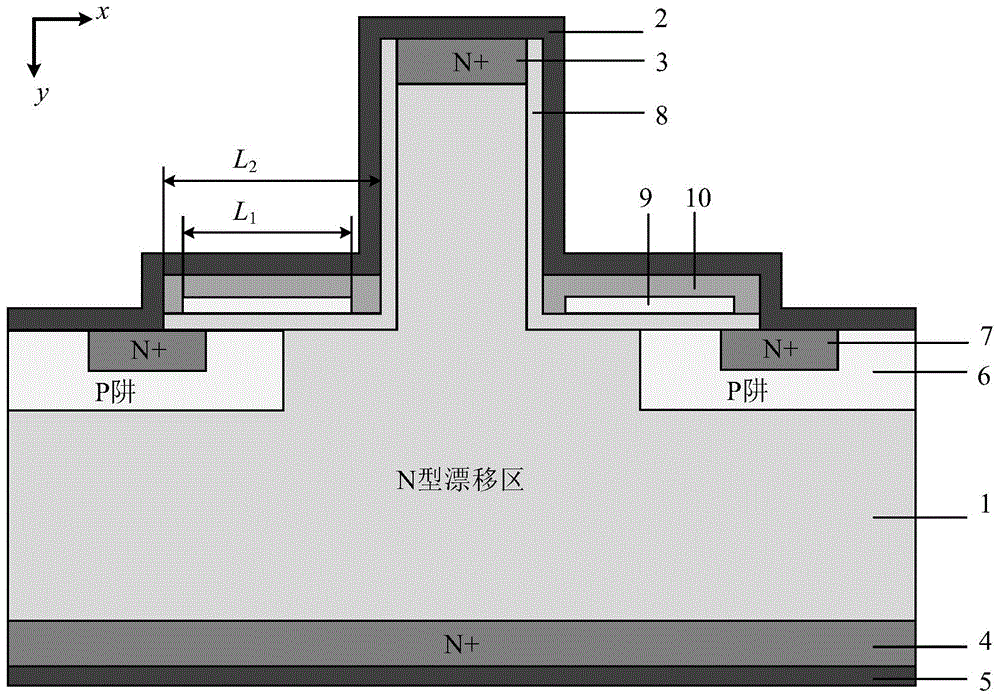
The technical solution of the present invention is, as shown in fig. 1, a vertical GaN MOS with an integrated freewheeling diode, comprising, from top to bottom: the transistor comprises a source electrode 2, a first N-type high-doping region 3, an N-type drift region 1, an N-type drain region 4 and a drain electrode 5, wherein the middle part of the N-type drift region 1 protrudes upwards to form an inverted T-shaped structure, and the top of the protrusion of the N-type drift region 1 is provided with the first N-type high-doping region 3;
the upper surface of the N-type drift region 1 except the convex part is provided with a P-type well region 6, and the upper part of the P-type well region 6 is provided with a second N-type highly doped region 7; a first insulating medium 8 covers the side walls of the convex parts of the P-type well region 6, the second N-type high-doping region 7 and the N-type drift region 1, and the first insulating medium 8 is in an L-shaped structure; the first insulating medium 8 covers one side of the second N-type highly-doped region 7 close to the convex part of the N-type drift region 1, but does not completely cover the second N-type highly-doped region 7; the lateral part of the first insulating medium 8 is covered with a gate electrode 9, the length L of the gate electrode 91Is smaller than the length L of the lateral portion of the first insulating medium 82(ii) a Covering the gate electrode 9 with a second insulating medium 10, wherein the second insulating medium 10 is partially in contact with the first insulating medium 8; the source electrode 2 covers the first N-type highly doped region 3, the first insulating medium 8, the second insulating medium 10, the second N-type highly doped region 7 and the P-type well region 6;
the source electrode 2, the first N-type highly doped region 3, the first insulating medium 8, the N-type drift region 1, the N-type drain region 4 and the drain electrode 5 form a freewheeling diode. In the scheme of the invention, the freewheeling diode is integrated, so that the integrated diode is conducted when freewheeling is carried out reversely, and the integrated diode has the characteristics of low starting voltage, low conduction voltage drop and quick reverse recovery. When the GaN MOS is conducted in the forward direction, the integrated diode is in an off state, and the forward conduction of the GaN MOS is not influenced. Compared with the traditional planar gate field effect transistor, the invention does not occupy additional chip area.
Compared with a body diode with a traditional GaN MOS structure, the integrated diode has the advantages of lower starting voltage, smaller conduction loss and faster reverse recovery; compared with the GaN MOS structure integrated Schottky diode, the invention does not occupy extra chip area, and simultaneously avoids the premature breakdown of the GaN Schottky diode caused by the electric leakage of the Schottky junction. In addition, the barrier height of the channel region is almost constant with temperature, and the integrated diode has high temperature stability.
Drawings
Fig. 1 is a schematic structural view of the present invention.
Detailed Description
The construction of the present invention has been described in detail in the summary of the invention, and the technical advances achieved by the present invention will be described in detail below in conjunction with the differences in the operational principles of the present invention from the conventional art.
The working principle of the invention is as follows: when the current flows reversely, the source electrode 2 is at a positive voltage relative to the drain electrode 5, so that the depletion region between the source electrode 2 and the N-type drift region 1 is reduced, and an electron inversion layer is further formed on the surface of the N-type doped region 1 on the side wall of the first insulating medium 8, so that a current path is formed between the source electrode 2 and the drain electrode 5, and the integrated diode is conducted. Compared with a parasitic PN junction body diode of a GaN MOS structure, the GaN MOS structure has smaller starting voltage and faster reverse recovery characteristic; compared with an integrated Schottky diode, the Schottky diode has lower leakage current and higher breakdown voltage. In addition, the invention does not occupy additional chip area.

Claims (1)

1.一种具有集成续流二极管的纵向GaN MOS,从上到下包括:源电极(2)、第一N型高掺杂区(3)、N型漂移区(1)、N型漏区(4)及漏电极(5),所述N型漂移区(1)中部向上凸起从而呈倒“T”字形结构,在N型漂移区(1)凸起的顶部与源电极(2)之间有第一N型高掺杂区(3);1. A vertical GaN MOS with an integrated freewheeling diode, comprising from top to bottom: a source electrode (2), a first N-type highly doped region (3), an N-type drift region (1), an N-type drain region (4) and the drain electrode (5), the middle part of the N-type drift region (1) is raised upward to form an inverted "T"-shaped structure, and the top of the protrusion of the N-type drift region (1) is connected to the source electrode (2) There is a first N-type highly doped region (3) therebetween; 所述N型漂移区(1)上层两端设置有P型阱区(6),P型阱区(6)与N型漂移区(1)凸起部分之间有间距,所述P型阱区(6)上层中部设置有第二N型高掺杂区(7);在第一N型高掺杂区(3)和N型漂移区(1)凸起部分的侧壁上覆盖有第一绝缘介质(8),且第一绝缘介质(8)沿N型漂移区(1)上表面向远离N型漂移区(1)凸起部分的方向延伸并覆盖部分P型阱区(6)、第二N型高掺杂区(7)的上表面,第一绝缘介质(8)呈“L”字型结构;所述第一绝缘介质(8)的横向部分上表面具有栅电极(9),所述栅电极(9)的长度L1小于第一绝缘介质(8)的横向部分的长度L2;在栅电极(9)上覆盖有第二绝缘介质(10),所述第二绝缘介质(10)沿栅电极(9)的两侧向下延伸至与第一绝缘介质(8)上表面接触,第二绝缘介质(10)还与第一绝缘介质(8)的垂直部分接触;所述源电极(2)覆盖在第一N型高掺杂区(3)、第一绝缘介质(8)、第二绝缘介质(10)、第二N型高掺杂区(7)及P型阱区(6)上表面;Both ends of the upper layer of the N-type drift region (1) are provided with P-type well regions (6), and there is a distance between the P-type well region (6) and the raised portion of the N-type drift region (1), and the P-type well regions (6) A second N-type highly doped region (7) is arranged in the middle of the upper layer of the region (6); An insulating medium (8), and the first insulating medium (8) extends along the upper surface of the N-type drift region (1) in a direction away from the convex portion of the N-type drift region (1) and covers part of the P-type well region (6) 2. On the upper surface of the second N-type highly doped region (7), the first insulating medium (8) has an "L"-shaped structure; the upper surface of the lateral part of the first insulating medium (8) has a gate electrode (9). ), the length L 1 of the gate electrode (9) is smaller than the length L 2 of the lateral part of the first insulating medium (8); the gate electrode (9) is covered with a second insulating medium (10), the second insulating medium (10) is The insulating medium (10) extends down along both sides of the gate electrode (9) to contact the upper surface of the first insulating medium (8), and the second insulating medium (10) is also in contact with the vertical part of the first insulating medium (8) ; the source electrode (2) covers the first N-type highly doped region (3), the first insulating medium (8), the second insulating medium (10), the second N-type highly doped region (7) and The upper surface of the P-type well region (6); 其中,源电极(2)、第一N型高掺杂区(3)、第一绝缘介质(8)、N型漂移区(1)、N型漏区(4)与漏电极(5)构成续流二极管。Wherein, a source electrode (2), a first N-type highly doped region (3), a first insulating medium (8), an N-type drift region (1), an N-type drain region (4) and a drain electrode (5) are formed Freewheeling diode.
CN202010051717.4A 2020-01-17 2020-01-17 A vertical GaN MOS with integrated freewheeling diode Active CN111146292B (en)

Priority Applications (1)

Application Number Priority Date Filing Date Title
CN202010051717.4A CN111146292B (en) 2020-01-17 2020-01-17 A vertical GaN MOS with integrated freewheeling diode

Applications Claiming Priority (1)

Application Number Priority Date Filing Date Title
CN202010051717.4A CN111146292B (en) 2020-01-17 2020-01-17 A vertical GaN MOS with integrated freewheeling diode

Publications (2)

Publication Number Publication Date
CN111146292A CN111146292A (en) 2020-05-12
CN111146292B true CN111146292B (en) 2021-05-14

Family

ID=70525680

Family Applications (1)

Application Number Title Priority Date Filing Date
CN202010051717.4A Active CN111146292B (en) 2020-01-17 2020-01-17 A vertical GaN MOS with integrated freewheeling diode

Country Status (1)

Country Link
CN (1) CN111146292B (en)

Families Citing this family (3)

* Cited by examiner, † Cited by third party
Publication number Priority date Publication date Assignee Title
CN113035863B (en) * 2021-03-03 2022-06-03 浙江大学 Power integrated chip with longitudinal channel structure
WO2025121737A1 (en) * 2023-12-06 2025-06-12 주식회사 엘엑스세미콘 Power semiconductor device and power conversion device including same
CN119364844B (en) * 2024-10-11 2025-10-24 电子科技大学 An enhancement-mode GaN vertical field-effect transistor with reverse freewheeling capability

Family Cites Families (6)

* Cited by examiner, † Cited by third party
Publication number Priority date Publication date Assignee Title
DE102004036278B4 (en) * 2004-07-27 2006-07-06 Siemens Ag Semiconductor device and method for operating the semiconductor device as an electronic switch
CN102664197B (en) * 2012-06-05 2014-08-06 长安大学 JFET (Junction Field Effect Transistor) and manufacturing method thereof, and micro inverter using JFET
US9064887B2 (en) * 2012-09-04 2015-06-23 Infineon Technologies Austria Ag Field-effect semiconductor device and manufacturing method therefor
JP6593294B2 (en) * 2016-09-28 2019-10-23 トヨタ自動車株式会社 Semiconductor device
CN108198857A (en) * 2017-12-28 2018-06-22 北京世纪金光半导体有限公司 A kind of silicon carbide MOSFET device structure cell of integrated convex block shape Schottky diode
CN109742135B (en) * 2018-12-03 2022-05-20 北京大学深圳研究生院 Silicon carbide MOSFET device and preparation method thereof

Also Published As

Publication number Publication date
CN111146292A (en) 2020-05-12

Similar Documents

Publication Publication Date Title
CN113130627B (en) Silicon carbide fin-shaped gate MOSFET integrated with channel diode
US7719053B2 (en) Semiconductor device having increased gate-source capacity provided by protruding electrode disposed between gate electrodes formed in a trench
US8441046B2 (en) Topside structures for an insulated gate bipolar transistor (IGBT) device to achieve improved device performances
KR101921844B1 (en) Semiconductor device
US8816355B2 (en) Semiconductor device
CN109830524B (en) A Very Low Reverse Recovery Charge Superjunction Power VDMOS
US10686062B2 (en) Topside structures for an insulated gate bipolar transistor (IGBT) device to achieve improved device performances
CN111668212B (en) Semiconductor device with a semiconductor device having a plurality of semiconductor chips
CN111146292B (en) A vertical GaN MOS with integrated freewheeling diode
US20210202724A1 (en) Fortified trench planar mos power transistor
US20150084121A1 (en) Transistor Device with a Field Electrode
CN113990923B (en) Silicon carbide double-groove MOSFET (Metal-oxide-semiconductor field Effect transistor) integrated with trench diode
JP7512920B2 (en) Semiconductor device and its manufacturing method
CN111211160B (en) Vertical GaN power diode
WO2019085850A1 (en) Igbt power device
CN111933711B (en) SBD integrated super-junction MOSFET
CN113471290A (en) Tunneling-assisted conduction silicon/silicon carbide heterojunction MOSFET (Metal-oxide-semiconductor field Effect transistor) power device
CN111223937B (en) A GaN Vertical Field Effect Transistor with Integrated Freewheeling Diode
US11296213B2 (en) Reverse-conducting igbt having a reduced forward recovery voltage
CN114447101B (en) Vertical GaN MOSFET integrated with freewheeling channel diode
CN113053992B (en) Cell structure of silicon carbide MOSFET device and power semiconductor device
KR102392277B1 (en) Power Semiconductor Device
CN117153884A (en) A GaN vertical field effect transistor with reverse conduction capability
CN116646388A (en) Shielded gate MOSFET structure
CN115602706A (en) VDMOSFET Device with Source and Mesa Structure Integrated Schottky Diode

Legal Events

Date Code Title Description
PB01 Publication
PB01 Publication
SE01 Entry into force of request for substantive examination
GR01 Patent grant
GR01 Patent grant