CN110640552B - Processing method of easily-cleaved semiconductor crystal - Google Patents
Processing method of easily-cleaved semiconductor crystal Download PDFInfo
- Publication number
- CN110640552B CN110640552B CN201910867396.2A CN201910867396A CN110640552B CN 110640552 B CN110640552 B CN 110640552B CN 201910867396 A CN201910867396 A CN 201910867396A CN 110640552 B CN110640552 B CN 110640552B
- Authority
- CN
- China
- Prior art keywords
- grinding
- feed
- force
- gallium oxide
- fine
- Prior art date
- Legal status (The legal status is an assumption and is not a legal conclusion. Google has not performed a legal analysis and makes no representation as to the accuracy of the status listed.)
- Active
Links
- 239000013078 crystal Substances 0.000 title claims abstract description 26
- 239000004065 semiconductor Substances 0.000 title claims abstract description 17
- 238000003672 processing method Methods 0.000 title claims description 11
- AJNVQOSZGJRYEI-UHFFFAOYSA-N digallium;oxygen(2-) Chemical compound [O-2].[O-2].[O-2].[Ga+3].[Ga+3] AJNVQOSZGJRYEI-UHFFFAOYSA-N 0.000 claims abstract description 68
- 229910001195 gallium oxide Inorganic materials 0.000 claims abstract description 68
- 229910003460 diamond Inorganic materials 0.000 claims abstract description 58
- 239000010432 diamond Substances 0.000 claims abstract description 58
- 235000012431 wafers Nutrition 0.000 claims abstract description 58
- 238000000034 method Methods 0.000 claims abstract description 30
- 239000000110 cooling liquid Substances 0.000 claims description 6
- 239000006061 abrasive grain Substances 0.000 claims description 5
- 239000002826 coolant Substances 0.000 claims description 5
- 239000008367 deionised water Substances 0.000 claims description 4
- 229910021641 deionized water Inorganic materials 0.000 claims description 4
- XLYOFNOQVPJJNP-UHFFFAOYSA-N water Chemical group O XLYOFNOQVPJJNP-UHFFFAOYSA-N 0.000 claims description 4
- GYHNNYVSQQEPJS-UHFFFAOYSA-N Gallium Chemical compound [Ga] GYHNNYVSQQEPJS-UHFFFAOYSA-N 0.000 claims description 2
- 229910052733 gallium Inorganic materials 0.000 claims description 2
- 230000003647 oxidation Effects 0.000 claims description 2
- 238000007254 oxidation reaction Methods 0.000 claims description 2
- 239000002245 particle Substances 0.000 claims description 2
- 238000003776 cleavage reaction Methods 0.000 abstract description 16
- 230000007017 scission Effects 0.000 abstract description 16
- 238000012545 processing Methods 0.000 abstract description 11
- 238000003754 machining Methods 0.000 abstract description 10
- 238000010494 dissociation reaction Methods 0.000 abstract description 2
- 230000005593 dissociations Effects 0.000 abstract description 2
- 229910005191 Ga 2 O 3 Inorganic materials 0.000 description 6
- 239000000463 material Substances 0.000 description 6
- 238000010586 diagram Methods 0.000 description 3
- 238000005516 engineering process Methods 0.000 description 3
- 238000005520 cutting process Methods 0.000 description 2
- 230000005693 optoelectronics Effects 0.000 description 2
- 238000007517 polishing process Methods 0.000 description 2
- 239000000126 substance Substances 0.000 description 2
- 239000000758 substrate Substances 0.000 description 2
- JMASRVWKEDWRBT-UHFFFAOYSA-N Gallium nitride Chemical compound [Ga]#N JMASRVWKEDWRBT-UHFFFAOYSA-N 0.000 description 1
- XUIMIQQOPSSXEZ-UHFFFAOYSA-N Silicon Chemical compound [Si] XUIMIQQOPSSXEZ-UHFFFAOYSA-N 0.000 description 1
- 230000009286 beneficial effect Effects 0.000 description 1
- 230000015572 biosynthetic process Effects 0.000 description 1
- 230000015556 catabolic process Effects 0.000 description 1
- 230000007812 deficiency Effects 0.000 description 1
- 238000011161 development Methods 0.000 description 1
- 230000000694 effects Effects 0.000 description 1
- 230000005489 elastic deformation Effects 0.000 description 1
- 238000013467 fragmentation Methods 0.000 description 1
- 238000006062 fragmentation reaction Methods 0.000 description 1
- 239000007788 liquid Substances 0.000 description 1
- 238000004519 manufacturing process Methods 0.000 description 1
- 238000005259 measurement Methods 0.000 description 1
- 238000012986 modification Methods 0.000 description 1
- 230000004048 modification Effects 0.000 description 1
- 230000003287 optical effect Effects 0.000 description 1
- 238000005498 polishing Methods 0.000 description 1
- 230000005855 radiation Effects 0.000 description 1
- 238000011160 research Methods 0.000 description 1
- 238000005389 semiconductor device fabrication Methods 0.000 description 1
- 229910052710 silicon Inorganic materials 0.000 description 1
- 239000010703 silicon Substances 0.000 description 1
- HBMJWWWQQXIZIP-UHFFFAOYSA-N silicon carbide Chemical compound [Si+]#[C-] HBMJWWWQQXIZIP-UHFFFAOYSA-N 0.000 description 1
- 238000002834 transmittance Methods 0.000 description 1
Images


Classifications
-
- B—PERFORMING OPERATIONS; TRANSPORTING
- B24—GRINDING; POLISHING
- B24B—MACHINES, DEVICES, OR PROCESSES FOR GRINDING OR POLISHING; DRESSING OR CONDITIONING OF ABRADING SURFACES; FEEDING OF GRINDING, POLISHING, OR LAPPING AGENTS
- B24B1/00—Processes of grinding or polishing; Use of auxiliary equipment in connection with such processes
-
- B—PERFORMING OPERATIONS; TRANSPORTING
- B24—GRINDING; POLISHING
- B24B—MACHINES, DEVICES, OR PROCESSES FOR GRINDING OR POLISHING; DRESSING OR CONDITIONING OF ABRADING SURFACES; FEEDING OF GRINDING, POLISHING, OR LAPPING AGENTS
- B24B19/00—Single-purpose machines or devices for particular grinding operations not covered by any other main group
- B24B19/22—Single-purpose machines or devices for particular grinding operations not covered by any other main group characterised by a special design with respect to properties of the material of non-metallic articles to be ground
-
- B—PERFORMING OPERATIONS; TRANSPORTING
- B24—GRINDING; POLISHING
- B24B—MACHINES, DEVICES, OR PROCESSES FOR GRINDING OR POLISHING; DRESSING OR CONDITIONING OF ABRADING SURFACES; FEEDING OF GRINDING, POLISHING, OR LAPPING AGENTS
- B24B41/00—Component parts such as frames, beds, carriages, headstocks
- B24B41/06—Work supports, e.g. adjustable steadies
Landscapes
- Engineering & Computer Science (AREA)
- Mechanical Engineering (AREA)
- Mechanical Treatment Of Semiconductor (AREA)
- Grinding Of Cylindrical And Plane Surfaces (AREA)
Abstract
本发明公开了一种易解理半导体晶体的加工方法,该方法采用控制磨削力和工件旋转法对易解理的氧化镓晶片进行磨削加工,步骤为将氧化镓晶片固定在工作台上,其下设有力传感器;分别采用粗、细粒度的金刚石砂轮对氧化镓晶片进行粗磨削和精磨削;分别设定粗磨削和精磨削时的初始进给速度、进给量、最大磨削力F粗和F细,并且在粗、精磨削过程中分别保证磨削力在F粗±0.1N、F细±0.1N的范围内。数据处理器实时采集力传感器测得的磨削力信号,并放大处理输送给负反馈系统,负反馈系统对进给速度实时控制以实现磨削力小于氧化镓解理应力阈值。此方案解决了氧化镓机械加工中易出现的解离现象,实现了高成品率。

The present invention discloses a method for processing semiconductor crystals that are easy to cleave. The method adopts a method of controlling grinding force and workpiece rotation to grind gallium oxide wafers that are easy to cleave. The steps are as follows: fixing the gallium oxide wafer on a workbench, under which a force sensor is arranged; using diamond grinding wheels with coarse and fine grains to perform rough grinding and fine grinding on the gallium oxide wafer respectively; setting the initial feed speed, feed amount, and maximum grinding force Fcoarse and Ffine during rough grinding and fine grinding respectively, and ensuring that the grinding force is within the range of Fcoarse ±0.1N and Ffine ±0.1N during rough grinding and fine grinding respectively. The data processor collects the grinding force signal measured by the force sensor in real time, amplifies it, processes it, and transmits it to the negative feedback system. The negative feedback system controls the feed speed in real time to achieve a grinding force less than the gallium oxide cleavage stress threshold. This solution solves the dissociation phenomenon that is easy to occur in gallium oxide machining and achieves a high yield.
Description
技术领域technical field
本发明属于硬脆半导体晶片超精密加工技术领域,特别是涉及一种易解理半导体晶体的加工方法。The invention belongs to the technical field of ultra-precision processing of hard and brittle semiconductor wafers, and in particular relates to a processing method for easily cleavable semiconductor crystals.
背景技术Background technique
氧化镓(β-Ga2O3)是一种新型的超宽禁带氧化物半导体材料,物理和化学性能非常稳定,击穿场强度高,抗辐射能力强,较适应于大功率半导体的研制。与其他两种作为新一代功率半导体材料(如碳化硅(SiC)和氮化镓(GaN))相比,氧化镓(β-Ga2O3)有望以低成本制造出高耐压、低损耗的功率半导体元件。此外,β-Ga2O3晶体紫外截止边可达260nm,紫外波段透过率高,可满足新二代光电材料对短波长工作范围的要求,这使得光电探测器可在更短的波长(紫外线)下运行。因此,氧化镓(β-Ga2O3)将在高性能光电子和电力电子器件等领域都有重大的应用前景。Gallium oxide (β-Ga 2 O 3 ) is a new type of ultra-wide bandgap oxide semiconductor material with very stable physical and chemical properties, high breakdown field strength and strong radiation resistance, which is more suitable for the development of high-power semiconductors . Gallium oxide (β-Ga 2 O 3 ) is expected to produce high withstand voltage and low loss at low cost compared to the other two as next-generation power semiconductor materials such as silicon carbide (SiC) and gallium nitride (GaN) of power semiconductor components. In addition, the UV cut-off edge of β-Ga 2 O 3 crystal can reach 260nm, and the transmittance in the ultraviolet band is high, which can meet the requirements of the new second-generation optoelectronic materials for short-wavelength working range, which makes the photodetector can operate at a shorter wavelength ( UV light). Therefore, gallium oxide (β-Ga 2 O 3 ) will have great application prospects in the fields of high-performance optoelectronics and power electronic devices.
目前,氧化镓晶体超精密加工技术难点在于其硬度高、脆性大、各向异性、易解理,属于典型的极难加工材料。在传统的晶体加工过程中,为提高材料去除率,必须对晶片施加一定的压力。但氧化镓晶体极易在应力作用下发生解理破碎,加工精度和表面质量不稳定。近年来,β-Ga2O3基片的加工工艺类似于硅晶片的加工,需要先对生长良好的氧化镓单晶棒进行切片,氧化镓晶体在切割之后,晶片表面会留下切割刀痕和微裂纹,通常先采用游离磨料研磨工艺快速消除刀痕、减少损伤层厚度和改善面型精度,随后采用金刚石砂轮对其进行超精密磨削和机械抛光,最后采用CMP抛光工艺获得无损伤平坦化表面。因此,鉴于氧化镓晶体极易在应力作用下发生解理破碎,氧化镓晶体的研磨工艺效果并不理想。At present, the difficulty of ultra-precision processing technology of gallium oxide crystal lies in its high hardness, high brittleness, anisotropy, and easy cleavage, which is a typical extremely difficult material to process. In conventional crystal processing, a certain amount of pressure must be applied to the wafer in order to increase the material removal rate. However, gallium oxide crystals are prone to cleavage and fragmentation under the action of stress, and the machining accuracy and surface quality are unstable. In recent years, the processing technology of β-Ga 2 O 3 substrate is similar to the processing of silicon wafer. It is necessary to slice the well-grown gallium oxide single crystal rod first. After the gallium oxide crystal is cut, the surface of the wafer will leave cutting marks Usually, the free abrasive grinding process is used to quickly eliminate the tool marks, reduce the thickness of the damaged layer and improve the surface accuracy, and then use the diamond grinding wheel to carry out ultra-precision grinding and mechanical polishing, and finally use the CMP polishing process to obtain damage-free flatness. surface. Therefore, in view of the fact that gallium oxide crystals are easily cleavage and broken under the action of stress, the grinding process effect of gallium oxide crystals is not ideal.
在硬脆半导体晶片超精密加工领域对加工的质量要求非常高,氧化镓由生产或加工引起的表面和亚表面损伤可能会显著影响半导体材料的机械、光学和电学性能,高质量晶片的获得是半导体器件制作的基础,特别是在对硬脆且具有较强的解理属性的氧化镓晶体的机械加工过程中。在超精密加工方面,氧化镓晶片的加工多采用磨削的方式,虽然β-Ga2O3易解理的特性在磨削过程中会产生崩裂和凹坑,降低成品率,但是相对比研磨工艺,磨削工艺更容易控制。另外,目前国内外关于易解理氧化镓单晶基片超精密加工的研究仅处于初期探索阶段。因此,迫切需要一种易解理半导体晶体的高效率加工方法来弥补目前的空缺。In the field of ultra-precision machining of hard and brittle semiconductor wafers, the quality of processing is very high. Surface and subsurface damage caused by gallium oxide production or processing may significantly affect the mechanical, optical and electrical properties of semiconductor materials. The acquisition of high-quality wafers is Fundamentals of semiconductor device fabrication, especially in the machining of hard brittle gallium oxide crystals with strong cleavage properties. In terms of ultra-precision machining, gallium oxide wafers are mostly processed by grinding. Although β-Ga 2 O 3 is easily cleavable, cracks and pits will occur during the grinding process, reducing the yield, but compared with grinding process, the grinding process is easier to control. In addition, the current research on ultra-precision machining of easily cleavable gallium oxide single crystal substrates at home and abroad is only in the initial stage of exploration. Therefore, a high-efficiency processing method for easily cleavable semiconductor crystals is urgently needed to fill the current vacancy.
发明内容SUMMARY OF THE INVENTION
为了克服上述现有技术的不足,本发明提供了一种易解理半导体晶体的加工方法,本发明整个加工过程基于负反馈系统来有效控制最大磨削力,确保整个磨削过程中的实时磨削力小于氧化镓晶体发生解理的临界磨削力;其次采用细粒度金刚石砂轮来减小磨削力的波动,降低解理现象,二者相结合有效地控制了在传统晶体加工工艺中(尤其是磨削阶段)出现的解理现象,提高了产品的成品率,提高了产品的表面质量。In order to overcome the above-mentioned deficiencies of the prior art, the present invention provides a processing method for easily cleavable semiconductor crystals. The entire processing process of the present invention is based on a negative feedback system to effectively control the maximum grinding force to ensure real-time grinding during the entire grinding process. The cutting force is less than the critical grinding force for the cleavage of the gallium oxide crystal; secondly, the fine-grained diamond grinding wheel is used to reduce the fluctuation of the grinding force and reduce the cleavage phenomenon. The combination of the two effectively controls the traditional crystal processing technology ( Especially the cleavage phenomenon in the grinding stage) improves the yield of the product and improves the surface quality of the product.
本发明采用的技术手段如下:The technical means adopted in the present invention are as follows:
一种易解理半导体晶体的加工方法,具有如下步骤:A processing method for easily cleavable semiconductor crystals, comprising the following steps:
S1、将氧化镓晶片固定在工作台上,其下设有力传感器;S1. Fix the gallium oxide wafer on the worktable, and there is a force sensor under it;
S2、启动粗粒度金刚石砂轮和工作台旋转;S2. Start the rotation of the coarse-grained diamond grinding wheel and the worktable;
S3、将粗粒度金刚石砂轮进给至氧化镓晶片上方,直至力传感器出现示值后停止进给,设定粗磨削的初始进给速度,最大磨削力F粗和进给量后对氧化镓晶片进行粗磨削直至达到设定进给量,粗磨削过程中保证磨削力在F粗±0.1N的范围内波动;S3. Feed the coarse-grained diamond grinding wheel to the top of the gallium oxide wafer, stop feeding until the force sensor shows the indicated value, set the initial feed speed of rough grinding, the maximum grinding force F rough and the feed amount to reduce the oxidation The gallium wafer is subjected to rough grinding until the set feed is reached, and the grinding force is guaranteed to fluctuate within the range of F rough ±0.1N during rough grinding;
S4、停止进给继续对粗磨削后的氧化镓晶片进行无进给磨削,之后,抬起粗粒度金刚石砂轮,并停止粗粒度金刚石砂轮和工作台旋转;S4. Stop the feed and continue to perform no-feed grinding on the gallium oxide wafer after rough grinding. After that, lift the coarse-grained diamond grinding wheel, and stop the coarse-grained diamond grinding wheel and the rotation of the worktable;
S5、将粗粒度金刚石砂轮更换成细粒度金刚石砂轮,启动细粒度金刚石砂轮和工作台旋转;S5. Replace the coarse-grained diamond grinding wheel with a fine-grained diamond grinding wheel, and start the fine-grained diamond grinding wheel and the worktable to rotate;
S6、将细粒度金刚石砂轮进给至无进给磨削后的氧化镓晶片上方,直至力传感器出现示值后停止进给,设定精磨削的初始进给速度,最大磨削力F细和进给量后对氧化镓晶片进行精磨削直至达到设定进给量,精磨削过程中保证磨削力在F细±0.1N的范围内波动。S6. Feed the fine-grained diamond grinding wheel to the top of the gallium oxide wafer after no feed grinding, stop feeding until the force sensor shows the value, set the initial feed speed for fine grinding, and the maximum grinding force F fine After adjusting the feed rate, the gallium oxide wafer is finely ground until the set feed rate is reached. During the fine grinding process, the grinding force is guaranteed to fluctuate within the range of F fine ±0.1N.
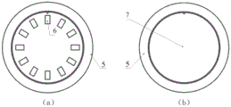
氧化镓晶片为圆形晶片7,其吸附在工作台的真空吸盘上或固定在工作台上,如图2(b)所示;The gallium oxide wafer is a
或,所述氧化镓晶片为周向均匀分布在圆盘上的多个小尺寸氧化镓晶片6,所述圆盘吸附在工作台的真空吸盘上或固定在工作台上,如图2(a)所示;Or, the gallium oxide wafer is a plurality of small-sized gallium oxide wafers 6 evenly distributed on the disk in the circumferential direction, and the disk is adsorbed on the vacuum suction cup of the worktable or fixed on the worktable, as shown in Figure 2 (a ) shown;
所述粗磨削、所述无进给磨削和所述精磨削过程中均通过冷却液冷却,冷却液的流量为4-6L/min,冷却液为去离子水。The rough grinding, the non-feed grinding and the fine grinding are all cooled by cooling liquid, the flow rate of the cooling liquid is 4-6 L/min, and the cooling liquid is deionized water.
所述步骤S2中,所述粗粒度金刚石砂轮的转速为600-1000r/min,转速方向为顺时针;In the step S2, the rotational speed of the coarse-grained diamond grinding wheel is 600-1000 r/min, and the rotational speed direction is clockwise;
所述工作台的转速200-400r/min,转速方向为逆时针。The rotational speed of the worktable is 200-400 r/min, and the rotational speed direction is counterclockwise.
所述步骤S3中,将粗粒度金刚石砂轮进给至氧化镓晶片上方,直至力传感器出现示值后停止进给的具体步骤如下:In the step S3, the coarse-grained diamond grinding wheel is fed to the top of the gallium oxide wafer, and the specific steps of stopping feeding until the force sensor shows a value are as follows:
将粗粒度金刚石砂轮进给至接近氧化镓晶片上方,之后,以10μm/min的进给速度缓慢向氧化镓晶片进给,直至力传感器出现示值后停止进给;Feed the coarse-grained diamond grinding wheel close to the top of the gallium oxide wafer, and then slowly feed it to the gallium oxide wafer at a feed speed of 10 μm/min, until the force sensor shows a value and stop feeding;
所述步骤S3中,所述初始进给速度为0.5-1μm/min,所述最大磨削力F粗为20-30N,所述进给量为10-20μm;In the step S3, the initial feed rate is 0.5-1 μm/min, the maximum grinding force F is roughly 20-30 N, and the feed amount is 10-20 μm;
所述步骤S3中,通过负反馈系统保证粗磨削过程中磨削力在F粗±0.1N的范围内波动;In the step S3, the negative feedback system is used to ensure that the grinding force fluctuates within the range of F rough ±0.1N during the rough grinding process;
数据处理器实时采集力传感器测得的磨削力信号,并放大处理输送给所述负反馈系统,所述负反馈系统将其与设定的最大磨削力进行比较,不断地反馈给控制系统控制粗粒度金刚石砂轮进给速度,进给速度的增减程度与所受实时磨削力与设定的最大磨削力的差值相关,如图3中流程图所示,m与V n 、V m 呈一定关系,以保证粗磨削过程中磨削力在F 粗±0.1N的范围内波动;The data processor collects the grinding force signal measured by the force sensor in real time, and amplifies it and sends it to the negative feedback system. The negative feedback system compares it with the set maximum grinding force and continuously feeds it back to the control system. Control the feed speed of the coarse-grained diamond grinding wheel. The increase or decrease of the feed speed is related to the difference between the real-time grinding force and the set maximum grinding force. As shown in the flowchart in Figure 3, m and V n , V m has a certain relationship to ensure that the grinding force fluctuates within the range of F rough ± 0.1N during rough grinding;
所述粗粒度金刚石砂轮的磨料粒度大小为W10-W14。The abrasive grain size of the coarse-grained diamond grinding wheel is W10-W14.
粗磨削过程中利用数据处理器,分析磨削力数据,并反馈控制粗粒度金刚石砂轮进给速度,不断地控制其最大磨削力,使其在一定波动范围(F 粗±0.1N)内实现恒力磨削,以控制氧化镓晶体发生解理的概率。During the rough grinding process, the data processor is used to analyze the grinding force data, and feedback control the feed rate of the coarse-grained diamond grinding wheel, and continuously control the maximum grinding force to keep it within a certain fluctuation range ( F coarse ±0.1N). Achieve constant force grinding to control the probability of cleavage of gallium oxide crystals.
所述无进给磨削的参数除进给速度为零外,其余参数和所述粗磨削参数一致;The parameters of the no-feed grinding are the same as the parameters of the rough grinding except the feed speed is zero;
所述无进给磨削的磨削时间为3min。The grinding time of the no-feed grinding was 3 min.
所述无进给磨削的目的是为了消除由于进刀时产生的弹性变形及其让刀量,提高表面光洁度,为精磨削做准备。The purpose of the no-feed grinding is to eliminate the elastic deformation caused by the feeding and the amount of the knife, improve the surface finish, and prepare for fine grinding.
所述步骤S5中,所述细粒度金刚石砂轮的转速为1000-2400r/min,转速方向为顺时针;In the step S5, the rotational speed of the fine-grained diamond grinding wheel is 1000-2400 r/min, and the rotational speed direction is clockwise;
所述工作台的转速300-400r/min,转速方向为逆时针。The rotational speed of the worktable is 300-400 r/min, and the rotational speed direction is counterclockwise.
所述步骤S6中,将细粒度金刚石砂轮进给至无进给磨削后的氧化镓晶片上方,直至力传感器出现示值后停止进给的具体步骤如下:In the step S6, the fine-grained diamond grinding wheel is fed to the top of the gallium oxide wafer after no-feed grinding, and the specific steps of stopping feeding until the force sensor shows a value are as follows:
将细粒度金刚石砂轮进给至接近无进给磨削后的氧化镓晶片上方,之后,以10μm/min的进给速度缓慢向氧化镓晶片进给,直至力传感器出现示值后停止进给;Feed the fine-grained diamond grinding wheel close to the top of the gallium oxide wafer after no-feed grinding, and then slowly feed it to the gallium oxide wafer at a feed rate of 10 μm/min until the force sensor shows a value and stops feeding;
所述步骤S6中,所述初始进给速度为0.5-1μm/min,所述最大磨削力F细为30-60N,所述进给量为5-10μm;In the step S6, the initial feed rate is 0.5-1 μm/min, the maximum grinding force F is 30-60 N, and the feed amount is 5-10 μm;
所述步骤S6中,通过负反馈系统保证精磨削过程中磨削力在F细±0.1N的范围内波动;In the step S6, the negative feedback system is used to ensure that the grinding force fluctuates within the range of F fine ±0.1N during the fine grinding process;
数据处理器实时采集力传感器测得的磨削力信号,并放大处理输送给所述负反馈系统,所述负反馈系统将其与设定的最大磨削力进行比较,不断地反馈给控制系统控制细粒度金刚石砂轮进给速度,进给速度的增减程度与所受实时磨削力与设定的最大磨削力的差值相关如图3中流程图所示,m与Vn、Vm呈一定关系,以保证精磨削过程中磨削力在F细±0.1N的范围内波动;The data processor collects the grinding force signal measured by the force sensor in real time, and amplifies it and sends it to the negative feedback system. The negative feedback system compares it with the set maximum grinding force and continuously feeds it back to the control system. Control the feed speed of the fine-grained diamond grinding wheel. The increase or decrease of the feed speed is related to the difference between the real-time grinding force and the set maximum grinding force. As shown in the flow chart in Figure 3, m and Vn, Vm A certain relationship is required to ensure that the grinding force fluctuates within the range of F fine ±0.1N during the fine grinding process;
所述细粒度金刚石砂轮的磨料粒度大小为W1-W5。The abrasive grain size of the fine-grained diamond grinding wheel is W1-W5.
精磨削过程中利用数据处理器,分析磨削力数据,并反馈控制细粒度金刚石砂轮进给速度,不断地控制其最大磨削力,使其在一定波动范围(F细±0.1N)内实现恒力磨削,以控制氧化镓晶体发生解理的概率。During the fine grinding process, the data processor is used to analyze the grinding force data, and the feed rate of the fine-grained diamond grinding wheel is fed back and controlled, and the maximum grinding force is continuously controlled to keep it within a certain fluctuation range (F fine ±0.1N). Achieve constant force grinding to control the probability of cleavage of gallium oxide crystals.
与现有技术相比,本发明的有益效果是:Compared with the prior art, the beneficial effects of the present invention are:
本发明基于力传感器的反馈来控制进给速度以控制磨削力,同时采用细粒度金刚石砂轮的超精密加工方法,有效的解决了氧化镓在机械加工阶段,尤其是磨削阶段出现的解理问题,并且细粒度的磨粒可降低损伤层的损伤程度和损伤厚度,缩短了后续的化学机械抛光工序的时间和减少了其去除量。The invention controls the feed speed based on the feedback of the force sensor to control the grinding force, and at the same time adopts the ultra-precision machining method of the fine-grained diamond grinding wheel, which effectively solves the cleavage of gallium oxide in the machining stage, especially the grinding stage. In addition, the fine-grained abrasive particles can reduce the damage degree and thickness of the damaged layer, shorten the time of the subsequent chemical mechanical polishing process and reduce its removal amount.
负反馈系统实时接收由数据处理器采集并放大的力传感器测得的磨削力的信号,不断地反馈给控制系统对进给速度实时控制以实现磨削力小于氧化镓解理应力阈值,解决了氧化镓机械加工中易出现的解离现象,提高了氧化镓晶体表面质量,实现了高成品率。The negative feedback system receives the grinding force signal measured by the force sensor collected and amplified by the data processor in real time, and continuously feeds it back to the control system to control the feed speed in real time, so as to realize that the grinding force is less than the cleavage stress threshold of gallium oxide. The dissociation phenomenon that is easy to occur in the machining of gallium oxide is eliminated, the surface quality of the gallium oxide crystal is improved, and a high yield is achieved.
基于上述理由本发明可在硬脆半导体晶片超精密加工等领域广泛推广。Based on the above reasons, the present invention can be widely promoted in the fields of ultra-precision machining of hard and brittle semiconductor wafers.
附图说明Description of drawings
为了更清楚地说明本发明实施例或现有技术中的技术方案,下面将对实施例或现有技术描述中所需要使用的附图做以简单地介绍,显而易见地,下面描述中的附图是本发明的一些实施例,对于本领域普通技术人员来讲,在不付出创造性劳动性的前提下,还可以根据这些附图获得其他的附图。In order to illustrate the embodiments of the present invention or the technical solutions in the prior art more clearly, the following briefly introduces the accompanying drawings that need to be used in the description of the embodiments or the prior art. Obviously, the accompanying drawings in the following description These are some embodiments of the present invention. For those of ordinary skill in the art, other drawings can also be obtained based on these drawings without any creative effort.
图1为本发明的具体实施方式中易解理半导体晶体的加工方法的防解理示意图。FIG. 1 is a schematic diagram of preventing cleavage of a method for processing an easily cleavable semiconductor crystal according to an embodiment of the present invention.
图2(a)为本发明的小尺寸氧化镓晶片固定圆盘在工作台上的布置示意图;图2(b)为本发明的圆形晶片在工作台上的布置示意图。Figure 2 (a) is a schematic diagram of the arrangement of the small-sized gallium oxide wafer fixing disk on the worktable of the present invention; Figure 2 (b) is a schematic diagram of the arrangement of the circular wafer of the present invention on the worktable.
图3为本发明的控制系统流程图。FIG. 3 is a flow chart of the control system of the present invention.
图中:1为金刚石砂轮;2为氧化镓晶片;3为真空吸盘;4为力传感器;5为工作台;6为小尺寸氧化镓晶片;7为圆形晶片;In the figure: 1 is a diamond grinding wheel; 2 is a gallium oxide wafer; 3 is a vacuum chuck; 4 is a force sensor; 5 is a workbench; 6 is a small-sized gallium oxide wafer; 7 is a circular wafer;
具体实施方式Detailed ways
为使本发明实施例的目的、技术方案和优点更加清楚,下面将结合本发明实施例中的附图,对本发明实施例中的技术方案进行清楚、完整地描述,显然,所描述的实施例是本发明一部分实施例,而不是全部的实施例。基于本发明中的实施例,本领域普通技术人员在没有做出创造性劳动前提下所获得的所有其他实施例,都属于本发明保护的范围。In order to make the purposes, technical solutions and advantages of the embodiments of the present invention clearer, the technical solutions in the embodiments of the present invention will be clearly and completely described below with reference to the accompanying drawings in the embodiments of the present invention. Obviously, the described embodiments These are some embodiments of the present invention, but not all embodiments. Based on the embodiments of the present invention, all other embodiments obtained by those of ordinary skill in the art without creative efforts shall fall within the protection scope of the present invention.
如图1所示,一种易解理半导体晶体的加工方法,具有如下步骤:As shown in Fig. 1, a processing method of easily cleavable semiconductor crystal has the following steps:
S1、打开超精密磨床,将一片切割后的2英寸的氧化镓晶片2吸附在超精密磨床的工作台5上的真空吸盘3上,安装工件上的位置如图2(b)所示,装夹氧化镓晶片2时,使工作台5的中心与氧化镓晶片2的中心重合;S1. Turn on the ultra-precision grinder, and adsorb a cut 2-inch gallium oxide wafer 2 on the
S2、使用粗粒度金刚石砂轮1,所述粗粒度金刚石砂轮1的磨料粒度大小为W10-W14,将粗粒度金刚石砂轮1的磨料层端面调整到工作台5的中心位置,然后打开冷却液,冷却液为去离子水,冷却液流量为4-6L/min;然后启动粗粒度金刚石砂轮1,其转速为600-1000r/min,转速方向为顺时针;然后启动工作台5,工作台5转速为200-400r/min,转速方向为逆时针;S2, use the coarse-grained
S3、打开力传感器4,将粗粒度金刚石砂轮1手动进给至氧化镓晶片2上方1mm处,打开自动进给,进给速度为10μm/min,直至力传感器4出现示值后关掉自动进给,然后打开负反馈系统,同时设定粗磨削的初始进给速度Vi为0.5μm/min,最大磨削力F粗为30N,进给量为20μm,之后,对氧化镓晶片2进行粗磨削直至达到设定进给量,粗磨削过程中所述负反馈系统实时接收由数据处理器采集并放大的所述力传感器4测得的磨削力的信号,不断地反馈给控制系统控制粗粒度金刚石砂轮1进给速度,以保证粗磨削过程中磨削力在F粗±0.1N的范围内波动,如图3所示,以控制氧化镓晶体发生解理的概率。粗磨削后,进行3min无进给磨削,为下一步精磨削做准备;S3. Turn on the force sensor 4, manually feed the coarse-grained
S4、抬起粗粒度金刚石砂轮1,并停止粗粒度金刚石砂轮1和工作台5旋转,将粗粒度金刚石砂轮1更换成细粒度金刚石砂轮1,所述细粒度金刚石砂轮1的的磨料粒度大小为W1-W5,将细粒度金刚石砂轮1的磨料层端面调整到工作台5的中心位置,然后打开冷却液,冷却液为去离子水,冷却液流量为4-6/min;然后启动细粒度金刚石砂轮1,其转速为1000-2400r/min,转速方向为顺时针;然后启动工作台5,工作台5转速为300-400r/min,转速方向为逆时针;S4, lift the coarse-grained
S5、打开力传感器4,将细粒度金刚石砂轮1手动进给至无进给磨削后的氧化镓晶片2上方1mm处,打开自动进给,进给速度为10μm/min,直至力传感器4出现示值后关掉自动进给,然后打开负反馈系统,同时设定精磨削的初始进给速度Vi为0.5μm/min,最大磨削力F细为60N,进给量为10μm,之后,对氧化镓晶片2进行精磨削直至达到设定进给量,精磨削过程中所述负反馈系统实时接收由数据处理器采集并放大的所述力传感器4测得的磨削力的信号,不断地反馈给控制系统控制细粒度金刚石砂轮1进给速度,以保证精磨削过程中磨削力在F细±0.1N的范围内波动,如图3所示,以控制氧化镓晶体发生解理的概率,实现低于解理磨削力的超精密磨削;S5. Turn on the force sensor 4, manually feed the fine-grained
精磨削结束后,可将氧化镓晶片2取下,进行清洗,氧化镓晶片2的超精密磨削加工完成。最终测量,得到的氧化镓晶片2的Ra≤1nm,TTV≤5μm。After finishing the fine grinding, the gallium oxide wafer 2 can be removed and cleaned, and the ultra-precision grinding process of the gallium oxide wafer 2 is completed. In the final measurement, Ra≤1 nm and TTV≤5 μm of the obtained gallium oxide wafer 2 .
最后应说明的是:以上各实施例仅用以说明本发明的技术方案,而非对其限制;尽管参照前述各实施例对本发明进行了详细的说明,本领域的普通技术人员应当理解:其依然可以对前述各实施例所记载的技术方案进行修改,或者对其中部分或者全部技术特征进行等同替换;而这些修改或者替换,并不使相应技术方案的本质脱离本发明各实施例技术方案的范围。Finally, it should be noted that the above embodiments are only used to illustrate the technical solutions of the present invention, but not to limit them; although the present invention has been described in detail with reference to the foregoing embodiments, those of ordinary skill in the art should understand that: The technical solutions described in the foregoing embodiments can still be modified, or some or all of the technical features thereof can be equivalently replaced; and these modifications or replacements do not make the essence of the corresponding technical solutions deviate from the technical solutions of the embodiments of the present invention. scope.
Claims (5)
Priority Applications (1)
| Application Number | Priority Date | Filing Date | Title |
|---|---|---|---|
| CN201910867396.2A CN110640552B (en) | 2019-09-12 | 2019-09-12 | Processing method of easily-cleaved semiconductor crystal |
Applications Claiming Priority (1)
| Application Number | Priority Date | Filing Date | Title |
|---|---|---|---|
| CN201910867396.2A CN110640552B (en) | 2019-09-12 | 2019-09-12 | Processing method of easily-cleaved semiconductor crystal |
Publications (2)
| Publication Number | Publication Date |
|---|---|
| CN110640552A CN110640552A (en) | 2020-01-03 |
| CN110640552B true CN110640552B (en) | 2020-11-06 |
Family
ID=68991855
Family Applications (1)
| Application Number | Title | Priority Date | Filing Date |
|---|---|---|---|
| CN201910867396.2A Active CN110640552B (en) | 2019-09-12 | 2019-09-12 | Processing method of easily-cleaved semiconductor crystal |
Country Status (1)
| Country | Link |
|---|---|
| CN (1) | CN110640552B (en) |
Families Citing this family (5)
| Publication number | Priority date | Publication date | Assignee | Title |
|---|---|---|---|---|
| CN115091287B (en) * | 2022-07-15 | 2023-12-29 | 华海清科股份有限公司 | Ultra-precise grinding parameter adjustment method and grinding system |
| CN116021398B (en) * | 2023-02-17 | 2026-04-07 | 上海迈铸半导体科技有限公司 | A semiconductor grinding structure and apparatus |
| CN116021358A (en) * | 2023-03-28 | 2023-04-28 | 之江实验室 | A device and method for fine processing lithium niobate piezoelectric single crystal |
| CN117969356B (en) * | 2024-04-01 | 2024-06-25 | 陕西天成航空材料股份有限公司 | Detection method and detection device for average grain size of titanium alloy |
| CN120095705A (en) * | 2025-04-28 | 2025-06-06 | 河北同光半导体股份有限公司 | Chemical mechanical grinding method and device for semiconductor wafer |
Citations (9)
| Publication number | Priority date | Publication date | Assignee | Title |
|---|---|---|---|---|
| CN1887528A (en) * | 2006-07-17 | 2007-01-03 | 天津大学 | Constant micro force micro feeder for super pricise grinding of hard brittle material and its control method |
| CN101673668A (en) * | 2009-10-19 | 2010-03-17 | 中国电子科技集团公司第四十六研究所 | Method for polishing gallium nitride crystals |
| CN101716747A (en) * | 2009-11-18 | 2010-06-02 | 大连理工大学 | Piezoelectric type grinding force measuring device for ultraprecise grinding machine of silicon wafer |
| CN102009387A (en) * | 2010-11-20 | 2011-04-13 | 大连理工大学 | Semiconductor wafer grinding force on-line measurement device and force-controlling grinding method |
| CN204893721U (en) * | 2015-07-28 | 2015-12-23 | 安徽工程大学 | Silicon chip grinding force dynamic signal detection device |
| CN105563329A (en) * | 2015-12-16 | 2016-05-11 | 威海华东数控股份有限公司 | Self-adaptive grinding force control system for numerically-controlled grinding machine |
| CN106695478A (en) * | 2016-12-08 | 2017-05-24 | 中国电子科技集团公司第四十六研究所 | Cleavage-preventing processing method for gallium oxide crystals |
| CN206373778U (en) * | 2016-12-14 | 2017-08-04 | 洛阳理工学院 | A kind of feed speed adaptive control system based on grinding force |
| CN109333360A (en) * | 2018-10-15 | 2019-02-15 | 北京工业大学 | Device and method for on-line measurement of wafer thinning grinding force |
-
2019
- 2019-09-12 CN CN201910867396.2A patent/CN110640552B/en active Active
Patent Citations (9)
| Publication number | Priority date | Publication date | Assignee | Title |
|---|---|---|---|---|
| CN1887528A (en) * | 2006-07-17 | 2007-01-03 | 天津大学 | Constant micro force micro feeder for super pricise grinding of hard brittle material and its control method |
| CN101673668A (en) * | 2009-10-19 | 2010-03-17 | 中国电子科技集团公司第四十六研究所 | Method for polishing gallium nitride crystals |
| CN101716747A (en) * | 2009-11-18 | 2010-06-02 | 大连理工大学 | Piezoelectric type grinding force measuring device for ultraprecise grinding machine of silicon wafer |
| CN102009387A (en) * | 2010-11-20 | 2011-04-13 | 大连理工大学 | Semiconductor wafer grinding force on-line measurement device and force-controlling grinding method |
| CN204893721U (en) * | 2015-07-28 | 2015-12-23 | 安徽工程大学 | Silicon chip grinding force dynamic signal detection device |
| CN105563329A (en) * | 2015-12-16 | 2016-05-11 | 威海华东数控股份有限公司 | Self-adaptive grinding force control system for numerically-controlled grinding machine |
| CN106695478A (en) * | 2016-12-08 | 2017-05-24 | 中国电子科技集团公司第四十六研究所 | Cleavage-preventing processing method for gallium oxide crystals |
| CN206373778U (en) * | 2016-12-14 | 2017-08-04 | 洛阳理工学院 | A kind of feed speed adaptive control system based on grinding force |
| CN109333360A (en) * | 2018-10-15 | 2019-02-15 | 北京工业大学 | Device and method for on-line measurement of wafer thinning grinding force |
Non-Patent Citations (2)
| Title |
|---|
| 晶片减薄技术原理概况;柳滨;《电子工业专用设备》;20050615(第06期);全文 * |
| 树脂结合剂金刚石砂轮精密磨削单晶硅片的磨削力研究;林培勇等;《金刚石与磨料磨具工程》;20120820(第04期);全文 * |
Also Published As
| Publication number | Publication date |
|---|---|
| CN110640552A (en) | 2020-01-03 |
Similar Documents
| Publication | Publication Date | Title |
|---|---|---|
| CN110640552B (en) | Processing method of easily-cleaved semiconductor crystal | |
| CN102107391B (en) | A kind of processing method of SiC single crystal wafer | |
| CN104813439B (en) | Flat sic semiconductor substrate | |
| US7867059B2 (en) | Semiconductor wafer, apparatus and process for producing the semiconductor wafer | |
| CN101673668B (en) | Method for polishing gallium nitride crystals | |
| CN113206007B (en) | Preparation method of indium phosphide substrate | |
| CN100435288C (en) | Method for manufacturing silicon wafers | |
| TW202028547A (en) | High-flatness, low-damage and large-diameter monocrystalline silicon carbide substrate, and manufacturing method therefor | |
| CN110640565B (en) | Gallium oxide anti-cleavage processing method based on control force | |
| CN111630213A (en) | Seed crystal for single crystal 4H-SiC growth and its processing method | |
| CN105313234A (en) | Processing method for double-sided polished sapphire wafers | |
| CN103862354B (en) | The processing method of ultra thin single crystalline germanium wafer | |
| JP2019166598A (en) | Wafer chamfering device and wafer chamfering method | |
| CN110010458B (en) | Method for controlling surface morphology of semiconductor wafer and semiconductor wafer | |
| CN103681298A (en) | Machining method for high-yield monocrystalline silicon wafer for IGBT | |
| CN106695478B (en) | A kind of anti-cleavage processing method for gallium oxide crystal | |
| JP2010021394A (en) | Method of manufacturing semiconductor wafer | |
| CN115723027B (en) | A processing technology for subsurface damage-free gallium nitride wafer | |
| JP6032087B2 (en) | Method for producing group 13 nitride crystal substrate | |
| JP4283088B2 (en) | Workpiece surface processing method | |
| JP2010153844A (en) | Method of producing wafer for active layer | |
| KR101086966B1 (en) | Semiconductor Wafer Polishing Method | |
| TWI874254B (en) | Indium phosphide substrate and semiconductor epitaxial wafer | |
| JP4154683B2 (en) | Manufacturing method of high flatness back surface satin wafer and surface grinding back surface lapping apparatus used in the manufacturing method | |
| JP2025080129A (en) | Indium phosphide substrates and semiconductor epitaxial wafers |
Legal Events
| Date | Code | Title | Description |
|---|---|---|---|
| PB01 | Publication | ||
| PB01 | Publication | ||
| SE01 | Entry into force of request for substantive examination | ||
| SE01 | Entry into force of request for substantive examination | ||
| GR01 | Patent grant | ||
| GR01 | Patent grant |