CN110572011B - IGBT drive circuit soft switching device with short-circuit protection - Google Patents
IGBT drive circuit soft switching device with short-circuit protection Download PDFInfo
- Publication number
- CN110572011B CN110572011B CN201910768054.5A CN201910768054A CN110572011B CN 110572011 B CN110572011 B CN 110572011B CN 201910768054 A CN201910768054 A CN 201910768054A CN 110572011 B CN110572011 B CN 110572011B
- Authority
- CN
- China
- Prior art keywords
- module
- circuit
- type mos
- igbt chip
- resistor
- Prior art date
- Legal status (The legal status is an assumption and is not a legal conclusion. Google has not performed a legal analysis and makes no representation as to the accuracy of the status listed.)
- Active
Links
Images


Classifications
-
- G—PHYSICS
- G01—MEASURING; TESTING
- G01R—MEASURING ELECTRIC VARIABLES; MEASURING MAGNETIC VARIABLES
- G01R1/00—Details of instruments or arrangements of the types included in groups G01R5/00 - G01R13/00 and G01R31/00
- G01R1/30—Structural combination of electric measuring instruments with basic electronic circuits, e.g. with amplifier
-
- G—PHYSICS
- G01—MEASURING; TESTING
- G01R—MEASURING ELECTRIC VARIABLES; MEASURING MAGNETIC VARIABLES
- G01R1/00—Details of instruments or arrangements of the types included in groups G01R5/00 - G01R13/00 and G01R31/00
- G01R1/36—Overload-protection arrangements or circuits for electric measuring instruments
-
- H—ELECTRICITY
- H02—GENERATION; CONVERSION OR DISTRIBUTION OF ELECTRIC POWER
- H02M—APPARATUS FOR CONVERSION BETWEEN AC AND AC, BETWEEN AC AND DC, OR BETWEEN DC AND DC, AND FOR USE WITH MAINS OR SIMILAR POWER SUPPLY SYSTEMS; CONVERSION OF DC OR AC INPUT POWER INTO SURGE OUTPUT POWER; CONTROL OR REGULATION THEREOF
- H02M1/00—Details of apparatus for conversion
- H02M1/08—Circuits specially adapted for the generation of control voltages for semiconductor devices incorporated in static converters
-
- H—ELECTRICITY
- H03—ELECTRONIC CIRCUITRY
- H03K—PULSE TECHNIQUE
- H03K17/00—Electronic switching or gating, i.e. not by contact-making and –breaking
- H03K17/08—Modifications for protecting switching circuit against overcurrent or overvoltage
- H03K17/082—Modifications for protecting switching circuit against overcurrent or overvoltage by feedback from the output to the control circuit
- H03K17/0826—Modifications for protecting switching circuit against overcurrent or overvoltage by feedback from the output to the control circuit in bipolar transistor switches
-
- H—ELECTRICITY
- H03—ELECTRONIC CIRCUITRY
- H03K—PULSE TECHNIQUE
- H03K17/00—Electronic switching or gating, i.e. not by contact-making and –breaking
- H03K17/51—Electronic switching or gating, i.e. not by contact-making and –breaking characterised by the components used
- H03K17/56—Electronic switching or gating, i.e. not by contact-making and –breaking characterised by the components used by the use, as active elements, of semiconductor devices
- H03K17/567—Circuits characterised by the use of more than one type of semiconductor device, e.g. BIMOS, composite devices such as IGBT
-
- Y—GENERAL TAGGING OF NEW TECHNOLOGICAL DEVELOPMENTS; GENERAL TAGGING OF CROSS-SECTIONAL TECHNOLOGIES SPANNING OVER SEVERAL SECTIONS OF THE IPC; TECHNICAL SUBJECTS COVERED BY FORMER USPC CROSS-REFERENCE ART COLLECTIONS [XRACs] AND DIGESTS
- Y02—TECHNOLOGIES OR APPLICATIONS FOR MITIGATION OR ADAPTATION AGAINST CLIMATE CHANGE
- Y02B—CLIMATE CHANGE MITIGATION TECHNOLOGIES RELATED TO BUILDINGS, e.g. HOUSING, HOUSE APPLIANCES OR RELATED END-USER APPLICATIONS
- Y02B70/00—Technologies for an efficient end-user side electric power management and consumption
- Y02B70/10—Technologies improving the efficiency by using switched-mode power supplies [SMPS], i.e. efficient power electronics conversion e.g. power factor correction or reduction of losses in power supplies or efficient standby modes
Abstract
The soft switching device with the short-circuit protection function for the IGBT driving circuit comprises a driving control module (A01), a driving power module (A02), a voltage comparison module (A03), a switching circuit module (A04) and an IGBT chip module (A05). The invention takes the induced electromotive force on the emitter parasitic inductance of the IGBT chip module as a feedback signal to control different stages of the switching-on and switching-off processes to access different resistance resistors so as to realize IGBT soft switching, judges whether the switching-off process is short-circuited or not through the feedback signal, and protects the IGBT through the active clamping technology.
Description
Technical Field
The invention relates to the integrated electronic circuit technology, in particular to an IGBT drive circuit soft switching device with short-circuit protection.
Background
Insulated Gate Bipolar Transistor (IGBT) is a novel device composed of an Insulated Gate field effect Transistor (MOS) and a Bipolar Transistor (BJT), effectively combining the advantages of the MOS and the BJT, and is widely used in the conventional and emerging fields such as the automotive industry, high-speed railways, and electrical fields. The driving circuit influences the working performance of the IGBT module, can effectively control the IGBT switch off time, reduce the switch loss, suppress voltage and current spikes, prevent the latching effect, and monitor and protect various faults which may be met by the IGBT in the working process, thereby ensuring that the IGBT works in a safe working area. In the aspect of the existing IGBT driving circuit, a gate resistor with a fixed resistance value is adopted to switch on and off the IGBT. According to the switching characteristics of the IGBT, the gate resistor with the large resistance value can effectively control the voltage and current peak of the collector and prevent the latch up effect, but the gate resistor with the large resistance value can slow down the charge and discharge rate of the gate, prolong the turn-on and turn-off time of the IGBT and increase the switching loss; conversely, the adoption of a smaller gate resistance can cause the voltage of a collector and the current peak to be too high, but can accelerate the charge-discharge rate of the gate, improve the switching-off speed and reduce the switching loss. In addition, the existing driving circuit cannot well monitor and solve the short-circuit condition of the IGBT, so that the existing IGBT driving circuit is low in switching performance, short in service life, incapable of effectively and accurately monitoring short-circuit faults and low in reliability. Based on the current industrial situation, a brand-new IGBT driving circuit is needed to be invented to improve the switching characteristic of the IGBT, monitor and process the short circuit situation, prolong the service life and improve the reliability.
Disclosure of Invention
The invention aims to solve the technical problem of overcoming the defects in the prior art and provides the IGBT driving circuit soft switching device with short-circuit protection, which can effectively monitor short-circuit faults and has high reliability and long service life.
The technical scheme adopted by the invention for solving the technical problems is as follows:
the IGBT driving circuit soft switching device with short-circuit protection comprises a driving control module, a driving power module, a voltage comparison module, a switching circuit module and an IGBT chip module.
The output end of the drive control module is connected with the input end of the drive power module, the drive control module is used for providing PWM pulse signals for the drive power module, and the on-off of a switching tube in the drive power module is controlled through the PWM pulse signals, so that the on-off of an IGBT chip is realized;
the output end of the driving power module is connected with the input end of the switch circuit module, and the driving power module outputs a switching-on or switching-off voltage to the switch circuit module and plays a role in isolating a driving signal, so that a basis is provided for switching on or off the gate pole of the IGBT chip module;
the output end of the voltage comparison module is connected with the other input end of the switch circuit module, and the feedback signal sent by the IGBT chip module is judged by the voltage comparison module and then provides a high-low level signal for the switch circuit module;
the switching circuit module selects and turns on the corresponding MOS switching tube in the switching circuit module by using the high-low level signal transmitted by the voltage comparison module, so that the on-off voltage output by the driving power module is added to the gate pole small resistor and the gate pole large resistor A045 active clamping resistor connected with the corresponding MOS switching tube in the switching circuit module;
the IGBT chip module adopts an IGBT chip (such as an England flying FZ1500R33HE3 type chip), an emitter of the IGBT chip module is connected with the input end of the voltage comparison module, a gate pole small resistor, a gate pole large resistor and an active clamping resistor in the switch circuit module are all connected with a gate pole of the IGBT chip module, the emitter of the IGBT chip module is connected with a parasitic inductor in series, induced electromotive force on the parasitic inductor is used as a feedback signal to be connected to the input end of the voltage comparison module, and the IGBT chip module is an application carrier of the invention.
Further, the driving power module comprises a push-pull conversion circuit and a voltage stabilizing circuit; the output end of the push-pull conversion circuit is connected with the input end of the voltage stabilizing circuit, the push-pull conversion circuit controls the conduction of a switch tube in the push-pull conversion circuit according to a PWM pulse signal of the drive control module, so that the input voltage of the switch tube in the push-pull conversion circuit is converted into a chopping wave signal, the chopping wave signal is transmitted to a secondary side of a transformer through a primary side of the transformer in the push-pull conversion circuit, the secondary side of the transformer is connected to the voltage stabilizing circuit, and the voltage stabilizing circuit converts the chopping wave signal into the on or off voltage of the IGBT and transmits.
Further, the voltage comparison module comprises a primary voltage comparator, a secondary voltage comparator, a primary direct-current voltage source and resistor series structure, a secondary direct-current voltage source and resistor series structure and an N-type MOS switching tube, wherein the input end of the primary voltage comparator and the source electrode of the N-type MOS switching tube are connected with the emitter electrode of the IGBT chip module, the output end of the primary voltage comparator is connected with the grid electrode of the N-type MOS switching tube, the drain electrode of the N-type MOS switching tube is connected with the input end of the secondary voltage comparator, the primary direct-current voltage source and resistor series structure is connected with the other input end of the primary voltage comparator, and the secondary direct-current voltage source and resistor series structure is connected with the other input end of the secondary voltage comparator; the output end of the primary voltage comparator and the output end of the secondary voltage comparator are connected with the input end of the switch circuit module.
The model of each of the primary voltage comparator and the secondary voltage comparator is LM339, induced electromotive force of parasitic inductance of an emitter of the IGBT chip is used as a feedback signal to be transmitted to the primary voltage comparator, the primary voltage comparator provides short-circuit reference voltage through a primary direct-current voltage source and a resistor series structure, the primary voltage comparator outputs high level or low level to the switch circuit module after comparing and judging the feedback signal transmitted by the IGBT chip, the feedback signal transmitted by the IGBT chip is transmitted to the secondary voltage comparator through an N-type MOS switch tube, the secondary voltage comparator provides normal operation reference voltage through a secondary direct-current voltage source and a resistor series structure, and the secondary voltage comparator outputs high level or low level to the switch circuit module after comparing and judging the feedback signal.
Further, the switch circuit module comprises an N-type MOS switch tube, two P-type MOS switch tubes, a gate pole small circuit, a gate pole large resistor and an active clamping resistor, wherein the N-type MOS switch tube and the two P-type MOS switch tubes of the switch circuit module are respectively used for connecting the gate pole small resistor, the gate pole large resistor and the active clamping resistor. The drains of the N-type MOS switching tubes are connected with the gate minimum resistor, the drains of the two P-type MOS switching tubes are respectively connected with the gate maximum circuit and the active clamping resistor, the gate small circuit and the gate large resistor are all connected with the gate of the IGBT chip module.
The switching circuit module further comprises another P-type MOS switching tube, the grid electrode of the other P-type MOS switching tube is connected with the output end of the primary voltage comparator, the source electrode of the other P-type MOS switching tube is connected with the collector electrode of the IGBT chip module, and the drain electrode of the other P-type MOS switching tube is connected with the gate electrode of the IGBT chip module.
The gate electrode small resistor and the gate electrode large resistor are used as gate electrode driving resistors of the IGBT chip module, and the active clamping resistor plays a role in short-circuit fault voltage stabilization.
If the IGBT chip module has a short-circuit fault, the collector current of the IGBT chip module rises to be more than 4 times of the rated current of the IGBT chip module within 3 mu s, the induced electromotive force of the parasitic inductance of the emitter of the IGBT chip module used as a feedback signal is larger than the short-circuit reference voltage provided by a primary voltage comparator through a primary direct-current voltage source and a resistor series structure, the output of the primary voltage comparator is at a low level, a P-type MOS switching tube connected with an active clamping resistor is switched on, a branch formed by connecting the P-type MOS switching tube with the active clamping resistor is switched on, meanwhile, the P-type MOS switching tube connected with the gate pole of the IGBT chip module is switched on, and compensation current is injected into the gate pole of the IGBT chip module through the P-type MOS switching tube to provide short-circuit protection; if the IGBT chip module normally operates, the induced electromotive force of the emitter parasitic inductance of the IGBT chip module is kept below a preset threshold value, the induced electromotive force of the emitter parasitic inductance of the IGBT chip module is smaller than a short-circuit reference voltage provided by a primary voltage comparator through a primary direct-current voltage source and a resistor series structure, and the primary voltage comparator outputs a high level, so that the primary voltage comparator transmits a feedback signal to a secondary voltage comparator through an N-type MOS switching tube connected with the primary voltage comparator; if the IGBT chip module is in a gate charging delay and Miller platform continuous stage in a switching-on process or in a switching-off delay and trailing current stage in a switching-off process, the change rate of collector current of the IGBT chip module is zero, so that induced electromotive force of emitter parasitic inductance of the IGBT chip module is zero, or the induced electromotive force of the emitter parasitic inductance of the IGBT chip module is smaller than normal operation reference voltage provided by a secondary voltage comparator through a secondary direct current voltage source and a resistor series structure, and the output of a secondary transformer is high level, an N-type MOS switching tube is switched on, and a branch formed by connecting the N-type MOS switching tube with a gate minimum resistor is switched on; if the IGBT chip module is in a current rising stage of a switching-on process or a voltage rising stage of a switching-off process, the collector current of the IGBT chip module rises to be more than 300A within 1 mu s, so that induced electromotive force of parasitic inductance of an emitter of the IGBT chip module is larger than normal operation reference voltage provided by a secondary voltage comparator through a secondary direct current voltage source and a resistor series structure, the output of a secondary transformer is low level, a P-type MOS switching tube is switched on, and a branch formed by connecting the P-type MOS switching tube with a maximum resistor is switched on.
The soft switching device of the IGBT driving circuit with short-circuit protection has the following specific functions:
(1) resistors with different resistance values can be selected and connected according to the IGBT switching characteristics, and the IGBT switching performance is improved;
(2) short-circuit faults in the turn-off state can be monitored and safely turned off, and damage to devices is prevented;
(3) the device has generality, and different IGBT chips can be adapted by changing element parameters.
The invention takes the induced electromotive force on the emitter parasitic inductance of the IGBT chip module as a feedback signal, controls different stages of the IGBT to access different resistance resistors so as to realize the IGBT soft switch, judges whether the turn-off process is short-circuited or not through the feedback signal, and protects the IGBT through an active clamping technology.
Drawings
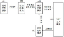
FIG. 1 is a block diagram of the overall architecture of the present invention;
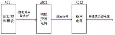
FIG. 2 is a block diagram of the drive power module architecture of the present invention;
FIG. 3 is a block diagram of the voltage comparison module architecture of the present invention;
FIG. 4 is a block diagram of the switching circuit module architecture of the present invention;
fig. 5 is a schematic circuit diagram of an example of the present invention.
Detailed Description
The present invention will be described in further detail with reference to the accompanying drawings.
Referring to fig. 1, the soft switching device with short-circuit protection for the IGBT driving circuit of the invention includes a driving control module a01, a driving power module a02, a voltage comparison module a03, a switching circuit module a04, and an IGBT chip module a 05.
The output end of the drive control module A01 is connected with the input end of the drive power module A02, and the drive control module A01 is used for providing a PWM pulse signal for the drive power module A02 and controlling the on and off of a switch tube in the drive power module A02 through the PWM pulse signal;
the output end of the driving power module A02 is connected with the input end of the switch circuit module A04, and the driving power module A02 outputs a turn-on or turn-off voltage to the switch circuit module A04 and plays a role in driving signal isolation, so that a basis is provided for the turn-on or turn-off of the gate pole of the IGBT chip module A05;
the output end of the voltage comparison module A03 is connected with the other input end of the switch circuit module A04, and a feedback signal sent by the IGBT chip module A05 is judged by the overvoltage comparison module A03 to provide a high-low level signal for the switch circuit module A04;
the switch circuit module A04 utilizes the high-low level signal transmitted by the voltage comparison module A03 to select and turn on the corresponding MOS switch tube in the switch circuit module A04, so that the on-off voltage output by the driving power module A02 is added to the gate pole small resistor A044, the gate pole large resistor A045 or the active clamping resistor A046 which are connected with the corresponding MOS switch tube in the switch circuit module A04;
the IGBT chip module A05 adopts an IGBT chip, an emitter of the IGBT chip module is connected with the input end of the voltage comparison module A03, a gate small resistor A044, a gate large resistor A045 and an active clamping resistor A046 in the switch circuit module A04 are all connected with a gate of the IGBT chip module, the emitter of the IGBT chip module is connected with a parasitic inductor in series, induced electromotive force on the parasitic inductor is used as a feedback signal to be connected to the input end of the voltage comparison module A03, and the IGBT chip module A05 is an application carrier of the invention.
Referring to fig. 2, the driving power module a02 includes a push-pull conversion circuit a021 and a voltage stabilizing circuit a 022; the output end of the push-pull conversion circuit A021 is connected with the input end of the voltage stabilizing circuit A022, the push-pull conversion circuit A021 controls the conduction of a switching tube in the push-pull conversion circuit A021 according to a PWM pulse signal of the drive control module A01, so that the input voltage of the switching tube in the push-pull conversion circuit A021 is converted into a chopping wave signal, the chopping wave signal is transmitted to the secondary side of a transformer through the primary side of the transformer in the push-pull conversion circuit A021, the secondary side of the transformer is connected to the voltage stabilizing circuit A022, and the voltage stabilizing circuit A022 converts the chopping wave signal into the on or off voltage of the IGBT and transmits the on or.
Without loss of generality, the push-pull conversion circuit A021 adopted by the invention is a typical push-pull conversion circuit and comprises two switching tubes and a transformer, collectors of the two switching tubes are respectively connected to the head end and the tail end of a primary coil of the transformer, and sources of the two switching tubes are both connected with the output end of the drive control module A01. The voltage stabilizing circuit A022 is composed of a voltage stabilizing tube and a capacitance filtering rectification circuit, the drive control module outputs PWM signals to control two switch tubes of the push-pull conversion circuit, input voltage of the push-pull conversion circuit is converted into chopping signals and then transmitted to a secondary side through a primary side of a transformer, and then the switching-on or switching-off voltage of the IGBT is output through the voltage stabilizing tube of the voltage stabilizing circuit A022 and the capacitance filtering rectification circuit.
Referring to fig. 3, the voltage comparison module a03 includes a primary voltage comparator a031, a secondary voltage comparator a033, a primary dc voltage source and resistor series structure a034, a secondary dc voltage source and resistor series structure a035, and an N-type MOS switch tube a032, wherein an input terminal of the primary voltage comparator a031 and a source terminal of the N-type MOS switch tube a032 are both connected to an emitter terminal of the IGBT chip module a05, an output terminal of the primary voltage comparator a031 is connected to a gate terminal of the N-type MOS switch tube a032, a drain terminal of the N-type MOS switch tube a032 is connected to an input terminal of the secondary voltage comparator a033, the primary dc voltage source and resistor series structure a034 is connected to another input terminal of the primary voltage comparator a031, and the secondary dc voltage source and series structure a035 are connected to another input terminal of the secondary voltage comparator a 033; the output end of the primary voltage comparator A031 and the output end of the secondary voltage comparator A033 are connected with the input end of the switch circuit module A04.
The primary voltage comparator A031 and the secondary voltage comparator A033 are used for comparing and judging feedback signals, the primary direct-current voltage source and resistor series structure A034 and the secondary direct-current voltage source and resistor series structure A035 are used for providing reference voltages, and the N-type MOS switching tube A032 transmits the feedback signals to the secondary voltage comparator A033.
Without loss of generality, the models adopted by the primary voltage comparator a031 and the secondary voltage comparator a033 are LM339, induced electromotive force of emitter parasitic inductance of the IGBT chip is transmitted to the primary voltage comparator a031 as a feedback signal, the primary voltage comparator a031 provides a short-circuit reference voltage through the primary direct-current voltage source and the resistor series structure a034, the primary voltage comparator a031 compares and judges the feedback signal transmitted by the IGBT chip and outputs a high level or a low level to the switch circuit module a04, the feedback signal transmitted by the IGBT chip is transmitted to the secondary voltage comparator a033 through the N-type MOS switch tube a032, the secondary voltage comparator a033 provides a normal operation reference voltage through the secondary direct-current voltage source and the resistor series structure a035, and the secondary voltage comparator a033 compares and judges the feedback signal and outputs a high level or a low level to the switch circuit module a 04.
Referring to fig. 4, the switching circuit module includes an N-type MOS switching tube a041, two P-type MOS switching tubes a042 and a043, a gate small resistor a044, a gate large resistor a045, and an active clamping resistor a046, and the N-type MOS switching tube a041, the P-type MOS switching tube a042, and the P-type MOS switching tube a043 of the switching circuit module are respectively used for connecting the gate small resistor a044, the gate large resistor a045, and the active clamping resistor a 046. The drain electrode of the N-type MOS switch tube A041 is connected with a minimum resistance A044, the drain electrode of the P-type MOS switch tube A042 is connected with a maximum circuit A045, the drain electrode of the P-type MOS switch tube A043 is connected with an active clamping resistance A046, and the active clamping resistance A046, the gate electrode small circuit A044 and the gate electrode large resistance A045 are all connected with the gate electrode of the IGBT chip module A05. The grid electrode of the N-type MOS switching tube A041 and the grid electrode of the P-type MOS switching tube A042 are both connected with the output end of a secondary voltage comparator A033, and the grid electrode of the P-type MOS switching tube A043 is connected with the output end of a primary voltage comparator A031. The source electrode of the N-type MOS switch tube A041, the source electrode of the P-type MOS switch tube A042 and the source electrode of the P-type MOS switch tube A043 are all connected with the output end of the voltage stabilizing circuit A022.
The switch circuit module further comprises a P-type MOS switch tube A047, the grid electrode of the P-type MOS switch tube A047 is connected with the output end of the primary voltage comparator A031, the source electrode of the P-type MOS switch tube A047 is connected with the collector electrode of the IGBT chip module A05, and the drain electrode of the P-type MOS switch tube A047 is connected with the gate electrode of the IGBT chip module A05.
The gate minimum resistor A044 and the gate large resistor A045 are used as gate driving resistors of the IGBT chip module A05, and the active clamping resistor A046 plays a role in short-circuit fault voltage stabilization.
Without loss of generality, if the output of the primary voltage comparator a031 is low level, the P-type MOS switch tube a043 in short-circuit fault mode is switched on, a branch formed by connecting the P-type MOS switch tube a043 and the active clamp resistor a046 is switched on, meanwhile, the P-type MOS switch tube a047 is switched on, and compensation current is injected to the gate of the IGBT chip module a05 through the P-type MOS switch tube a 047; if the output of the primary voltage comparator a031 is high level, the primary comparator a031 transmits a feedback signal to the secondary voltage comparator a033 through the N-type MOS switch tube a032, if the output of the secondary transformer a033 is high level, the branch formed by connecting the N-type MOS switch tube a041 and the gate minimum resistance a044 is switched on, and if the output of the secondary transformer a033 is low level, the branch formed by connecting the P-type MOS switch tube a042 and the gate maximum resistance a045 is switched on.
If the IGBT chip module a05 has a short-circuit fault, the collector current of the IGBT chip module a05 rises rapidly, the current exceeds 4 times the rated current of the IGBT chip module a05 within 3 μ s, the induced electromotive force of the emitter parasitic inductance of the IGBT chip module a05 used as a feedback signal is larger than the short-circuit reference voltage provided by the primary voltage comparator a031 through the primary direct-current voltage source and the resistor series structure, the output of the primary voltage comparator a031 is at a low level, the P-type MOS switch tube a043 connected with the active clamp resistor a046 is turned on, the branch formed by connecting the P-type MOS switch tube a043 with the active clamp resistor a046 is turned on, and meanwhile, the P-type MOS switch tube a047 connected with the gate of the IGBT chip module a05 is turned on, and a compensation current is injected into the gate of the IGBT chip module through the P-type MOS switch tube a047 to provide short-circuit protection; if the IGBT chip module a05 operates normally, the induced electromotive force of the emitter parasitic inductance of the IGBT chip module a05 is kept below a preset threshold, the induced electromotive force of the emitter parasitic inductance of the IGBT chip module a05 is smaller than a short-circuit reference voltage provided by the primary voltage comparator a031 through a primary direct-current voltage source and resistor series structure, and the primary voltage comparator a031 outputs a high level, and then the primary voltage comparator a031 transmits a feedback signal to the secondary voltage comparator a033 through an N-type MOS switch tube a032 connected to the primary voltage comparator a 031; if the IGBT chip module a05 is in the gate charging delay and miller platform continuation phase of the turn-on process or in the turn-off delay and trailing current phase of the turn-off process, the collector current change rate of the IGBT chip module a05 is zero, so that the induced electromotive force of the emitter parasitic inductance of the IGBT chip module a05 is zero, or the induced electromotive force of the emitter parasitic inductance of the IGBT chip module a05 is smaller than the normal operation reference voltage provided by the secondary voltage comparator a033 through a secondary direct-current voltage source and a resistor series structure, and the output of the secondary voltage comparator a033 is at a high level, then the N-type MOS switch tube a041 is switched on, and the branch formed by connecting the N-type MOS switch tube a041 with the gate minimum resistor a044 is switched on; if the IGBT chip module a05 is in the current rising stage of the turn-on process or in the voltage rising stage of the turn-off process, the collector current of the IGBT chip module a05 changes, that is, the collector current of the IGBT chip module a05 rises to exceed 300A within 1 μ s, so that the induced electromotive force of the emitter parasitic inductance of the IGBT chip module a05 is generated, the normal operation reference voltage provided by the comparator a033 through the secondary dc voltage source and the resistor series structure is large, the output of the secondary voltage comparator a033 is low level, the P-type MOS switch tube a042 is turned on, and the branch formed by connecting the P-type MOS switch tube a042 with the gate maximum resistor a045 is turned on.
The driving control module a01 is configured to provide a PWM pulse signal to the driving power module a02, the IGBT turning-on and turning-off process is determined by the driving control module a01 modulating the duty cycle to output the PWM signal, and the preset process is a mature technology in the prior art, and therefore, details are not described herein.
The core part of the invention is that induced electromotive force change on parasitic inductance of an emitter of the IGBT chip module is caused by the change of current of a collector of the IGBT chip module to be used as a feedback signal, and the induced electromotive force is compared by a voltage comparator to judge that corresponding resistance is required to be accessed; in short-circuit monitoring, when the drive control module a01 controls the IGBT to turn off, a short-circuit occurs, the collector current rises rapidly, and the induced electromotive force is extremely large to determine a short-circuit. When the circuit normally operates, the collector current is switched in a small resistor when the change is small, and is switched in a large resistor when the change is large. The selection of the resistor is judged and selected by a voltage comparator according to the induced electromotive force of the feedback signal.
The soft switching device of the IGBT driving circuit with short-circuit protection has the following specific functions:
(1) because the IGBT chip is controlled to be switched on and off by the PWM signal output by the drive control module A01 according to the switching characteristic of the IGBT, the feedback signal is utilized to control the IGBT to be switched in different resistance resistors at different stages so as to improve the performance of the whole IGBT device;
(2) because the collector current of the IGBT chip module A05 changes rapidly, the whole IGBT device can be monitored to have a short-circuit fault through a large induced electromotive force generated on the parasitic inductance of the emitter, and compensation current is injected to the gate of the IGBT and the resistance value of the gate resistor is improved through the active clamping circuit, so that the IGBT chip is turned off safely, and the device is prevented from being damaged.
(3) The device has generality, and different IGBT chips can be adapted by changing element parameters.
Fig. 5 is a circuit diagram of an embodiment of the soft switching device with short-circuit protection for the IGBT driving circuit according to the present invention. The drive control module A01 adopts a main control chip A01, the main control chip is connected with the grids of the switching tubes A0213 and A0214 in the push-pull circuit A021, the main control chip outputs PWM pulse waveforms according to the working characteristics of the IGBT, and PWM pulse signals are transmitted to the grids of the switching tubes A0213 and A0214 in the push-pull circuit A021 to control the switching tubes;
the input end of the push-pull circuit A021 is connected with the input end of a voltage stabilizing circuit A022, PWM pulse signals convert input voltage of a switch tube in the push-pull circuit A021 into chopping signals and then transmit the chopping signals to a secondary side through a primary side of a transformer, and voltage on the secondary side is converted into IGBT (insulated gate bipolar translator) switching-on or switching-off voltage after passing through diodes A0221 and A0222, voltage stabilizing tubes A0223 and A0225 and capacitance filtering rectification circuits A0224 and A0226 in the voltage stabilizing circuit A022;
the voltage stabilizing circuit A022 is respectively connected with the source electrodes of the MOS switching tubes A041, A042 and A043, and the switched-on MOS switching tubes A041, A042 and A043 connect the output voltage of the voltage stabilizing circuit A022 to the gate minimum resistor A041, the gate large resistor A045 and the active clamp resistor A046 to provide a switching-on or switching-off voltage for the gate electrode of the IGBT;
an MOS (metal oxide semiconductor) switching tube A032 is connected between the primary voltage comparator A031 and the secondary voltage comparator A033, the primary voltage comparator A031 and the secondary voltage comparator A033 are connected with the gates of the MOS switching tubes A041, A042 and A043, and feedback signals are judged by the primary voltage comparator A031 and the secondary voltage comparator A033 and then output high-low level signals to conduct different MOS switching tubes;
the MOS switching tubes A032, A041, A042 and A043 conduct the branches where the MOS switching tubes are located, and access different gate minimum resistors A044, gate pole large resistors A045 or active clamping resistors A046 to play a role of circuit switching;
the IGBT chip module A05 has its collector connected to the source of P-type MOS switch tube A047, the P-type MOS switch tube A047 has its drain connected to the gate of the IGBT chip module A05, and the P-type MOS switch tube A047 injects compensating current to the gate of the IGBT chip module A05, the IGBT chip module A05 has its gate connected to the gate of the IGBT chip module A05 and the gate of the IGBT chip module A044, the gate of the IGBT chip module A045, and the IGBT chip module A05 has its emitter connected to the primary voltage comparator A031 and the MOS switch tube A032 to provide feedback signal.
Various modifications and variations of the present invention may be made by those skilled in the art, and they are also within the scope of the present invention provided they are within the scope of the claims of the present invention and their equivalents.
What is not described in detail in the specification is prior art that is well known to those skilled in the art.
Claims (4)
1. The IGBT driving circuit soft switching device with short-circuit protection comprises a driving control module A01, a driving power module A02, a voltage comparison module A03, a switching circuit module A04 and an IGBT chip module A05;
the output end of the drive control module A01 is connected with the input end of the drive power module A02, and the drive control module A01 is used for providing a PWM pulse signal for the drive power module A02 and controlling the on and off of a switch tube in the drive power module A02 through the PWM pulse signal;
the output end of the driving power module A02 is connected with the input end of the switch circuit module A04, and the driving power module A02 outputs a turn-on or turn-off voltage to the switch circuit module A04 and plays a role in driving signal isolation, so that a basis is provided for the turn-on or turn-off of the gate pole of the IGBT chip module A05;
the output end of the voltage comparison module A03 is connected with the other input end of the switch circuit module A04, and a feedback signal sent by the IGBT chip module A05 is judged by the overvoltage comparison module A03 to provide a high-low level signal for the switch circuit module A04;
the switch circuit module A04 utilizes the high-low level signal transmitted by the voltage comparison module A03 to select and turn on the corresponding MOS switch tube in the switch circuit module A04, so that the on-off voltage output by the driving power module A02 is added to the gate pole small resistor A044, the gate pole large resistor A045 or the active clamping resistor A046 which are connected with the corresponding MOS switch tube in the switch circuit module A04;
the IGBT chip module A05 adopts an IGBT chip, an emitter of the IGBT chip module is connected with the input end of the voltage comparison module A03, a gate small resistor A044, a gate large resistor A045 and an active clamping resistor A046 in the switch circuit module A04 are all connected with a gate of the IGBT chip module, the emitter of the IGBT chip module A05 is connected with a parasitic inductor in series, and induced electromotive force on the parasitic inductor is used as a feedback signal to be connected to the input end of the voltage comparison module A03;
the voltage comparison module A03 comprises a primary voltage comparator A031, a secondary voltage comparator A033, a primary direct-current voltage source and resistor series structure A034, a secondary direct-current voltage source and resistor series structure A035, and an N-type MOS switching tube A032, wherein the input end of the primary voltage comparator A031 and the source electrode of the N-type MOS switching tube A032 are both connected with the emitter electrode of the IGBT chip module A05, the output end of the primary voltage comparator A031 is connected with the gate electrode of the N-type MOS switching tube A032, the drain electrode of the N-type MOS switching tube A032 is connected with the input end of the secondary voltage comparator A033, the primary direct-current voltage source and resistor series structure A034 is connected with the other input end of the primary voltage comparator A031, and the secondary direct-current voltage source and resistor series structure A035 is connected with the other input end of the secondary voltage comparator A033; the output end of the primary voltage comparator A031 and the output end of the secondary voltage comparator A033 are connected with the input end of the switch circuit module A04;
the primary voltage comparator A031 and the secondary voltage comparator A033 are used for comparing and judging feedback signals, the primary direct-current voltage source and resistor series structure A034 and the secondary direct-current voltage source and resistor series structure A035 are used for providing reference voltages, and the N-type MOS switching tube A032 transmits the feedback signals to the secondary voltage comparator A033.
2. The IGBT drive circuit soft switching device with short-circuit protection as claimed in claim 1, wherein the drive power module A02 comprises a push-pull conversion circuit A021 and a voltage stabilizing circuit A022; the output end of the push-pull conversion circuit A021 is connected with the input end of the voltage stabilizing circuit A022, the push-pull conversion circuit A021 controls the conduction of a switching tube in the push-pull conversion circuit A021 according to a PWM pulse signal of the drive control module A01, so that the input voltage of the switching tube in the push-pull conversion circuit A021 is converted into a chopping wave signal, the chopping wave signal is transmitted to the secondary side of a transformer through the primary side of the transformer in the push-pull conversion circuit A021, the secondary side of the transformer is connected to the voltage stabilizing circuit A022, and the voltage stabilizing circuit A022 converts the chopping wave signal into the on or off voltage of the IGBT and transmits the on or.
3. The soft switching device with short-circuit protection for the IGBT driving circuit as claimed in claim 1 or 2, wherein the switching circuit module comprises an N-type MOS switching tube A041, two P-type MOS switching tubes A042 and A043, a gate small resistor A044, a gate large resistor A045 and an active clamping resistor A046, and the N-type MOS switching tube A041, the P-type MOS switching tube A042 and the P-type MOS switching tube A043 of the switching circuit module are respectively used for connecting the gate small resistor A044, the gate large resistor A045 and the active clamping resistor A046; the drain electrode of the N-type MOS switch tube A041 is connected with a minimum resistance A044, the drain electrode of the P-type MOS switch tube A042 is connected with a maximum circuit A045, the drain electrode of the P-type MOS switch tube A043 is connected with an active clamping resistance A046, and the active clamping resistance A046, the gate pole small circuit A044 and the gate pole large resistance A045 are all connected with the gate pole of an IGBT chip module A05; the grid electrode of the N-type MOS switching tube A041 and the grid electrode of the P-type MOS switching tube A042 are both connected with the output end of a secondary voltage comparator A033, and the grid electrode of the P-type MOS switching tube A043 is connected with the output end of a primary voltage comparator A031; the source electrode of the N-type MOS switch tube A041, the source electrode of the P-type MOS switch tube A042 and the source electrode of the P-type MOS switch tube A043 are all connected with the output end of the voltage stabilizing circuit A022;
the gate minimum resistor A044 and the gate large resistor A045 are used as gate driving resistors of the IGBT chip module A05, and the active clamping resistor A046 plays a role in short-circuit fault voltage stabilization.
4. The IGBT driving circuit soft switching device with short-circuit protection as claimed in claim 3, wherein the switching circuit module further comprises a P-type MOS switching tube A047, the gate of the P-type MOS switching tube A047 is connected to the output terminal of the primary voltage comparator A031, the source of the P-type MOS switching tube A047 is connected to the collector of the IGBT chip module A05, and the drain of the P-type MOS switching tube A047 is connected to the gate of the IGBT chip module A05;
if the IGBT chip module a05 has a short-circuit fault, the collector current of the IGBT chip module rises to exceed 4 times of the rated current of the IGBT chip module within 3 μ s, the induced electromotive force of the emitter parasitic inductance of the IGBT chip module a05, which is used as a feedback signal, is greater than the short-circuit reference voltage provided by the primary voltage comparator a031 through the primary direct-current voltage source and the resistor series structure, the output of the primary voltage comparator a031 is at a low level, the P-type MOS switch tube a043 connected with the active clamp resistor a046 is turned on, the branch formed by connecting the P-type MOS switch tube a043 with the active clamp resistor a046 is turned on, meanwhile, the P-type MOS switch tube a047 connected with the gate of the IGBT chip module a05 is turned on, and a compensation current is injected into the gate of the IGBT chip module through the P-type MOS switch tube a047 to provide short-circuit protection; if the IGBT chip module a05 operates normally, the induced electromotive force of the emitter parasitic inductance of the IGBT chip module a05 is kept below a preset threshold, the induced electromotive force of the emitter parasitic inductance of the IGBT chip module a05 is smaller than a short-circuit reference voltage provided by the primary voltage comparator a031 through a primary direct-current voltage source and resistor series structure, and the primary voltage comparator a031 outputs a high level, and then the primary voltage comparator a031 transmits a feedback signal to the secondary voltage comparator a033 through an N-type MOS switch tube a032 connected to the primary voltage comparator a 031; if the IGBT chip module a05 is in the gate charging delay and miller platform continuation phase of the turn-on process or in the turn-off delay and trailing current phase of the turn-off process, the collector current change rate of the IGBT chip module a05 is zero, so that the induced electromotive force of the emitter parasitic inductance of the IGBT chip module a05 is zero, or the induced electromotive force of the emitter parasitic inductance of the IGBT chip module a05 is smaller than the normal operation reference voltage provided by the secondary voltage comparator a033 through a secondary direct-current voltage source and a resistor series structure, and the output of the secondary voltage comparator a033 is at a high level, then the N-type MOS switch tube a041 is switched on, and the branch formed by connecting the N-type MOS switch tube a041 with the gate minimum resistor a044 is switched on; if the IGBT chip module a05 is in the current rising stage of the turn-on process or in the voltage rising stage of the turn-off process, the collector current of the IGBT chip module a05 rises to exceed 300A within 1 μ s, the induced electromotive force of the emitter parasitic inductance of the IGBT chip module a05 is greater than the normal operation reference voltage provided by the secondary voltage comparator a033 through the secondary dc voltage source and the resistor series structure, the output of the secondary voltage comparator a033 is at a low level, the P-type MOS switch tube a042 is turned on, and the branch formed by connecting the P-type MOS switch tube a042 with the gate maximum resistance a045 is turned on.
Priority Applications (1)
| Application Number | Priority Date | Filing Date | Title |
|---|---|---|---|
| CN201910768054.5A CN110572011B (en) | 2019-08-20 | 2019-08-20 | IGBT drive circuit soft switching device with short-circuit protection |
Applications Claiming Priority (1)
| Application Number | Priority Date | Filing Date | Title |
|---|---|---|---|
| CN201910768054.5A CN110572011B (en) | 2019-08-20 | 2019-08-20 | IGBT drive circuit soft switching device with short-circuit protection |
Publications (2)
| Publication Number | Publication Date |
|---|---|
| CN110572011A CN110572011A (en) | 2019-12-13 |
| CN110572011B true CN110572011B (en) | 2020-10-02 |
Family
ID=68775471
Family Applications (1)
| Application Number | Title | Priority Date | Filing Date |
|---|---|---|---|
| CN201910768054.5A Active CN110572011B (en) | 2019-08-20 | 2019-08-20 | IGBT drive circuit soft switching device with short-circuit protection |
Country Status (1)
| Country | Link |
|---|---|
| CN (1) | CN110572011B (en) |
Families Citing this family (3)
| Publication number | Priority date | Publication date | Assignee | Title |
|---|---|---|---|---|
| CN111884486A (en) * | 2020-06-30 | 2020-11-03 | 合肥雷科电子科技有限公司 | Low-impedance all-solid-state discharge module for high-transformation-ratio pulse transformer |
| CN112104206B (en) * | 2020-08-20 | 2023-04-14 | 珠海格力电器股份有限公司 | Switch driving circuit and method, frequency converter and air conditioner |
| CN114646873A (en) * | 2022-05-19 | 2022-06-21 | 深圳市时代速信科技有限公司 | GaN switch stress test system and electronic equipment |
Citations (2)
| Publication number | Priority date | Publication date | Assignee | Title |
|---|---|---|---|---|
| CN102780474A (en) * | 2012-07-20 | 2012-11-14 | 华为技术有限公司 | Insulated gate bipolar transistor control circuit |
| CN202888814U (en) * | 2012-09-29 | 2013-04-17 | 北京合康亿盛变频科技股份有限公司 | IGBT short circuit protection soft turn-off circuit |
Family Cites Families (7)
| Publication number | Priority date | Publication date | Assignee | Title |
|---|---|---|---|---|
| CN203180759U (en) * | 2013-03-01 | 2013-09-04 | 南京埃斯顿自动控制技术有限公司 | Gate driving push-pull circuit of insolated gate bipolar transistor |
| CN105790553A (en) * | 2016-03-14 | 2016-07-20 | 上海电机学院 | IGBT intelligent drive unit |
| CN106026621B (en) * | 2016-07-19 | 2018-09-18 | 武汉理工大学 | A kind of band avoids the IGBT drive circuit and detection method of short-circuit protection blind area |
| CN208143086U (en) * | 2018-01-26 | 2018-11-23 | 北京金风科创风电设备有限公司 | Active clamp circuit and switching circuit |
| CN108880515A (en) * | 2018-06-06 | 2018-11-23 | 广州汽车集团股份有限公司 | The control method and device of IGBT ON-OFF control circuit |
| CN109888739B (en) * | 2019-01-30 | 2023-12-15 | 上海拓为汽车技术有限公司 | MOSFET short-circuit protection circuit for drive axle |
| CN110061480A (en) * | 2019-04-17 | 2019-07-26 | 西安铁山轨道装备科技有限公司 | A kind of full-time protection driver of rail traffic IGBT |
-
2019
- 2019-08-20 CN CN201910768054.5A patent/CN110572011B/en active Active
Patent Citations (2)
| Publication number | Priority date | Publication date | Assignee | Title |
|---|---|---|---|---|
| CN102780474A (en) * | 2012-07-20 | 2012-11-14 | 华为技术有限公司 | Insulated gate bipolar transistor control circuit |
| CN202888814U (en) * | 2012-09-29 | 2013-04-17 | 北京合康亿盛变频科技股份有限公司 | IGBT short circuit protection soft turn-off circuit |
Also Published As
| Publication number | Publication date |
|---|---|
| CN110572011A (en) | 2019-12-13 |
Similar Documents
| Publication | Publication Date | Title |
|---|---|---|
| CN211930609U (en) | SiC MOSFET short-circuit protection circuit based on short-circuit current suppression | |
| CN107026638B (en) | IGBT driving device and driving method | |
| US7710187B2 (en) | Gate drive circuit | |
| CN110572011B (en) | IGBT drive circuit soft switching device with short-circuit protection | |
| CN102208800B (en) | Adaptive insulated gate bipolar transistor (IGBT) series-connection voltage-sharing circuit with overcurrent protection function | |
| CN103427809B (en) | The protective circuit of insulated gate bipolar transistor | |
| Luo et al. | Modern IGBT gate driving methods for enhancing reliability of high-power converters—An overview | |
| CN109861505B (en) | IGBT driving circuit topological structure suitable for high-speed frequency converter | |
| CN111835183A (en) | Miller's clamp protection circuit, drive circuit, chip and intelligent IGBT module | |
| CN108134514B (en) | Discharge protection circuit of power MOS tube in inverter circuit | |
| CN109995350B (en) | Drive stage short-circuit protection device and protection method of power field effect transistor | |
| CN108418187B (en) | Power conversion circuit, driving circuit thereof and output short circuit protection method | |
| CN112928902B (en) | SiC MOSFET's drive circuit | |
| CN104393571A (en) | IGBT module over-current protection system | |
| CN209748179U (en) | rail transit IGBT full-time protection driver | |
| CN111884492A (en) | Switch control circuit and power supply device | |
| US20220263404A1 (en) | Active discharge of an electric drive system | |
| Anurag et al. | Effect of optocoupler gate drivers on SiC MOSFET | |
| CN111684694A (en) | Drive circuit and switching power supply | |
| CN102594099A (en) | Grid drive circuit of intelligent power module | |
| CN112290920B (en) | Driving system and method for dynamically adjusting gate voltage | |
| CN109714033B (en) | Driving device and method for power device | |
| CN112928913A (en) | Buck conversion circuit and lossless absorption circuit thereof | |
| CN112542941A (en) | Motor controller and current adjusting method thereof | |
| CN113676029A (en) | Active clamping circuit based on IGBT |
Legal Events
| Date | Code | Title | Description |
|---|---|---|---|
| PB01 | Publication | ||
| PB01 | Publication | ||
| SE01 | Entry into force of request for substantive examination | ||
| SE01 | Entry into force of request for substantive examination | ||
| GR01 | Patent grant | ||
| GR01 | Patent grant |