CN110364106B - Display apparatus - Google Patents
Display apparatus Download PDFInfo
- Publication number
- CN110364106B CN110364106B CN201910262269.XA CN201910262269A CN110364106B CN 110364106 B CN110364106 B CN 110364106B CN 201910262269 A CN201910262269 A CN 201910262269A CN 110364106 B CN110364106 B CN 110364106B
- Authority
- CN
- China
- Prior art keywords
- pixel
- pixels
- type
- type end
- sub
- Prior art date
- Legal status (The legal status is an assumption and is not a legal conclusion. Google has not performed a legal analysis and makes no representation as to the accuracy of the status listed.)
- Active
Links
- 239000000758 substrate Substances 0.000 description 28
- 239000010410 layer Substances 0.000 description 24
- 238000012937 correction Methods 0.000 description 23
- 239000010408 film Substances 0.000 description 11
- 239000003086 colorant Substances 0.000 description 5
- 239000003990 capacitor Substances 0.000 description 4
- 230000006866 deterioration Effects 0.000 description 3
- 239000011521 glass Substances 0.000 description 3
- 239000011229 interlayer Substances 0.000 description 3
- 239000004973 liquid crystal related substance Substances 0.000 description 3
- 125000006850 spacer group Chemical group 0.000 description 3
- 239000010409 thin film Substances 0.000 description 3
- 230000001154 acute effect Effects 0.000 description 2
- 239000000853 adhesive Substances 0.000 description 2
- 230000001070 adhesive effect Effects 0.000 description 2
- 230000006735 deficit Effects 0.000 description 2
- 229910052751 metal Inorganic materials 0.000 description 2
- 239000002184 metal Substances 0.000 description 2
- 238000000034 method Methods 0.000 description 2
- 238000009877 rendering Methods 0.000 description 2
- 239000000956 alloy Substances 0.000 description 1
- 229910045601 alloy Inorganic materials 0.000 description 1
- 238000005452 bending Methods 0.000 description 1
- 238000013461 design Methods 0.000 description 1
- 238000009499 grossing Methods 0.000 description 1
- 230000007774 longterm Effects 0.000 description 1
- 239000011159 matrix material Substances 0.000 description 1
- 238000002844 melting Methods 0.000 description 1
- 230000008018 melting Effects 0.000 description 1
- 150000002739 metals Chemical class 0.000 description 1
- 238000004806 packaging method and process Methods 0.000 description 1
- 238000012545 processing Methods 0.000 description 1
- 239000002096 quantum dot Substances 0.000 description 1
- 239000011347 resin Substances 0.000 description 1
- 229920005989 resin Polymers 0.000 description 1
- 239000000565 sealant Substances 0.000 description 1
- 238000012546 transfer Methods 0.000 description 1
- 230000000007 visual effect Effects 0.000 description 1
Images


Classifications
-
- G—PHYSICS
- G09—EDUCATION; CRYPTOGRAPHY; DISPLAY; ADVERTISING; SEALS
- G09G—ARRANGEMENTS OR CIRCUITS FOR CONTROL OF INDICATING DEVICES USING STATIC MEANS TO PRESENT VARIABLE INFORMATION
- G09G3/00—Control arrangements or circuits, of interest only in connection with visual indicators other than cathode-ray tubes
- G09G3/20—Control arrangements or circuits, of interest only in connection with visual indicators other than cathode-ray tubes for presentation of an assembly of a number of characters, e.g. a page, by composing the assembly by combination of individual elements arranged in a matrix no fixed position being assigned to or needed to be assigned to the individual characters or partial characters
- G09G3/2003—Display of colours
-
- H—ELECTRICITY
- H10—SEMICONDUCTOR DEVICES; ELECTRIC SOLID-STATE DEVICES NOT OTHERWISE PROVIDED FOR
- H10K—ORGANIC ELECTRIC SOLID-STATE DEVICES
- H10K59/00—Integrated devices, or assemblies of multiple devices, comprising at least one organic light-emitting element covered by group H10K50/00
- H10K59/10—OLED displays
- H10K59/12—Active-matrix OLED [AMOLED] displays
- H10K59/131—Interconnections, e.g. wiring lines or terminals
-
- G—PHYSICS
- G09—EDUCATION; CRYPTOGRAPHY; DISPLAY; ADVERTISING; SEALS
- G09G—ARRANGEMENTS OR CIRCUITS FOR CONTROL OF INDICATING DEVICES USING STATIC MEANS TO PRESENT VARIABLE INFORMATION
- G09G3/00—Control arrangements or circuits, of interest only in connection with visual indicators other than cathode-ray tubes
- G09G3/20—Control arrangements or circuits, of interest only in connection with visual indicators other than cathode-ray tubes for presentation of an assembly of a number of characters, e.g. a page, by composing the assembly by combination of individual elements arranged in a matrix no fixed position being assigned to or needed to be assigned to the individual characters or partial characters
- G09G3/2007—Display of intermediate tones
- G09G3/2074—Display of intermediate tones using sub-pixels
-
- G—PHYSICS
- G09—EDUCATION; CRYPTOGRAPHY; DISPLAY; ADVERTISING; SEALS
- G09G—ARRANGEMENTS OR CIRCUITS FOR CONTROL OF INDICATING DEVICES USING STATIC MEANS TO PRESENT VARIABLE INFORMATION
- G09G3/00—Control arrangements or circuits, of interest only in connection with visual indicators other than cathode-ray tubes
- G09G3/20—Control arrangements or circuits, of interest only in connection with visual indicators other than cathode-ray tubes for presentation of an assembly of a number of characters, e.g. a page, by composing the assembly by combination of individual elements arranged in a matrix no fixed position being assigned to or needed to be assigned to the individual characters or partial characters
- G09G3/22—Control arrangements or circuits, of interest only in connection with visual indicators other than cathode-ray tubes for presentation of an assembly of a number of characters, e.g. a page, by composing the assembly by combination of individual elements arranged in a matrix no fixed position being assigned to or needed to be assigned to the individual characters or partial characters using controlled light sources
- G09G3/30—Control arrangements or circuits, of interest only in connection with visual indicators other than cathode-ray tubes for presentation of an assembly of a number of characters, e.g. a page, by composing the assembly by combination of individual elements arranged in a matrix no fixed position being assigned to or needed to be assigned to the individual characters or partial characters using controlled light sources using electroluminescent panels
- G09G3/32—Control arrangements or circuits, of interest only in connection with visual indicators other than cathode-ray tubes for presentation of an assembly of a number of characters, e.g. a page, by composing the assembly by combination of individual elements arranged in a matrix no fixed position being assigned to or needed to be assigned to the individual characters or partial characters using controlled light sources using electroluminescent panels semiconductive, e.g. using light-emitting diodes [LED]
- G09G3/3208—Control arrangements or circuits, of interest only in connection with visual indicators other than cathode-ray tubes for presentation of an assembly of a number of characters, e.g. a page, by composing the assembly by combination of individual elements arranged in a matrix no fixed position being assigned to or needed to be assigned to the individual characters or partial characters using controlled light sources using electroluminescent panels semiconductive, e.g. using light-emitting diodes [LED] organic, e.g. using organic light-emitting diodes [OLED]
- G09G3/3225—Control arrangements or circuits, of interest only in connection with visual indicators other than cathode-ray tubes for presentation of an assembly of a number of characters, e.g. a page, by composing the assembly by combination of individual elements arranged in a matrix no fixed position being assigned to or needed to be assigned to the individual characters or partial characters using controlled light sources using electroluminescent panels semiconductive, e.g. using light-emitting diodes [LED] organic, e.g. using organic light-emitting diodes [OLED] using an active matrix
- G09G3/3233—Control arrangements or circuits, of interest only in connection with visual indicators other than cathode-ray tubes for presentation of an assembly of a number of characters, e.g. a page, by composing the assembly by combination of individual elements arranged in a matrix no fixed position being assigned to or needed to be assigned to the individual characters or partial characters using controlled light sources using electroluminescent panels semiconductive, e.g. using light-emitting diodes [LED] organic, e.g. using organic light-emitting diodes [OLED] using an active matrix with pixel circuitry controlling the current through the light-emitting element
-
- G—PHYSICS
- G09—EDUCATION; CRYPTOGRAPHY; DISPLAY; ADVERTISING; SEALS
- G09G—ARRANGEMENTS OR CIRCUITS FOR CONTROL OF INDICATING DEVICES USING STATIC MEANS TO PRESENT VARIABLE INFORMATION
- G09G3/00—Control arrangements or circuits, of interest only in connection with visual indicators other than cathode-ray tubes
- G09G3/20—Control arrangements or circuits, of interest only in connection with visual indicators other than cathode-ray tubes for presentation of an assembly of a number of characters, e.g. a page, by composing the assembly by combination of individual elements arranged in a matrix no fixed position being assigned to or needed to be assigned to the individual characters or partial characters
- G09G3/22—Control arrangements or circuits, of interest only in connection with visual indicators other than cathode-ray tubes for presentation of an assembly of a number of characters, e.g. a page, by composing the assembly by combination of individual elements arranged in a matrix no fixed position being assigned to or needed to be assigned to the individual characters or partial characters using controlled light sources
- G09G3/30—Control arrangements or circuits, of interest only in connection with visual indicators other than cathode-ray tubes for presentation of an assembly of a number of characters, e.g. a page, by composing the assembly by combination of individual elements arranged in a matrix no fixed position being assigned to or needed to be assigned to the individual characters or partial characters using controlled light sources using electroluminescent panels
- G09G3/32—Control arrangements or circuits, of interest only in connection with visual indicators other than cathode-ray tubes for presentation of an assembly of a number of characters, e.g. a page, by composing the assembly by combination of individual elements arranged in a matrix no fixed position being assigned to or needed to be assigned to the individual characters or partial characters using controlled light sources using electroluminescent panels semiconductive, e.g. using light-emitting diodes [LED]
- G09G3/3208—Control arrangements or circuits, of interest only in connection with visual indicators other than cathode-ray tubes for presentation of an assembly of a number of characters, e.g. a page, by composing the assembly by combination of individual elements arranged in a matrix no fixed position being assigned to or needed to be assigned to the individual characters or partial characters using controlled light sources using electroluminescent panels semiconductive, e.g. using light-emitting diodes [LED] organic, e.g. using organic light-emitting diodes [OLED]
- G09G3/3266—Details of drivers for scan electrodes
-
- G—PHYSICS
- G09—EDUCATION; CRYPTOGRAPHY; DISPLAY; ADVERTISING; SEALS
- G09G—ARRANGEMENTS OR CIRCUITS FOR CONTROL OF INDICATING DEVICES USING STATIC MEANS TO PRESENT VARIABLE INFORMATION
- G09G3/00—Control arrangements or circuits, of interest only in connection with visual indicators other than cathode-ray tubes
- G09G3/20—Control arrangements or circuits, of interest only in connection with visual indicators other than cathode-ray tubes for presentation of an assembly of a number of characters, e.g. a page, by composing the assembly by combination of individual elements arranged in a matrix no fixed position being assigned to or needed to be assigned to the individual characters or partial characters
- G09G3/22—Control arrangements or circuits, of interest only in connection with visual indicators other than cathode-ray tubes for presentation of an assembly of a number of characters, e.g. a page, by composing the assembly by combination of individual elements arranged in a matrix no fixed position being assigned to or needed to be assigned to the individual characters or partial characters using controlled light sources
- G09G3/30—Control arrangements or circuits, of interest only in connection with visual indicators other than cathode-ray tubes for presentation of an assembly of a number of characters, e.g. a page, by composing the assembly by combination of individual elements arranged in a matrix no fixed position being assigned to or needed to be assigned to the individual characters or partial characters using controlled light sources using electroluminescent panels
- G09G3/32—Control arrangements or circuits, of interest only in connection with visual indicators other than cathode-ray tubes for presentation of an assembly of a number of characters, e.g. a page, by composing the assembly by combination of individual elements arranged in a matrix no fixed position being assigned to or needed to be assigned to the individual characters or partial characters using controlled light sources using electroluminescent panels semiconductive, e.g. using light-emitting diodes [LED]
- G09G3/3208—Control arrangements or circuits, of interest only in connection with visual indicators other than cathode-ray tubes for presentation of an assembly of a number of characters, e.g. a page, by composing the assembly by combination of individual elements arranged in a matrix no fixed position being assigned to or needed to be assigned to the individual characters or partial characters using controlled light sources using electroluminescent panels semiconductive, e.g. using light-emitting diodes [LED] organic, e.g. using organic light-emitting diodes [OLED]
- G09G3/3275—Details of drivers for data electrodes
- G09G3/3291—Details of drivers for data electrodes in which the data driver supplies a variable data voltage for setting the current through, or the voltage across, the light-emitting elements
-
- H—ELECTRICITY
- H10—SEMICONDUCTOR DEVICES; ELECTRIC SOLID-STATE DEVICES NOT OTHERWISE PROVIDED FOR
- H10K—ORGANIC ELECTRIC SOLID-STATE DEVICES
- H10K59/00—Integrated devices, or assemblies of multiple devices, comprising at least one organic light-emitting element covered by group H10K50/00
- H10K59/10—OLED displays
- H10K59/12—Active-matrix OLED [AMOLED] displays
- H10K59/121—Active-matrix OLED [AMOLED] displays characterised by the geometry or disposition of pixel elements
- H10K59/1213—Active-matrix OLED [AMOLED] displays characterised by the geometry or disposition of pixel elements the pixel elements being TFTs
-
- G—PHYSICS
- G09—EDUCATION; CRYPTOGRAPHY; DISPLAY; ADVERTISING; SEALS
- G09G—ARRANGEMENTS OR CIRCUITS FOR CONTROL OF INDICATING DEVICES USING STATIC MEANS TO PRESENT VARIABLE INFORMATION
- G09G2300/00—Aspects of the constitution of display devices
- G09G2300/04—Structural and physical details of display devices
- G09G2300/0421—Structural details of the set of electrodes
- G09G2300/0426—Layout of electrodes and connections
-
- G—PHYSICS
- G09—EDUCATION; CRYPTOGRAPHY; DISPLAY; ADVERTISING; SEALS
- G09G—ARRANGEMENTS OR CIRCUITS FOR CONTROL OF INDICATING DEVICES USING STATIC MEANS TO PRESENT VARIABLE INFORMATION
- G09G2300/00—Aspects of the constitution of display devices
- G09G2300/04—Structural and physical details of display devices
- G09G2300/0439—Pixel structures
- G09G2300/0452—Details of colour pixel setup, e.g. pixel composed of a red, a blue and two green components
-
- G—PHYSICS
- G09—EDUCATION; CRYPTOGRAPHY; DISPLAY; ADVERTISING; SEALS
- G09G—ARRANGEMENTS OR CIRCUITS FOR CONTROL OF INDICATING DEVICES USING STATIC MEANS TO PRESENT VARIABLE INFORMATION
- G09G2310/00—Command of the display device
- G09G2310/02—Addressing, scanning or driving the display screen or processing steps related thereto
- G09G2310/0232—Special driving of display border areas
-
- G—PHYSICS
- G09—EDUCATION; CRYPTOGRAPHY; DISPLAY; ADVERTISING; SEALS
- G09G—ARRANGEMENTS OR CIRCUITS FOR CONTROL OF INDICATING DEVICES USING STATIC MEANS TO PRESENT VARIABLE INFORMATION
- G09G2320/00—Control of display operating conditions
- G09G2320/02—Improving the quality of display appearance
- G09G2320/0233—Improving the luminance or brightness uniformity across the screen
-
- G—PHYSICS
- G09—EDUCATION; CRYPTOGRAPHY; DISPLAY; ADVERTISING; SEALS
- G09G—ARRANGEMENTS OR CIRCUITS FOR CONTROL OF INDICATING DEVICES USING STATIC MEANS TO PRESENT VARIABLE INFORMATION
- G09G2320/00—Control of display operating conditions
- G09G2320/06—Adjustment of display parameters
- G09G2320/0626—Adjustment of display parameters for control of overall brightness
-
- G—PHYSICS
- G09—EDUCATION; CRYPTOGRAPHY; DISPLAY; ADVERTISING; SEALS
- G09G—ARRANGEMENTS OR CIRCUITS FOR CONTROL OF INDICATING DEVICES USING STATIC MEANS TO PRESENT VARIABLE INFORMATION
- G09G2360/00—Aspects of the architecture of display systems
- G09G2360/16—Calculation or use of calculated indices related to luminance levels in display data
-
- G—PHYSICS
- G09—EDUCATION; CRYPTOGRAPHY; DISPLAY; ADVERTISING; SEALS
- G09G—ARRANGEMENTS OR CIRCUITS FOR CONTROL OF INDICATING DEVICES USING STATIC MEANS TO PRESENT VARIABLE INFORMATION
- G09G3/00—Control arrangements or circuits, of interest only in connection with visual indicators other than cathode-ray tubes
- G09G3/20—Control arrangements or circuits, of interest only in connection with visual indicators other than cathode-ray tubes for presentation of an assembly of a number of characters, e.g. a page, by composing the assembly by combination of individual elements arranged in a matrix no fixed position being assigned to or needed to be assigned to the individual characters or partial characters
- G09G3/34—Control arrangements or circuits, of interest only in connection with visual indicators other than cathode-ray tubes for presentation of an assembly of a number of characters, e.g. a page, by composing the assembly by combination of individual elements arranged in a matrix no fixed position being assigned to or needed to be assigned to the individual characters or partial characters by control of light from an independent source
- G09G3/36—Control arrangements or circuits, of interest only in connection with visual indicators other than cathode-ray tubes for presentation of an assembly of a number of characters, e.g. a page, by composing the assembly by combination of individual elements arranged in a matrix no fixed position being assigned to or needed to be assigned to the individual characters or partial characters by control of light from an independent source using liquid crystals
- G09G3/3607—Control arrangements or circuits, of interest only in connection with visual indicators other than cathode-ray tubes for presentation of an assembly of a number of characters, e.g. a page, by composing the assembly by combination of individual elements arranged in a matrix no fixed position being assigned to or needed to be assigned to the individual characters or partial characters by control of light from an independent source using liquid crystals for displaying colours or for displaying grey scales with a specific pixel layout, e.g. using sub-pixels
-
- H—ELECTRICITY
- H10—SEMICONDUCTOR DEVICES; ELECTRIC SOLID-STATE DEVICES NOT OTHERWISE PROVIDED FOR
- H10K—ORGANIC ELECTRIC SOLID-STATE DEVICES
- H10K59/00—Integrated devices, or assemblies of multiple devices, comprising at least one organic light-emitting element covered by group H10K50/00
- H10K59/30—Devices specially adapted for multicolour light emission
- H10K59/35—Devices specially adapted for multicolour light emission comprising red-green-blue [RGB] subpixels
- H10K59/353—Devices specially adapted for multicolour light emission comprising red-green-blue [RGB] subpixels characterised by the geometrical arrangement of the RGB subpixels
Landscapes
- Engineering & Computer Science (AREA)
- Physics & Mathematics (AREA)
- Computer Hardware Design (AREA)
- General Physics & Mathematics (AREA)
- Theoretical Computer Science (AREA)
- Microelectronics & Electronic Packaging (AREA)
- Geometry (AREA)
- Electroluminescent Light Sources (AREA)
- Control Of Indicators Other Than Cathode Ray Tubes (AREA)
- Devices For Indicating Variable Information By Combining Individual Elements (AREA)
- Control Of El Displays (AREA)
- Video Image Reproduction Devices For Color Tv Systems (AREA)
Abstract
The present invention provides a display device including: a plurality of first-type pixel lines including first-type end pixels, each of the first-type end pixels being disposed at an end on an opposite side of the first direction and at an end on an opposite side of the second direction of the pixel lines extending in the second direction. The second type pixel line includes second type end pixels, each of which is disposed at an end on an opposite side of the first direction and at an end on an opposite side of the second direction of the pixel line extending in the second direction. In response to the same input picture signal, the luminance values of the plurality of first-type end pixels are smaller than the luminance values of the inner pixels surrounded by the other pixels in four directions of the first direction, the opposite direction of the first direction, the second direction, and the opposite direction of the second direction.
Description
Technical Field
The present disclosure relates to a display device.
Background
The display area of a color display device is generally composed of red (R), green (G), and blue (B) sub-pixels arranged on a substrate of a display panel. Various sub-pixel arrangements (pixel arrangements) have been proposed; for example, an RGB stripe arrangement and a delta-nabla arrangement (also simply referred to as a delta arrangement) are known (for example, refer to JP 2003-271088A).
In recent years, many products have been improved in design due to the bending angle of the display area. However, with respect to delta-nabla arrangements, the jag along the bend angle (also referred to as the R angle) tends to be significant, thereby compromising image quality.
Disclosure of Invention
Accordingly, a technique for eliminating image quality impairments in the R-angle of a display device employing a delta-nabla arrangement is needed.
Aspects of the present disclosure are a display device including: a plurality of first type pixel lines each composed of a plurality of first type pixels disposed in a first direction in the display region; and a plurality of second type pixel lines each composed of a plurality of second type pixels disposed in the first direction in the display region. The plurality of first-type pixel lines and the plurality of second-type pixel lines are alternately arranged in a second direction perpendicular to the first direction. Each first type pixel is composed of a first red sub-pixel and a first blue sub-pixel disposed in a second direction, and a first green sub-pixel disposed along opposite sides of the first red sub-pixel and the first blue sub-pixel in opposite directions of the first direction and between the first red sub-pixel and the first blue sub-pixel in the second direction. Each of the second type pixels is composed of a second red sub-pixel and a second blue sub-pixel disposed in a second direction, and a second green sub-pixel disposed along opposite sides of the second red sub-pixel and the second blue sub-pixel in the first direction and between the second red sub-pixel and the second blue sub-pixel in the second direction. The plurality of first-type pixel lines include a plurality of first-type end pixels, each of which is disposed at an end on an opposite side of the first direction and at an end on an opposite side of the second direction of the pixel line extending in the second direction. The plurality of second-type pixel lines include a plurality of second-type end pixels, each of which is disposed at an end on an opposite side of the first direction and at an end on an opposite side of the second direction of the pixel line extending in the second direction. In response to the same input picture signal, the luminance values of the plurality of first-type end pixels are smaller than the luminance values of the inner pixels surrounded by the other pixels in four directions of the first direction, the opposite direction of the first direction, the second direction, and the opposite direction of the second direction.
Aspects of the present disclosure eliminate or reduce the impairment of image quality in display devices employing delta-nabla arrangements. It is to be understood that both the foregoing general description and the following detailed description are exemplary and explanatory only and are not restrictive of the disclosure.
Drawings
Fig. 1 schematically shows a configuration example of an OLED display device;
fig. 2 shows an example of a top-emission pixel structure;
fig. 3A shows logic elements of a driver IC;
fig. 3B shows an example of a pixel circuit;
fig. 3C shows another example of the pixel circuit;
FIG. 4 shows a pixel arrangement in a delta-nabla panel;
fig. 5 illustrates an end pixel included in a portion of the display region illustrated in fig. 4;
FIG. 6 illustrates an example of assigning different luminance values to end pixels comprising outwardly directed green subpixels at a convex R angle;
FIG. 7 illustrates an example of the angle of an end pixel comprising an outwardly-directed green sub-pixel with an adjacent end pixel comprising an outwardly-directed green sub-pixel;
fig. 8 schematically shows a partial region including a boundary of a display region;
FIG. 9 shows a first type of end pixel and a second type of end pixel at a concave R angle; and
Fig. 10 shows the positional relationship of end pixels including outwardly directed green sub-pixels at a concave R-angle.
Detailed Description
Hereinafter, embodiments of this disclosure will be described with reference to the accompanying drawings. It should be noted that the embodiments are merely examples for implementing the disclosure, and do not limit the technical scope of the disclosure. Elements common to the figures are denoted by the same reference numerals.
Configuration of display device
The overall configuration of the display device in this embodiment is described with reference to fig. 1. The dimensions or shapes of the elements may be exaggerated for clarity of understanding. Hereinafter, an Organic Light Emitting Diode (OLED) display device is described as an example of a display device; however, features of the present disclosure are applicable to any type of display device other than OLED display devices, such as liquid crystal display devices or quantum dot display devices.
Fig. 1 schematically shows a configuration example of an OLED display device 10. The OLED display device 10 includes an OLED display panel and a control device. The OLED display panel includes a Thin Film Transistor (TFT) substrate 100 on which OLED elements are formed, a package substrate 200 for packaging the OLED elements, and an adhesive (glass frit sealant) 300 for bonding the TFT substrate 100 and the package substrate 200. The space between the TFT substrate 100 and the package substrate 200 is filled with dry air and sealed with the adhesive 300.
In the outer periphery of the cathode forming the region 114 further outside than the display region 125 of the TFT substrate 100, a scan driver 131, an emission driver 132, a protection circuit 133, and a driver IC 134 are provided. They are connected to external devices via Flexible Printed Circuits (FPCs) 135. The driver IC 134 is included in the control device. The scan driver 131, the emission driver 132, and the protection circuit 133 are included in a control device or a combination of an OLED display panel and a display device.
The scan driver 131 drives the scan lines on the TFT substrate 100. The emission driver 132 drives the emission control line to control the light emitting period of the sub-pixel. The protection circuit 133 protects the device from electrostatic discharge. The driver IC 134 is mounted with, for example, an Anisotropic Conductive Film (ACF).
The driver IC 134 supplies power and timing signals (control signals) to the scan driver 131 and the emission driver 132, and also supplies signals corresponding to picture data to the data lines. In other words, the driver IC 134 has a display control function. As will be described later, the driver IC 134 has a function of converting relative luminance data of pixels of a picture frame into relative luminance data of sub-pixels of a display panel.
In fig. 1, an axis extending from left to right is referred to as an X axis, and an axis extending from top to bottom is referred to as a Y axis. The scan lines extend along the X-axis. Pixels or sub-pixels disposed in a line along the X-axis within the display area 125 are referred to as pixel rows or sub-pixel rows; pixels or sub-pixels disposed in a line along the Y-axis within the display area 125 are referred to as pixel columns or sub-pixel columns.
Next, a detailed structure of the OLED display device 10 is described. Fig. 2 schematically illustrates a portion of a cross-sectional structure of the OLED display device 10. The OLED display device 10 includes a TFT substrate 100 and a package structure unit opposite to the TFT substrate 100. An example of a package structure unit is a flexible or non-flexible package substrate 200. For example, the package structure unit may be a thin film package (TFE) structure.
The TFT substrate 100 includes a plurality of lower electrodes (e.g., anodes 162), one upper electrode (e.g., cathodes 166), and a plurality of organic light emitting layers 165 disposed between the insulating substrate 151 and the package structure unit. The cathode 166 is a transparent electrode that transmits light from the organic light emitting layer 165 (also referred to as an organic light emitting film 165) to the package structure unit.
An organic light emitting layer 165 is disposed between the cathode 166 and the anode 162. A plurality of anodes 162 are disposed on the same plane (e.g., on the planarization film 161), and an organic light emitting layer 165 is disposed on the anodes 162.
The OLED display device 10 further includes a plurality of spacers 164 erected toward the package structure unit and a plurality of circuits each including a plurality of switches. Each of the plurality of circuits is formed between the insulating substrate 151 and the anode 162, and controls a current supplied to the anode 162.
Fig. 2 shows an example of a top-emission pixel structure. The top-emitting pixel structure is configured in such a way that: a cathode 166 common to a plurality of pixels is provided on the light emitting side (upper side in the drawing). The cathode 166 has a shape that completely covers the entire display area 125. Features of the present disclosure are also applicable to OLED display devices having bottom-emitting pixel structures. The bottom emission pixel structure has a transparent anode and a reflective cathode to emit light to the outside through the TFT substrate 100.
Hereinafter, the OLED display device 10 is described in more detail. The TFT substrate 100 includes subpixels arranged within the display area 125 and lines provided in a wiring area around the display area 125. These lines connect the pixel circuits with circuits 131, 132, and 134 provided in the wiring region.
The display area 125 in this embodiment is composed of subpixels arranged in a delta-nabla arrangement. Details of the delta-nabla arrangement will be described later. Hereinafter, the OLED display panel may be referred to as a delta-nabla panel. The sub-pixel is a light emitting region for displaying one color of red (R), green (G), and blue (B). Although the examples described below display images in combinations of these three colors, the OLED display device 10 may display images in combinations of three colors different from these three colors.
The light emitting region is included in an OLED element composed of an anode of a lower electrode, an organic light emitting layer, and a cathode of an upper electrode. The plurality of OLED elements are formed of one cathode 166, a plurality of anodes 162, and a plurality of organic light emitting layers 165.
The insulating substrate 151 is made of glass or resin, for example, and is flexible or inflexible. In the following description, a side close to the insulating substrate 151 is defined as a lower side, and a side distant from the insulating substrate 151 is defined as an upper side. The gate electrode 157 is provided on the gate insulating film 156. An interlayer insulating film 158 is provided over the gate electrode 157.
Within the display region 125, a source 159 and a drain 160 are provided over the interlayer insulating film 158. The source electrode 159 and the drain electrode 160 are formed of a metal having a high melting point or an alloy of such metals. Each source 159 and each drain 160 are connected to the channel 155 on the insulating layer 152 through contact portions (contacts) 168 and 169 provided in contact holes of the interlayer insulating film 158.
Above the source 159 and drain 160, an insulating planarization film 161 is provided. Above the insulating planarizing film 161, an anode 162 is provided. Each anode 162 is connected to the drain electrode 160 through a contact provided in a contact hole in the planarization film 161. A pixel circuit (TFT) is formed under the anode 162.
Above the anode 162, an insulating Pixel Defining Layer (PDL) 163 is provided to separate the OLED elements. The OLED element consists of an anode 162, an organic light-emitting layer 165 and a cathode 166 (a portion thereof) laminated together. The light emitting region of the OLED element is formed in the opening 167 of the pixel defining layer 163.
Each insulating spacer 164 is provided on the pixel defining layer 163 and between the anodes 162. The top surface of the spacer 164 is located higher than or closer to the package substrate 200 than the top surface of the pixel defining layer 163, and maintains a space between the OLED element and the package substrate 200 by supporting the package substrate 200 when the package substrate 200 is deformed.
Above each anode 162, an organic light emitting layer 165 is provided. The organic light emitting layer 165 is in contact with the opening 167 of the pixel defining layer 163 and the pixel defining layer 163 in the outer circumference thereof. A cathode 166 is provided over the organic light emitting layer 165. The cathode 166 is a transparent electrode. The cathode 166 transmits all or part of the visible light from the organic light emitting layer 165.
The laminated film of the anode 162, the organic light emitting layer 165, and the cathode 166 formed in the opening 167 of the pixel defining layer 163 corresponds to an OLED element. The current flows only within the opening 167 of the pixel defining layer 163, and thus, the region of the organic light emitting layer 165 exposed in the opening 167 is the light emitting region or sub-pixel of the OLED element. The cathode 166 is common to the anode 162 and the organic light emitting layer 165 (OLED element) which are formed separately. A capping layer, not shown, may be provided over the cathode 166.
The package substrate 200 is a transparent insulating substrate, which may be made of glass. The λ/4 plate 201 and the polarizing plate 202 are provided above the light emitting surface (top surface) of the package substrate 200 to prevent reflection of light entering from the outside.
Configuration of driver IC
Fig. 3A shows logic elements of the driver IC 134. The driver IC 134 includes a gamma converter 341, a relative brightness converter 342, an inverse gamma converter 343, a driving signal generator 344, and a data driver 345.
The driver IC 134 receives a picture signal and a picture signal timing signal from a main controller, not shown. The picture signal comprises data (signals) of successive picture frames. The gamma converter 341 converts RGB scale values (signals) included in the input picture signal into RGB relative luminance values. More specifically, the gamma converter 341 converts the R, G, and B scale values of the respective pixels of each picture frame into R, G, and B relative luminance values (LRin, LGin), and LBin. The relative luminance value of a pixel is the normalized luminance value in the picture frame.
The relative brightness converter 342 converts the R, G, B relative brightness value (LRin, LGin, LBin) of each pixel of the picture frame into R, G, B relative brightness value (LRp, LGp, LBp) for the sub-pixel of the OLED display panel. The relative luminance value of a subpixel is the luminance value of a subpixel normalized in an OLED display panel.
The number of pixels of the image data to be displayed is not always equal to the number of pixels of the display panel; the visual resolution (apparent resolution) may be enhanced by rendering. In this case, the driver IC 134 first performs rendering, and then performs the above-described processing to convert the R, G, B relative luminance value of the pixel allocated to the sub-pixel of the display panel into the R, G, B relative luminance value of the sub-pixel of the OLED display panel.
As will be described later, the relative luminance converter 342 adjusts the relative luminance value of the sub-pixels included in a specific panel pixel. Specifically, the relative luminance converter 342 determines that the relative luminance value of a particular pixel is lower than the relative luminance values of other pixels. This process for adjusting the luminance of a specific pixel may be performed by a functional unit (e.g., the gamma converter 341) different from the relative luminance converter 342.
The inverse gamma converter 343 converts the relative luminance values of the R, G, and B sub-pixels calculated by the relative luminance converter 342 into scale values of the R, G, and B sub-pixels. The data driver 345 transmits driving signals to the pixel circuits according to the scale values of the R, G, and B sub-pixels.
The driving signal generator 344 converts the input picture signal timing signal into a display control driving signal of the OLED display panel. The picture signal timing signals include a dot clock (pixel clock) for determining a data transfer rate, a horizontal synchronization signal, a vertical synchronization signal, and a data enable signal.
The driving signal generator 344 generates control signals (or driving signals of the panel) of the data driver 345, the scan driver 131, and the emission driver 132 of the delta-nabla panel from the dot clock, the data enable signal, the vertical sync signal, and the horizontal sync signal in the input picture signal timing signal, and outputs the signals to the drivers.
Pixel circuit
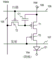
A plurality of pixel circuits are formed on the substrate 100 to control a current to be supplied to the anode of the sub-pixel. Fig. 3B shows a configuration example of the pixel circuit. Each pixel circuit includes a first transistor T1, a second transistor T2, a third transistor T3, and a storage capacitor C1. The pixel circuit controls light emission of the OLED element E1 of the sub-pixel. The transistor is a Thin Film Transistor (TFT). Hereinafter, the first to third transistors T1 to T3 are simply referred to as transistors T1 to T3.
The transistor T2 is a switch for selecting a subpixel. The transistor T2 is a p-channel TFT, and its gate terminal is connected to the scanning line 106. The drain terminal is connected to the data line 105. The source terminal is connected to the gate terminal of the transistor T1.
The transistor T1 is a transistor (driving TFT) for driving the OLED element E1. The transistor T1 is a p-channel TFT, and a gate terminal thereof is connected to a source terminal of the transistor T2. The source terminal of the transistor T1 is connected to a power supply line (Vdd) 108. The drain terminal is connected to the source terminal of the transistor T3. The storage capacitor C1 is provided between the gate terminal and the source terminal of the transistor T1.
The transistor T3 is a switch for controlling the supply/stop of the driving current to the OLED element E1. The transistor T3 is a p-channel TFT, and its gate terminal is connected to the emission control line 107. The source terminal of the transistor T3 is connected to the drain terminal of the transistor T1. The drain terminal is connected to the OLED element E1.
Next, an operation of the pixel circuit is described. The scan driver 131 outputs a selection pulse to the scan line 106 to turn on the transistor T2. The data voltage supplied from the driver IC 134 through the data line 105 is stored to the storage capacitor C1. The storage capacitor C1 holds the stored voltage during a period of one frame. The conductance of the transistor T1 is changed in an analog manner according to the stored voltage, so that the transistor T1 supplies a forward bias current corresponding to the light emission level to the OLED element E1.
The transistor T3 is located on the supply path of the driving current. The emission driver 132 outputs a control signal to the emission control line 107 to control the transistor T3 to be turned on or off. When the transistor T3 is turned on, a driving current is supplied to the OLED element E1. When the transistor T3 is turned off, the supply is stopped. The lighting period (duty ratio) in the period of one field can be controlled by turning on and off the transistor T3.
Fig. 3C shows another configuration example of the pixel circuit. The difference from the pixel circuit in fig. 3B is a transistor T2a and a transistor T3. The transistor T2a is a switch having the same function as the transistor T2 in fig. 3B, or a switch for selecting a subpixel.
Transistor T3 may be used for various purposes. For example, the transistor T3 may be used to reset the anode of the OLED element E1 to a sufficiently low voltage below the black signal level at a time to prevent crosstalk caused by leakage current between the OLED elements E1. For convenience, a reset line for controlling the gate of the transistor T3 is denoted by reference numeral 107, which is the same as the reference numeral of the emission control line 107 in fig. 3B.
Transistor T3 may also be used to measure the characteristics of transistor T1. For example, by measuring the current flowing from the power supply line (Vdd) 108 to the reference voltage supply line (Vref) 109 under bias conditions selected such that the transistor T1 will operate in the saturation region and the switching transistor T3 will operate in the linear region, the voltage-current characteristics of the transistor T1 can be accurately measured. If the difference in voltage-current characteristics between the transistors T1 of the respective sub-pixels is compensated by generating a data signal at an external circuit, a highly uniform display image can be obtained.
Meanwhile, when the transistor T1 is turned off and the transistor T3 operates in the linear region, by applying the voltage for lighting the OLED element E1 from the reference voltage supply line 109, the voltage-current characteristic of the OLED element E1 can be accurately measured. In the case where the OLED element E1 is deteriorated due to long-term use, for example, if the deterioration is compensated for by generating a data signal at an external circuit, the display device may have a long lifetime.
The circuit configurations in fig. 3B and 3C are examples; the pixel circuits may have different circuit configurations. Although the pixel circuits in fig. 3B and 3C employ p-channel TFTs, the pixel circuits may employ n-channel TFTs.
Pixel configuration in Delta-Nabla panel
Fig. 4 shows the pixel arrangement in a delta-nabla panel. Fig. 4 schematically shows a partial region including the boundary (edge) of the display region 125. Fig. 4 shows a portion having a convex curved boundary. Curve 255 represents the virtual design boundary of display area 125. The arrangement of pixels and sub-pixels on the edge of the display area 125 is determined from the curve 255. Hereinafter, the portion including the convex or concave curved boundary is referred to as an R angle.
The display area 125 is composed of a plurality of red sub-pixels 41R, a plurality of green sub-pixels 41G, and a plurality of blue sub-pixels 41B disposed in a plane. In fig. 4, as an example, one of the red sub-pixels, one of the green sub-pixels, and one of the blue sub-pixels are provided with reference numerals. The same hatched rounded rectangles in fig. 4 represent subpixels of the same color. Although the sub-pixels in fig. 4 have a rectangular shape, the sub-pixels may have a desired shape, such as a hexagon or an octagon.
The display area 125 includes a plurality of sub-pixel columns 42 arranged side by side in the X direction. In fig. 4, as an example, one of the sub-pixel columns is provided with reference numeral 42. Each sub-pixel column 42 is composed of sub-pixels arranged one above the other in the Y direction in fig. 4. The X direction (first direction) is a direction extending from the left side to the right side of fig. 4, and the Y direction (second direction) is a direction extending from the top to the bottom of fig. 4. The X-direction and the Y-direction are perpendicular to each other in a plane in which the sub-pixels are arranged.
Each of the sub-pixel columns 42 is composed of red, green, and blue sub-pixels 41R, 41G, and 41B, which are sequentially arranged at a predetermined pitch. In the example of fig. 4, the sub-pixels are cyclically arranged in the order of the red sub-pixel 41R, the blue sub-pixel 41B, and the green sub-pixel 41G. Two sub-pixel columns 42 adjacent to each other are positioned differently in the Y direction; each subpixel of one subpixel column 42 is located between subpixels of two other colors in another subpixel column 42 in the Y direction.
In the example of fig. 4, each sub-pixel column is shifted by half a pitch relative to an adjacent sub-pixel column. One pitch is the distance between subpixels of the same color in the Y direction. For example, the green sub-pixel is located midway between the red sub-pixel and the blue sub-pixel of the adjacent sub-pixel column 42 in the Y direction.
The display area 125 includes a plurality of sub-pixel rows 43 disposed one on another in the Y direction. In fig. 4, as an example, one of the green sub-pixel rows is provided with reference numeral 43. Each sub-pixel row 43 is composed of sub-pixels arranged side by side in the X direction at a predetermined pitch. In the example of fig. 4, each sub-pixel row 43 is composed of sub-pixels of the same color. Each sub-pixel row 43 is sandwiched by sub-pixel rows of the other two colors in the Y direction.
In the X direction, each subpixel of the subpixel rows 43 is located between subpixels adjacent to each other in an adjacent subpixel row 43. In the example of fig. 4, each subpixel row is shifted by half a pitch relative to an adjacent subpixel row. One pitch is the distance between the sub-pixels adjacent to each other in the sub-pixel row 43. The sub-pixels are located at the middle between two sub-pixels adjacent to each other in the adjacent sub-pixel row 43 in the X direction.
In the present embodiment, for descriptive purposes, the sub-pixel lines extending in the X direction are referred to as sub-pixel rows, and the sub-pixel lines extending in the Y direction are referred to as sub-pixel columns; however, the orientations of the sub-pixel rows and sub-pixel columns are not limited to these examples.
The display area 125 includes two types of pixels arranged in a matrix. The two types of pixels are a first type of pixel 51 and a second type of pixel 52. In fig. 4, as an example, only one first type pixel is provided with reference numeral 51 and only one second type pixel is provided with reference numeral 52. The first type of pixel or the second type of pixel is a delta pixel in a delta-nabla arrangement and the remainder are nabla pixels.
In fig. 4, some of the first type pixels 51 are indicated by triangles oriented such that one of the vertices is on the left and the other two vertices are on the right. In addition, some of the second type pixels 52 are indicated by triangles that are oriented such that one of the vertices is to the right and the other two vertices are to the left. The right side in fig. 4 is on the X-direction side, and the left side in fig. 4 is on the opposite side in the X-direction. The pixels 51 may be referred to as second type pixels and the pixels 52 may be referred to as first type pixels.
The first type pixel 51 and the second type pixel 52 are each composed of one green sub-pixel 41G and red sub-pixels 41R and blue sub-pixels 41B adjacent (closest) to the green sub-pixel 41G in the sub-pixel column 42 adjacent to the sub-pixel 41G.
In the first type pixel 51, the red sub-pixel 41R and the blue sub-pixel 41B are sequentially arranged in the same sub-pixel column 42. The sub-pixel column 42 including the green sub-pixel 41G is adjacent to the sub-pixel column 42 including the red sub-pixel 41R and the blue sub-pixel 41B on the X-direction side or on the right side in fig. 4. The green sub-pixel 41G is located between the red sub-pixel 41R and the blue sub-pixel 41B, more specifically, in the middle between the red sub-pixel 41R and the blue sub-pixel 41B in the Y direction.
In the second type pixel 52, the red sub-pixel 41R and the blue sub-pixel 41B are sequentially arranged in the same sub-pixel column 42. The sub-pixel column 42 including the green sub-pixel 41G is adjacent to the sub-pixel column 42 including the red sub-pixel 41R and the blue sub-pixel 41B on the opposite side in the X direction or on the left side in fig. 4. The green sub-pixel 41G is located between the red sub-pixel 41R and the blue sub-pixel 41B, more specifically, in the middle between the red sub-pixel 41R and the blue sub-pixel 41B in the Y direction.
The display area 125 includes a plurality of pixel rows (pixel lines extending in the X direction) extending in the X direction and disposed one on another in the Y direction. The plurality of pixel rows includes two types of pixel rows: a first type pixel row 61 and a second type pixel row 62. In fig. 4, as an example, one of the first type pixel rows is provided with reference numeral 61. Further, as an example, one of the second type pixel rows is provided with reference numeral 62.
The first-type pixel row 61 is composed of first-type pixels 51 arranged side by side in the X direction. The second-type pixel row 62 is composed of the second-type pixels 52 arranged side by side in the X direction. In the display area 125, the first-type pixel rows 61 and the second-type pixel rows 62 are alternately arranged in the Y direction.
The display area 125 includes a plurality of pixel columns (pixel lines extending in the Y direction) 63 extending in the Y direction and arranged side by side in the X direction. In fig. 4, as an example, one of the pixel columns is provided with reference numeral 63. Each pixel column is composed of first-type pixels 51 and second-type pixels 52 alternately arranged in the Y direction at a predetermined pitch.
Fig. 5 illustrates an end pixel included in a portion of the display region 125 illustrated in fig. 4. The end pixels are pixels disposed at the end of the pixel row and the end of the pixel column. The end pixels of the first type of pixels are referred to as first type end pixels and the end pixels of the second type of pixels are referred to as second type end pixels. The pixels disposed at least at the end of the pixel row or at the end of the pixel column are referred to as boundary pixels. The end pixels are also boundary pixels. The location of the boundary pixels is determined from the boundary 255.
Fig. 5 includes first-type end pixels 51A to 51E and second- type end pixels 52A, 52B, and 52C. For example, the first-type end pixel 51D is located at the left end of the first-type pixel row 61A and also at the upper end of the pixel column 63B. The second-type end pixels 52A are located at the left end of the second-type pixel row 62A and also at the upper end of the pixel columns 63A. The pixel row or pixel column may be composed of a single pixel. The individual pixels are arranged at the ends of pixel rows or pixel columns.
Since the end pixels are located at the ends of the pixel rows and the ends of the pixel columns, the end pixels are exposed to the outside of the display area in both directions along the pixel rows and the pixel columns. In the example of fig. 5, the first-type end pixels 51A to 51E and the second- type end pixels 52A, 52B, and 52C are disposed at the left end (end on the opposite side in the X direction) of the pixel row and at the upper end (end on the opposite side in the Y direction) of the pixel column. The first-type end pixels 51A to 51E and the second- type end pixels 52A, 52B, and 52C are exposed at the left side (on the opposite side in the X direction) and the top side (on the opposite side in the Y direction).
The first-type end pixels 51A to 51E are exposed at the green sub-pixel 41G therein. The second type end pixels 52A, 52B, and 52C are exposed at opposite positions of the green sub-pixel 41G therein (at the red sub-pixel 41R and the blue sub-pixel 41B therein). In other words, the green sub-pixels 41G of the first type end pixels 51A to 51E are oriented toward the outside of the display area 125, and the green sub-pixels 41G of the second type end pixels 52A, 52B, and 52C are oriented toward the inside of the display area 125.
As shown in fig. 5, in each of the first type end pixels 51A to 51E, the angle between the vector directed from the centroid of the pixel toward its green subpixel 41G and the normal vector directed outward at the point on the display area boundary 255 closest to the centroid is an acute angle. In contrast, in each of the second type end pixels 52A, 52B, and 52C, the angle between the vector pointing from the centroid of the pixel toward its green subpixel 41G and the normal vector pointing outward at the point on the display area boundary 255 closest to the centroid is an obtuse angle.
Brightness adjustment
The inventors' study revealed that if the green sub-pixel is oriented outward, it is apparent that the end pixel at R (its green sub-pixel) highlights the jaggies at R. For this reason, the OLED display device 10 relatively reduces the brightness of the pixels at the R angle that are clearly seen.
That is, the OLED display device 10 reduces the luminance of a specific end pixel to a level lower than that of other pixels in response to the same input signal. This operation (smoothing) makes the saw-tooth at the R angle less noticeable.
Specifically, the OLED display device 10 reduces the luminance of the first-type end pixels 51A to 51E to a level relatively lower than that of the inner pixel 56. The internal pixels 56 are pixels surrounded by other pixels, more specifically, pixels adjacent to other pixels in four directions of the X direction, the opposite direction of the X direction, the Y direction, and the opposite direction of the Y direction.
The OLED display device 10 reduces the luminance of the first type end pixels 51A to 51E to a level lower than the luminance of the inner pixel 56 in response to the same input picture signal. The OLED display device 10 may reduce the luminance of a portion of the first type end pixels 51A to 51E (e.g., only the first type end pixels 51A and 52B) to a level lower than the luminance of the inner pixel 56.
The end pixels comprising the outwardly directed green sub-pixels are more visible than the end pixels comprising the inwardly directed green sub-pixels and the border pixels other than the end pixels. The OLED display device 10 reduces the luminance of the first type end pixels 51A to 51E to a level lower than the luminance of the second type end pixels 52A, 52B, and 52C in response to the same input picture signal. In addition, the OLED display device 10 reduces the luminance of the first type end pixels 51A to 51E to a level lower than the luminance of the boundary pixels that are not the end pixels in response to the same input picture signal.
The OLED display device 10 equalizes the luminance of the end pixels including the inwardly directed green sub-pixels with the luminance of the inner pixels and the boundary pixels other than the end pixels in response to the same input picture signal. This is because there is no significant difference in visibility between the end pixels comprising the inwardly directed green sub-pixels and the interior pixels or boundary pixels that are not end pixels. The luminance of the end pixels, including the inwardly directed green sub-pixels, may be lower than the luminance of the interior pixels and/or boundary pixels that are not end pixels.
Fig. 5 shows a convex R-angle. The OLED display device 10 may assign different luminance values to end pixels including outwardly directed green sub-pixels included in the convex R-angle. Fig. 6 shows an example of assigning different luminance values to end pixels comprising outwardly directed green sub-pixels at the convex R-angle.
As shown in fig. 6, the R angle includes a plurality of end pixels differently positioned in the X direction and the Y direction. In the example of fig. 6, the positions of the first-type end pixels 51A to 51E and the second- type end pixels 52A, 52B, and 52C are different in the X-direction and the Y-direction. Further, in the convex R angle, the green sub-pixels 41G of the first type end pixels 51B, 51C, and 51D between the green sub-pixels 41G of the first type end pixels 51A and 51E are located further outside than the line 256 connecting the green sub-pixels 41G of the first type end pixels 51A and 51E.
In the example shown in fig. 6, the OLED display device 10 reduces the luminance of the first type end pixels 51B to a level lower than the luminance of the first type end pixels 51C, 51D, and 51E in response to the same input picture signal. This is because the first type end pixels 51B can be seen more clearly than the first type end pixels 51C, 51D and 51E.
The first-type end pixels 51B are adjacent to the second-type pixels 53A in the lower side or Y direction. The second-type pixels 53A are boundary pixels located at the end of the second-type pixel row, and are exposed (do not have adjacent second-type pixels) on the left side or on the opposite side in the X direction.
In contrast, the first-type end pixel 51C is adjacent to the second-type pixel 53B, for example, in the Y direction (on the lower side). On the left side of the second type pixel 53B there is another second type end pixel 52A. In other words, the second-type pixels 53B are adjacent to the second-type end pixels 52A disposed on the opposite sides in the X direction. The other first- type end pixels 51D and 51E each have another second-type pixel disposed at the lower left.
For example, the relative luminance converter 342 multiplies each of the luminance values Y in the first-type end pixels 51A to 51E by a predetermined correction coefficient to reduce their luminance to a level lower than that of the other pixels. Pixel Y R,G,B The brightness value of alpha is k ×(d/255) γ To calculate, wherein alpha k Represents a correction coefficient, d represents a scale value, and γ represents a gamma value.
In the example, let the correction coefficient of the first type end pixels 51A, 51C and 51D be α 2 The correction coefficient of the first-type end pixel 51B is α 3 And the correction coefficient of the first-type end pixel 51E is α 1 Then satisfy alpha 0 (=1.0)>α 1 >α 2 >α 3 Is a relationship of (3). The correction coefficient of other boundary pixels in FIG. 6 is α 0 (=1.0). Therefore, in the pixel shown in fig. 6, the luminance of the first-type end pixel 51B is lowest for the same input signal.
As understood from the foregoing formulas, chromaticity is maintained in the luminance adjustment of the pixels. Therefore, a color change caused by brightness adjustment can be prevented. Such operation of relatively reducing the luminance of the pixel that is more clearly seen in the end pixels including the outwardly directed green sub-pixels can more effectively prevent deterioration of image quality.
Luminance correction coefficient alpha for end pixels including outwardly directed green sub-pixels k Determined according to the setting of the pixel. In an example, the luminance correction coefficient α k Determined from the radius of curvature of the boundary 255 at the end pixel including the outwardly directed green sub-pixel. For example, in an end pixel comprising an outwardly directed green sub-pixel, a point on the boundary 255 closest to the centroid of the end pixel is selected and the radius of curvature of the boundary 255 at that point is determined. When the radius of curvature is large, a smaller luminance correction coefficient α is allocated k . For example, a plurality of curvature radius ranges are defined, and each range is assigned a luminance correction coefficient α k 。
In another example, the luminance correction coefficient α of an end pixel including an outwardly-directed green sub-pixel is determined based on an angle with an adjacent end pixel having the outwardly-directed green sub-pixel k . Fig. 7 shows an example of the angle of an end pixel comprising an outwardly directed green sub-pixel with an adjacent end pixel comprising an outwardly directed green sub-pixel. The first-type end pixel 511A is sandwiched by the first- type end pixels 511B and 511C adjacent thereto.
An inside angle or an angle of opening toward the display area between a line connecting a specific point of the first type end pixel 511A and a corresponding point of the first type end pixel 511B and a line connecting the same point of the first type end pixel 511A and a corresponding point of the first type end pixel 511C is represented by θ1. Determining a luminance correction coefficient α to be assigned to the first-type end pixel 511A based on the angle θ1 k . When the angle θ1 is smaller, a smaller luminance correction coefficient α is allocated k . For example, a plurality of ranges are defined for the angle θ1, and each range is assigned a luminance correction coefficient α k 。
Next, an example of the concave R angle is described. Fig. 8 shows another example of pixel arrangement in a delta-nabla panel. Fig. 8 schematically shows a partial region including the boundary (edge) of the display region 125. Fig. 8 shows a portion having a concavely curved border 255.
In fig. 8, as an example, only one of the first-type pixels is provided with reference numeral 51, and only one of the second-type pixels is provided with reference numeral 52. In fig. 8, as an example, one of the first-type pixel rows is provided with reference numeral 61, and one of the second-type pixel rows is provided with reference numeral 62. Further, in fig. 8, as an example, one of the pixel columns is provided with reference numeral 63. The description provided with reference to fig. 4 applies to the first type of pixels, the second type of pixels, the first type of pixel rows, the second type of pixel rows and the pixel columns.
Fig. 9 shows first-type end pixels 51A to 51D and second-type end pixels 52A to 52D at concave R angles. For example, the first-type end pixels 51C are located at the left end of the first-type pixel row 61A and the upper end of the pixel column 63B. The second-type end pixels 52D are located at the left end of the second-type pixel row 62A and at the upper end of the pixel column 63A.
Since the end pixels are located at the ends of the pixel rows and the ends of the pixel columns, the end pixels are exposed to the outside of the display area in both directions along the pixel rows and the pixel columns. In the example of fig. 9, the first-type end pixels 51A to 51D and the second-type end pixels 52A to 52D are disposed at the left end (end on the opposite side in the X direction) of the pixel row and the upper end (end on the opposite side in the Y direction) of the pixel column. The first-type end pixels 51A to 51D and the second-type end pixels 52A to 52D are exposed at the left side (on the opposite side in the X direction) and the top side (on the opposite side in the Y direction).
The first-type end pixels 51A to 51D are exposed at the green sub-pixel 41G therein. The second type end pixels 52A to 52D are exposed at the opposite of the green sub-pixel 41G therein (at the red sub-pixel 41R and the blue sub-pixel 41B therein). In other words, the green sub-pixels 41G of the first type end pixels 51A to 51D are oriented toward the outside of the display area 125, and the green sub-pixels 41G of the second type end pixels 52A to 52D are oriented toward the inside of the display area 125.
As shown in fig. 9, in each of the first type end pixels 51A to 51D, the angle between the vector directed from the centroid of the pixel toward its green subpixel 41G and the normal vector directed outward at the point on the display area boundary 255 closest to the centroid is an acute angle. In contrast, in each of the second type end pixels 52A to 52D, the angle between the vector directed from the centroid of the pixel toward its green subpixel 41G and the outwardly directed normal vector at the point on the display area boundary 255 closest to the centroid is an obtuse angle.
The OLED display device 10 reduces the luminance of the first type end pixels 51A to 51D to a level lower than the luminance of the inner pixel 56 in response to the same input picture signal. The OLED display device 10 may reduce the luminance of a portion of the first type end pixels 51A to 51D. For example, the OLED display device 10 reduces the luminance of the first-type end pixels 51A to 51D to a level lower than the luminance of the second-type end pixels 52A to 52D in response to the same input picture signal. In addition, the OLED display device 10 reduces the luminance of the first type end pixels 51A to 51D to a level lower than the luminance of the boundary pixels that are not the end pixels in response to the same input signal.
The OLED display device 10 equalizes the luminance of the second type end pixels 52A to 52D with the luminance of the inner pixel 56 and the boundary pixels that are not end pixels. The second type end pixels 52A-52D may have a lower brightness than the interior pixels 56 and/or boundary pixels that are not end pixels.
Fig. 9 shows a concave R-angle. Fig. 10 shows the positional relationship of end pixels including outwardly directed green sub-pixels at a concave R-angle. In the concave R angle, the green sub-pixels 41G of the first type end pixels 51B and 51C between the green sub-pixels 41G of the first type end pixels 51A and 51D are located further inward than the line 256 connecting the green sub-pixels 41G of the first type end pixels 51A and 51D.
The OLED display device 10 may assign different luminance values to end pixels including outwardly directed green sub-pixels included in the concave R-angle. For example, OLED display device 10 may determine a luminance correction factor (luminance value after adjustment/luminance value before adjustment) of an end pixel including an outwardly-directed green sub-pixel according to a radius of curvature of boundary 255 or an angle with an adjacent end pixel including an outwardly-directed green sub-pixel.
The luminance correction coefficients of the end pixels comprising the outwardly directed green sub-pixels may be different between the concave R-angle and the convex R-angle. Specifically, the luminance of the end pixels including the outwardly directed green sub-pixels in the convex R-angle is adjusted to be lower than the luminance of the end pixels including the outwardly directed green sub-pixels in the concave R-angle. This is because the end pixels comprising the outwardly directed green sub-pixels in the convex R-angle are more clearly seen.
For example, in the display region 125, the luminance correction coefficient of the end pixels including the outwardly directed green sub-pixels in the convex R-angle may be equal to or lower than the luminance correction coefficient of the end pixels including the outwardly directed green sub-pixels in the concave R-angle having the same radius of curvature. For example, the display region 125 may include an end pixel including an outwardly directed green sub-pixel in a convex R-angle with a lower luminance correction coefficient than an end pixel including an outwardly directed green sub-pixel in a concave R-angle having the same radius of curvature.
For example, for the same input picture signal, the minimum luminance value of the end pixels comprising the outwardly oriented green sub-pixels in the convex R-angle may be smaller than the minimum luminance value of the end pixels comprising the outwardly oriented green sub-pixels in the concave R-angle in the display area 125. That is, the minimum luminance correction rate of the end pixels including the outwardly directed green sub-pixels in the convex R-angle is lower than the minimum luminance correction rate of the end pixels including the outwardly directed green sub-pixels in the concave R-angle.
Alternatively, for the same input picture signal, the average value of the luminance values to be assigned to the end pixels including the outwardly directed green sub-pixels in all the convex R-angles may be smaller than the average value of the luminance values to be assigned to the end pixels including the outwardly directed green sub-pixels in all the concave R-angles. The average value of the luminance correction coefficients of the end pixels including the outwardly-directed green sub-pixels in the convex R-angle may be smaller than the average value of the luminance correction coefficients of the end pixels including the outwardly-directed green sub-pixels in the concave R-angle.
As described above, in the concave R angle, deterioration of display quality can be prevented by relatively reducing the luminance of the end pixel including the outwardly-directed green sub-pixel. The brightness adjustment in the present disclosure is applicable to any type of display device other than an OLED display device having a display area of delta-nabla arrangement. Although the OLED display device controls brightness using a driving current of a light emitting element of a subpixel, the liquid crystal display device controls brightness (light to be transmitted) using a voltage applied to liquid crystal.
As described above, embodiments of the present disclosure have been described; however, this disclosure is not limited to the foregoing embodiments. Those skilled in the art may readily modify, add or convert each of the elements of the foregoing embodiments within the scope of the disclosure herein. A portion of the configuration of one embodiment may be replaced with the configuration of another embodiment, or the configuration of an embodiment may be incorporated into the configuration of another embodiment.
Claims (8)
1. A display device, comprising:
a plurality of first type pixel lines each composed of a plurality of first type pixels disposed in a first direction in the display area; and
a plurality of second-type pixel lines each composed of a plurality of second-type pixels arranged in the first direction in the display area,
wherein the plurality of first-type pixel lines and the plurality of second-type pixel lines are alternately arranged in a second direction perpendicular to the first direction,
wherein each first type pixel is composed of a first red sub-pixel and a first blue sub-pixel arranged in the second direction, and a first green sub-pixel arranged along opposite sides of the first red sub-pixel and the first blue sub-pixel in opposite directions of the first direction and between the first red sub-pixel and the first blue sub-pixel in the second direction,
Wherein each second type pixel is composed of a second red sub-pixel and a second blue sub-pixel arranged in the second direction, and a second green sub-pixel arranged along opposite sides of the second red sub-pixel and the second blue sub-pixel in the first direction and between the second red sub-pixel and the second blue sub-pixel in the second direction,
wherein the plurality of first-type pixel lines include a plurality of first-type end pixels, each of the first-type end pixels being disposed at an end on an opposite side of the first direction and at an end on an opposite side of a second direction of the pixel lines extending in the second direction,
wherein the plurality of second-type pixel lines include a plurality of second-type end pixels each disposed at an end on an opposite side of the first direction and at an end on an opposite side of a second direction of the pixel lines extending in the second direction, and
wherein the luminance values of the plurality of first-type end pixels are smaller than the luminance values of the inner pixels surrounded by other pixels in four directions of the first direction, the opposite direction of the first direction, the second direction, and the opposite direction of the second direction in response to the same input picture signal,
Wherein, in response to the same input picture signal, the luminance values of the plurality of second type end pixels are larger than the luminance values of the plurality of first type end pixels.
2. The display device of claim 1, wherein the chromaticity values of the plurality of first type end pixels are equal to the chromaticity values of the inner pixels in response to the same input picture signal.
3. The display device according to claim 1,
wherein the plurality of first type end pixels comprises a first type end pixel and a second first type end pixel,
wherein a second type pixel adjacent to the first type end pixel in the second direction is disposed at an end of a second type pixel line on an opposite side of the first direction,
wherein a second type pixel adjacent to the second first type end pixel in the second direction is adjacent to another second type pixel disposed on an opposite side of the first direction, and
wherein the luminance value of the first type end pixel is smaller than the luminance value of the second first type end pixel in response to the same input picture signal.
4. The display device of claim 1, wherein the luminance values of the plurality of second type end pixels are equal to the luminance values of the inner pixels in response to the same input picture signal.
5. The display device according to claim 1, wherein the green sub-pixel of the first type end pixel sandwiched by the first type end pixels at both ends among the plurality of first type end pixels is located further outside than a straight line connecting the green sub-pixels of the first type end pixels at both ends.
6. The display device according to claim 5,
wherein the plurality of first type end pixels comprises a first type end pixel and a second first type end pixel,
wherein an angle between a straight line connecting the first-type end pixels and the first-type end pixels on both sides of the first-type end pixels is smaller than an angle between a straight line connecting the second first-type end pixels and the first-type end pixels on both sides of the second first-type end pixels, and
wherein the luminance value of the first type end pixel is smaller than the luminance value of the second first type end pixel in response to the same input picture signal.
7. The display device according to claim 1,
wherein the display area comprises a first group of a plurality of first type end pixels and a second group of a plurality of first type end pixels different from the plurality of first type end pixels of the first group,
wherein in the first group, the green sub-pixels of the first type end pixels sandwiched by the first type end pixels at both ends are located further outside than the straight lines connecting the green sub-pixels of the first type end pixels at both ends,
wherein, in the second group, the green sub-pixels of the first type end pixels sandwiched by the first type end pixels at the two ends are located further inward than the straight lines connecting the green sub-pixels of the first type end pixels at the two ends, and
wherein the minimum luminance value in the first group is smaller than the minimum luminance value in the second group in response to the same input picture signal.
8. The display device of claim 1, further comprising:
a pixel circuit configured to control brightness of the plurality of first-type pixels and the plurality of second-type pixels; and
A control device configured to control an operation of the pixel circuit,
wherein the control device is configured to control the pixel circuit such that the luminance values of the plurality of first-type end pixels become smaller than the luminance value of the inner pixel in response to the same input picture signal.
Applications Claiming Priority (2)
| Application Number | Priority Date | Filing Date | Title |
|---|---|---|---|
| JP2018-075536 | 2018-04-10 | ||
| JP2018075536A JP7120792B2 (en) | 2018-04-10 | 2018-04-10 | Display device |
Publications (2)
| Publication Number | Publication Date |
|---|---|
| CN110364106A CN110364106A (en) | 2019-10-22 |
| CN110364106B true CN110364106B (en) | 2023-06-30 |
Family
ID=68096109
Family Applications (1)
| Application Number | Title | Priority Date | Filing Date |
|---|---|---|---|
| CN201910262269.XA Active CN110364106B (en) | 2018-04-10 | 2019-04-02 | Display apparatus |
Country Status (3)
| Country | Link |
|---|---|
| US (1) | US10672857B2 (en) |
| JP (1) | JP7120792B2 (en) |
| CN (1) | CN110364106B (en) |
Families Citing this family (6)
| Publication number | Priority date | Publication date | Assignee | Title |
|---|---|---|---|---|
| CN110034148A (en) * | 2018-01-12 | 2019-07-19 | 超微晶科技(深圳)有限公司 | Display panel and display panel production method |
| CN108519706B (en) * | 2018-03-29 | 2021-05-07 | 武汉华星光电技术有限公司 | Display panel |
| WO2020065858A1 (en) * | 2018-09-27 | 2020-04-02 | シャープ株式会社 | Display device |
| CN110148592B (en) * | 2019-05-21 | 2020-12-11 | 上海天马有机发光显示技术有限公司 | Display panel and display device comprising same |
| KR102673832B1 (en) * | 2020-02-07 | 2024-06-11 | 삼성전자주식회사 | Electronic device including display |
| US11250770B1 (en) * | 2020-09-18 | 2022-02-15 | Himax Technologies Limited | De-jaggy processing system and method for OLED display with curved space |
Citations (3)
| Publication number | Priority date | Publication date | Assignee | Title |
|---|---|---|---|---|
| TW201035938A (en) * | 2009-03-17 | 2010-10-01 | Chi Mei Optoelectronics Corp | Circular display panel and circular display using the same |
| CN105304015A (en) * | 2014-07-24 | 2016-02-03 | 乐金显示有限公司 | Organic light emitting diode display device |
| CN107170364A (en) * | 2017-07-04 | 2017-09-15 | 厦门天马微电子有限公司 | A kind of special-shaped display panel and display device |
Family Cites Families (15)
| Publication number | Priority date | Publication date | Assignee | Title |
|---|---|---|---|---|
| JPS60218626A (en) * | 1984-04-13 | 1985-11-01 | Sharp Corp | Color llquid crystal display device |
| JP4210829B2 (en) * | 2002-03-15 | 2009-01-21 | 株式会社日立プラズマパテントライセンシング | Color image display device |
| JP2009092981A (en) * | 2007-10-10 | 2009-04-30 | Epson Imaging Devices Corp | Display panel |
| JP5025025B2 (en) * | 2009-05-15 | 2012-09-12 | 株式会社ジャパンディスプレイセントラル | Liquid crystal display device and driving method of liquid crystal display device |
| US9417479B2 (en) * | 2011-05-13 | 2016-08-16 | Samsung Display Co., Ltd. | Method for reducing simultaneous contrast error |
| US9058783B2 (en) * | 2011-08-31 | 2015-06-16 | Sharp Kabushiki Kaisha | Liquid-crystal display device |
| KR102357931B1 (en) * | 2015-02-02 | 2022-02-04 | 삼성디스플레이 주식회사 | Angular display substrate and display apparatus having the angular display substrate |
| US10643577B2 (en) * | 2015-12-22 | 2020-05-05 | Sharp Kabushiki Kaisha | Display device |
| JP2017142368A (en) * | 2016-02-10 | 2017-08-17 | パナソニックIpマネジメント株式会社 | Display device, and display method |
| WO2018020332A1 (en) * | 2016-07-29 | 2018-02-01 | Semiconductor Energy Laboratory Co., Ltd. | Display device and method for manufacturing the same |
| KR102523988B1 (en) * | 2016-08-29 | 2023-04-20 | 삼성전자주식회사 | A driving method for a display including a curved display area and a display driving circuit and an electronic device supporting the same |
| KR102530765B1 (en) * | 2016-09-09 | 2023-05-11 | 삼성디스플레이주식회사 | Display device, driving device, and method for driving the display device |
| CN107422516B (en) * | 2017-09-19 | 2020-01-21 | 厦门天马微电子有限公司 | Special-shaped display panel and display device |
| CN107516473B (en) * | 2017-09-19 | 2019-09-24 | 厦门天马微电子有限公司 | Special-shaped display panel and display device |
| CN107622735B (en) * | 2017-09-19 | 2019-12-03 | 厦门天马微电子有限公司 | Special-shaped display panel and display device |
-
2018
- 2018-04-10 JP JP2018075536A patent/JP7120792B2/en active Active
-
2019
- 2019-04-02 CN CN201910262269.XA patent/CN110364106B/en active Active
- 2019-04-10 US US16/380,134 patent/US10672857B2/en active Active
Patent Citations (3)
| Publication number | Priority date | Publication date | Assignee | Title |
|---|---|---|---|---|
| TW201035938A (en) * | 2009-03-17 | 2010-10-01 | Chi Mei Optoelectronics Corp | Circular display panel and circular display using the same |
| CN105304015A (en) * | 2014-07-24 | 2016-02-03 | 乐金显示有限公司 | Organic light emitting diode display device |
| CN107170364A (en) * | 2017-07-04 | 2017-09-15 | 厦门天马微电子有限公司 | A kind of special-shaped display panel and display device |
Also Published As
| Publication number | Publication date |
|---|---|
| CN110364106A (en) | 2019-10-22 |
| JP7120792B2 (en) | 2022-08-17 |
| US10672857B2 (en) | 2020-06-02 |
| US20190312099A1 (en) | 2019-10-10 |
| JP2019184825A (en) | 2019-10-24 |
Similar Documents
| Publication | Publication Date | Title |
|---|---|---|
| CN110364106B (en) | Display apparatus | |
| CN110364552B (en) | Display device and method of manufacturing the same | |
| US11462156B2 (en) | Display device and method of driving display device | |
| CN105789253B (en) | Pixel array, electro-optical device, electric apparatus, and method of driving pixel array | |
| US9680133B2 (en) | Display device | |
| CN110556075B (en) | Display device and method of controlling the same | |
| JP6274771B2 (en) | Light emitting element display device | |
| US11636812B2 (en) | Degradation compensator, display device having the same, and method for compensating image data of the display device | |
| JP6516236B2 (en) | Electro-optical device | |
| CN112309329B (en) | Display device | |
| JP2022021644A (en) | Display | |
| US10672319B2 (en) | Display device and method of converting relative luminance data for picture frame into relative luminance data for display panel | |
| CN110556074B (en) | Display device and method of controlling the same | |
| US11765955B2 (en) | Display device with first delta subpixel arrangement and second delta subpixel arrangement disposed along first and second axes and configured to determine luminance values to be assigned to subpixels and method of controlling the same | |
| US20150070377A1 (en) | Image signal processing circuit, image signal processing method and display apparatus |
Legal Events
| Date | Code | Title | Description |
|---|---|---|---|
| PB01 | Publication | ||
| PB01 | Publication | ||
| TA01 | Transfer of patent application right |
Effective date of registration: 20200907 Address after: Kawasaki City, Kanagawa Prefecture, Japan Applicant after: Tianma Japan, Ltd. Applicant after: WUHAN TIANMA MICROELECTRONICS Co.,Ltd. Address before: Kawasaki City, Kanagawa Prefecture, Japan Applicant before: TIANMA JAPAN, Ltd. |
|
| TA01 | Transfer of patent application right | ||
| SE01 | Entry into force of request for substantive examination | ||
| SE01 | Entry into force of request for substantive examination | ||
| GR01 | Patent grant | ||
| GR01 | Patent grant |