JP7120792B2 - Display device - Google Patents
Display device Download PDFInfo
- Publication number
- JP7120792B2 JP7120792B2 JP2018075536A JP2018075536A JP7120792B2 JP 7120792 B2 JP7120792 B2 JP 7120792B2 JP 2018075536 A JP2018075536 A JP 2018075536A JP 2018075536 A JP2018075536 A JP 2018075536A JP 7120792 B2 JP7120792 B2 JP 7120792B2
- Authority
- JP
- Japan
- Prior art keywords
- pixel
- pixels
- type
- terminal type
- sub
- Prior art date
- Legal status (The legal status is an assumption and is not a legal conclusion. Google has not performed a legal analysis and makes no representation as to the accuracy of the status listed.)
- Active
Links
- 239000000758 substrate Substances 0.000 description 32
- 238000012937 correction Methods 0.000 description 28
- 239000010410 layer Substances 0.000 description 24
- 239000010408 film Substances 0.000 description 10
- 238000007789 sealing Methods 0.000 description 10
- 238000006243 chemical reaction Methods 0.000 description 9
- 238000005538 encapsulation Methods 0.000 description 6
- 230000006866 deterioration Effects 0.000 description 5
- 239000003990 capacitor Substances 0.000 description 4
- 238000000034 method Methods 0.000 description 4
- 239000011521 glass Substances 0.000 description 3
- 239000011229 interlayer Substances 0.000 description 3
- 125000006850 spacer group Chemical group 0.000 description 3
- 239000010409 thin film Substances 0.000 description 3
- 230000001154 acute effect Effects 0.000 description 2
- 238000013461 design Methods 0.000 description 2
- 230000005484 gravity Effects 0.000 description 2
- 239000004973 liquid crystal related substance Substances 0.000 description 2
- 238000012545 processing Methods 0.000 description 2
- 238000009877 rendering Methods 0.000 description 2
- 239000000956 alloy Substances 0.000 description 1
- 229910045601 alloy Inorganic materials 0.000 description 1
- 230000015572 biosynthetic process Effects 0.000 description 1
- 239000003086 colorant Substances 0.000 description 1
- 238000009499 grossing Methods 0.000 description 1
- 230000007774 longterm Effects 0.000 description 1
- 239000011159 matrix material Substances 0.000 description 1
- 239000003870 refractory metal Substances 0.000 description 1
- 239000011347 resin Substances 0.000 description 1
- 229920005989 resin Polymers 0.000 description 1
- 238000012546 transfer Methods 0.000 description 1
Images


Classifications
-
- H—ELECTRICITY
- H10—SEMICONDUCTOR DEVICES; ELECTRIC SOLID-STATE DEVICES NOT OTHERWISE PROVIDED FOR
- H10K—ORGANIC ELECTRIC SOLID-STATE DEVICES
- H10K59/00—Integrated devices, or assemblies of multiple devices, comprising at least one organic light-emitting element covered by group H10K50/00
- H10K59/10—OLED displays
- H10K59/12—Active-matrix OLED [AMOLED] displays
- H10K59/131—Interconnections, e.g. wiring lines or terminals
-
- G—PHYSICS
- G09—EDUCATION; CRYPTOGRAPHY; DISPLAY; ADVERTISING; SEALS
- G09G—ARRANGEMENTS OR CIRCUITS FOR CONTROL OF INDICATING DEVICES USING STATIC MEANS TO PRESENT VARIABLE INFORMATION
- G09G3/00—Control arrangements or circuits, of interest only in connection with visual indicators other than cathode-ray tubes
- G09G3/20—Control arrangements or circuits, of interest only in connection with visual indicators other than cathode-ray tubes for presentation of an assembly of a number of characters, e.g. a page, by composing the assembly by combination of individual elements arranged in a matrix no fixed position being assigned to or needed to be assigned to the individual characters or partial characters
- G09G3/2003—Display of colours
-
- G—PHYSICS
- G09—EDUCATION; CRYPTOGRAPHY; DISPLAY; ADVERTISING; SEALS
- G09G—ARRANGEMENTS OR CIRCUITS FOR CONTROL OF INDICATING DEVICES USING STATIC MEANS TO PRESENT VARIABLE INFORMATION
- G09G3/00—Control arrangements or circuits, of interest only in connection with visual indicators other than cathode-ray tubes
- G09G3/20—Control arrangements or circuits, of interest only in connection with visual indicators other than cathode-ray tubes for presentation of an assembly of a number of characters, e.g. a page, by composing the assembly by combination of individual elements arranged in a matrix no fixed position being assigned to or needed to be assigned to the individual characters or partial characters
- G09G3/2007—Display of intermediate tones
- G09G3/2074—Display of intermediate tones using sub-pixels
-
- G—PHYSICS
- G09—EDUCATION; CRYPTOGRAPHY; DISPLAY; ADVERTISING; SEALS
- G09G—ARRANGEMENTS OR CIRCUITS FOR CONTROL OF INDICATING DEVICES USING STATIC MEANS TO PRESENT VARIABLE INFORMATION
- G09G3/00—Control arrangements or circuits, of interest only in connection with visual indicators other than cathode-ray tubes
- G09G3/20—Control arrangements or circuits, of interest only in connection with visual indicators other than cathode-ray tubes for presentation of an assembly of a number of characters, e.g. a page, by composing the assembly by combination of individual elements arranged in a matrix no fixed position being assigned to or needed to be assigned to the individual characters or partial characters
- G09G3/22—Control arrangements or circuits, of interest only in connection with visual indicators other than cathode-ray tubes for presentation of an assembly of a number of characters, e.g. a page, by composing the assembly by combination of individual elements arranged in a matrix no fixed position being assigned to or needed to be assigned to the individual characters or partial characters using controlled light sources
- G09G3/30—Control arrangements or circuits, of interest only in connection with visual indicators other than cathode-ray tubes for presentation of an assembly of a number of characters, e.g. a page, by composing the assembly by combination of individual elements arranged in a matrix no fixed position being assigned to or needed to be assigned to the individual characters or partial characters using controlled light sources using electroluminescent panels
- G09G3/32—Control arrangements or circuits, of interest only in connection with visual indicators other than cathode-ray tubes for presentation of an assembly of a number of characters, e.g. a page, by composing the assembly by combination of individual elements arranged in a matrix no fixed position being assigned to or needed to be assigned to the individual characters or partial characters using controlled light sources using electroluminescent panels semiconductive, e.g. using light-emitting diodes [LED]
- G09G3/3208—Control arrangements or circuits, of interest only in connection with visual indicators other than cathode-ray tubes for presentation of an assembly of a number of characters, e.g. a page, by composing the assembly by combination of individual elements arranged in a matrix no fixed position being assigned to or needed to be assigned to the individual characters or partial characters using controlled light sources using electroluminescent panels semiconductive, e.g. using light-emitting diodes [LED] organic, e.g. using organic light-emitting diodes [OLED]
- G09G3/3225—Control arrangements or circuits, of interest only in connection with visual indicators other than cathode-ray tubes for presentation of an assembly of a number of characters, e.g. a page, by composing the assembly by combination of individual elements arranged in a matrix no fixed position being assigned to or needed to be assigned to the individual characters or partial characters using controlled light sources using electroluminescent panels semiconductive, e.g. using light-emitting diodes [LED] organic, e.g. using organic light-emitting diodes [OLED] using an active matrix
- G09G3/3233—Control arrangements or circuits, of interest only in connection with visual indicators other than cathode-ray tubes for presentation of an assembly of a number of characters, e.g. a page, by composing the assembly by combination of individual elements arranged in a matrix no fixed position being assigned to or needed to be assigned to the individual characters or partial characters using controlled light sources using electroluminescent panels semiconductive, e.g. using light-emitting diodes [LED] organic, e.g. using organic light-emitting diodes [OLED] using an active matrix with pixel circuitry controlling the current through the light-emitting element
-
- G—PHYSICS
- G09—EDUCATION; CRYPTOGRAPHY; DISPLAY; ADVERTISING; SEALS
- G09G—ARRANGEMENTS OR CIRCUITS FOR CONTROL OF INDICATING DEVICES USING STATIC MEANS TO PRESENT VARIABLE INFORMATION
- G09G3/00—Control arrangements or circuits, of interest only in connection with visual indicators other than cathode-ray tubes
- G09G3/20—Control arrangements or circuits, of interest only in connection with visual indicators other than cathode-ray tubes for presentation of an assembly of a number of characters, e.g. a page, by composing the assembly by combination of individual elements arranged in a matrix no fixed position being assigned to or needed to be assigned to the individual characters or partial characters
- G09G3/22—Control arrangements or circuits, of interest only in connection with visual indicators other than cathode-ray tubes for presentation of an assembly of a number of characters, e.g. a page, by composing the assembly by combination of individual elements arranged in a matrix no fixed position being assigned to or needed to be assigned to the individual characters or partial characters using controlled light sources
- G09G3/30—Control arrangements or circuits, of interest only in connection with visual indicators other than cathode-ray tubes for presentation of an assembly of a number of characters, e.g. a page, by composing the assembly by combination of individual elements arranged in a matrix no fixed position being assigned to or needed to be assigned to the individual characters or partial characters using controlled light sources using electroluminescent panels
- G09G3/32—Control arrangements or circuits, of interest only in connection with visual indicators other than cathode-ray tubes for presentation of an assembly of a number of characters, e.g. a page, by composing the assembly by combination of individual elements arranged in a matrix no fixed position being assigned to or needed to be assigned to the individual characters or partial characters using controlled light sources using electroluminescent panels semiconductive, e.g. using light-emitting diodes [LED]
- G09G3/3208—Control arrangements or circuits, of interest only in connection with visual indicators other than cathode-ray tubes for presentation of an assembly of a number of characters, e.g. a page, by composing the assembly by combination of individual elements arranged in a matrix no fixed position being assigned to or needed to be assigned to the individual characters or partial characters using controlled light sources using electroluminescent panels semiconductive, e.g. using light-emitting diodes [LED] organic, e.g. using organic light-emitting diodes [OLED]
- G09G3/3266—Details of drivers for scan electrodes
-
- G—PHYSICS
- G09—EDUCATION; CRYPTOGRAPHY; DISPLAY; ADVERTISING; SEALS
- G09G—ARRANGEMENTS OR CIRCUITS FOR CONTROL OF INDICATING DEVICES USING STATIC MEANS TO PRESENT VARIABLE INFORMATION
- G09G3/00—Control arrangements or circuits, of interest only in connection with visual indicators other than cathode-ray tubes
- G09G3/20—Control arrangements or circuits, of interest only in connection with visual indicators other than cathode-ray tubes for presentation of an assembly of a number of characters, e.g. a page, by composing the assembly by combination of individual elements arranged in a matrix no fixed position being assigned to or needed to be assigned to the individual characters or partial characters
- G09G3/22—Control arrangements or circuits, of interest only in connection with visual indicators other than cathode-ray tubes for presentation of an assembly of a number of characters, e.g. a page, by composing the assembly by combination of individual elements arranged in a matrix no fixed position being assigned to or needed to be assigned to the individual characters or partial characters using controlled light sources
- G09G3/30—Control arrangements or circuits, of interest only in connection with visual indicators other than cathode-ray tubes for presentation of an assembly of a number of characters, e.g. a page, by composing the assembly by combination of individual elements arranged in a matrix no fixed position being assigned to or needed to be assigned to the individual characters or partial characters using controlled light sources using electroluminescent panels
- G09G3/32—Control arrangements or circuits, of interest only in connection with visual indicators other than cathode-ray tubes for presentation of an assembly of a number of characters, e.g. a page, by composing the assembly by combination of individual elements arranged in a matrix no fixed position being assigned to or needed to be assigned to the individual characters or partial characters using controlled light sources using electroluminescent panels semiconductive, e.g. using light-emitting diodes [LED]
- G09G3/3208—Control arrangements or circuits, of interest only in connection with visual indicators other than cathode-ray tubes for presentation of an assembly of a number of characters, e.g. a page, by composing the assembly by combination of individual elements arranged in a matrix no fixed position being assigned to or needed to be assigned to the individual characters or partial characters using controlled light sources using electroluminescent panels semiconductive, e.g. using light-emitting diodes [LED] organic, e.g. using organic light-emitting diodes [OLED]
- G09G3/3275—Details of drivers for data electrodes
- G09G3/3291—Details of drivers for data electrodes in which the data driver supplies a variable data voltage for setting the current through, or the voltage across, the light-emitting elements
-
- H—ELECTRICITY
- H10—SEMICONDUCTOR DEVICES; ELECTRIC SOLID-STATE DEVICES NOT OTHERWISE PROVIDED FOR
- H10K—ORGANIC ELECTRIC SOLID-STATE DEVICES
- H10K59/00—Integrated devices, or assemblies of multiple devices, comprising at least one organic light-emitting element covered by group H10K50/00
- H10K59/10—OLED displays
- H10K59/12—Active-matrix OLED [AMOLED] displays
- H10K59/121—Active-matrix OLED [AMOLED] displays characterised by the geometry or disposition of pixel elements
- H10K59/1213—Active-matrix OLED [AMOLED] displays characterised by the geometry or disposition of pixel elements the pixel elements being TFTs
-
- H—ELECTRICITY
- H10—SEMICONDUCTOR DEVICES; ELECTRIC SOLID-STATE DEVICES NOT OTHERWISE PROVIDED FOR
- H10K—ORGANIC ELECTRIC SOLID-STATE DEVICES
- H10K59/00—Integrated devices, or assemblies of multiple devices, comprising at least one organic light-emitting element covered by group H10K50/00
- H10K59/30—Devices specially adapted for multicolour light emission
- H10K59/35—Devices specially adapted for multicolour light emission comprising red-green-blue [RGB] subpixels
- H10K59/353—Devices specially adapted for multicolour light emission comprising red-green-blue [RGB] subpixels characterised by the geometrical arrangement of the RGB subpixels
-
- G—PHYSICS
- G09—EDUCATION; CRYPTOGRAPHY; DISPLAY; ADVERTISING; SEALS
- G09G—ARRANGEMENTS OR CIRCUITS FOR CONTROL OF INDICATING DEVICES USING STATIC MEANS TO PRESENT VARIABLE INFORMATION
- G09G2300/00—Aspects of the constitution of display devices
- G09G2300/04—Structural and physical details of display devices
- G09G2300/0421—Structural details of the set of electrodes
- G09G2300/0426—Layout of electrodes and connections
-
- G—PHYSICS
- G09—EDUCATION; CRYPTOGRAPHY; DISPLAY; ADVERTISING; SEALS
- G09G—ARRANGEMENTS OR CIRCUITS FOR CONTROL OF INDICATING DEVICES USING STATIC MEANS TO PRESENT VARIABLE INFORMATION
- G09G2300/00—Aspects of the constitution of display devices
- G09G2300/04—Structural and physical details of display devices
- G09G2300/0439—Pixel structures
- G09G2300/0452—Details of colour pixel setup, e.g. pixel composed of a red, a blue and two green components
-
- G—PHYSICS
- G09—EDUCATION; CRYPTOGRAPHY; DISPLAY; ADVERTISING; SEALS
- G09G—ARRANGEMENTS OR CIRCUITS FOR CONTROL OF INDICATING DEVICES USING STATIC MEANS TO PRESENT VARIABLE INFORMATION
- G09G2310/00—Command of the display device
- G09G2310/02—Addressing, scanning or driving the display screen or processing steps related thereto
- G09G2310/0232—Special driving of display border areas
-
- G—PHYSICS
- G09—EDUCATION; CRYPTOGRAPHY; DISPLAY; ADVERTISING; SEALS
- G09G—ARRANGEMENTS OR CIRCUITS FOR CONTROL OF INDICATING DEVICES USING STATIC MEANS TO PRESENT VARIABLE INFORMATION
- G09G2320/00—Control of display operating conditions
- G09G2320/02—Improving the quality of display appearance
- G09G2320/0233—Improving the luminance or brightness uniformity across the screen
-
- G—PHYSICS
- G09—EDUCATION; CRYPTOGRAPHY; DISPLAY; ADVERTISING; SEALS
- G09G—ARRANGEMENTS OR CIRCUITS FOR CONTROL OF INDICATING DEVICES USING STATIC MEANS TO PRESENT VARIABLE INFORMATION
- G09G2320/00—Control of display operating conditions
- G09G2320/06—Adjustment of display parameters
- G09G2320/0626—Adjustment of display parameters for control of overall brightness
-
- G—PHYSICS
- G09—EDUCATION; CRYPTOGRAPHY; DISPLAY; ADVERTISING; SEALS
- G09G—ARRANGEMENTS OR CIRCUITS FOR CONTROL OF INDICATING DEVICES USING STATIC MEANS TO PRESENT VARIABLE INFORMATION
- G09G2360/00—Aspects of the architecture of display systems
- G09G2360/16—Calculation or use of calculated indices related to luminance levels in display data
-
- G—PHYSICS
- G09—EDUCATION; CRYPTOGRAPHY; DISPLAY; ADVERTISING; SEALS
- G09G—ARRANGEMENTS OR CIRCUITS FOR CONTROL OF INDICATING DEVICES USING STATIC MEANS TO PRESENT VARIABLE INFORMATION
- G09G3/00—Control arrangements or circuits, of interest only in connection with visual indicators other than cathode-ray tubes
- G09G3/20—Control arrangements or circuits, of interest only in connection with visual indicators other than cathode-ray tubes for presentation of an assembly of a number of characters, e.g. a page, by composing the assembly by combination of individual elements arranged in a matrix no fixed position being assigned to or needed to be assigned to the individual characters or partial characters
- G09G3/34—Control arrangements or circuits, of interest only in connection with visual indicators other than cathode-ray tubes for presentation of an assembly of a number of characters, e.g. a page, by composing the assembly by combination of individual elements arranged in a matrix no fixed position being assigned to or needed to be assigned to the individual characters or partial characters by control of light from an independent source
- G09G3/36—Control arrangements or circuits, of interest only in connection with visual indicators other than cathode-ray tubes for presentation of an assembly of a number of characters, e.g. a page, by composing the assembly by combination of individual elements arranged in a matrix no fixed position being assigned to or needed to be assigned to the individual characters or partial characters by control of light from an independent source using liquid crystals
- G09G3/3607—Control arrangements or circuits, of interest only in connection with visual indicators other than cathode-ray tubes for presentation of an assembly of a number of characters, e.g. a page, by composing the assembly by combination of individual elements arranged in a matrix no fixed position being assigned to or needed to be assigned to the individual characters or partial characters by control of light from an independent source using liquid crystals for displaying colours or for displaying grey scales with a specific pixel layout, e.g. using sub-pixels
Description
本開示は、表示装置に関する。 The present disclosure relates to display devices.
カラー表示装置の表示領域は、一般に、表示パネルの基板上に配列された赤(R)、緑(G)、青(B)の副画素で構成されている。副画素の様々な配置(画素配置)が提案されおり、例えば、RGB Straipe配置や、デルタナブラ配置(単にデルタ配置とも呼ぶ)が知られている(例えば特許文献1)。 The display area of a color display device is generally composed of red (R), green (G), and blue (B) sub-pixels arranged on the substrate of the display panel. Various arrangements (pixel arrangements) of sub-pixels have been proposed, and for example, an RGB stripe arrangement and a delta nabla arrangement (also simply called a delta arrangement) are known (for example, Patent Document 1).
近年、表示領域のコーナを曲線状に形成することで、表示領域のデザイン性を向上する製品が増加している。しかし、デルタナブラ配置では、曲線状のコーナ部(Rコーナ部とも呼ぶ)の刻み目が目立ちやすく、画質が低下する。 2. Description of the Related Art In recent years, there has been an increase in the number of products in which the design of the display area is improved by forming the corners of the display area in a curved shape. However, in the delta nabla arrangement, notches in curved corners (also called R corners) are easily conspicuous, and image quality deteriorates.
したがって、デルタナブラ配置の表示装置において、Rコーナ部における画質低下を抑制できる技術が望まれる。 Therefore, in a display device with a delta nabla arrangement, there is a demand for a technique capable of suppressing deterioration in image quality at the R corner portion.
本開示の一態様の表示装置は、表示領域において、それぞれ第1方向に配列された複数の第1種画素からなる、複数の第1種画素ラインと、前記表示領域において、それぞれ前記第1方向に配列された複数の第2種画素からなる、複数の第2種画素ラインと、を含む。前記複数の第1種画素ラインと前記複数の第2種画素ラインとは、前記第1方向に垂直な第2方向に交互に配列されている。前記第1種画素は、前記第2方向に配列された第1赤副画素及び第1青副画素、並びに、前記第1赤副画素及び前記第1青副画素に対して前記第1方向と反対の側に配置され、かつ、前記第2方向において前記第1赤副画素及び前記第1青副画素の間に配置されている第1緑副画素、から構成されている。前記第2種画素は、前記第2方向に配列された第2赤副画素及び第2青副画素、並びに、前記第2赤副画素及び前記第2青副画素に対して前記第1方向の側に配置され、かつ、前記第2方向において前記第2赤副画素及び前記第2青副画素の間に配置されている第2緑副画素、から構成されている。前記複数の第1種画素ラインは、前記第1の方向の反対側の端に配置されており、かつ、前記第2方向に配列されている画素ラインにおける前記第2方向の反対側の端に配置されている、複数の終端第1種画素を含む。前記複数の第2種画素ラインは、前記第1の方向の反対側の端に配置されており、かつ、前記第2方向に配列されている画素ラインにおける前記第2方向の反対側の端に配置されている、複数の終端第2種画素を含む。前記複数の終端第1種画素それぞれの輝度は、同一の入力映像信号に対して、前記第1方向、前記第1方向の反対方向、前記第2方向、及び前記第2方向の反対方向の4方向において他の画素に囲まれている内部画素の輝度よりも小さい。
A display device according to one aspect of the present disclosure includes, in a display region, a plurality of first-type pixel lines each composed of a plurality of first-type pixels arranged in a first direction; a plurality of type 2 pixel lines, each of which is composed of a plurality of type 2 pixels arranged in rows. The plurality of first-type pixel lines and the plurality of second-type pixel lines are alternately arranged in a second direction perpendicular to the first direction. The first-type pixels include first red sub-pixels and first blue sub-pixels arranged in the second direction, and the first red sub-pixels and the first blue sub-pixels arranged in the first direction. a first green subpixel disposed on opposite sides and disposed between the first red subpixel and the first blue subpixel in the second direction. The second-type pixels include second red sub-pixels and second blue sub-pixels arranged in the second direction, and a second green sub-pixel arranged on the side of the pixel and arranged between the second red sub-pixel and the second blue sub-pixel in the second direction. The plurality of
本開示の一態様によれば、デルタナブラ配置の表示装置において画質低下を抑制することができる。 According to one aspect of the present disclosure, deterioration in image quality can be suppressed in a display device with a delta nabla arrangement.
以下、添付図面を参照して本開示の実施形態を説明する。本実施形態は本発明を実現するための一例に過ぎず、本開示の技術的範囲を限定するものではないことに注意すべきである。各図において共通の構成については同一の参照符号が付されている。 Embodiments of the present disclosure will be described below with reference to the accompanying drawings. It should be noted that this embodiment is merely an example for realizing the present invention and does not limit the technical scope of the present disclosure. The same reference numerals are given to the common components in each figure.
[表示装置の構成]
図1を参照して、本実施形態に係る、表示装置の全体構成を説明する。なお、説明をわかりやすくするため、図示した物の寸法、形状については、誇張して記載している場合もある。以下において、表示装置の例として、OLED(Organic Light-Emitting Diode)表示装置を説明するが、本開示の特徴は、液晶表示装置や量子ドット表示装置等、OLED表示装置と異なる任意の種類の表示装置に適用することができる。
[Configuration of display device]
The overall configuration of the display device according to the present embodiment will be described with reference to FIG. In order to make the description easier to understand, the dimensions and shapes of the illustrated objects may be exaggerated. In the following, an OLED (Organic Light-Emitting Diode) display device will be described as an example of a display device. It can be applied to the device.
図1は、OLED表示装置10の構成例を模式的に示す。OLED表示装置10は、OLED表示パネルと制御装置とを含む。OLED表示パネルは、発光素子が形成されるTFT(Thin Film Transistor)基板100と、OLED素子を封止する封止基板200と、TFT基板100と封止基板200とを接合する接合部(ガラスフリットシール部)300を含む。TFT基板100と封止基板200との間には、例えば、乾燥空気が封入されており、接合部300により封止されている。
FIG. 1 schematically shows a configuration example of an
TFT基板100の表示領域125の外側のカソード電極形成領域114の周囲に、走査ドライバ131、エミッションドライバ132、保護回路133、及びドライバIC134が配置されている。これらは、FPC(Flexible Printed Circuit)135を介して外部の機器と接続される。ドライバIC134は制御装置に含まれる。走査ドライバ131、エミッションドライバ132、及び保護回路133は、制御装置、又は、OLED表示パネル及び制御装置に含まれる。
A
走査ドライバ131はTFT基板100の走査線を駆動する。エミッションドライバ132は、エミッション制御線を駆動して、各副画素の発光期間を制御する。保護回路133は素子を静電気放電から保護する。ドライバIC134は、例えば、異方性導電フィルム(ACF:Anisotropic Conductive Film)を用いて実装される。
A
ドライバIC134は、走査ドライバ131及びエミッションドライバ132に電源及びタイミング信号(制御信号)を与え、さらに、データ線に映像データに対応する信号を与える。すなわち、ドライバIC134は、表示制御機能を有する。後述するように、ドライバIC134は、映像フレームの画素の相対輝度データを表示パネルの副画素の相対輝度データに変換する機能を有する。
The driver IC 134 supplies a power source and timing signals (control signals) to the
図1において、左から右に延びる軸をX軸、上から下に延びる軸をY軸と呼ぶ。走査線はX軸に沿って延びており、表示領域125において、X軸に沿って配列された画素又は副画素を画素又は副画素の行と呼ぶ。表示領域125において、Y軸に沿って配列された画素又は副画素を画素列又は副画素の列と呼ぶ。
In FIG. 1, the axis extending from left to right is called the X-axis, and the axis extending from top to bottom is called the Y-axis. The scan lines run along the X-axis, and the pixels or sub-pixels arranged along the X-axis in the
次に、OLED表示装置10の詳細構造について説明する。図2は、OLED表示装置10の断面構造の一部を模式的に示す。図2に示すように、OLED表示装置10は、TFT基板100と、TFT基板100と対向する封止構造部とを含む。ここで、封止構造部の一例は、可撓性又は不撓性の封止基板200である。封止構造部は、例えば、薄膜封止(TFE:Thin Film Encapsulation)構造であってもよい。
Next, the detailed structure of the
TFT基板100は、絶縁基板151と封止構造部との間に配置された、複数の下部電極(例えば、アノード電極162)と、1つの上部電極(例えば、カソード電極166)と、複数の有機発光層165とを含む。カソード電極166は、有機発光層165(有機発光膜165とも記す)からの光を封止構造部に向けて透過させる透明電極である。
The
1つのカソード電極166と1つのアノード電極162との間に、1つの有機発光層165が配置されている。複数のアノード電極162は、同一面上(例えば、平坦化膜161の上)に配置され、1つのアノード電極162の上に1つの有機発光層165が配置されている。
One organic light-emitting
OLED表示装置10は、封止構造部に向かって立ち上がる複数のスペーサ164と、それぞれが複数のスイッチを含む複数の回路とを有する。複数の回路の各々は、絶縁基板151とアノード電極162との間に形成され、複数のアノード電極162の各々に供給する電流を制御する。
OLED
図2は、トップエミッション型の画素構造の例を示す。トップエミッション型の画素構造は、光が出射する側(図面上側)に、複数の画素に共通のカソード電極166が配置される。カソード電極166は、表示領域125の全面を完全に覆う形状を有する。本開示の特徴は、ボトムエミッション型の画素構造を有するOLED表示装置にも適用できる。ボトムエミッション型の画素構造は、透明アノード電極と反射カソード電極を有し、TFT基板100を介して外部に光を出射する。
FIG. 2 shows an example of a top-emission pixel structure. In the top emission type pixel structure, a
以下、OLED表示装置10についてより詳しく説明する。TFT基板100は、表示領域125内に配列された副画素、及び、表示領域125の周囲の配線領域に形成された配線を含む。配線は、画素回路と、配線領域に配置された回路131、132、134とを接続する。
The
本実施形態の表示領域125は、デルタナブラ配置された副画素で構成されている。デルタナブラ配置の詳細は後述する。以下において、OLED表示パネルを、デルタナブラパネルと呼ぶことがある。副画素は、赤(R)、緑(G)、又は青(B)のいずれかの色を表示する発光領域である。以下に説明する例は、上記三色の組により画像を表示するが、OLED表示装置10は、これと異なる三色の組により表示してもよい。
The
発光領域は、OLED素子に含まれる。OLED素子は、下部電極であるアノード電極、有機発光層、及び上部電極であるカソード電極を含んで構成される。すなわち、複数のOLED素子は、1つのカソード電極166と、複数のアノード電極162と、複数の有機発光層165により形成されている。
A light emitting region is included in the OLED device. An OLED device includes an anode electrode as a lower electrode, an organic light-emitting layer, and a cathode electrode as an upper electrode. That is, multiple OLED elements are formed by one
絶縁基板151は、例えばガラス又は樹脂で形成されており、不撓性又は可撓性基板である。なお、以下の説明において、絶縁基板151に近い側を下側、遠い側を上側と記す。ゲート絶縁膜156を介して、ゲート電極157が形成されている。ゲート電極157の層上に層間絶縁膜158が形成されている。
The insulating
表示領域125内において、層間絶縁膜158上にソース電極159、ドレイン電極160が形成されている。ソース電極159、ドレイン電極160は、例えば、高融点金属又はその合金で形成される。ソース電極159、ドレイン電極160は、層間絶縁膜158のコンタクトホールに形成されたコンタクト部168、169によって、チャネル部155に接続されている。
A
ソース電極159、ドレイン電極160の上に、絶縁性の平坦化膜161が形成される。絶縁性の平坦化膜161の上に、アノード電極162が形成されている。アノード電極162は、平坦化膜161のコンタクトホールに形成されたコンタクト部によってドレイン電極160に接続されている。画素回路(TFTs)は、アノード電極162の下側に形成されている。
An insulating
アノード電極162の上に、OLED素子を分離する絶縁性の画素定義層(Pixel Defining Layer:PDL)163が形成されている。OLED素子は、積層された、アノード電極162、有機発光層165、及びカソード電極166(の部分)で構成される。発光領域OLED素子は、画素定義層163の開口167に形成されている。
An insulating pixel defining layer (PDL) 163 separating the OLED elements is formed on the
絶縁性のスペーサ164は、2つのアノード電極162の間における、画素定義層163の面上に形成されている。スペーサ164の頂面は画素定義層163の上面よりも高い(封止基板200に近い)位置にあり、封止基板200が変形した場合に、封止基板200を支持して、OLED素子と封止基板200との間隔を維持する。
An insulating
アノード電極162の上に、有機発光層165が形成されている。有機発光層165は、画素定義層163の開口167及びその周囲において、画素定義層163に付着している。有機発光層165の上にカソード電極166が形成されている。カソード電極166は、透明電極である。カソード電極166は、有機発光層165からの可視光の全て又は一部を透過させる。
An organic
画素定義層163の開口167に形成された、アノード電極162、有機発光層165及びカソード電極166の積層膜が、OLED素子を構成する。電流は画素定義層163の開口167のみに流れので、開口167において露出している有機発光層165の領域が、OLED素子の発光領域(副画素)である。カソード電極166は、分離して形成されているアノード電極162及び有機発光層165(OLED素子)に共通である。なお、カソード電極166の上には、不図示のキャップ層が形成されてもよい。
A stack of
封止基板200は、透明な絶縁基板であって、例えばガラス基板である。封止基板200の光出射面(前面)に、λ/4位相差板201と偏光板202とが配置され、外部から入射した光の反射を抑制する。
The sealing
[ドライバICの構成]
図3Aは、ドライバIC134の論理要素を示す。ドライバIC134は、ガンマ変換部341、相対輝度変換部342、逆ガンマ変換部343、駆動信号生成部344、及びデータドライバ345を含む。
[Configuration of Driver IC]
FIG. 3A shows the logic elements of
ドライバIC134は、不図示の主制御部から、映像信号及び映像信号用タイミング信号を受信する。映像信号は、連続する映像フレームのデータ(信号)を含む。ガンマ変換部341は、入力された映像信号に含まれるRGB階調値(信号)を、RGB相対輝度値に変換する。より具体的には、ガンマ変換部341は、各映像フレームの各画素のR階調値、G階調値、B階調値を、R相対輝度値、G相対輝度値、B相対輝度値(LRin、LGin、LBin)に変換する。画素の相対輝度値は、映像フレーム内で正規化された輝度値である。
The
相対輝度変換部342は、映像フレーム内の各画素のR、G、B相対輝度値(LRin、LGin、LBin)を、OLED表示パネルの副画素のR、G、B相対輝度値(LRp、LGp、LBp)に変換する。副画素の相対輝度値は、OLED表示パネルにおいて正規化された副画素の輝度値である。
The
なお、表示すべき画像データの画素数と表示パネルの画素数は必ずしも一致するとは限らず、レンダリング処理によって見かけ上の解像度を向上させることもできる。その場合には、レンダリング処理後に最終的に表示パネルの副画素に割り当てられた各画素のR、G、B相対輝度値(LRin、LGin、LBin)に対して、上記処理を行いOLED表示パネルの副画素のR、G、B相対輝度値(LRp、LGp、LBp)に変換する。 Note that the number of pixels of image data to be displayed does not necessarily match the number of pixels of the display panel, and the apparent resolution can be improved by rendering processing. In that case, the R, G, and B relative luminance values (LRin, LGin, and LBin) of each pixel finally assigned to the sub-pixels of the display panel after the rendering process are subjected to the above process, and the Convert to R, G, B relative luminance values (LRp, LGp, LBp) of sub-pixels.
後述するように、相対輝度変換部342は、特定のパネル画素を構成する副画素の相対輝度値を調整する。具体的には、相対輝度変換部342は、同一の入力信号に対して、特定画素の相対輝度値を他の画素の相対輝度値よりも小さくなるように決定する。なお、相対輝度変換部342と異なる機能部、例えば、ガンマ変換部341が、特定画素の輝度を調整する処理を行ってもよい。
As will be described later, the
逆ガンマ変換部343は、相対輝度変換部342による演算後のR副画素、G副画素、B副画素の相対輝度値を、R副画素、G副画素、B副画素の階調値に変換する。データドライバ345は、R副画素、G副画素、B副画素の階調値に応じた駆動信号を、画素回路に送信する。
The inverse
駆動信号生成部344は、入力された映像信号用タイミング信号を、OLED表示パネルの表示制御用駆動信号に変換する。映像信号用タイミング信号は、データ転送レートを決定するドットクロック(ピクセルクロック)、水平同期信号、垂直同期信号、データイネーブル信号を含む。
The
駆動信号生成部344は、入力された映像信号用タイミング信号のドットクロック、データイネーブル信号、垂直同期信号、水平同期信号から、デルタナブラパネルのデータドライバ345、走査ドライバ131、及びエミッションドライバ132の制御信号(又は、パネルの駆動信号)を生成し、それらに出力する。
The driving
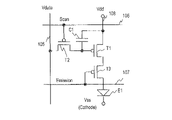
[画素回路]
基板100上には、複数の副画素のアノード電極にそれぞれ供給する電流を制御する複数の画素回路が形成されている。図3Bは、画素回路の構成例を示す。各画素回路は、第1のトランジスタT1と、第2のトランジスタT2と、第3のトランジスタT3と、保持容量C1とを含む。画素回路は、副画素であるOLED素子E1の発光を制御する。トランジスタは、TFT(Thin Film Transistor)である。以下、第1のトランジスタT1~第3のトランジスタT3をそれぞれトランジスタT1~トランジスタT3と略記する。
[Pixel circuit]
A plurality of pixel circuits are formed on the
トランジスタT2は副画素選択用のスイッチである。トランジスタT2はpチャネル型TFTであり、ゲート端子は、走査線106に接続されている。ドレイン端子は、データ線105に接続されている。ソース端子は、トランジスタT1のゲート端子に接続されている。
The transistor T2 is a switch for sub-pixel selection. The transistor T2 is a p-channel TFT, and its gate terminal is connected to the
トランジスタT1はOLED素子E1の駆動用のトランジスタ(駆動TFT)である。トランジスタT1はpチャネル型TFTであり、そのゲート端子はT2のソース端子に接続されている。トランジスタT1のソース端子は電源線108(Vdd)に接続されている。ドレイン端子は、トランジスタT3のソース端子に接続されている。トランジスタT1のゲート端子とソース端子との間に保持容量C1が形成されている。 The transistor T1 is a transistor (driving TFT) for driving the OLED element E1. Transistor T1 is a p-channel TFT whose gate terminal is connected to the source terminal of T2. A source terminal of the transistor T1 is connected to the power supply line 108 (Vdd). The drain terminal is connected to the source terminal of transistor T3. A holding capacitor C1 is formed between the gate terminal and the source terminal of the transistor T1.
トランジスタT3は、OLED素子E1への駆動電流の供給と停止を制御するスイッチである。トランジスタT3はpチャネル型TFTであり、ゲート端子はエミッション制御線107に接続されている。トランジスタT3のソース端子はトランジスタT1のドレイン端子に接続されている。ドレイン端子は、OLED素子E1に接続されている。
The transistor T3 is a switch that controls supply and stop of the driving current to the OLED element E1. The transistor T3 is a p-channel TFT and has a gate terminal connected to the
次に、画素回路の動作を説明する。走査ドライバ131が走査線106に選択パルスを出力し、トランジスタT2を開状態にする。データ線105を介してドライバIC134から供給されたデータ電圧は、保持容量C1に格納される。保持容量C1は、格納された電圧を、1フレーム期間を通じて保持する。保持電圧によって、トランジスタT1のコンダクタンスがアナログ的に変化し、トランジスタT1は、発光諧調に対応した順バイアス電流をOLED素子E1に供給する。
Next, the operation of the pixel circuit will be described. The
トランジスタT3は、駆動電流の供給経路上に位置する。エミッションドライバ132は、エミッション制御線107に制御信号を出力して、トランジスタT3開閉状態を制御する。トランジスタT3が開状態のとき、駆動電流がOLED素子E1に供給される。トランジスタT3が閉状態のとき、この供給が停止される。トランジスタT3の開閉を制御することにより、1フィールド周期内の点灯期間(デューティ比)を制御することができる。
The transistor T3 is located on the drive current supply path. The
図3Cは、画素回路の他の構成例を示す。図3Bの画素回路との相違は、トランジスタT2aと、トランジスタT3である。トランジスタT2aは、図3BのトランジスタT2の機能(副画素選択用のスイッチ)と同じ機能を有するスイッチである。 FIG. 3C shows another configuration example of the pixel circuit. The difference from the pixel circuit of FIG. 3B is the transistor T2a and the transistor T3. The transistor T2a is a switch having the same function as the transistor T2 in FIG. 3B (switch for sub-pixel selection).
トランジスタT3は、様々な目的で使用することができる。トランジスタT3は、例えば、OLED素子E1間のリーク電流によるクロストークを抑制するために、一旦、OLED素子E1のアノード電極を黒信号レベル以下の十分低い電圧にリセットする目的で使用しても良い。 Transistor T3 can be used for various purposes. For example, the transistor T3 may be used for the purpose of temporarily resetting the anode electrode of the OLED element E1 to a sufficiently low voltage below the black signal level in order to suppress crosstalk due to leakage current between the OLED elements E1.
他にも、トランジスタT3は、トランジスタT1の特性を測定する目的で使用してもよい。例えば、トランジスタT1を飽和領域、スイッチングトランジスタT3を線形領域で動作するようにバイアス条件を選んで、電源線108(Vdd)から基準電圧供給線109(Vref)に流れる電流を測定すれば、トランジスタT1の電圧・電流変換特性を正確に測定することができる。副画素毎のトランジスタT1の電圧・電流変換特性の違いを補償するデータ信号を外部回路で生成すれば、均一性の高い表示画像を実現できる。 Alternatively, transistor T3 may be used to measure the characteristics of transistor T1. For example, if the bias conditions are selected so that the transistor T1 operates in the saturation region and the switching transistor T3 operates in the linear region, and the current flowing from the power supply line 108 (Vdd) to the reference voltage supply line 109 (Vref) is measured, the transistor T1 voltage-to-current conversion characteristics can be accurately measured. If an external circuit generates a data signal that compensates for the difference in voltage-current conversion characteristics of the transistor T1 for each sub-pixel, a highly uniform display image can be realized.
一方、トランジスタT1をオフ状態にしてトランジスタT3をリニア領域で動作させ、OLED素子E1を発光させる電圧を基準電圧供給線109から印加すれば、副画素毎のOLED素子E1の電圧・電流特性を正確に測定することができる。例えば、長時間の使用によってOLED素子E1が劣化した場合にも、その劣化量を補償するデータ信号を外部回路で生成すれば、長寿命化を実現できる。
On the other hand, if the transistor T1 is turned off, the transistor T3 is operated in the linear region, and a voltage that causes the OLED element E1 to emit light is applied from the reference
図3B及び3Cの画素回路は例であって、画素回路は他の回路構成を有してよい。図3B及び3Cの画素回路はpチャネル型TFTを使用しているが、画素回路はnチャネル型TFTを使用してもよい。 The pixel circuits of FIGS. 3B and 3C are examples, and the pixel circuits may have other circuit configurations. Although the pixel circuits of FIGS. 3B and 3C use p-channel TFTs, the pixel circuits may also use n-channel TFTs.
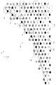
[デルタナブラパネルにおける画素配置]
図4は、デルタナブラパネルにおける画素配置を示す。図4は、表示領域125の境界(表示領域125の端)を含む一部の領域を模式的に示す。図4は、凸状の曲線的な境界を示す部分を示す。曲線255は、表示領域125の設計上の仮想的な境界線を示す。曲線255に従って、表示領域125の端の画素及び副画素の配置が決定されている。以下において、凸状又は凹上の曲線的な境界を示す部分を、Rコーナ部とも呼ぶ。
[Pixel Arrangement in Delta Nabla Panel]
FIG. 4 shows the pixel arrangement in a delta nabla panel. FIG. 4 schematically shows a partial area including the boundary of the display area 125 (the edge of the display area 125). FIG. 4 shows a section showing a convex curvilinear boundary. A
表示領域125は、面内に配置されている、複数の赤副画素41R、複数の緑副画素41G、及び複数の青副画素41Bで構成されている。図4において、一つの赤副画素、一つの緑副画素、及び一つの青副画素が、例として、符号で指示されている。図4において、同一のハッチングの(丸い角の)四角は、同一色の副画素を示す。図4において、副画素の形状は四角であるが、副画素の形状は任意であって、例えば、六角形又は八角形であってもよい。
The
表示領域125は、X方向に配列されている複数の副画素列42を含む。図4において、一つの副画素列が、例として、符号42で指示されている。副画素列42は、図4において、Y方向に配列されている副画素で構成されている。X方向(第1方向)は、図4において左から右に向かう方向であり、Y方向(第2方向)は、上から下に向かう方向である。X方向とY方向は、副画素が配置されている面内において垂直である。
The
副画素列42は、所定ピッチで交互に配列された赤副画素41R、緑副画素41G及び青副画素41Bで構成されている。図4の例において、赤副画素41R、青副画素41B、及び緑副画素41Gは、この順で配列されている。隣接する副画素列42の位置は、Y方向においてずれており、副画素列42の副画素は、Y方向において、隣接する副画素列42の他の二色の副画素の間にある。
The
図4の例において、隣接する副画素列42は半ピッチずれている。1ピッチは、同一色の副画素の間のY方向における距離である。例えば、緑副画素は、Y方向において、隣接副画素列42における赤副画素と青副画素の中央に位置している。
In the example of FIG. 4, adjacent
表示領域125は、Y方向に配列されている複数の副画素行43を含む。図4において、一つの緑の副画素行が、例として、符号43で指示されている。副画素行43は、X方向に所定ピッチで配列されている副画素で構成されている。図4の例において、各副画素行43は、同一色の副画素で構成されている。副画素行43は、他の2色の副画素行にY方向において挟まれている。
The
副画素行43の副画素は、X方向において、隣接する副画素行43の隣接する二つの副画素の間に位置する。図4の例において、隣接する副画素行43は半ピッチずれている。1ピッチは、副画素行43において隣接する副画素の間の距離である。副画素は、X方向において、隣接する副画素行43の隣接する二つの副画素の中央に位置する。
A subpixel in the
なお、本実施形態においては、便宜的に、X方向に延びる副画素ラインを副画素行、Y方向に延びる副画素ラインを副画素列と呼ぶが、副画素行及び副画素列の方向は、これに限定されない。 In this embodiment, for the sake of convenience, a subpixel line extending in the X direction is called a subpixel row, and a subpixel line extending in the Y direction is called a subpixel column. It is not limited to this.
表示領域125は、マトリックス状に配置されている、第1種画素51及び第2種画素52の、2種類の画素を含む。図4において、一つの第1種画素のみが、例として、符号51で指示されている。また、一つの第2種画素のみが、例として、符号52で指示されている。第1種画素及び第2種画素の一方が、デルタナブラ配置におけるデルタ画素であり、もう一方がナブラ画素である。
The
図4において、いくつかの第1種画素51は、一つの頂点が左側にあり、二つの頂点が右側にある三角形で示されている。また、いくつかの第2種画素52は、一つの頂点が右側にあり、二つの頂点が左側にある三角形で示されている。図4における右側がX方向の側であり、左側がその反対側である。なお、画素51が第2種画素と呼び、画素52を第1種画素と呼んでもよい。
In FIG. 4, some
第1種画素51及び第2種画素52は、それぞれ、一つ緑副画素41Gと、当該緑副画素41Gに隣接する副画素列42において、当該緑副画素41Gに隣接する(最も近い)赤副画素41R及び青副画素41Bで構成されている。
The
第1種画素51において、赤副画素41R及び青副画素41Bは、同一の副画素列42において連続して配置されている。緑副画素41Gが含まれる副画素列42は、赤副画素41R及び青副画素41が含まれる副画素列42、X方向の反対側、つまり、図4における左側に隣接している。緑副画素41Gは、Y方向において、赤副画素41Rと青副画素41Bの間、より具体的には中央に位置している。
In the
第2種画素52において、赤副画素41R及び青副画素41Bは、同一の副画素列42において連続して配置されている。緑副画素41Gが含まれる副画素列42は、赤副画素41R及び青副画素41が含まれる副画素列42、X方向の側、つまり、図4における右側に隣接している。緑副画素41Gは、Y方向において、赤副画素41Rと青副画素41Bの間、より具体的には中央に位置している。
In the type 2
表示領域125は、X方向に延び、Y方向に配列されている複数の画素行(X方向延びる画素ライン)を含む。複数の画素行は、第1種画素行61及び第2種画素行62の2種類の画素行で構成されている。図4において、一つの第1種画素行が、例として、符号61で指示されている。また、一つの第2種画素行が、例として、符号62で指示されている。
The
第1種画素行61は、X方向に配列された第1種画素51で構成されている。第2種画素行62は、X方向に配列された第2種画素52で構成されている。表示領域125において、第1種画素行61及び第2種画素行62は、Y方向において交互に配列されている。
The first
表示領域125は、Y方向に延び、X方向に配列されている複数の画素列(Y方向延びる画素ライン)63を含む。図4において、一つの画素列が、例として、符号63で指示されている。各画素列は、Y方向に所定ピッチで交互に配列された、第1種画素51及び第2種画素52で構成されている。
The
図5は、図4に示す表示領域125の部分に含まれる終端画素を示す。終端画素は、画素行及び画素列双方の端に配置されている画素である。第1種画素の終端画素を、終端第1種画素と呼び、第2種画素の終端画素を、終端第2種画素と呼ぶ。また、画素行又は画素列の少なくとも一方の端に配置されている画素を境界画素と呼ぶ。終端画素は境界画素でもある。境界画素の位置は、境界線255に応じて決定されている。
FIG. 5 shows the end pixels included in the portion of the
図5は、終端第1種画素51A~51E、並びに、終端第2種画素52A、52B及び52Cを示す。例えば、第1種画素51Dは、第1種画素行61Aの左端に位置し、さらに、画素列63Bの上端に位置する。第2種画素52Aは、第2種画素行62Aの左端に位置し、さらに、画素列63Aの上端に位置する。なお、画素行又は画素列は、単一の画素で構成されていてもよい。当該単一画素は、その画素行又は画素列の端に配置されている。
FIG. 5 shows
終端画素は画素行及び画素列の端に位置しているため、画素行及び画素列それぞれに沿った2方向において表示領域の外部に露出している。図5の例において、終端第1種画素51A~51E、並びに、終端第2種画素52A、52B及び52Cは、画素行の左端(X方向の反対側の端)及び画素列の上端(Y方向の反対側の端)に配置されている。終端第1種画素51A~51E、並びに、終端第2種画素52A、52B及び52Cは、左側(X方向の反対側)及び上側(Y方向の反対側)において露出している。
Since the terminal pixels are located at the ends of the pixel rows and pixel columns, they are exposed to the outside of the display area in two directions along the pixel rows and pixel columns, respectively. In the example of FIG. 5, the
終端第1種画素51A~51Eは、それらの緑副画素41Gの側において、露出している。一方、終端第2種画素52A、52B、52Cは、それらの緑副画素41Gと反対側(赤副画素41R及び青副画素41Bの側)において、露出している。言い換えれば、終端第1種画素51A~51Eの緑副画素41Gは、表示領域125の外側を向いており、終端第2種画素52A、52B、52Cの緑副画素41Gは、表示領域125の内側を向いている。
The
図5に示すように、終端第1種画素51A~51Eの重心から緑副画素41Gに向かうベクトルと、表示領域境界線255の上記重心に最も近い点の外側に向かう法線ベクトルとの間の角度は、鋭角である。反対に、終端第2種画素52A、52B及び52Cの重心から緑副画素41Gに向かうベクトルと、表示領域境界線255の上記重心に最も近い点の外側に向かう法線ベクトルとの間の角度は、鈍角である。
As shown in FIG. 5, between the vector directed from the centroid of the
[輝度調整]
発明者の検討によれば、Rコーナ部において、終端画素の緑副画素が外向きである場合、その終端画素(の緑副画素)が視認されやすく、Rコーナ部における刻み目が目立ちやすい。そこで、OLED表示装置10は、Rコーナ部において視認されやすい画素の輝度を相対的に低下させる。
[Brightness adjustment]
According to the inventor's study, when the green sub-pixel of the terminal pixel faces outward at the R corner, the terminal pixel (the green sub-pixel of the terminal pixel) is easily visible, and the notch at the R corner is easily noticeable. Therefore, the
つまり、OLED表示装置10は、同一の入力信号に対して、特定の終端画素の輝度を、他の画素の輝度よりも低くする。これにより、Rコーナ部における刻み目を目立ちにくくすることができる(スムージング処理)。
In other words, the
具体的には、OLED表示装置10は、終端第1種画素51A~51Eの輝度を、内部画素56の輝度よりも相対的に低くする。内部画素56は、周囲を他の画素に囲まれている画素であり、より具体的には、X方向、X方向の反対方向、Y方向及びY方向の反対方向の4方向において、他の画素に隣接している画素である。
Specifically, the
OLED表示装置10は、同一の入力映像信号に対して、終端第1種画素51A~51Eの輝度を内部画素56の輝度よりも低くする。なお、終端第1種画素51A~51Eの一部の輝度のみ、例えば、終端第1種画素51A~51Eおいて終端第1種画素51A及び51Bのみを、内部画素56の輝度より低くしてもよい。
The
緑副画素外向き終端画素は、緑副画素内向き終端画素よりも視認されやすく、また、終端画素以外の境界画素よりも視認されやすい。OLED表示装置10は、例えば、同一の入力映像信号に対して、終端第1種画素51A~51Eの輝度を、終端第2種画素52A、52B、52Cの輝度よりも低くする。また、OLED表示装置10は、同一の入力映像信号に対して、終端第1種画素51A~51Eの輝度を、終端画素ではない境界画素の輝度よりも低くする。
The green subpixel outward end pixel is more visible than the green subpixel inward end pixel, and is more visible than the border pixels other than the end pixel. The
OLED表示装置10は、同一の入力映像信号に対して、緑副画素内向き終端画素の輝度を、内部画素及び終端画素ではない境界画素と同一にする。緑副画素内向き終端画素と内部画素及び終端画素ではない境界画素の視認性に大きな違いはないからである。緑副画素内向き終端画素の輝度は、内部画素及び/又は終端画素ではない境界画素の輝度よりも低くてもよい。
For the same input video signal, the
図5は、凸状のRコーナ部を示す。OLED表示装置10は、凸状のRコーナ部に含まれる緑副画素外向き画素において、異なる輝度を与えてもよい。図6は、凸状のRコーナ部における緑副画素外向き画素において、異なる輝度を与える例を示す。
FIG. 5 shows a convex R corner portion. The
図6に示すように、Rコーナ部は、X方向及びY方向における位置が異なる複数の終端画素を含む。図6の例において、終端第1種画素51A~51E及び終端第2種画素52A、52B、52Cの位置は、X方向及びY方向において異なる。さらに、凸状のRコーナ部において、終端第1種画素51A及び51Eの緑副画素41Gを結ぶ線256に対して、それらの間の終端第1種画素51B、51C、及び51Dの緑副画素41Gは、外側に配置されている。
As shown in FIG. 6, the R corner portion includes a plurality of terminal pixels whose positions in the X and Y directions are different. In the example of FIG. 6, the positions of the
図6に示す例において、OLED表示装置10は、同一入力映像信号に対して、終端第1種画素51Bの輝度を、他の終端第1種画素51C、51D、51Eよりも小さくする。終端第1種画素51Bは、終端第1種画素51C、51D、51Eよりも視認されやすいからである。
In the example shown in FIG. 6, the
終端第1種画素51Bは、下側、つまりY方向において、第2種画素53Aに隣接している。第2種画素53Aは、第2種画素行の端に配置されている境界画素であり、左側、つまり、X方向の反対側において、露出している(隣接第2種画素が存在しない)。
The
一方、例えば、終端第1種画素51Cは、Y方向(下側)において、第2種画素53Bに隣接している。第2種画素53Bの左側には、終端第2種画素52Aが存在している。つまり、第2種画素53Bは、X方向の反対側に配置されている終端第2種画素52Aに隣接している。他の終端第1種画素51D、51Eの左斜め下にも、第2種画素が配置されている。
On the other hand, for example, the
例えば、相対輝度変換部342は、終端第1種画素51A~51Eの輝度Yのそれぞれに、所定の補正係数を掛けることで、他の画素よりも相対的に輝度を小さくすることができる。画素の輝度YR、G、Bは、αk×(d/255)γで計算される。ここで、αkは補正係数、dは階調レベル、そしてγはガンマ値である。
For example, the relative
一例において、終端第1種画素51A、51C、51Dの補正係数がα2、終端第1種画素51Bの補正係数がα3、終端第1種画素51Eの補正係数がα1である。α0(=1.0)>α1>α2>α3の関係が成立する。図6における他の境界画素の補正係数はα0(=1.0)である。したがって、図6に示す画素において、終端第1種画素51B輝度が、同一入力信号に対して、最も小さい。
In one example, the correction coefficient for the
上記数式から理解されるように、画素の輝度補正において色度は維持される。したがって、輝度補正により色変化を防止することができる。このように、緑副画素外向き終端画素のうち、より視認されやすい画素の輝度を相対的に低くすることで、画質の低下をより効果的に防ぐことができる。 As can be seen from the above equations, chromaticity is preserved in pixel luminance correction. Therefore, color change can be prevented by luminance correction. In this way, by relatively lowering the brightness of pixels that are more visible among the green sub-pixel outward end pixels, it is possible to more effectively prevent deterioration in image quality.
緑副画素外向き終端画素の輝度補正係数αkは、画素配置に応じて決定されている。一例において、輝度補正係数αkは、緑副画素外向き終端画素における境界線255の曲率半径に応じて決定される。例えば、緑副画素外向き終端画素の重心から最も近い境界線255上の点が選択され、その点における境界線255の曲率半径が決定される。曲率半径が大きい程、小さい輝度補正係数αkが与えられる。例えば、曲率半径の複数の範囲が定義され、範囲それぞれに輝度補正係数αkが割り当てられる。
The brightness correction coefficient α k of the green subpixel outward end pixel is determined according to the pixel arrangement. In one example, the brightness correction factor α k is determined according to the radius of curvature of the
他の例において、緑副画素外向き終端画素の輝度補正係数αkは、隣接する緑副画素外向き終端画素との間の角度に基づいて決定される。図7は、緑副画素外向き終端画素と、隣接する緑副画素外向き終端画素との間の角度の例を示す。終端第1種画素511Aは、隣接する終端第1種画素511B、511Cに挟まれている。
In another example, the intensity correction factor α k of the green subpixel outward-facing end-pixel is determined based on the angle between adjacent green sub-pixel outward-facing end-pixels. FIG. 7 shows an example of the angle between a green subpixel outward facing end pixel and an adjacent green subpixel outward facing end pixel. The
終端第1種画素511Aの所定位置と終端第1種画素511Bの所定位置とを結ぶ直線と、終端第1種画素511Aの所定位置と終端第1種画素511Cの所定位置とを結ぶ直線と、の間の内側角度、つまり表示領域側の角度は、θ1で表わされている。終端第1種画素511Aに割り当てる補正係数αkは、角度θ1に基づいて決定される。角度θ1が小さい程、小さい補正係数αkが割り当てられる。例えば、角度θ1の間の範囲が定義され、範囲それぞれに輝度補正係数αkが割り当てられる。
A straight line connecting a predetermined position of the
次に凹状のRコーナ部の例を説明する。図8は、デルタナブラパネルにおける画素配置の他の例を示す。図8は、表示領域125の境界(表示領域125の端)を含む一部の領域を模式的に示す。図8は、凹状の曲線的な境界255を示す部分を示す。
Next, an example of a concave R corner portion will be described. FIG. 8 shows another example of pixel arrangement in a delta nabla panel. FIG. 8 schematically shows a partial area including the boundary of the display area 125 (end of the display area 125). FIG. 8 shows a portion showing a concave
図8において、一つの第1種画素のみが、例として、符号51で指示されている。また、一つの第2種画素のみが、例として、符号52で指示されている。図8において、一つの第1種画素行が、例として、符号61で指示されている。また、一つの第2種画素行が、例として、符号62で指示されている。図8において、一つの画素列が、例として、符号63で指示されている。第1種画素、第2種画素、第1種画素行、第2種画素行及び画素列に対して、図4を参照した説明が適用される。
In FIG. 8, only one
図9は、凹状Rコーナ部における、終端第1種画素51A~51D、並びに、終端第2種画素52A~52Dを示す。例えば、第1種画素51Cは、第1種画素行61Aの左端に位置し、さらに、画素列63Bの上端に位置する。第2種画素52Dは、第2種画素行62Aの左端に位置し、さらに、画素列63Aの上端に位置する。
FIG. 9 shows
終端画素は画素行及び画素列の端に位置しているため、画素行及び画素列それぞれに沿った2方向において表示領域の外部に露出している。図9の例において、終端第1種画素51A~51D、並びに、終端第2種画素52A~52Dは、画素行の左端(X方向の反対側の端)及び画素列の上端(Y方向の反対側の端)に配置されている。終端第1種画素51A~51D、並びに、終端第2種画素52A~52Dは、左側(X方向の反対側)及び上側(Y方向の反対側)において露出している。
Since the terminal pixels are located at the ends of the pixel rows and pixel columns, they are exposed to the outside of the display area in two directions along the pixel rows and pixel columns, respectively. In the example of FIG. 9, the
終端第1種画素51A~51Dは、それらの緑副画素41Gの側において、露出している。一方、終端第2種画素52A~52Dは、それらの緑副画素41Gと反対側(赤副画素41R及び青副画素41Bの側)において、露出している。言い換えれば、終端第1種画素51A~51Dの緑副画素41Gは、表示領域125の外側を向いており、終端第2種画素52A~52Dの緑副画素41Gは、表示領域125の内側を向いている。
The
図9に示すように、終端第1種画素51A~51Dの重心から緑副画素41Gに向かうベクトルと、表示領域境界線255の上記重心に最も近い点の外側に向かう法線ベクトルとの間の角度は、鋭角である。反対に、終端第2種画素52A~52Dの重心から緑副画素41Gに向かうベクトルと、表示領域境界線255の上記重心に最も近い点の外側に向かう法線ベクトルとの間の角度は、鈍角である。
As shown in FIG. 9, the vector between the centroids of the
OLED表示装置10は、同一の入力映像信号に対して、終端第1種画素51A~51Dの輝度を内部画素56の輝度よりも低くする。なお、終端第1種画素51A~51Dの一部の輝度のみを、内部画素56の輝度より低くしてもよい。OLED表示装置10は、例えば、同一の入力映像信号に対して、終端第1種画素51A~51Dの輝度を、終端第2種画素52A~52Dの輝度よりも低くする。また、OLED表示装置10は、同一の入力映像信号に対して、終端第1種画素51A~51Dの輝度を、終端画素ではない境界画素の輝度よりも低くする。
The
OLED表示装置10は、同一の入力映像信号に対して、終端第2種画素52A~52Dの輝度を、内部画素56及び終端画素ではない境界画素と同一にする。終端第2種画素52A~52Dの輝度は、内部画素56及び/又は終端画素ではない境界画素の輝度よりも低くてもよい。
For the same input video signal, the
図9は、凹状のRコーナ部を示す。図10は、凹状のRコーナ部における緑副画素外向き終端画素の位置関係を示す。凹状のRコーナ部において、終端第1種画素51A及び51Dの緑副画素41Gを結ぶ線256に対して、それらの間の終端第1種画素51B及び51Cの緑副画素41Gは、内側に配置されている。
FIG. 9 shows a concave R corner. FIG. 10 shows the positional relationship of green sub-pixel outward end pixels in the concave R corner portion. In the concave R corner portion, the green sub-pixels 41G of the
OLED表示装置10は、凹状のRコーナ部に含まれる緑副画素外向き画素において、異なる輝度を与えてもよい。例えば、境界線255の曲率半径又は隣接緑副画素外向き終端画素との間の角度に応じて、緑副画素外向き終端画素に与える輝度補正率(補正後輝度/補正前輝度)を決定してもよい。
The
凹状Rコーナ部と凸状Rコーナ部の間で、緑副画素外向き終端画素に与える輝度補正率が異なっていてもよい。具体的には、凸状Rコーナ部の緑副画素外向き終端画素の輝度を、凹状Rコーナ部の緑副画素外向き終端画素の輝度よりも小さくする。凸状Rコーナ部の緑副画素外向き終端画素の方が、視認されやすいからである。 The luminance correction factor applied to the green sub-pixel outward end pixel may be different between the concave R-corner portion and the convex R-corner portion. Specifically, the brightness of the green sub-pixel outward-facing end pixel in the convex R-corner portion is set lower than the brightness of the green sub-pixel outward-facing end pixel in the concave R-corner portion. This is because the green sub-pixel outward-facing terminal pixel in the convex R corner portion is easier to be visually recognized.
例えば、表示領域125において、同一曲率半径における、凸状のRコーナ部内の緑副画素外向き終端画素の輝度補正率が、凹状のRコーナ部内の緑副画素外向き終端画素の輝度補正率以下である。例えば、表示領域125は、輝度補正率が、同一曲率半径における凹状のRコーナ部内の緑副画素外向き終端画素の輝度補正率より小さい、凸状のRコーナ部内の緑副画素外向き終端画素を含んでもよい。
For example, in the
例えば、表示領域125において、同一入力映像信号に対し、凸状Rコーナ部の緑副画素外向き終端画素の最小輝度値を、凹状のRコーナ部に含まれる緑副画素外向き画素の最小輝度値よりも小さい。つまり、凸状Rコーナ部の緑副画素外向き終端画素の輝度補正率の最小値が、凹状のRコーナ部に含まれる緑副画素外向き画素の輝度補正率の最小値よりも小さい。
For example, in the
または、同一入力映像信号に対して、全ての凸状Rコーナ部の緑副画素外向き終端画素の輝度の平均値は、全ての凹状のRコーナ部の緑副画素外向き終端画素の輝度の平均値よりも小さい。凸状Rコーナ部の緑副画素外向き終端画素の輝度補正率の平均値が、凹状のRコーナ部に含まれる緑副画素外向き画素の輝度補正率の平均値よりも小さい。 Alternatively, for the same input video signal, the average value of the brightness of the outward-facing end pixels of the green subpixels of all the convex R-corners is the brightness of the outward-facing end pixels of the green subpixels of all the concave R-corners. Smaller than average. The average value of the brightness correction factors of the green subpixel outward-facing end pixels in the convex R corner portion is smaller than the average value of the brightness correction factors of the green subpixel outward pixels included in the concave R corner portion.
以上のように、凹状のRコーナ部においても、緑副画素外向き終端画素の輝度を相対的に小さくすることで、表示品質の低下を抑制することができる。なお、本開示の輝度補正は、デルタナブラ画素配置の表示領域を含む、OLED表示装置と異なる任意の種類の表示装置に適用することができる。OLED表示装置は、副画素の発光素子への駆動電流により輝度を制御するが、液晶表示装置は、液晶に与える電圧により輝度(透過光)を制御する。 As described above, even in the concave R corner portion, it is possible to suppress deterioration in display quality by relatively reducing the luminance of the green sub-pixel outward end pixel. It should be noted that the brightness correction of the present disclosure can be applied to any type of display device other than an OLED display device, including display areas with delta nabla pixel arrangements. An OLED display device controls luminance by driving current to a light-emitting element of a sub-pixel, while a liquid crystal display device controls luminance (transmitted light) by a voltage applied to a liquid crystal.
以上、本発明の実施形態を説明したが、本発明が上記の実施形態に限定されるものではない。当業者であれば、上記の実施形態の各要素を、本発明の範囲において容易に変更、追加、変換することが可能である。ある実施形態の構成の一部を他の実施形態の構成に置き換えることが可能であり、ある実施形態の構成に他の実施形態の構成を加えることも可能である。 Although the embodiments of the present invention have been described above, the present invention is not limited to the above embodiments. A person skilled in the art can easily change, add, and convert each element of the above embodiments within the scope of the present invention. A part of the configuration of one embodiment can be replaced with the configuration of another embodiment, and it is also possible to add the configuration of another embodiment to the configuration of one embodiment.
10 OLED表示装置、41B 青副画素、41G 緑副画素、41R 赤副画素、42 副画素列、43 副画素行、51 第1種画素、52 第2種画素、56 内部画素、61 第1種画素行、62 第2種画素行、63 画素列、100 TFT基板、114 カソード電極形成領域、125 表示領域、131 走査ドライバ、132 エミッションドライバ、133 保護回路、151 絶縁基板、152 表示領域、255 表示領域境界線、256 両端の緑副画素外向き終端画素を結ぶ直線、341 ガンマ変換部、342 相対輝度変換部、343 逆ガンマ変換部、344 駆動信号生成部、345 データドライバ、511A-511C 緑副画素外向き終端画素
10 OLED display device, 41B blue subpixel, 41G green subpixel, 41R red subpixel, 42 subpixel column, 43 subpixel row, 51 first type pixel, 52 second type pixel, 56 internal pixel, 61 first
Claims (9)
表示領域において、それぞれ第1方向に配列された複数の第1種画素からなる、複数の第1種画素ラインと、
前記表示領域において、それぞれ前記第1方向に配列された複数の第2種画素からなる、複数の第2種画素ラインと、
を含み、
前記複数の第1種画素ラインと前記複数の第2種画素ラインとは、前記第1方向に垂直な第2方向に交互に配列されており、
前記第1種画素は、前記第2方向に配列された第1赤副画素及び第1青副画素、並びに、前記第1赤副画素及び前記第1青副画素に対して前記第1方向と反対の側に配置され、
かつ、前記第2方向において前記第1赤副画素及び前記第1青副画素の間に配置されている第1緑副画素、から構成され、
前記第2種画素は、前記第2方向に配列された第2赤副画素及び第2青副画素、並びに、前記第2赤副画素及び前記第2青副画素に対して前記第1方向の側に配置され、かつ、前記第2方向において前記第2赤副画素及び前記第2青副画素の間に配置されている第2緑副画素、から構成され、
前記複数の第1種画素ラインは、前記第1方向の反対側の端に配置されており、かつ、前記第2方向に配列されている画素ラインにおける前記第2方向の反対側の端に配置されている、複数の終端第1種画素を含み、
前記複数の第2種画素ラインは、前記第1方向の反対側の端に配置されており、かつ、前記第2方向に配列されている画素ラインにおける前記第2方向の反対側の端に配置されている、複数の終端第2種画素を含み、
前記複数の終端第1種画素それぞれの輝度は、同一の入力映像信号に対して、前記第1方向、前記第1方向の反対方向、前記第2方向、及び前記第2方向の反対方向の4方向において他の画素に囲まれている内部画素の輝度よりも小さく、
前記複数の終端第2種画素の輝度は、前記同一の入力映像信号に対して、前記複数の終端第1種画素の輝度よりも大きい、
表示装置。 A display device,
a plurality of first-type pixel lines each composed of a plurality of first-type pixels arranged in a first direction in the display region;
a plurality of second-type pixel lines each composed of a plurality of second-type pixels arranged in the first direction in the display region;
including
The plurality of type 1 pixel lines and the plurality of type 2 pixel lines are alternately arranged in a second direction perpendicular to the first direction,
The first-type pixels include first red sub-pixels and first blue sub-pixels arranged in the second direction, and the first red sub-pixels and the first blue sub-pixels arranged in the first direction. placed on opposite sides,
and a first green subpixel disposed between the first red subpixel and the first blue subpixel in the second direction,
The second-type pixels include second red sub-pixels and second blue sub-pixels arranged in the second direction, and a second green sub-pixel arranged on the side of the second green sub-pixel and arranged between the second red sub-pixel and the second blue sub-pixel in the second direction;
The plurality of first-type pixel lines are arranged at an end opposite to the first direction and arranged at an end opposite to the second direction among the pixel lines arranged in the second direction. a plurality of terminating type 1 pixels, wherein
The plurality of type 2 pixel lines are arranged at an end opposite to the first direction and arranged at an end opposite to the second direction among the pixel lines arranged in the second direction. comprising a plurality of terminating type 2 pixels, wherein
The luminance of each of the plurality of terminal type 1 pixels is 4 less than the luminance of interior pixels surrounded by other pixels in the direction,
luminance of the plurality of terminal type 2 pixels is greater than luminance of the plurality of terminal type 1 pixels for the same input video signal;
display device.
前記複数の終端第1種画素それぞれの色度は、前記同一の入力映像信号に対して、前記内部画素の色度と同一である、
表示装置。 The display device according to claim 1,
The chromaticity of each of the plurality of terminal type 1 pixels is the same as the chromaticity of the internal pixels for the same input video signal.
display device.
前記複数の終端第1種画素は、第1の終端第1種画素及び第2の終端第1種画素を含み、
前記第1の終端第1種画素に対して前記第2方向の側において隣接している第2種画素は、前記第1方向の反対側において、第2種画素ラインの端に配置されており、
前記第2の終端第1種画素に対して前記第2方向において隣接している第2種画素は、前記第1方向の反対側に配置されている他の第2種画素に隣接し、
前記第1の終端第1種画素の輝度は、前記同一の入力映像信号に対して、前記第2の終端第1種画素の輝度よりも小さい、
表示装置。 The display device according to claim 1,
the plurality of terminal type 1 pixels includes a first terminal type 1 pixel and a second terminal type 1 pixel;
A type 2 pixel adjacent to the first terminal type 1 pixel on the side in the second direction is arranged at the end of the type 2 pixel line on the opposite side in the first direction. ,
a type 2 pixel adjacent to the second terminal type 1 pixel in the second direction is adjacent to another type 2 pixel arranged on the opposite side in the first direction;
the brightness of the first terminal type 1 pixel is less than the brightness of the second terminal type 1 pixel for the same input video signal;
display device.
前記複数の終端第2種画素の輝度は、前記同一の入力映像信号に対して、前記内部画素の輝度と同一である、 The luminance of the plurality of terminal type 2 pixels is the same as the luminance of the internal pixels for the same input video signal.
表示装置。 display device.
前記複数の終端第1種画素の両端の終端第1種画素に挟まれる終端第1種画素の緑副画素は、前記両端の終端第1種画素の緑副画素を結ぶ直線よりも外側に配置されている、 The green subpixels of the terminal type 1 pixels sandwiched between the terminal type 1 pixels on both ends of the plurality of terminal type 1 pixels are arranged outside a straight line connecting the green subpixels of the terminal type 1 pixels on both ends. has been
表示装置。 display device.
前記複数の終端第1種画素は、第1の終端第1種画素及び第2の終端第1種画素を含み、 the plurality of terminal type 1 pixels includes a first terminal type 1 pixel and a second terminal type 1 pixel;
前記第1の終端第1種画素と、前記第1の終端第1種画素の両側の終端第1種画素それぞれとを結ぶ直線の間の角度は、前記第2の終端第1種画素と前記第2の終端第1種画素の両側の終端第1種画素それぞれとを結ぶ直線の間の角度よりも小さく、 The angle between the straight lines connecting the first terminal type 1 pixel and the terminal type 1 pixels on both sides of the first terminal type 1 pixel is the angle between the second terminal type 1 pixel and the is smaller than the angle between the straight lines connecting the second terminal type 1 pixels on both sides of the second terminal type 1 pixel,
前記第1の終端第1種画素の輝度は、前記同一の入力映像信号に対して、前記第2の終端第1種画素の輝度よりも小さい、 the brightness of the first terminal type 1 pixel is less than the brightness of the second terminal type 1 pixel for the same input video signal;
表示装置。 display device.
前記表示領域は、複数の終端第1種画素からなる第1グループと、前記第1グループと異なる複数の終端第1種画素からなる第2グループとを含み、 The display area includes a first group consisting of a plurality of terminal type 1 pixels and a second group consisting of a plurality of terminal type 1 pixels different from the first group,
前記第1グループにおいて、両端の終端第1種画素に挟まれる終端第1種画素の緑副画素は、前記両端の終端第1種画素の緑副画素を結ぶ直線よりも外側に配置されており、 In the first group, the green sub-pixels of the terminal type 1 pixels sandwiched between the terminal type 1 pixels on both ends are arranged outside a straight line connecting the green sub-pixels of the terminal type 1 pixels on both ends. ,
前記第2グループにおいて、両端の終端第1種画素に挟まれる終端第1種画素の緑副画素は、前記両端の終端第1種画素の緑副画素を結ぶ直線よりも内側に配置されており、 In the second group, the green sub-pixels of the terminal type 1 pixels sandwiched between the terminal type 1 pixels on both ends are arranged inside a straight line connecting the green sub-pixels of the terminal type 1 pixels on both ends. ,
前記同一の入力映像信号に対して、前記第1グループにおける最小輝度値は、前記第2グループにおける最小輝度値よりも小さい、 the minimum luminance value in the first group is smaller than the minimum luminance value in the second group for the same input video signal;
表示装置。 display device.
前記第1種画素及び前記第2種画素のそれぞれの輝度を制御する画素回路と、 a pixel circuit that controls luminance of each of the first type pixel and the second type pixel;
前記画素回路それぞれの動作を制御する、制御装置をさらに含み、 further comprising a controller for controlling operation of each of the pixel circuits;
前記制御装置は、前記複数の終端第1種画素の輝度を、前記同一の入力映像信号に対して、前記内部画素の輝度より小さくなるように、前記画素回路を制御する、 The control device controls the pixel circuit so that the luminance of the plurality of terminal type 1 pixels is lower than the luminance of the internal pixels for the same input video signal.
表示装置。 display device.
前記表示領域は、所定ピッチで配列された副画素からなる複数の副画素ラインで構成された領域であり、 The display area is an area composed of a plurality of sub-pixel lines composed of sub-pixels arranged at a predetermined pitch,
前記複数の副画素ラインは、所定ピッチで配列されている、 the plurality of sub-pixel lines are arranged at a predetermined pitch;
表示装置。 display device.
Priority Applications (3)
| Application Number | Priority Date | Filing Date | Title |
|---|---|---|---|
| JP2018075536A JP7120792B2 (en) | 2018-04-10 | 2018-04-10 | Display device |
| CN201910262269.XA CN110364106B (en) | 2018-04-10 | 2019-04-02 | Display apparatus |
| US16/380,134 US10672857B2 (en) | 2018-04-10 | 2019-04-10 | Display device |
Applications Claiming Priority (1)
| Application Number | Priority Date | Filing Date | Title |
|---|---|---|---|
| JP2018075536A JP7120792B2 (en) | 2018-04-10 | 2018-04-10 | Display device |
Publications (3)
| Publication Number | Publication Date |
|---|---|
| JP2019184825A JP2019184825A (en) | 2019-10-24 |
| JP2019184825A5 JP2019184825A5 (en) | 2021-06-17 |
| JP7120792B2 true JP7120792B2 (en) | 2022-08-17 |
Family
ID=68096109
Family Applications (1)
| Application Number | Title | Priority Date | Filing Date |
|---|---|---|---|
| JP2018075536A Active JP7120792B2 (en) | 2018-04-10 | 2018-04-10 | Display device |
Country Status (3)
| Country | Link |
|---|---|
| US (1) | US10672857B2 (en) |
| JP (1) | JP7120792B2 (en) |
| CN (1) | CN110364106B (en) |
Families Citing this family (6)
| Publication number | Priority date | Publication date | Assignee | Title |
|---|---|---|---|---|
| CN110034148A (en) * | 2018-01-12 | 2019-07-19 | 超微晶科技(深圳)有限公司 | Display panel and display panel production method |
| CN108519706B (en) * | 2018-03-29 | 2021-05-07 | 武汉华星光电技术有限公司 | Display panel |
| WO2020065858A1 (en) * | 2018-09-27 | 2020-04-02 | シャープ株式会社 | Display device |
| CN110148592B (en) * | 2019-05-21 | 2020-12-11 | 上海天马有机发光显示技术有限公司 | Display panel and display device comprising same |
| KR20210101053A (en) * | 2020-02-07 | 2021-08-18 | 삼성전자주식회사 | Electronic device including display |
| US11250770B1 (en) * | 2020-09-18 | 2022-02-15 | Himax Technologies Limited | De-jaggy processing system and method for OLED display with curved space |
Citations (4)
| Publication number | Priority date | Publication date | Assignee | Title |
|---|---|---|---|---|
| JP2009092981A (en) | 2007-10-10 | 2009-04-30 | Epson Imaging Devices Corp | Display panel |
| WO2017110721A1 (en) | 2015-12-22 | 2017-06-29 | シャープ株式会社 | Display device |
| JP2017142368A (en) | 2016-02-10 | 2017-08-17 | パナソニックIpマネジメント株式会社 | Display device, and display method |
| US20180063466A1 (en) | 2016-08-29 | 2018-03-01 | Samsung Electronics Co., Ltd. | Method for driving display including curved display area, display driving circuit supporting the same, and electronic device including the same |
Family Cites Families (14)
| Publication number | Priority date | Publication date | Assignee | Title |
|---|---|---|---|---|
| JPS60218626A (en) * | 1984-04-13 | 1985-11-01 | Sharp Corp | Color llquid crystal display device |
| JP4210829B2 (en) | 2002-03-15 | 2009-01-21 | 株式会社日立プラズマパテントライセンシング | Color image display device |
| TW201035938A (en) * | 2009-03-17 | 2010-10-01 | Chi Mei Optoelectronics Corp | Circular display panel and circular display using the same |
| JP5025025B2 (en) * | 2009-05-15 | 2012-09-12 | 株式会社ジャパンディスプレイセントラル | Liquid crystal display device and driving method of liquid crystal display device |
| US9417479B2 (en) * | 2011-05-13 | 2016-08-16 | Samsung Display Co., Ltd. | Method for reducing simultaneous contrast error |
| US9058783B2 (en) * | 2011-08-31 | 2015-06-16 | Sharp Kabushiki Kaisha | Liquid-crystal display device |
| KR102295874B1 (en) * | 2014-07-24 | 2021-08-31 | 엘지디스플레이 주식회사 | Display device |
| KR102357931B1 (en) * | 2015-02-02 | 2022-02-04 | 삼성디스플레이 주식회사 | Angular display substrate and display apparatus having the angular display substrate |
| WO2018020332A1 (en) * | 2016-07-29 | 2018-02-01 | Semiconductor Energy Laboratory Co., Ltd. | Display device and method for manufacturing the same |
| KR102530765B1 (en) * | 2016-09-09 | 2023-05-11 | 삼성디스플레이주식회사 | Display device, driving device, and method for driving the display device |
| CN107170364B (en) * | 2017-07-04 | 2019-08-20 | 厦门天马微电子有限公司 | A kind of abnormal shape display panel and display device |
| CN107516473B (en) * | 2017-09-19 | 2019-09-24 | 厦门天马微电子有限公司 | Special-shaped display panel and display device |
| CN107622735B (en) * | 2017-09-19 | 2019-12-03 | 厦门天马微电子有限公司 | Special-shaped display panel and display device |
| CN107422516B (en) * | 2017-09-19 | 2020-01-21 | 厦门天马微电子有限公司 | Special-shaped display panel and display device |
-
2018
- 2018-04-10 JP JP2018075536A patent/JP7120792B2/en active Active
-
2019
- 2019-04-02 CN CN201910262269.XA patent/CN110364106B/en active Active
- 2019-04-10 US US16/380,134 patent/US10672857B2/en active Active
Patent Citations (4)
| Publication number | Priority date | Publication date | Assignee | Title |
|---|---|---|---|---|
| JP2009092981A (en) | 2007-10-10 | 2009-04-30 | Epson Imaging Devices Corp | Display panel |
| WO2017110721A1 (en) | 2015-12-22 | 2017-06-29 | シャープ株式会社 | Display device |
| JP2017142368A (en) | 2016-02-10 | 2017-08-17 | パナソニックIpマネジメント株式会社 | Display device, and display method |
| US20180063466A1 (en) | 2016-08-29 | 2018-03-01 | Samsung Electronics Co., Ltd. | Method for driving display including curved display area, display driving circuit supporting the same, and electronic device including the same |
Also Published As
| Publication number | Publication date |
|---|---|
| JP2019184825A (en) | 2019-10-24 |
| US10672857B2 (en) | 2020-06-02 |
| CN110364106A (en) | 2019-10-22 |
| US20190312099A1 (en) | 2019-10-10 |
| CN110364106B (en) | 2023-06-30 |
Similar Documents
| Publication | Publication Date | Title |
|---|---|---|
| JP7120792B2 (en) | Display device | |
| JP7117131B2 (en) | Display device and display device manufacturing method | |
| US9680133B2 (en) | Display device | |
| JP7117158B2 (en) | Display device and its control method | |
| JP6274771B2 (en) | Light emitting element display device | |
| WO2016117181A1 (en) | Display device and electronic apparatus | |
| CN112309329B (en) | Display device | |
| JP2022021644A (en) | Display | |
| US10672319B2 (en) | Display device and method of converting relative luminance data for picture frame into relative luminance data for display panel | |
| CN113053964B (en) | Display device, display panel and driving method thereof | |
| JP7117159B2 (en) | Display device and its control method | |
| CN102194852A (en) | Organic light-emitting display apparatus | |
| US11765955B2 (en) | Display device with first delta subpixel arrangement and second delta subpixel arrangement disposed along first and second axes and configured to determine luminance values to be assigned to subpixels and method of controlling the same | |
| KR102634182B1 (en) | Light Emitting Display Device | |
| JP3757899B2 (en) | Driving semiconductor device, display device, and luminance balance adjusting method | |
| JP2021026220A (en) | Display device |
Legal Events
| Date | Code | Title | Description |
|---|---|---|---|
| A711 | Notification of change in applicant |
Free format text: JAPANESE INTERMEDIATE CODE: A711 Effective date: 20200904 |
|
| A521 | Request for written amendment filed |
Free format text: JAPANESE INTERMEDIATE CODE: A523 Effective date: 20210330 |
|
| A621 | Written request for application examination |
Free format text: JAPANESE INTERMEDIATE CODE: A621 Effective date: 20210330 |
|
| A977 | Report on retrieval |
Free format text: JAPANESE INTERMEDIATE CODE: A971007 Effective date: 20220209 |
|
| A131 | Notification of reasons for refusal |
Free format text: JAPANESE INTERMEDIATE CODE: A131 Effective date: 20220308 |
|
| A521 | Request for written amendment filed |
Free format text: JAPANESE INTERMEDIATE CODE: A523 Effective date: 20220601 |
|
| TRDD | Decision of grant or rejection written | ||
| A01 | Written decision to grant a patent or to grant a registration (utility model) |
Free format text: JAPANESE INTERMEDIATE CODE: A01 Effective date: 20220726 |
|
| A61 | First payment of annual fees (during grant procedure) |
Free format text: JAPANESE INTERMEDIATE CODE: A61 Effective date: 20220804 |
|
| R150 | Certificate of patent or registration of utility model |
Ref document number: 7120792 Country of ref document: JP Free format text: JAPANESE INTERMEDIATE CODE: R150 |