CN1092840C - Method of manufacturing semiconductor device - Google Patents
Method of manufacturing semiconductor device Download PDFInfo
- Publication number
- CN1092840C CN1092840C CN96102945A CN96102945A CN1092840C CN 1092840 C CN1092840 C CN 1092840C CN 96102945 A CN96102945 A CN 96102945A CN 96102945 A CN96102945 A CN 96102945A CN 1092840 C CN1092840 C CN 1092840C
- Authority
- CN
- China
- Prior art keywords
- wiring
- mask
- film
- electrode
- etching
- Prior art date
- Legal status (The legal status is an assumption and is not a legal conclusion. Google has not performed a legal analysis and makes no representation as to the accuracy of the status listed.)
- Expired - Fee Related
Links
- 238000004519 manufacturing process Methods 0.000 title claims description 42
- 239000004065 semiconductor Substances 0.000 title claims description 33
- 229910052782 aluminium Inorganic materials 0.000 claims abstract description 48
- XAGFODPZIPBFFR-UHFFFAOYSA-N aluminium Chemical compound [Al] XAGFODPZIPBFFR-UHFFFAOYSA-N 0.000 claims abstract description 48
- 239000003792 electrolyte Substances 0.000 claims abstract description 11
- 238000005530 etching Methods 0.000 claims description 70
- 239000010410 layer Substances 0.000 claims description 45
- 230000003647 oxidation Effects 0.000 claims description 40
- 238000007254 oxidation reaction Methods 0.000 claims description 40
- 238000000034 method Methods 0.000 claims description 31
- 239000004411 aluminium Substances 0.000 claims description 28
- 239000000203 mixture Substances 0.000 claims description 26
- 230000015572 biosynthetic process Effects 0.000 claims description 16
- 239000000758 substrate Substances 0.000 claims description 16
- XUIMIQQOPSSXEZ-UHFFFAOYSA-N Silicon Chemical compound [Si] XUIMIQQOPSSXEZ-UHFFFAOYSA-N 0.000 claims description 13
- 239000011229 interlayer Substances 0.000 claims description 7
- 239000000463 material Substances 0.000 claims description 5
- 239000012535 impurity Substances 0.000 claims description 3
- 229910052715 tantalum Inorganic materials 0.000 claims description 2
- GUVRBAGPIYLISA-UHFFFAOYSA-N tantalum atom Chemical compound [Ta] GUVRBAGPIYLISA-UHFFFAOYSA-N 0.000 claims description 2
- 238000007743 anodising Methods 0.000 claims 1
- 230000004888 barrier function Effects 0.000 claims 1
- 230000003628 erosive effect Effects 0.000 claims 1
- 238000002360 preparation method Methods 0.000 claims 1
- 239000010407 anodic oxide Substances 0.000 abstract description 10
- 238000002048 anodisation reaction Methods 0.000 abstract 1
- 239000010408 film Substances 0.000 description 84
- 239000010409 thin film Substances 0.000 description 42
- KRHYYFGTRYWZRS-UHFFFAOYSA-N Fluorane Chemical compound F KRHYYFGTRYWZRS-UHFFFAOYSA-N 0.000 description 40
- VYPSYNLAJGMNEJ-UHFFFAOYSA-N Silicium dioxide Chemical compound O=[Si]=O VYPSYNLAJGMNEJ-UHFFFAOYSA-N 0.000 description 37
- 229910052814 silicon oxide Inorganic materials 0.000 description 21
- 239000003795 chemical substances by application Substances 0.000 description 13
- 239000004973 liquid crystal related substance Substances 0.000 description 13
- 239000011159 matrix material Substances 0.000 description 13
- PNEYBMLMFCGWSK-UHFFFAOYSA-N Alumina Chemical compound [O-2].[O-2].[O-2].[Al+3].[Al+3] PNEYBMLMFCGWSK-UHFFFAOYSA-N 0.000 description 12
- 229910052710 silicon Inorganic materials 0.000 description 11
- 239000010703 silicon Substances 0.000 description 11
- QTBSBXVTEAMEQO-UHFFFAOYSA-N Acetic acid Chemical compound CC(O)=O QTBSBXVTEAMEQO-UHFFFAOYSA-N 0.000 description 9
- 229910052751 metal Inorganic materials 0.000 description 9
- 239000002184 metal Substances 0.000 description 9
- KRVSOGSZCMJSLX-UHFFFAOYSA-L chromic acid Substances O[Cr](O)(=O)=O KRVSOGSZCMJSLX-UHFFFAOYSA-L 0.000 description 8
- 230000007797 corrosion Effects 0.000 description 8
- 238000005260 corrosion Methods 0.000 description 8
- AWJWCTOOIBYHON-UHFFFAOYSA-N furo[3,4-b]pyrazine-5,7-dione Chemical compound C1=CN=C2C(=O)OC(=O)C2=N1 AWJWCTOOIBYHON-UHFFFAOYSA-N 0.000 description 8
- 239000000377 silicon dioxide Substances 0.000 description 8
- 229910021417 amorphous silicon Inorganic materials 0.000 description 7
- 239000011248 coating agent Substances 0.000 description 7
- 238000000576 coating method Methods 0.000 description 7
- 238000000605 extraction Methods 0.000 description 7
- 239000011521 glass Substances 0.000 description 7
- 238000005268 plasma chemical vapour deposition Methods 0.000 description 7
- 150000002500 ions Chemical class 0.000 description 6
- RTAQQCXQSZGOHL-UHFFFAOYSA-N Titanium Chemical compound [Ti] RTAQQCXQSZGOHL-UHFFFAOYSA-N 0.000 description 5
- 238000001312 dry etching Methods 0.000 description 5
- 230000009467 reduction Effects 0.000 description 5
- 229910052719 titanium Inorganic materials 0.000 description 5
- 239000010936 titanium Substances 0.000 description 5
- 230000008859 change Effects 0.000 description 4
- 238000000151 deposition Methods 0.000 description 4
- 230000008021 deposition Effects 0.000 description 4
- 238000005516 engineering process Methods 0.000 description 4
- 239000007789 gas Substances 0.000 description 4
- 238000005468 ion implantation Methods 0.000 description 4
- 238000003475 lamination Methods 0.000 description 4
- 230000002093 peripheral effect Effects 0.000 description 4
- LYCAIKOWRPUZTN-UHFFFAOYSA-N Ethylene glycol Chemical compound OCCO LYCAIKOWRPUZTN-UHFFFAOYSA-N 0.000 description 3
- 230000008901 benefit Effects 0.000 description 3
- 239000000460 chlorine Substances 0.000 description 3
- 230000005855 radiation Effects 0.000 description 3
- 229910052706 scandium Inorganic materials 0.000 description 3
- SIXSYDAISGFNSX-UHFFFAOYSA-N scandium atom Chemical compound [Sc] SIXSYDAISGFNSX-UHFFFAOYSA-N 0.000 description 3
- 239000000243 solution Substances 0.000 description 3
- 238000001039 wet etching Methods 0.000 description 3
- QGZKDVFQNNGYKY-UHFFFAOYSA-N Ammonia Chemical compound N QGZKDVFQNNGYKY-UHFFFAOYSA-N 0.000 description 2
- ZAMOUSCENKQFHK-UHFFFAOYSA-N Chlorine atom Chemical compound [Cl] ZAMOUSCENKQFHK-UHFFFAOYSA-N 0.000 description 2
- NBIIXXVUZAFLBC-UHFFFAOYSA-N Phosphoric acid Chemical compound OP(O)(O)=O NBIIXXVUZAFLBC-UHFFFAOYSA-N 0.000 description 2
- OAICVXFJPJFONN-UHFFFAOYSA-N Phosphorus Chemical compound [P] OAICVXFJPJFONN-UHFFFAOYSA-N 0.000 description 2
- 230000009286 beneficial effect Effects 0.000 description 2
- 229910052801 chlorine Inorganic materials 0.000 description 2
- 239000013078 crystal Substances 0.000 description 2
- 238000002425 crystallisation Methods 0.000 description 2
- 230000008025 crystallization Effects 0.000 description 2
- 238000010586 diagram Methods 0.000 description 2
- 230000000694 effects Effects 0.000 description 2
- 238000010438 heat treatment Methods 0.000 description 2
- 230000005764 inhibitory process Effects 0.000 description 2
- 238000002347 injection Methods 0.000 description 2
- 239000007924 injection Substances 0.000 description 2
- 229910052698 phosphorus Inorganic materials 0.000 description 2
- 239000011574 phosphorus Substances 0.000 description 2
- 230000008569 process Effects 0.000 description 2
- 238000007634 remodeling Methods 0.000 description 2
- 238000004544 sputter deposition Methods 0.000 description 2
- DDFHBQSCUXNBSA-UHFFFAOYSA-N 5-(5-carboxythiophen-2-yl)thiophene-2-carboxylic acid Chemical compound S1C(C(=O)O)=CC=C1C1=CC=C(C(O)=O)S1 DDFHBQSCUXNBSA-UHFFFAOYSA-N 0.000 description 1
- YCKRFDGAMUMZLT-UHFFFAOYSA-N Fluorine atom Chemical compound [F] YCKRFDGAMUMZLT-UHFFFAOYSA-N 0.000 description 1
- GRYLNZFGIOXLOG-UHFFFAOYSA-N Nitric acid Chemical compound O[N+]([O-])=O GRYLNZFGIOXLOG-UHFFFAOYSA-N 0.000 description 1
- 229910052581 Si3N4 Inorganic materials 0.000 description 1
- BOTDANWDWHJENH-UHFFFAOYSA-N Tetraethyl orthosilicate Chemical compound CCO[Si](OCC)(OCC)OCC BOTDANWDWHJENH-UHFFFAOYSA-N 0.000 description 1
- 239000002253 acid Substances 0.000 description 1
- 229910000147 aluminium phosphate Inorganic materials 0.000 description 1
- 229910021529 ammonia Inorganic materials 0.000 description 1
- QVGXLLKOCUKJST-UHFFFAOYSA-N atomic oxygen Chemical compound [O] QVGXLLKOCUKJST-UHFFFAOYSA-N 0.000 description 1
- 230000003139 buffering effect Effects 0.000 description 1
- 238000005229 chemical vapour deposition Methods 0.000 description 1
- 239000002019 doping agent Substances 0.000 description 1
- 238000005566 electron beam evaporation Methods 0.000 description 1
- 230000005669 field effect Effects 0.000 description 1
- 229910052731 fluorine Inorganic materials 0.000 description 1
- 239000011737 fluorine Substances 0.000 description 1
- 239000012212 insulator Substances 0.000 description 1
- 230000003993 interaction Effects 0.000 description 1
- 238000005259 measurement Methods 0.000 description 1
- 239000003595 mist Substances 0.000 description 1
- 238000002156 mixing Methods 0.000 description 1
- 229910017604 nitric acid Inorganic materials 0.000 description 1
- 239000001301 oxygen Substances 0.000 description 1
- 229910052760 oxygen Inorganic materials 0.000 description 1
- 238000012207 quantitative assay Methods 0.000 description 1
- 229910052761 rare earth metal Inorganic materials 0.000 description 1
- HQVNEWCFYHHQES-UHFFFAOYSA-N silicon nitride Chemical compound N12[Si]34N5[Si]62N3[Si]51N64 HQVNEWCFYHHQES-UHFFFAOYSA-N 0.000 description 1
- 239000004094 surface-active agent Substances 0.000 description 1
Images


Classifications
-
- H—ELECTRICITY
- H01—ELECTRIC ELEMENTS
- H01L—SEMICONDUCTOR DEVICES NOT COVERED BY CLASS H10
- H01L29/00—Semiconductor devices adapted for rectifying, amplifying, oscillating or switching, or capacitors or resistors with at least one potential-jump barrier or surface barrier, e.g. PN junction depletion layer or carrier concentration layer; Details of semiconductor bodies or of electrodes thereof ; Multistep manufacturing processes therefor
- H01L29/66—Types of semiconductor device ; Multistep manufacturing processes therefor
- H01L29/66007—Multistep manufacturing processes
- H01L29/66075—Multistep manufacturing processes of devices having semiconductor bodies comprising group 14 or group 13/15 materials
- H01L29/66227—Multistep manufacturing processes of devices having semiconductor bodies comprising group 14 or group 13/15 materials the devices being controllable only by the electric current supplied or the electric potential applied, to an electrode which does not carry the current to be rectified, amplified or switched, e.g. three-terminal devices
- H01L29/66409—Unipolar field-effect transistors
- H01L29/66477—Unipolar field-effect transistors with an insulated gate, i.e. MISFET
- H01L29/66742—Thin film unipolar transistors
- H01L29/6675—Amorphous silicon or polysilicon transistors
- H01L29/66757—Lateral single gate single channel transistors with non-inverted structure, i.e. the channel layer is formed before the gate
-
- H—ELECTRICITY
- H01—ELECTRIC ELEMENTS
- H01L—SEMICONDUCTOR DEVICES NOT COVERED BY CLASS H10
- H01L27/00—Devices consisting of a plurality of semiconductor or other solid-state components formed in or on a common substrate
- H01L27/02—Devices consisting of a plurality of semiconductor or other solid-state components formed in or on a common substrate including semiconductor components specially adapted for rectifying, oscillating, amplifying or switching and having at least one potential-jump barrier or surface barrier; including integrated passive circuit elements with at least one potential-jump barrier or surface barrier
- H01L27/12—Devices consisting of a plurality of semiconductor or other solid-state components formed in or on a common substrate including semiconductor components specially adapted for rectifying, oscillating, amplifying or switching and having at least one potential-jump barrier or surface barrier; including integrated passive circuit elements with at least one potential-jump barrier or surface barrier the substrate being other than a semiconductor body, e.g. an insulating body
- H01L27/1214—Devices consisting of a plurality of semiconductor or other solid-state components formed in or on a common substrate including semiconductor components specially adapted for rectifying, oscillating, amplifying or switching and having at least one potential-jump barrier or surface barrier; including integrated passive circuit elements with at least one potential-jump barrier or surface barrier the substrate being other than a semiconductor body, e.g. an insulating body comprising a plurality of TFTs formed on a non-semiconducting substrate, e.g. driving circuits for AMLCDs
- H01L27/124—Devices consisting of a plurality of semiconductor or other solid-state components formed in or on a common substrate including semiconductor components specially adapted for rectifying, oscillating, amplifying or switching and having at least one potential-jump barrier or surface barrier; including integrated passive circuit elements with at least one potential-jump barrier or surface barrier the substrate being other than a semiconductor body, e.g. an insulating body comprising a plurality of TFTs formed on a non-semiconducting substrate, e.g. driving circuits for AMLCDs with a particular composition, shape or layout of the wiring layers specially adapted to the circuit arrangement, e.g. scanning lines in LCD pixel circuits
Abstract
A resist mask is formed on an electrode mainly made of aluminum. An anodic oxide film is formed on the electrode excluding the masked region by performing anodization in an electrolyte. A contact hole can easily be formed in the masked region because the anodic oxide film is not formed there. By removing a portion of the gate electrode which corresponds to an opening in forming a contact electrode, the gate electrode can be divided at the same time as the contact electrode is formed.
Description
The present invention relates to a kind of method that on electrode, forms the wiring contact, or form a kind of only by aluminium or main wiring made of aluminum.
Known that it is to be made by the method shown in Fig. 5 A to 5D that a kind of thin-film transistor is arranged.This class thin-film transistor forms on glass substrate, and has very little cut-off current, and this is an important factors for liquid crystal display device or other thin film integrated circuit.
In the thin-film transistor shown in Fig. 5 A to 5D, cutoff current characteristic is improved by the skew grid region, and the zone of these skews is the electric buffering areas that form between channel formation region and source/drain region.Structure shown in Fig. 5 A to 5D has illustrated in the patent disclosure 4-360580 of for example Japanese unexamined.
Method of manufacturing thin film transistor shown in Fig. 5 A to 5D will briefly be narrated below.At first, prepare glass substrate 201 earlier, and on the surface of this substrate, form silicon oxide film 202 with sputter or plasma CVD method.Silicon oxide film 202 prevents that as the bottoming film impurity or analog are diffused into glass substrate 201.Come the deposited amorphous silicon fiml with plasma CVD or low pressure hot CVD then.If desired, can make the amorphous silicon film crystallization by heat treated or with laser radiation.In the occasion that does not need high-quality performance, it is constant to allow amorphous silicon film remain stationary.
After the active layer 203 of giving the amorphous silicon film composition with the formation thin-film transistor, deposited the silicon oxide film 204 of gate insulating film effect with plasma CVD or sputtering method.Then by deposition and to aluminium film composition to form gate electrode 205.This gate electrode 205 is called the ground floor wiring.(Fig. 5 A)
Subsequently, gate electrode 205 around form anodic oxide coating 206 as anode by anode oxidation method with gate electrode 205.In the thin-film transistor with Fig. 5 A to 5B structure, the technology that forms anodic oxide coating 206 is very important.(Fig. 5 B)
Then, shown in Fig. 5 C,, impurity (being assumed to phosphorus (P) ion) is injected active layer 203 with formation source/drain region with ion implantation or plasma doping.In this step, below gate electrode 205,, be provided with foreign ion injection region 208 and 209 with its anodic oxide coating 206 (both is as mask) on every side.On the other hand, ion implanted region 207 and 210, thus form source region and drain region respectively.In the district that does not admit foreign ion, the district 208 below anodic oxide coating 206 causes the skew grid region, and the district 209 below the gate electrode 205 causes channel formation region.
Owing to can self-aligned manner carry out the foreign ion implantation step of Fig. 5 C, need not carry out complex steps as the mask alignment step, make this manufacture method that very high productivity ratio be arranged.In addition, obtained device has the very little advantage of characteristic variations.
After the ion implantation step of Fig. 5 C, deposition one deck is as the silica 211 of interlayer dielectric.After contact hole forms, form source electrode 212 and drain electrode 213.Also form simultaneously the extraction electrode 214 of gate electrode 205.Though in Fig. 5 D, source and drain electrode 212 with 213 and the extraction electrode 214 of gate electrode 205 look like in identical cross section, but in fact, if supposition gate electrode 205 is on paper surface, then extraction electrode 214 is in this side of beholder or at its offside, source and drain electrode 212 and 213 and extraction electrode 214 be referred to as second layer wiring.
The thin-film transistor that uses Fig. 5 A to 5D manufacture method is on the characteristic and to form on the method in skew grid region be very superior.
In the application for large tracts of land active-matrix liquid crystal display spare or other large scale integrated circuits, use the gate electrode of aluminium very beneficial aspect reduction wiring resistance.This is very important in voltage-controlled device-isolated-gate field effect transistor (IGFET).Why also beneficial the structure of Fig. 5 A to 5D is, be because gate electrode and grating routing all cover having the dense anodic oxide film of high-breakdown-voltage, thus can reduce greatly undesirable electric leakage or with the interaction of the various wirings that on interlayer dielectric, form.
Though the thin-film transistor of Fig. 5 A to 5D is of great use, the situation that the step of Fig. 5 D relates to is very difficult.In Fig. 5 D step, not only to form the contact hole of source and drain electrode 212 and 213, also to form the contact hole of extraction electrode 214 usefulness of gate electrode 205.
The film that will partly remove for the formation of the contact hole of source and drain electrode 212 and 213 is silicon oxide film 211 and 204.State this, use the hydrofluoric acid type of for example buffered hydrofluoric acid acid (BHF) to carry out wet etching.Because buffered hydrofluoric acid much smaller than silica, when etching into active layer 203, just can finish etching to the etching rate of silicon; That is active layer 203 can be used as the etching inhibition.
Fig. 6 A and 6B are the situation with hydrofluoric acid type etching agent etching oxidation silicon 206.At first, as shown in Figure 6A, with hydrofluoric acid type etching agent (for example buffered hydrofluoric acid) etching oxidation silicon fiml 211.The etching oxidation aluminium lamination 206 then, wherein also etching aluminum gate electrode 205 when carrying out etching oxidation layer 206.
For solving above-mentioned phenomenon, the inventor has been developed a cover technology, and wherein to change into the residing situation of chromic acid mixture be that major part at silicon oxide film is removed to etching agent, and alumina layer 206 be come etching with the chromic acid mixture when.Is highly reproducible with hydrofluoric acid type etching agent when particularly buffered hydrofluoric acid comes etching oxidation silicon fiml 211, and can quantitative assay.Therefore, changing etching agent in the moment that alumina layer 206 has exposed is to be relatively easy to way.
The chromic acid mixture solution is to be made by the solution that chromic acid adds phosphoric acid, acetic acid and nitric acid.Have only the alumina layer 206 can be with electing property of chromic acid mixture ground etching, because at this moment there has not been ability etching aluminium.That is the chromic acid mixture makes aluminum gate electrode 205 can make etching inhibition layer.
Yet, also have new problem to occur.That is exactly that the composition of chromic acid mixture has sizable variation during etching, and its etching effect can change with manufacturing step.Because this can make the component failure of production and make characteristic changing in the device, so this does not wish to occur.
Another problem is when removing alumina layer 206 with the chromic acid mixture, to have formed passivating film on the exposing surface of aluminum gate electrode 205.Though this passivating film has suppressed the etching of main gate electrode 205 made of aluminum just, because its resistivity height, it has damaged electrically contacting between extraction electrode (shown in 214 among Fig. 5 D) and the gate electrode 205.
For addressing this problem, need with hydrofluoric acid type etching agent removing passivating film, but this can make etching process damage gate electrode 205 in the mode shown in Fig. 6 B.In addition, because passivating film is very thin, need with exquisite etching processing, repetition rate is very low certainly.This leads the serious problems that change productivity ratio.
The another kind of method that solves etching oxidation aluminium lamination 206 is to use dry etching.Yet also be provided with dry etching method alternative and high-repetition-rate ground etching oxidation aluminium lamination 206 now.
In addition, actual normal way is to produce a plurality of simultaneously rather than a thin-film transistor.
For example, in the active matrix liquid crystal display device that is combined with the peripheral driver circuit, on same substrate, formed the individual thin-film transistor (hundreds of is individual at least) of taking advantage of the individual or more thin-film transistor of hundreds of and forming the peripheral driver circuit of the hundreds of of lining up array.
In this case, common way is to carry out anodic oxidation in the manufacturing step of all thin-film transistor common step.(really can imagine and in a plurality of steps, carry out anodic oxidation, but this can make manufacturing process's complexity, cause and for example reduce the problem of producing and increasing manufacturing cost.)
In this anodic oxidation step, the gate electrode of all thin-film transistors all links together on electric.Therefore, after the anodic oxidation step, need a step that gate electrode is separated each other in the part of needs.
Do the situation that is not limited to active matrix liquid crystal display device like this, also can be used for making the situation of other integrated circuits.
On the other hand, in order in the manufacturing of active matrix liquid crystal display device and other thin film integrated circuits, to reduce cost and to increase output, it is important to reduce the number of manufacturing step.
For example,, the expansion of active matrix liquid crystal display device is at present used relevant with the reduction manufacturing cost consumingly.In the various information processors of the newly-developed that uses active matrix liquid crystal display device, the latter has accounted for the major part of information processor manufacturing cost.Therefore the manufacturing cost that reduces Actire matrix display device causes the reduction of information processor manufacturing cost.
On the other hand, the manufacturing process of thin-film transistor is the reason that causes the most of manufacturing process of active matrix liquid crystal display device.Therefore, the manufacturing cost of reduction thin-film transistor is very important for the manufacturing cost that reduces active matrix liquid crystal display device.
As mentioned above, though around aluminium gate, form oxide layer with anode oxidation method, by the technology that self-aligned manner forms the skew grid region its advantage is arranged as mask with alumina layer in some aspects with ion implantation then, but it is also relevant with the problem in the manufacturing, promptly is difficult to by the etching oxidation aluminium lamination to form contact hole.
The objective of the invention is and to address the above problem.Another object of the present invention provides a kind of technology, and it can be easily forms the wiring that contact electrode or aluminium electrode use or form alumina layer around wiring with high-repetition-rate ground.
The expansion use of the device of various use thin-film transistors (for example active matrix liquid crystal display device) is relevant with the reduction of thin-film transistor manufacturing cost.Therefore, extremely important is to reduce the number of the manufacturing step of thin-film transistor from industrial point as far as possible, thereby reduces its manufacturing cost.
Therefore, further object of the present invention is to reduce the number of steps of thin-film transistor manufacturing process as far as possible, this thin-film transistor respectively has a kind of structure, and wherein oxide layer forms around aluminum gate electrode with anode oxidation method, thereby can reduce the manufacturing cost of thin-film transistor.
According to an aspect of the present invention, provide a kind of manufacture method of semiconductor device, it comprises the following steps:
Only form by or main wiring or electrode made of aluminum;
At least afterwards to form in the zone of the wiring of contact or electrode, and want afterwards to form mask in the zone of separate wiring or electrode; And
In electrolyte, by using wiring or electrode to carry out anodic oxygen, form anode oxide film to change on wiring in not comprising the zone that forms mask or the electrode as anode.
In said method, " mainly made of aluminum " refers to that aluminium and some element mix.For example, silicon and rare earth element, scandium for example, amount that can 0.1 to 1% is sneaked in the aluminium, to prevent its misgrowth in the heat treatment of for example carrying out in semiconductor manufacturing process.
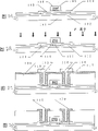
Figure 1A to 1D shows the embodiment of said method, and this is an operation of making thin-film transistor on glass substrate.At first, in the step shown in Figure 1A, form the gate electrode of making by the aluminium that is mixed with scandium 105, form anti-etching mask 106 and 107 then.After this, in electrolyte with forming anode oxide film 108 on the gate electrode 105 of anode oxidation method in not comprising the zone that has hushed up.
After moving, should form in the zone at contact electrode place of gate electrode 105 and form mask 106.In the zone of the gate electrode 105 that will separate after a while, form mask 107.
According to a further aspect in the invention, provide a kind of manufacture method of semiconductor device, it comprises the following steps:
Only form by or main wiring or electrode made of aluminum;
At least in the zone of wiring that will form the contact position after a while or electrode and wanting after a while in the zone at separate wiring or electrode place, form mask;
In electrolyte with the wiring or electrode as anode by carrying out anodic oxidation, form anode oxide film on wiring in not comprising the zone that forms the mask place or the electrode;
Form silicon oxide film so that cover wiring or electrode;
The partial etching silicon oxide film, thus wiring or electrode in the zone that does not form the anode oxide film place exposed;
On total, form metal film; And
To the metal composition, thereby form the contact of wiring or electrode and separately wiring or electrode in different places.
Figure 1A to 1D shows the specific embodiment of said method.Referring to Figure 1A, at first form main gate electrode 105 made of aluminum.Then, in the zone that will form the contact electrode place after a while and in the zone at the gate electrode place that will separate after a while, form mask 106 against corrosion and 107 respectively.After this, form anode oxide film 108 on the gate electrode 105 in the zone of in being not included in electrolyte, covering by anodic oxidation.(Figure 1A)
Then, in step shown in Fig. 1 C, deposition one silicon oxide film 100 as interlayer dielectric.With silicon oxide film 100 partial etchings, just form the contact hole 113 and the window 114 of gate electrode 105.
In this case, form the metal film 117 that constitutes contact electrode and wiring.Form mask against corrosion 118 then to metal film 117 compositions.(Fig. 1 C)
After this, by etching, promptly metal film 117 compositions are formed the contact of gate electrode 105.Simultaneously, by remove with etching window 114 zones in metal film 117 and gate electrode 105 and gate electrode is separated.(Fig. 1 D)
The example of the etching agent of etching oxidation silicon fiml 100 usefulness is for example hydrofluoric acid, buffered hydrofluoric acid (BHF), the hydrofluoric acid that is mixed with acetic acid or a buffered hydrofluoric acid of hydrofluoric acid type etching agent, and these hydrofluoric acid type etching agents have added surface-active agents.A kind of example of buffered hydrofluoric acid is the mixture of ammonium fluoride and hydrofluoric acid (10: 1).These hydrofluoric acid type etching agents are compared the much higher of silicon to the etching rate of silica and aluminium.Therefore, they optionally remove a kind of by or the member mainly made by silica or aluminium, or be of great use when in this member, forming contact hole.
Another kind of way is to use for example CF
4Or CHF
3Fluorine type gas carry out dry etching.
Another aspect again according to the present invention provides a kind of method of making semiconductor device, and it comprises the following steps:
On semiconductor, form dielectric film;
Only on dielectric film, form by or main wiring or electrode made of aluminum;
At least in the zone of wiring that will form the contact position after a while or electrode and in the zone of the wiring that will separately locate after a while or electrode, form mask;
In electrolyte, carry out anodic oxidation to form anode oxide film on wiring in not comprising the zone that forms the mask place or the electrode as anode with wiring or electrode;
Remove this mask;
Form dielectric film, to cover wiring or electrode;
Form the contact hole that semiconductor and wiring or electrode are used simultaneously, and in the zone that will separately locate after a while, expose wiring or electrode;
On whole surface, form metal film; And
To the metal film composition, thereby form the contact of wiring or electrode, and in the zone of such intention is arranged, will connect up or electrode separates.
Another aspect according to the present invention provides a kind of method of making semiconductor device, and it comprises the following steps:
Only form by or main wiring or electrode made of aluminum;
Use wiring or electrode in electrolyte, to carry out anodic oxidation, on wiring that does not comprise its presumptive area or electrode, to form anode oxide film as anode; And
Form the contact electrode of the fate of wiring or electrode, and remove the part of wiring or electrode simultaneously.
It should be noted that the present invention can point be used for making is not only film and partly leads, and also can be general MOS transistor.
According to the present invention, in the anodic oxidation step, by only by or main wiring made of aluminum or electrode on or form anodic oxide coating near it, selections district is foreclosed forming mask in advance, the contact hole of above-mentioned wiring of formation or electrode in step subsequently easily.As a result, its anode oxide film be only by or main wiring made of aluminum or electrode on and near the productivity ratio and the output of the semiconductor device that forms can be improved greatly.
In addition, also by mask method, in the above-mentioned steps of the formation mask before above-mentioned anodic oxidation step, form a kind of like this zone, the gate electrode of a plurality of thin-film transistors in this district will be separated from each other after a while, and this district can prevent to be covered by anode oxide film.In the step that forms wiring and electrode subsequently with composition, also can realize etching in this district.As a result, do not need independent step that gate electrode is separated from each other.
Figure 1A to 1D, Fig. 2 A to 2D, Fig. 3 A to 3D and Fig. 4 A to 4D are the cross sectional view according to the manufacturing thin-film transistor operation of first embodiment of the invention;
Fig. 5 A to 5D is the cross sectional view of the manufacturing thin-film transistor operation of routine;
Fig. 6 A and 6B are the zoomed-in view of the contact hole shown in Fig. 5 D;
Fig. 7 is the circuit pattern of a routine thin-film transistor;
Fig. 8 is the circuit diagram corresponding to Fig. 7;
Fig. 9 A and 9B and Figure 10 A and 10B are the top view according to the manufacturing thin-film transistor operation of first embodiment of the invention; And
Figure 11 A and 11B are the cross sectional view according to the manufacturing thin-film transistor operation of second embodiment of the invention.
Present embodiment is characterised in that, has in the thin-film transistor of main gate electrode made of aluminum in formation, and anodic oxide coating is not formed in that this part is the contact portion as gate electrode on a part of gate electrode.This embodiment also has and is characterised in that, even when forming a plurality of thin-film transistors also as the contact electrode in formation source/drain region or wiring as the contact electrode of gate electrode or the necessary step of wiring, also be the step that gate electrode is separated from each other.
Figure 1A to 1D, Fig. 2 A to 2D, Fig. 3 A to 3D and Fig. 4 A to 4D have showed the manufacturing process according to this embodiment.Fig. 2 A to 2D is the cross sectional view of taking from along A-A ' line of Figure 1A.Fig. 2 A to 3D is the cross sectional view of taking from along B-B ' line of Figure 1A.Fig. 4 A to 4D is the cross sectional view of taking from along C-C ' line of Figure 1A.Figure 1A, 2A, 3A and 4A are corresponding each other, and Figure 1B, 2B, 3B and 4B are corresponding each other, or the like.
At first, the former silicon oxide film 102 of 3,000 is deposited on the glass substrate 101 with plasma CVD method as the prime coat layer film.Though use glass substrate because of being assumed to the operation of producing active matrix liquid crystal display device in the present embodiment, dielectric substrate that other are suitable for or the substrate with insulating surface also can use.
On prime coat layer film 102, deposit the former amorphous silicon film of 500 with plasma CVD method or low pressure hot CVD method.This amorphous silicon film is a starting film, and in order to form the active layer of calculated thin-film transistor, the active layer here is a semiconductor layer, has formed source/drain region and channel formation region in the layer.
Make the amorphous silicon film crystallization by heating or with laser radiation then.In this embodiment, crystal silicon film forms with the laser radiation of KrF excimer.The crystal silicon film of Xing Chenging is patterned into the active layer 103 of thin-film transistor like this.Fig. 9 A is the top view of active layer 103 in this case.
Has only an active layer 103 though Fig. 9 A shows, but with hundreds of to hundreds of thousands or the corresponding active layer 103 of more thin-film transistors, be in the pixel region and peripheral drive circuit of producing active matrix liquid crystal display device, form simultaneously by composition on the glass substrate 101 of tens centimetres of tens cm x.
After active layer 103 forms, deposit the thick silicon oxide film 104 of 1,000 as gate insulating film with plasma CVD method.After this deposited by electron beam evaporation or sputtering method deposition become the thick film of 5,000 main made of aluminum of gate electrode.For preventing the misgrowth of aluminium, scandium is sneaked in the above-mentioned film with 0.1Wt%.
Then main film made of aluminum is patterned into gate electrode 105.This gate electrode (also being called grating routing) 105 is called the ground floor wiring.
On gate electrode 105, form mask 106 against corrosion and 107 then.Next step forms the contact hole of gate electrode 105 in the zone that forms mask against corrosion.In the zone that forms mask against corrosion 107 places, carry out separating of gate electrode after a while.
Then, in electrolyte, form the layer 108 that the oxide of main material made of aluminum is made with anode oxidation method.The thickness setting of oxide layer 108 is 2,000 .In the present embodiment, the pH value is used as electrolyte through the ethylene glycol solution that ammonia is adjusted to neutrality.
In this anodic oxidation step, do not contacted electrolyte by the part of mask 106 against corrosion and 107 gate electrodes 105 that cover, so locate not carry out oxidation, do not form oxide layer 108 on it yet.
So, can get the situation shown in Figure 1A, 2A, 3A and the 4A.Fig. 9 B is the top view of this situation.The cross section of Fig. 2 A is obtained along the line D-D ' among Fig. 9 B, and the cross section of Figure 1A is obtained along the line E-E ' among Fig. 9 B, and the cross section of Fig. 3 A is obtained along the line F-F ' of Fig. 9 B, and the cross section of Fig. 4 A is obtained along the line G-G ' among Fig. 9 B.
After the anodic oxidation step is finished, remove mask 106 against corrosion and 107.Implanted dopant is with formation source/drain region then.In this embodiment, form the N channel thin-film transistor.With plasma doping to inject P (phosphorus) ion.(Figure 1B, 2B, 3B and 4B).
Injection with the P ion forms source region 109 and drain region 112.Form channel formation region 111 and skew grid region 110 simultaneously.
Afterwards, use TEOS gas, deposit the thick silicon oxide film of one deck 2,000 as interlayer dielectric by plasma CVD method.Shown in Fig. 2 C, form the contact hole 115 and 116 in source region 109 and drain region 112 then respectively.Shown in Fig. 1 C and 3C, form the contact hole 113 of gate electrode 105 simultaneously, and, remove a part of silicon oxide film 100 in spaced apart regions by shown in Fig. 1 C and 4C.That is form contact hole 113,115 and 116 and window 114 simultaneously.
The wet etching of the mixing etching agent by using buffered hydrofluoric acid and acetic acid is finished above-mentioned steps.In this step,, just begin etching oxidation silicon fiml 104 in case finish the etching of silicon oxide film 100 in zone corresponding to contact hole 115 and 116 (seeing Fig. 2 C).With the zone of contact hole 113 (seeing Fig. 3 C) and window 114 (seeing Fig. 4 C) in, just begin etching gate electrode 105 in case finish the etching of silica 100.
Though the silicon oxide film 100 among the figure is drawn as in uneven thickness, because of its its thickness that raise in the zone corresponding to gate electrode 105, so can think that it has homogeneous thickness.
According to measurement, when buffered hydrofluoric acid was used as etching agent, the etching rate of aluminium was about half of silica.The thickness of silicon oxide film 104 is about 1,000 (being 1,500 to the maximum), and the thickness of general gate electrode 105 is greater than 4,000 .Therefore, form under the situation of contact hole 115 and 116 in the etching of above-mentioned steps, with the top etching of gate electrode 105 with silicon oxide film 104.But 105 of gate electrodes are subjected to etching slightly, thereby can not cause the situation shown in Fig. 6 B.
Above-mentioned etch step be on the basis of the etching rate of silica, be applicable to when exposing silicon active layer 103 till.In the above described manner, form the contact hole 113 and the window 114 in bonding pad not of the contact hole 115 and 116 be respectively source region 109 and drain region 112, gate electrode simultaneously.(Fig. 1 C, 2C, 3C and 4C)
Figure 10 A is the top view of this situation, has wherein formed the contact hole 113 and the window 114 in bonding pad not of the contact hole 115 and 116, the gate electrode 105 that are source region 109 and drain region 112 respectively.
The subsequent active layer 113 that exposes in contact hole 115 and 116 exposes gate electrode 105 in contact hole 113 and window 114.
Even the situation of some misalignment occurs when forming contact hole 113, the operation of gained thin-film transistor special problem can not occur yet.Because of in relevant manufacturing operation, allowing error to a certain degree.Because almost be provided with electric current by gate electrode 105, a little little variation of the contact area between gate electrode 105 and extraction electrode thereof not too influences the transistorized operation of gained.
Then deposit a multilayer film 117 of forming by titanium film and aluminium film.This multilayer 117 is to constitute second layer wiring.Why will be with the multilayer film of titanium film and aluminium film, be that prevent may be in the inefficacy that electrically contacts at contact hole 115 and 116 places.Form mask 118 against corrosion then with to multilayer film 117 compositions.So just can obtain than the situation shown in 1C, 2C, 3C and the 4C.
Use BCl this moment
3, Cl
2And SiH
4Mist carry out dry etching to remove the exposed portions serve of multilayer film 117.
In this step, multilayer film 117 compositions that will form by titanium film and aluminium film.The part that is present in the part of the multilayer film 117 in window 114 zones and gate electrode 105 simultaneously is etching in addition all.In this pattern step, just separately with gate electrode 105.That is, carry out the composition of second layer wiring and separating of grid wiring (electrode) 105 simultaneously.
Because use chlorine type etching gas to carry out dry etching, when running into silicon oxide film 104, etching just stops basically.Therefore silicon oxide film 104 can suppress film as etching basically.This is that the etching rate of silicon oxide film is much lower than the etching rate of aluminium and titanium film because with chlorine type gas etching the time.
Above-mentioned etch step can be carried out with wet etching, but at this moment etch step becomes complicated, because of coming etching titanium film and aluminium film with different etching agents.
In said method, formed the contact hole (seeing Fig. 1 D and 3D) of source region 119 and drain region 120 (seeing Fig. 2 D) and gate electrode 105.In addition, gate electrode 105 is separated (seeing Fig. 1 D and 4D) at window 114.Figure 10 B is the top view of this situation.Therefore, finished thin-film transistor.Figure 10 B has showed that early the gate electrode at window 114 places is separated.
Though present embodiment with simplified illustration, has in fact formed the complicated circuit that many thin-film transistors are arranged at the condition of production of single thin-film transistor.Fig. 7 shows the example of the part of sort circuit.Specifically, circuit (phase inverter) shown in Figure 7 has been formed the part of the peripheral drive circuit in the active matrix liquid crystal display device.
Fig. 8 circuit diagram is corresponding to Fig. 7.Wiring 702 among Fig. 7 is corresponding to the gate electrode 105 of Figure 1A to 1D, Fig. 2 A to 2D etc., and electrode 703 among Fig. 7 and 704 gate electrodes corresponding to Figure 1A to 1D, Fig. 2 A to 2D etc.
Among Fig. 7,701 refer to spaced regions.Gate electrode (wiring) 702 is at the mode that regional 701 places are partly removed identical with the mode that gate electrode 105 is done at window 114 (seeing Fig. 1 D, 4D and 10B).
Though Fig. 7 only illustrates the partial circuit figure, in fact constituted complicated circuit, the spaced regions that have a lot of and district 701 the same wherein are provided.
Present embodiment is the remodeling of first embodiment, it is characterized in that, use zone of gate electrode 105 separated windows 114 in first embodiment forms wiring (seeing Fig. 1 D and 10B).
Figure 11 A and 11B are the total structure chart according to present embodiment.Among this embodiment, shown in Figure 11 A, utilized unconnected zone to come shape wiring 1001.Figure 11 B is the cross sectional view of taking from along Figure 11 A center line E-E.
Wiring 1001 can form like this, and it is deposited as the gate electrode 105 of part, and in window 114, separating with part gate electrode 105 with to conducting film 117 compositions the time with mask, with formation contact electrode 121.Gate electrode 105 just is separated when it separates with wiring 1001.
According to the present invention, in the anodic oxidation step, by on the wiring of aluminium wiring or electrode or (ground floor) mainly made of aluminum or the electrode or near the formation anodic oxide coating, so that will select the zone to foreclose by forming mask in advance, just in step subsequently, form the contact (second layer) of above-mentioned wiring or electrode easily.
Since need not to remove be difficult to etching only by or the film (anode oxide film) mainly made by aluminium oxide just can form contact hole, thereby the process of manufacturing thin-film semiconductor device or semiconductor integrated circuit just can be more easy and more stable.The result.Can improve the output of thin-film semiconductor device or semiconductor integrated circuit.
In addition, in the step of above-mentioned formation mask, also by adding mask to the ground floor wiring that will separate after a while or the zone of electrode, in its composition, can second layer wiring or electrode is open.Therefore, the number of pattern step can reduce one.This helps to reduce production costs, and increases output.
Because the present invention narrates in conjunction with best real rapid example, scope of the present invention should not be limited on disclosed those instantiations of embodiment.Not departing under the claims, can make many remodeling.For example, used aluminium in an embodiment, but other can anodised metal, for example tantalum also can be used for replacing aluminium.Also have,, might use other materials, for example replace silica with silicon nitride as interlevel insulator.
Claims (11)
1. a method of making semiconductor device comprises the following steps:
On an insulating surface of a substrate, form a semiconductor layer;
But near wiring that comprises the anodic oxidation material of described semiconductor layer preparation, between has an insulating barrier;
On will be and on a second portion of the described wiring that described wiring will separately be located, form mask as a first of the described wiring of a contact zone;
The exposing surface of the described wiring of anodic oxidation only, wherein said first and second parts are because of having described mask not by anodic oxidation;
After described anodic oxidation, remove described mask;
By etching to expose first and second parts of described wiring;
After the continuous described etching, on first and second parts of described wiring, form a conducting film; And
To described conducting film composition, formation separates described wiring with first's electrodes in contact of described wiring and at described second portion.
2. method according to claim 1 is characterized in that described wiring comprises aluminium.
3. method according to claim 1 is characterized in that described anodic oxidation is carried out as anode with described wiring in electrolyte.
4. method according to claim 1 is characterized in that, after the described anodic oxidation and before exposing first and second parts of described wiring, removes described mask.
5. method according to claim 1 is characterized in that described semiconductor layer comprises the silicon metal that is formed on the insulating surface.
6. a method of making semiconductor device comprises the following steps:
Prepare a substrate with insulating surface;
On described insulating surface, form a plurality of semiconductor island;
Form dielectric film on each semiconductor island, described dielectric film works to do the transistor gate dielectric film;
Form grid wiring on described substrate, described grid wiring is included in the gate electrode that extends on the described semiconductor island;
On will be and on the second portion of the described grid wiring that described wiring will be spaced, form mask as the first of the described grid wiring of contact zone;
To form anode oxide film thereon, wherein said first and second parts are not because described mask is subjected to described anodizing with the exposing surface anodic oxidation of described grid wiring;
After described anodic oxidation, remove described mask;
At least as mask the ion that mixes is injected described semiconductor island with described grid wiring, in described semiconductor island, to form impurity range;
On described substrate, form interlayer dielectric, be covered with described semiconductor island, described dielectric film and have the described grid wiring of described anode oxide film;
Optionally the described interlayer dielectric of etching so that form the first of the contact hole and the grid wiring of described semiconductor island, and exposes the described second portion of wiring;
On described interlayer dielectric, form conducting film, so that electrically contact the first of semiconductor island and grid wiring by described contact hole;
Carve by selectivity and to select erosion and will describedly lead film and carve composition, forming the electrode of described grating routing and described semiconductor island, and the while separates described grid wiring at described second portion.
7. a method of making semiconductor device comprises the following steps:
But form a grid wiring that comprises the anodic oxidation material on a substrate, described grid wiring comprises a gate electrode near a semiconductor layer;
On the part of described grid wiring, form a mask;
Make the surperficial anodic oxidation of described grid wiring, wherein, owing to there is described mask, the part that is subjected to described mask covering of described grid wiring is not oxidized;
After anodic oxidation, remove described mask;
On described grid wiring, form a dielectric film after removing described mask;
In described dielectric film, open a hole, to expose described grid wiring part;
On described dielectric film He in the described hole, form conducting film; And
To described conducting film composition, when the above wiring of described part disconnects simultaneously, to form interconnection.
8. method according to claim 7 is characterized in that, described semiconductor layer comprises and is formed on a silicon metal on the insulating surface.
9. method according to claim 7 is characterized in that, described interconnection is to be electrically connected to described semiconductor layer.
10. method according to claim 7 is characterized in that, described interconnection is to be electrically connected to described gate electrode.
11. method according to claim 7 is characterized in that, described wiring comprises the material of selecting a group that forms from tantalum and aluminium.
Applications Claiming Priority (2)
| Application Number | Priority Date | Filing Date | Title |
|---|---|---|---|
| JP80755/95 | 1995-03-13 | ||
| JP7080755A JPH08250746A (en) | 1995-03-13 | 1995-03-13 | Manufacture of semiconductor device |
Publications (2)
| Publication Number | Publication Date |
|---|---|
| CN1137170A CN1137170A (en) | 1996-12-04 |
| CN1092840C true CN1092840C (en) | 2002-10-16 |
Family
ID=13727234
Family Applications (1)
| Application Number | Title | Priority Date | Filing Date |
|---|---|---|---|
| CN96102945A Expired - Fee Related CN1092840C (en) | 1995-03-13 | 1996-03-13 | Method of manufacturing semiconductor device |
Country Status (5)
| Country | Link |
|---|---|
| US (1) | US5849604A (en) |
| JP (1) | JPH08250746A (en) |
| KR (1) | KR100309630B1 (en) |
| CN (1) | CN1092840C (en) |
| TW (1) | TW293174B (en) |
Families Citing this family (14)
| Publication number | Priority date | Publication date | Assignee | Title |
|---|---|---|---|---|
| JP3725266B2 (en) * | 1996-11-07 | 2005-12-07 | 株式会社半導体エネルギー研究所 | Wiring formation method |
| AU9652098A (en) * | 1997-11-18 | 1999-06-07 | Mitsubishi Chemical Corporation | Chemical conversion fluid for forming metal oxide film |
| JP4363684B2 (en) | 1998-09-02 | 2009-11-11 | エルジー ディスプレイ カンパニー リミテッド | Thin film transistor substrate and liquid crystal display device using the same |
| US6433473B1 (en) | 1998-10-29 | 2002-08-13 | Candescent Intellectual Property Services, Inc. | Row electrode anodization |
| EP1041641B1 (en) * | 1999-03-26 | 2015-11-04 | Semiconductor Energy Laboratory Co., Ltd. | A method for manufacturing an electrooptical device |
| US7230965B2 (en) * | 2001-02-01 | 2007-06-12 | Cymer, Inc. | Anodes for fluorine gas discharge lasers |
| US6930053B2 (en) * | 2002-03-25 | 2005-08-16 | Sanyo Electric Co., Ltd. | Method of forming grating microstructures by anodic oxidation |
| JP2008511985A (en) * | 2004-08-31 | 2008-04-17 | エージェンシー フォー サイエンス,テクノロジー アンド リサーチ | Nanostructure and method for producing the same |
| JP4237161B2 (en) * | 2005-05-09 | 2009-03-11 | エルピーダメモリ株式会社 | Manufacturing method of semiconductor device |
| US7524713B2 (en) * | 2005-11-09 | 2009-04-28 | Semiconductor Energy Laboratory Co., Ltd. | Manufacturing method of semiconductor device |
| KR20110098844A (en) | 2008-12-23 | 2011-09-01 | 쓰리엠 이노베이티브 프로퍼티즈 컴파니 | Electrical connections for anodized thin film structures |
| US9252053B2 (en) | 2014-01-16 | 2016-02-02 | International Business Machines Corporation | Self-aligned contact structure |
| CN104461142B (en) * | 2014-12-10 | 2017-06-30 | 京东方科技集团股份有限公司 | Touch display substrate and preparation method thereof, touch control display apparatus |
| CN104966674A (en) * | 2015-07-09 | 2015-10-07 | 京东方科技集团股份有限公司 | Preparation method of thin film transistor, preparation method of array substrate and related devices |
Citations (2)
| Publication number | Priority date | Publication date | Assignee | Title |
|---|---|---|---|---|
| JPH02210420A (en) * | 1989-02-10 | 1990-08-21 | Hitachi Ltd | Production of liquid crystal panel |
| US5146301A (en) * | 1987-10-15 | 1992-09-08 | Sharp Kabushiki Kaisha | Terminal electrode structure of a liquid crystal panel display |
Family Cites Families (7)
| Publication number | Priority date | Publication date | Assignee | Title |
|---|---|---|---|---|
| US4879219A (en) * | 1980-09-19 | 1989-11-07 | General Hospital Corporation | Immunoassay utilizing monoclonal high affinity IgM antibodies |
| JPH0816758B2 (en) * | 1989-02-17 | 1996-02-21 | 松下電器産業株式会社 | Liquid crystal image display device and method of manufacturing the same |
| JPH0772780B2 (en) * | 1989-03-06 | 1995-08-02 | 日本電気株式会社 | Thin film transistor array substrate |
| JP3009438B2 (en) * | 1989-08-14 | 2000-02-14 | 株式会社日立製作所 | Liquid crystal display |
| US5576225A (en) * | 1992-05-09 | 1996-11-19 | Semiconductor Energy Laboratory Co., Ltd. | Method of forming electric circuit using anodic oxidation |
| US5532853A (en) * | 1993-03-04 | 1996-07-02 | Samsung Electronics Co., Ltd. | Reparable display device matrix for repairing the electrical connection of a bonding pad to its associated signal line |
| KR950019817A (en) * | 1993-12-17 | 1995-07-24 | 이헌조 | Moisture prevention pad of liquid crystal module |
-
1995
- 1995-03-13 JP JP7080755A patent/JPH08250746A/en active Pending
-
1996
- 1996-02-29 TW TW085102442A patent/TW293174B/zh not_active IP Right Cessation
- 1996-03-11 US US08/613,372 patent/US5849604A/en not_active Expired - Fee Related
- 1996-03-13 CN CN96102945A patent/CN1092840C/en not_active Expired - Fee Related
- 1996-03-13 KR KR1019960007150A patent/KR100309630B1/en not_active IP Right Cessation
Patent Citations (2)
| Publication number | Priority date | Publication date | Assignee | Title |
|---|---|---|---|---|
| US5146301A (en) * | 1987-10-15 | 1992-09-08 | Sharp Kabushiki Kaisha | Terminal electrode structure of a liquid crystal panel display |
| JPH02210420A (en) * | 1989-02-10 | 1990-08-21 | Hitachi Ltd | Production of liquid crystal panel |
Also Published As
| Publication number | Publication date |
|---|---|
| JPH08250746A (en) | 1996-09-27 |
| TW293174B (en) | 1996-12-11 |
| KR100309630B1 (en) | 2002-06-20 |
| CN1137170A (en) | 1996-12-04 |
| US5849604A (en) | 1998-12-15 |
Similar Documents
| Publication | Publication Date | Title |
|---|---|---|
| CN1222043C (en) | Plate display and its making process | |
| CN1051882C (en) | Semiconductor device and method for forming the same | |
| CN1092840C (en) | Method of manufacturing semiconductor device | |
| CN1260817C (en) | Semiconductor device contg. insulated grid field transistor, and its mfg. method | |
| CN1041973C (en) | A semiconductor device and a manufacturing method thereof | |
| CN1055790C (en) | Semiconductor device and method for manufacturing the same | |
| CN1140900A (en) | Monolithic high frequency integrated circuit structure and method of manufacturing the same | |
| CN100339973C (en) | Method and fabricating semiconductor device | |
| CN1145208C (en) | Semiconductor device and making method thereof | |
| CN101038874A (en) | Method for forming silicon oxide film and for manufacturing capacitor and semiconductor device | |
| CN1507055A (en) | Integrated circuit capacitor | |
| CN1623236A (en) | A method of forming a metal pattern and a method of fabricating tft array panel by using the same | |
| CN1135425C (en) | Manufacturing method of display device | |
| CN1201376C (en) | Manufacturing method for semiconductor device | |
| CN1310339C (en) | Thin-film transistor and producing method thereof | |
| CN1118872C (en) | Semiconductor device and manufacturing method thereof | |
| CN1487569A (en) | Method for producing thin film transistor | |
| CN1320653C (en) | Semiconductor IC device | |
| CN1574293A (en) | Method of manufacturing semiconductor integrated circuit device, and semiconductor integrated circuit device made by its method | |
| CN1819126A (en) | Method of manufacturing semiconductor device having side wall spacers | |
| CN1097311C (en) | Semiconductor device and method for fabricating the same | |
| CN1815754A (en) | Semiconductor device structure and manufature method thereof | |
| CN1248318C (en) | Electronic device with non-luminous display | |
| CN1848392A (en) | Semiconductor device and method of manufacture | |
| CN1487596A (en) | Semiconductor device and producing method thereof |
Legal Events
| Date | Code | Title | Description |
|---|---|---|---|
| C06 | Publication | ||
| PB01 | Publication | ||
| C10 | Entry into substantive examination | ||
| SE01 | Entry into force of request for substantive examination | ||
| C14 | Grant of patent or utility model | ||
| GR01 | Patent grant | ||
| C17 | Cessation of patent right | ||
| CF01 | Termination of patent right due to non-payment of annual fee |
Granted publication date: 20021016 Termination date: 20130313 |