CN1090373C - Terminal and a method of forming the same - Google Patents
Terminal and a method of forming the same Download PDFInfo
- Publication number
- CN1090373C CN1090373C CN95106511A CN95106511A CN1090373C CN 1090373 C CN1090373 C CN 1090373C CN 95106511 A CN95106511 A CN 95106511A CN 95106511 A CN95106511 A CN 95106511A CN 1090373 C CN1090373 C CN 1090373C
- Authority
- CN
- China
- Prior art keywords
- terminal
- scolding tin
- flange
- solder surface
- suppressing portion
- Prior art date
- Legal status (The legal status is an assumption and is not a legal conclusion. Google has not performed a legal analysis and makes no representation as to the accuracy of the status listed.)
- Expired - Fee Related
Links
Images


Classifications
-
- H—ELECTRICITY
- H01—ELECTRIC ELEMENTS
- H01R—ELECTRICALLY-CONDUCTIVE CONNECTIONS; STRUCTURAL ASSOCIATIONS OF A PLURALITY OF MUTUALLY-INSULATED ELECTRICAL CONNECTING ELEMENTS; COUPLING DEVICES; CURRENT COLLECTORS
- H01R4/00—Electrically-conductive connections between two or more conductive members in direct contact, i.e. touching one another; Means for effecting or maintaining such contact; Electrically-conductive connections having two or more spaced connecting locations for conductors and using contact members penetrating insulation
- H01R4/02—Soldered or welded connections
- H01R4/028—Soldered or welded connections comprising means for preventing flowing or wicking of solder or flux in parts not desired
-
- H—ELECTRICITY
- H01—ELECTRIC ELEMENTS
- H01C—RESISTORS
- H01C7/00—Non-adjustable resistors formed as one or more layers or coatings; Non-adjustable resistors made from powdered conducting material or powdered semi-conducting material with or without insulating material
- H01C7/02—Non-adjustable resistors formed as one or more layers or coatings; Non-adjustable resistors made from powdered conducting material or powdered semi-conducting material with or without insulating material having positive temperature coefficient
- H01C7/028—Non-adjustable resistors formed as one or more layers or coatings; Non-adjustable resistors made from powdered conducting material or powdered semi-conducting material with or without insulating material having positive temperature coefficient consisting of organic substances
-
- H—ELECTRICITY
- H01—ELECTRIC ELEMENTS
- H01R—ELECTRICALLY-CONDUCTIVE CONNECTIONS; STRUCTURAL ASSOCIATIONS OF A PLURALITY OF MUTUALLY-INSULATED ELECTRICAL CONNECTING ELEMENTS; COUPLING DEVICES; CURRENT COLLECTORS
- H01R12/00—Structural associations of a plurality of mutually-insulated electrical connecting elements, specially adapted for printed circuits, e.g. printed circuit boards [PCB], flat or ribbon cables, or like generally planar structures, e.g. terminal strips, terminal blocks; Coupling devices specially adapted for printed circuits, flat or ribbon cables, or like generally planar structures; Terminals specially adapted for contact with, or insertion into, printed circuits, flat or ribbon cables, or like generally planar structures
- H01R12/50—Fixed connections
- H01R12/51—Fixed connections for rigid printed circuits or like structures
- H01R12/55—Fixed connections for rigid printed circuits or like structures characterised by the terminals
- H01R12/58—Fixed connections for rigid printed circuits or like structures characterised by the terminals terminals for insertion into holes
-
- H—ELECTRICITY
- H01—ELECTRIC ELEMENTS
- H01R—ELECTRICALLY-CONDUCTIVE CONNECTIONS; STRUCTURAL ASSOCIATIONS OF A PLURALITY OF MUTUALLY-INSULATED ELECTRICAL CONNECTING ELEMENTS; COUPLING DEVICES; CURRENT COLLECTORS
- H01R43/00—Apparatus or processes specially adapted for manufacturing, assembling, maintaining, or repairing of line connectors or current collectors or for joining electric conductors
- H01R43/02—Apparatus or processes specially adapted for manufacturing, assembling, maintaining, or repairing of line connectors or current collectors or for joining electric conductors for soldered or welded connections
- H01R43/0256—Apparatus or processes specially adapted for manufacturing, assembling, maintaining, or repairing of line connectors or current collectors or for joining electric conductors for soldered or welded connections for soldering or welding connectors to a printed circuit board
-
- H—ELECTRICITY
- H05—ELECTRIC TECHNIQUES NOT OTHERWISE PROVIDED FOR
- H05K—PRINTED CIRCUITS; CASINGS OR CONSTRUCTIONAL DETAILS OF ELECTRIC APPARATUS; MANUFACTURE OF ASSEMBLAGES OF ELECTRICAL COMPONENTS
- H05K3/00—Apparatus or processes for manufacturing printed circuits
- H05K3/30—Assembling printed circuits with electric components, e.g. with resistors
- H05K3/306—Assembling printed circuits with electric components, e.g. with resistors with lead-in-hole components
- H05K3/308—Adaptations of leads
-
- H—ELECTRICITY
- H05—ELECTRIC TECHNIQUES NOT OTHERWISE PROVIDED FOR
- H05K—PRINTED CIRCUITS; CASINGS OR CONSTRUCTIONAL DETAILS OF ELECTRIC APPARATUS; MANUFACTURE OF ASSEMBLAGES OF ELECTRICAL COMPONENTS
- H05K3/00—Apparatus or processes for manufacturing printed circuits
- H05K3/30—Assembling printed circuits with electric components, e.g. with resistors
- H05K3/32—Assembling printed circuits with electric components, e.g. with resistors electrically connecting electric components or wires to printed circuits
- H05K3/34—Assembling printed circuits with electric components, e.g. with resistors electrically connecting electric components or wires to printed circuits by soldering
- H05K3/3447—Lead-in-hole components
Landscapes
- Engineering & Computer Science (AREA)
- Microelectronics & Electronic Packaging (AREA)
- Ceramic Engineering (AREA)
- Physics & Mathematics (AREA)
- Electromagnetism (AREA)
- Manufacturing & Machinery (AREA)
- Multi-Conductor Connections (AREA)
- Manufacturing Of Electrical Connectors (AREA)
- Coupling Device And Connection With Printed Circuit (AREA)
Abstract
The invention provides a terminal and a method for manufacturing it in which the adhering range of a solder is optimized to enhance the reliability of solder connecting. A flange to be connected to a member subjected to fixation (printed board) by a solder is formed together with a fixing part to fix a terminal body to the member subjected to fixation. The flange has a soldering surface opposed to the connecting surface (conductor pattern) of the member subjected to fixation on the circumferential surface part side, and also a solder adhesion suppressing part for limiting the solder adhering range of the soldering surface.
Description
The present invention relates to be used for the terminal and the manufacture method thereof of multiple electric, electronic installation such as electric acoustic converter and other parts.
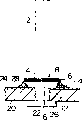
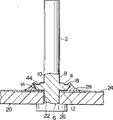
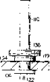
Figure 10 illustrates the structure of the terminal of conventional electro-magnetic acoustic exchanger.This electro-magnetic acoustic exchanger is used for buzzer etc., and printed circuit board (PCB) 104 is installed in the armouring shell 102.Pair of terminal 106 is fixed on this printed circuit board (PCB) 104, and each terminal 106 utilizes scolding tin 108 to be electrically connected with wiring conductor on the printed circuit board (PCB) 104 respectively.Each terminal 106 constitutes input terminals, in order to electro-magnetic acoustic exchanger is applied as the AC signal of drive signal etc.
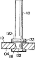
Each terminal 106 is for example used terminal such shown in Figure 11 A always so far.Its large-diameter portion 112 of this terminal is formed on the mid portion of the rear end of cylindrical terminal bodies 110, and its conductive coating 116 is formed on the surface of base material 114.Large-diameter portion 112 shown in Figure 11 B, is pressed into and is fixed on the open-work 118 that is arranged on the printed circuit 104.Conductor fig 119 is formed on the surface of printed circuit board (PCB) 104, and terminal bodies 110 and conductor fig 119 are electrically connected with scolding tin 108 shown in Figure 11 C.But scolding tin 108 can be crossed area extension shown in a often produces scolding tin to the b zone leg.Produce the position expansion that such scolding tin leg adheres to scolding tin, its scope descends the quality of product because factors such as temperature, flatiron characteristic, operator are extremely unstable, becomes the reason that influences product slimmings such as electro-magnetic acoustic exchanger.This also becomes the reason that the outside scolding tin allowed band that connects the terminal bodies 110 of usefulness diminishes.And such terminal only fixes with the open-work 118 that its large-diameter portion 112 inserts printed circuit board (PCB) 104, and the constant intensity of printed circuit board (PCB) 104 is low relatively, thereby the defective of less reliable is arranged.
And terminal shown in Figure 12 is that fixed part 122 is formed on the mid portion of terminal bodies 110 together with flange 120.Also form conductive coating 116 on the surface of its material 114 of this terminal.Such terminal is shown in Figure 12 B, and fixed part 122 inserts printed circuit board (PCB) 104, with flange 120 terminal bodies 110 is positioned vertically within on the printed circuit board (PCB) 104, damages the end of fixed part 122 by pressure fixing back and connects with scolding tin 108.With terminal easy location is arranged, with the constant intensity advantages of higher of printed circuit board (PCB) 104 with such flange 120.But when promptly using such terminal to carry out solder with flatiron, shown in Figure 12 C, the periphery that also produces scolding tin 108 ' surpass flange 120 is attached to the so-called scolding tin leg of terminal bodies 110 sides.Such scolding tin 108 ' be unwanted, it also becomes the grade that makes product and descends, hinders the product slimming.Make the thin reason of scolding tin 108 in the place that needs scolding tin originally.This scolding tin 108 ' the shaping of adhering to terminal be processed with confidential relation.Figure 13 illustrates the processing technology of terminal in the conventional manufacture method.The material of terminal is to use the base material 114 that is bar-shaped, and the conductive coating 116 that is even surface forms in its surface.This terminal material is cut into the length of regulation in advance in conjunction with the processing that is shaped.This base material 114 is put in the finishing die 124,126, carries out press molding and handle in its cavity 128,130.Successively as can be known referring to the skill of science and engineering herein, in Figure 13 A stage, the mid portion of compressed base material 114 is produced in order to forming the expansion of flange 120, owing to be shaped slowly, so the conductive coating 116 on surface is also along the superficial expansion of flange 120 in this stage.After this stage, in case carry out the shaping processing in Figure 13 B stage, facial conductive coating 116 just produced and broke 120 weeks of flange.Expose base material 114 on its all face.And, shown in Figure 12 A, form the terminal that its flange 120 surrounding wall portion produce base material 114 exposed divisions 132 in the final stage shown in Figure 13 C.Such base material 114 exposed divisions 132 are non-even surface, thereby the scolding tin wettability is degenerated.
Must not dare not or would not speak up, yes for conductive coating 116 in order to improving the means of scolding tin wettability, and the base material 114 from then on part exposed of conductive coating 116 is an exposed division 132, and its scolding tin wettability significantly reduces.As a result, shown in Figure 12 C, more than half scolding tin flows to scolding tin 108 ' side, and product grade is descended, and becomes the reason that generation makes scolding tin 108 bad connections.
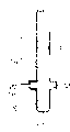
Terminal 106 also used the terminal of such form shown in Figure 14 A in the past.This terminal is step-like flange 134,136 in the mid portion formation of its terminal bodies 110.Conductive coating 116 also is formed on the surface of base material 114 in this terminal.During with such terminal, as shown in Figure 14B, its fixed part 122 inserts printed circuit board (PCB) 104, be positioned to vertical configuration with flange 134, because can be with the end compression failure of fixed part 122, fixing with scolding tin 108 again after fixing, thereby easy location is arranged, with the constant intensity advantages of higher of printed circuit board (PCB) 104.But,, shown in Figure 14 C, be attached to terminal bodies 110 sides around scolding tin 108 ' also can the cross convex line 134,136, and have the defective identical with end shown in Figure 12 even in such terminal.And in this terminal, flange 134,136 is ledge structure, because just the thickness of this part increases, thereby the defective that hinders the terminal miniaturization is arranged.
And, the scolding tin 108 that adheres to like this ' identical with the situation of the terminal of Figure 12.It is its processing technology shown in Figure 15 A, 15B and the 15C.Terminal material is cut into the length of regulation in advance, and this base material 114 is put into finishing die 124,126, carries out press molding in its cavity 128,130.In such formation processing, in processing multistage, be to form flange 134,136, make the mid portion of base material 114 produce expansion in cavity 128,130, the conductive coating 116 on flange 134,136 all faces produces and breaks, and makes its all face expose base material 114.Such base material 114 exposed divisions 138,140 its scolding tin wettabilities are surperficial lower than conductive coating 116, the result, and shown in Figure 14 C, the scolding tin 108 ' high part of the scolding tin wettability of dividing a word with a hyphen at the end of a line diminishes the scolding tin 108 in necessary place, thereby makes the adhesion strength step-down.
High terminal and the manufacture method thereof of reliability that adhering range is optimum, scolding tin connects that the purpose of this invention is to provide a kind of scolding tin.
Terminal of the present invention as shown in Figure 1, it has such structure, promptly form the flange (4) that should be connected with scolding tin (28) and the above-mentioned member that is fixed with the fixed part (6) that terminal bodies (2) is fixed on the member that is fixed (printed circuit board (PCB) 20), this flange facial forms the solder surface (14) relative with the joint face (conductor fig 20) of the above-mentioned member that is fixed in its week, and the scolding tin that forms simultaneously in order to the scolding tin adhering range that limits solder surface adheres to suppressing portion (18).
In terminal of the present invention, if solder surface is relative with the joint face of the member that is fixed, also can become form arbitrarily, for example can be by constituting at all facial inclined plane or the flexure planes that forms of flange.
In terminal of the present invention,, can form recess (annular recess 44 of Fig. 4) or protuberance (annular protrusion 48 of Fig. 8) at the face of the terminal bodies side of flange as the means that prevent that the scolding tin leg from taking place.
In terminal of the present invention, it is to be purpose to suppress that scolding tin adheres to that scolding tin adheres to suppressing portion, and the simplest method can be with non-level and smooth formation.
Scolding tin adheres to suppressing portion can be made the conductive coating (10) that forms on flange peel off to expose base material, forms non-even surface and constitutes.
As shown in Figure 2, the feature of terminal manufacturing method of the present invention is that base material (8) finishing die (30, the 32) press molding by having formed conductive coating on its surface is integrally formed into terminal bodies, flange and fixed part.Simultaneously on above-mentioned flange week face, form solder surface, and make base material expose formation to adhere to suppressing portion in order to the scolding tin of the scolding tin adhering range that limits above-mentioned solder surface from conductive coating.
As mentioned above, in terminal of the present invention, form the fixed part that be fixed on the member that is fixed in terminal bodies one end, simultaneously in the terminal that forms flange owing to facially form the solder surface relative with the joint face of the member that is fixed in the week of this flange, the scolding tin that forms simultaneously in order to restriction scolding tin adhering range adheres to suppressing portion, so scolding tin fully spreads and makes it firm being connected between the solder surface of the joint face of the member that is fixed and flange side, adhere to suppressing portion with scolding tin simultaneously and make scolding tin adhering range unanimity, be suppressed at unwanted and produce scolding tin weldering leg.
In terminal of the present invention, because solder surface, for example be to constitute by the inclined plane or the flexure plane that are positioned on the flange week face, thereby can adhere to the adhering range that suppressing portion combines scolding tin with scolding tin and be limited in the solder surface side, simultaneously because the scolding tin attachment surface is inclined plane or flexure plane, so scolding tin can and the joint face of the member that is fixed between spread reliably, bonding strength improves.
In terminal of the present invention,, the surface distance of flange is increased, thereby can prevent the generation of scolding tin leg reliably owing to form recess or protuberance at the face of the terminal bodies side of flange.
In terminal of the present invention, be non-even surface because scolding tin adheres to suppressing portion, can prevent reliably adhering to of scolding tin, even scolding tin is fully attached on the solder surface.
The conductive coating that is positioned on the flange is peeled off expose base material and can at an easy rate scolding tin be adhered to the non-even surfaceization of suppressing portion, can form the zone of non-cohesive scolding tin selectively.
In terminal manufacturing method of the present invention, by having formed the base material finishing die press molding of conductive coating on its surface, can integrally form terminal bodies, flange and fixed part at an easy rate, can form solder surface and make base material expose the scolding tin that forms in the flange perimembranous and adhere to suppressing portion from conductive coating.
Figure 1A illustrates the face shaping of first embodiment of terminal of the present invention.
Figure 1B is the partial sectional view of expression to the fixed structure of printed circuit board (PCB).
Fig. 1 C is the terminal partial sectional view of expression solder.
Fig. 2 A is the profile of the initial stage forming technology in the manufacture method of terminal shown in the presentation graphs 1.
Fig. 2 B is the profile of expression forming technology in its in mid-term.
Fig. 2 C is its last forming technology of expression and the part sectioned view of finishing product.
Fig. 3 is the amplification profile with the part of the terminal of terminal manufacturing method manufacturing shown in Figure 2.
Fig. 4 is the part sectioned view of the solder among second embodiment of terminal of the present invention.
Fig. 5 A is the profile of the initial stage forming technology of expression terminal manufacturing method shown in Figure 4.
Fig. 5 B is the profile of forming technology in mid-term.
Fig. 5 C is last forming technology and the half-sectional view of finishing product.
Fig. 6 is the profile of the 3rd embodiment of terminal of the present invention.
Fig. 7 is the part sectioned view of solder among the 4th embodiment of expression terminal of the present invention.
Fig. 8 A is the profile of the initial stage forming technology of expression terminal manufacturing method shown in Figure 7.
Fig. 8 B is the profile of expression forming technology in its in mid-term.
Fig. 8 C is the half-sectional view of final forming technology of expression and manufactured goods.
Fig. 9 is the partial sectional view of an embodiment of the expression electro-magnetic acoustic exchanger that uses terminal of the present invention.
Figure 10 is the partial sectional view that the electro-magnetic acoustic exchanger of traditional terminal is used in expression.
Figure 11 A is the part sectioned view of traditional terminal.
Figure 11 B is the partial sectional view of expression terminal to the stationary state of printed circuit board (PCB).
Figure 11 C is the partial sectional view of expression terminal to the scolding tin connection of printed circuit board (PCB).
Figure 12 A is the part sectioned view of the other traditional terminal of expression.
Figure 12 B is the partial sectional view of expression terminal to the printed circuit board (PCB) stationary state.
Figure 12 C is the partial sectional view of expression terminal to the scolding tin connection of printed circuit board (PCB).
Figure 13 A is the profile of the initial stage forming technology in the expression terminal processing technology shown in Figure 12.
Figure 13 B is the profile of expression forming technology in its in mid-term.
Figure 13 C is the half-sectional view of its last forming technology of expression and manufactured goods.
Figure 14 A is a partial sectional view of representing other traditional terminal.
Figure 14 B is the partial sectional view of expression terminal to the stationary state of printed circuit board (PCB).
Figure 14 C is the partial sectional view of expression terminal to the scolding tin connection of printed circuit board (PCB).
Figure 15 A is the profile of the initial stage forming technology in the expression terminal processing technology shown in Figure 14.
Figure 15 B is the profile of expression forming technology in its in mid-term.
Figure 15 C is the half-sectional view of last forming technology of expression and manufactured goods.
Describe the present invention in detail with reference to illustrated embodiment below.
(first embodiment)
Figure 1A, Figure 1B and Fig. 1 C illustrate first embodiment of the invention, and Figure 1A illustrates its face shaping, and Figure 1B is the partial sectional view of expression to the fixed structure of printed circuit board (PCB), and Fig. 1 C is the partial sectional view of expression solder.
Shown in Figure 1A, this terminal has terminal bodies 2, flange 4 and fixed part 6.Terminal bodies 2 and fixed part 6 are identical cylindrical of diameter in the present embodiment.These terminal bodies 2, flange 4 and fixed part 6 are to become integrally to form with identical terminal material, form the conductive coating of being made up of the tin higher than the scolding tin wettability of base material 8, high temperature scolding tin etc. 10 on the surface of base material 8.
On flange 4, smooth stationary plane 12 is arranged on fixed part 6 sides.On its peripheral wall surfaces, form solder surface of forming by the big inclined plane of stationary plane 12 side diameter small terminal main body 2 side diameters and the large-diameter portion 16 that certain width is arranged.Though stationary plane 12 can be set arbitrarily with solder surface 14 angulation θ, because of solder surface 14 constitutes the scolding tin attachment surface, as consider that spreading of scolding tin is the impregnability of scolding tin, then this angle θ is preferably in more than 10 degree.
And on the part of 4 week of flange face, form in order to stop the scolding tin that produces the scolding tin leg to adhere to suppressing portion 18.It is to suppress the part that scolding tin adheres to that this scolding tin adheres to suppressing portion 18, is the means that the adhering range of scolding tin are limited in solder surface 14 sides.Though in this embodiment on the surface of flange 4 with terminal bodies 2 and the fixed part 6 the same conductive coatings 10 that form, but the conductive coating on its part 10 is removed, form the low part of scolding tin wettability forcibly, the part formation scolding tin that exposes with base material 8 adheres to suppressing portion 18.Such scolding tin surface suppressing portion 18 is compared its rough surface with other faces, becomes non-even surface, and this just makes the scolding tin wettability reduce.This is with opposite, and solder surface 14 sides of flange 4 are even surface, its scolding tin wettability height, thereby their scolding tin tack or adhesive force have significant difference.
For making and the member that is fixed inserts fixedly the time easily, form the conical surface 19 in the end of fixed part 6.
Shown in Figure 1B, when using such terminal, the open-work 22 corresponding with fixed part 6 is formed on the printed circuit board (PCB) 20 as the structure member that is fixed.Fixed part 6 inserts this open-work 22, makes the stationary plane 12 of flange 4 and the conductor fig that should fix 24 fluid-tight engagement on the printed circuit board (PCB) 20.One side is kept this state, and one side is in the end conquassation with fixed part 6 of the rear side of printed circuit board (PCB) 20, forms the flange 26 corresponding with flange 4.That is to say by fixed part 6 being inserted the open-work 22 of printed circuit board (PCB) 20, simultaneously printed circuit board (PCB) 20 is held under the arm between flange 4 and flange 26, terminal bodies 2 is fixed on the printed circuit board (PCB) 20.Because of the stationary plane 12 of flange 4 is planes, so stationary plane 12 intersects vertically with terminal bodies 2, and then 2 pairs of printed circuit board (PCB)s 20 of terminal bodies are vertically installed.At this moment, the stationary plane 12 of flange 4 and conductor fig 24 fluid-tight engagement of printed circuit board (PCB) 20, terminal bodies 2 is electrically connected with conductor fig 24.The stationary plane 12 of flange 4 is formed by the male and fomale(M﹠F) beyond the even surface, can also be electrically connected when obtaining mechanical fixation owing to going deep into conductor fig 24 under the situation of male and fomale(M﹠F).Conductor fig 24 usefulness Copper Foils are made, and are close on the printed circuit board (PCB) 20.
Shown in Fig. 1 C, by with flatiron etc. after carrying out solder between the conductor fig 24 of the solder surface 14 of flange 4 and printed circuit board (PCB) 20, scolding tin 28 be the cross-over connection state attached to solder surface 14 and conductor fig 24 between.At this moment because solder surface 14 forms even surface by lip-deep conductive coating 10, the scolding tin wettability improves, so scolding tin 28 spreads to the acute angle-shaped narrow that is formed by solder surface 14 and conductor fig 24, obtains connection status reliably.It is low that scolding tin adheres to suppressing portion 18 its scolding tin wettabilities, stops adhering to of scolding tin 28.That is to say that scolding tin adheres to suppressing portion 18 and finishes the function that solder surface 14 is separated with the face of terminal body 2 sides of flange 4.As a result, adhere to suppressing portion 18 with scolding tin and suppress the generation of scolding tin leg, thereby can prevent of the growth of scolding tin leg reliably to flange 4 upper face sides.And adhering to suppressing portion 18 with scolding tin the scolding tin adhering range is limited in solder surface 14 sides, is that the scolding tin distributed areas are the most suitable thereby can make the adhering range of scolding tin 28.
Fig. 2 A, Fig. 2 B and Fig. 2 C illustrate the manufacture method of terminal shown in Figure 1.
Shown in Fig. 2 A, when making this terminal, use first and second shaping moulds 30,32.Cavity 34 with terminal material external diameter corresponding circle hole shape is arranged on finishing die 30, and the height a of this mould cavity 34 is corresponding with the height of terminal bodies 2.Cavity 36 is formed on the finishing die 32.This cavity 36 has first recess 38 of the truncated cone with inclined plane corresponding with the shape of the flange 4 that will form, and second recess 40 corresponding with fixed part 6, forms the conical surface 42 on recess 40.The height of the degree of depth b of this cavity 36 and flange 4 and fixed part 6 adapts.
When shaping this terminal, in advance conductive coating is worked on the cylindrical substrate 8, and it is cut into the possible length of the shaping of considering flange.After packing into this base material 8 in the cavity 34,36 of finishing die 30,32, exert pressure along direction shown in the arrow P 30,32 of finishing dies and to compress.The part of base material 8 is expanded in recess 38, form prototype flange 4.
Shown in Fig. 2 B, increase the compression stress P of 30,32 of finishing dies, it narrows down at interval, and the shape of pressing recess 38 forms flange 4, and the part of the conductive coating 10 that its week is facial produces be full of cracks, and this part becomes scolding tin and adheres to suppressing portion 18.
As Fig. 2 C and shown in Figure 3, after making its close apposition, 30,32 pressurizations of finishing die just form terminal as product.The recess 38 that is to say flange 4 usefulness cavitys 36 is shaped, and forms large-diameter portion 16, the solder surface 14 that is the inclined plane and stationary plane 12 on its all face, forms scolding tin simultaneously and adheres to suppressing portion 18.
As according to manufacture method can be easily with single base material 8 and finishing die 30,32 and form terminal accurately, and, by a part that forms conductive coating 10 in advance by electroplating processes on the surface of base material 8 is peeled off, can on the side face of flange 4, form the high solder surface 14 of scolding tin wettability selectively and adhere to suppressing portion 18 in order to the scolding tin of restriction scolding tin adhering range.
(second embodiment)
Fig. 4 illustrates second embodiment of terminal of the present invention.Terminal among this second embodiment is to form scolding tin on the part of the cylindrical major diameter part 16 in first embodiment to adhere to suppressing portion 18, promptly with on the face of stationary plane 12 opposite sides forms annular recess 44 at the upper face side of flange 4 simultaneously.
If according to such structure, as shown in Figure 4, the region limits that will adhere to scolding tin 8 is adhered to the generation that suppressing portion 18 and annular recess 44 can suppress the scolding tin leg reliably with scolding tin simultaneously on solder surface 14.
Fig. 5 A, Fig. 5 B and Fig. 5 C illustrate the manufacture method of terminal shown in Figure 4.
Shown in Fig. 5 A, the same with first example, also use finishing die 30,32, the shape of cavity 34,36 also much at one, side that different is in finishing die 30 upper edges below it forms the semicircular protuberance 46 that becomes wall in the cross section of annular.
The manufacturing process of terminal is identical with first embodiment shown in Figure 2.Shown in Fig. 5 A, to pack into base material 8 in the cavity 34,36 and by after the pressurization of the direction shown in the arrow P, the protuberance 46 of finishing die 30 sides begins to enter the prototype section of flange 4, this just causes the be full of cracks of conductive coating 10.So, shown in Fig. 5 B, the be full of cracks of conductive coating 10 partly is that scolding tin adheres to suppressing portion 18 and carries out to upside from solder surface 14, the result, and shown in Fig. 5 C, the bight that forms flange 4 simultaneously promptly is positioned at the annular recess 44 on the upper face side.
When using such finishing die 30, to compare the scolding tin attachment surface with the solder surface 14 of first embodiment and enlarge, scolding tin adheres to the bight side that suppressing portion 18 is displaced to flange 4 simultaneously.Like this, solder surface 14 expansions and scolding tin adhere to the result that suppressing portion 18 is displaced to the angle side.Make the improvement of adhering to of scolding tin 28, can prevent to produce the scolding tin leg reliably simultaneously.When needed, the formation of annular recessed portion 44 makes conductive coating 10 produce be full of cracks effectively, and it produces partly and separates with solder surface 14 sides, and the scolding tin wettability that helps to prevent solder surface 14 degenerates.
(the 3rd embodiment)
Fig. 6 illustrates the 3rd embodiment of terminal of the present invention.Terminal according to second embodiment shown in Figure 4, it is the annular recess 44 that forms bending by the upper face side of flange 4, adhere to suppressing portion 18 and process scolding tin, and in the terminal of this 3rd embodiment, be the periphery of flange 4 to be holded up to the front of terminal 2 form wall portion 5, form the annular recess 45 darker between this wall portion 5 and flange 4 top than the annular recess 44 of second embodiment.And scolding tin adheres to the fore-end that suppressing portion 18 is formed on wall portion 5.
In case after being processed into such structure, the following side of flange 4 and upper face side can be isolated with wall 5, block flowing of scolding tin reliably, and can increase the inhibition effect that scolding tin adheres to suppressing portion 18.
The terminal manufacturing method of this embodiment, the manufacture method with shown in Fig. 5 A-5C forms annular recess 45 as realizing with the protuberance 46 of finishing die 30 sides, promptly can form at an easy rate according to outstanding length corresponding with the degree of depth and shape.Wall portion 5 also can weld and realize with other collar member and terminal.
(the 4th embodiment)
Fig. 7 illustrates the 4th embodiment of terminal of the present invention.The terminal of this 4th embodiment is that scolding tin is adhered to the bight side that suppressing portion 18 is formed on flange 4, and the step that is used in flange 4 upper face sides simultaneously forms the annular protrusion 48 of minor diameter.
If such structure, then the adhering zone of scolding tin 28 is limited in solder surface 14, simultaneously can adhere to the generation that suppressing portion 18 and annular protrusion 48 suppress the scolding tin leg reliably with scolding tin.
Fig. 8 A-8C illustrates the manufacture method of terminal shown in Figure 7.
Shown in Fig. 8 A, use finishing die 30,32, with the difference of first and second embodiment be in the cavity 34 of finishing die 30, to form annular recess 50.
This terminal formation method is identical with second embodiment shown in Figure 4.Shown in Fig. 8 A, base material 8 is packed in the cavity 34,36, pressurize along the direction shown in the arrow P, form the prototype portion of flanges 4 at the recess 38 of finishing die 30,32 and annular recess 50, after further being shaped, shown in Fig. 8 B, at the upper face side formation protuberance 48 of flange 4, simultaneously, the formation of this protuberance 48 impels conductive coating 10 be full of cracks on flange 4 all faces.Like this, shown in Fig. 8 B, the be full of cracks part of conductive coating 10, be that scolding tin adheres to that suppressing portion 18 is also the same with second embodiment in the present embodiment shifts to upside by solder surface 14, the result forms the bight of solder surface 14 simultaneously shown in Fig. 8 C, i.e. the protuberance 48 of side in the above.
When using such finishing die 30, compare with the solder surface 14 of first embodiment, solder surface has enlarged, suppress the scolding tin attachment portion simultaneously and be displaced to the bight, scolding tin adhere to improvement, can prevent to produce the scolding tin leg reliably simultaneously.The same with second embodiment, the effective real estate of the formation of protuberance 48 is given birth to the be full of cracks of conductive coating 10, and this generation part separates with solder surface 14 sides, has enlarged solder surface simultaneously and has helped to prevent that its scolding tin wettability from degenerating.
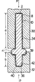
Fig. 9 illustrates the embodiment of the electro-magnetic acoustic exchanger that uses terminal of the present invention.The electro-magnetic acoustic exchanger of this embodiment is to use terminal shown in Figure 7.
Printed circuit board (PCB) 52 is fixed in the armouring shell 51, and terminal T is fixed on this printed circuit board (PCB) 52.Thereby scolding tin 28 spreads between the solder surface 14 of the flange 4 of this terminal T and printed circuit board (PCB) 52, can obtain connection status reliably.And flange 4 is placed on the peristome of sides below the armouring shell 51, and its relative terminal bodies 2 is very little, and this helps the miniaturization and the flattening of sound magnetic acoustic converter as can be known.
Terminal of the present invention enumerates that the example of electromagnetic transducer describes among Fig. 9, but except that such electro-magnetic acoustic exchanger, also can be as the terminal that mixes IC, various electronics, electric device, parts, its application is extensive, the situation that is not limited to embodiment and is exemplified.
The inclined plane of solder surface also can be the flexure plane that relatively is protruding or spill with the joint face of the member that is fixed in an embodiment.
The above embodiment explanation that exemplifies, as use terminal of the present invention or its manufacture method, can obtain following effect.
A. form the fixed part that should be fixed on the member that is fixed as end side in terminal bodies, form the terminal of flange simultaneously, all facing sides at flange form the solder surface relative with the joint face of the member that is fixed, the scolding tin that forms restriction solder surface scope simultaneously adheres to suppressing portion, adhere to the adhering range that suppressing portion limits scolding tin by forming the low scolding tin of scolding tin wettability at scolding tin leg growth part, can make scolding tin that optimal adhering range is arranged, the member that is fixed such as printed circuit board (PCB) can improve with the intensity that scolding tin connects.
B. owing to form by the solder surface of the members that are fixed such as printed circuit board (PCB) and the scolding tin attachment portion that the inclined plane constitutes, connect reliably so scolding tin fully can be soaked into to make, improved the reliability that is connected with scolding tin with the electrical connection of the member that is fixed, the grade that scolding tin is connected improves.
C. and, because the adhering range of scolding tin can suppress the growth of scolding tin leg reliably with the low zone isolation of scolding tin wettability.
D. compare with traditional terminal,, this scope is dwindled, thereby make terminal slimming, the miniaturization of machine, parts can help device, parts slimming, miniaturization because optimal scolding tin adhering range is arranged.
E. and, as with terminal manufacturing method of the present invention, can easily produce terminal with optimal scolding tin adhering range.
When explanation is of the present invention, exemplify out various embodiment feature of the present invention is described, but the invention is not restricted to these embodiment, for realizing purpose of the present invention, should comprise various modified examples.
Claims (8)
1. terminal, it has in order to terminal bodies is fixed to the fixed part and the flange that is connected with the member that is fixed by scolding tin on the member that is fixed, it is characterized in that, said flange forms the solder surface relative with the joint face of the above-mentioned member that is fixed on its all face, the scolding tin that forms simultaneously in order to the scolding tin adhering range that limits above-mentioned solder surface adheres to suppressing portion.
2. according to the said terminal of claim 1, it is characterized in that said solder surface is made of inclined plane or flexure plane on all faces of above-mentioned flange.
3. according to the said terminal of claim 1, it is characterized in that on the face of the above-mentioned terminal bodies side of said flange, forming recess.
4. according to the said terminal of claim 1, it is characterized in that forming to the side-prominent wall portion of the said terminal bodies of said flange, above-mentioned scolding tin adheres to the leading section that suppressing portion is formed on this wall portion.
5. according to the said terminal of claim 1, it is characterized in that on the face of the above-mentioned terminal bodies side of said flange, forming protuberance.
6. according to the said terminal of claim 1, it is characterized in that said scolding tin adheres to suppressing portion and is made of non-even surface.
7. according to the said terminal of claim 1, it is characterized in that it is by the conductive coating that forms is peeled off that said scolding tin adheres to suppressing portion on above-mentioned flange, make it expose base material and form.
8. terminal manufacturing method, it is characterized in that the base material press molding that has been formed with conductive coating on its surface by making with finishing die, be integrally formed into terminal bodies, flange and fixed part, simultaneously on all faces of above-mentioned flange, form solder surface, and base material is exposed from conductive coating, and the scolding tin that forms the scolding tin adhering range of the above-mentioned solder surface of restriction adheres to suppressing portion.
Applications Claiming Priority (2)
| Application Number | Priority Date | Filing Date | Title |
|---|---|---|---|
| JP6128237A JPH07320800A (en) | 1994-05-18 | 1994-05-18 | Terminal and manufacturing method thereof |
| JP128237/94 | 1994-05-18 |
Publications (2)
| Publication Number | Publication Date |
|---|---|
| CN1114458A CN1114458A (en) | 1996-01-03 |
| CN1090373C true CN1090373C (en) | 2002-09-04 |
Family
ID=14979890
Family Applications (1)
| Application Number | Title | Priority Date | Filing Date |
|---|---|---|---|
| CN95106511A Expired - Fee Related CN1090373C (en) | 1994-05-18 | 1995-05-18 | Terminal and a method of forming the same |
Country Status (3)
| Country | Link |
|---|---|
| US (1) | US6049039A (en) |
| JP (1) | JPH07320800A (en) |
| CN (1) | CN1090373C (en) |
Families Citing this family (35)
| Publication number | Priority date | Publication date | Assignee | Title |
|---|---|---|---|---|
| JPH11167944A (en) * | 1997-10-03 | 1999-06-22 | Fujitsu Ltd | I / O pins with solder dam for connection between boards |
| JP3160583B2 (en) * | 1999-01-27 | 2001-04-25 | 日本特殊陶業株式会社 | Resin substrate |
| US6353191B1 (en) * | 1999-12-13 | 2002-03-05 | Fci Americas Technology, Inc. | Column grid array connector |
| JP3550355B2 (en) * | 2000-04-13 | 2004-08-04 | 日本特殊陶業株式会社 | Pin standing board |
| JP2002034125A (en) * | 2000-07-19 | 2002-01-31 | Yazaki Corp | Wiring unit |
| US6552277B1 (en) * | 2000-09-08 | 2003-04-22 | Emc Corporation | Techniques for forming a connection between a pin and a circuit board |
| EP1202390B1 (en) | 2000-10-25 | 2008-05-21 | Japan Aviation Electronics Industry, Limited | An electronic component and a method of manufacturing the same |
| US6716072B1 (en) | 2002-06-27 | 2004-04-06 | Emc Corporation | Systems and methods for disposing a circuit board component on a circuit board using a soldering pin |
| US6773269B1 (en) | 2002-09-27 | 2004-08-10 | Emc Corporation | Circuit board assembly which utilizes a pin assembly and techniques for making the same |
| TWI262627B (en) * | 2003-01-20 | 2006-09-21 | Delta Electronics Inc | Plug structure and forming method |
| US6832917B1 (en) * | 2004-01-16 | 2004-12-21 | Intercon Systems, Inc. | Interposer assembly |
| DE102004006533A1 (en) * | 2004-02-11 | 2005-09-01 | Conti Temic Microelectronic Gmbh | Electrically conductive contact pin for pressing into an opening of a printed circuit board and electrical assembly with such a contact pin |
| US6951467B1 (en) * | 2004-07-08 | 2005-10-04 | The United States Of America As Represented By The Secretary Of The Army | Conductive rivet for circuit card |
| JP4836425B2 (en) * | 2004-09-15 | 2011-12-14 | イビデン株式会社 | Lead pins for semiconductor mounting |
| DE102005062709B4 (en) * | 2005-12-28 | 2009-04-23 | Amphenol-Tuchel Electronics Gmbh | Electrical connection |
| EP1821587B1 (en) * | 2006-02-20 | 2017-08-02 | Denso Corporation | Electronic component mounting structure |
| CN100433221C (en) * | 2006-03-03 | 2008-11-12 | 段沛林 | Prepn. method copper-aluminum composite conductive pole |
| JP2007240235A (en) * | 2006-03-07 | 2007-09-20 | Micronics Japan Co Ltd | Probe and probe assembly for current test |
| JP2010002427A (en) * | 2006-08-09 | 2010-01-07 | Epson Toyocom Corp | Inertial sensor, inertial sensor device and its manufacturing method |
| US20080198565A1 (en) * | 2007-02-16 | 2008-08-21 | Tyco Electronics Corporation | Surface mount foot with coined edge surface |
| US7485017B2 (en) * | 2007-06-05 | 2009-02-03 | Intel Corporation | Pin grid array package substrate including pins having anchoring elements |
| JP2009043844A (en) * | 2007-08-07 | 2009-02-26 | Shinko Electric Ind Co Ltd | Wiring board with lead pins and lead pins |
| KR101060924B1 (en) * | 2009-09-22 | 2011-08-30 | 삼성전기주식회사 | Lead Pins for Package Board |
| JP5350962B2 (en) | 2009-09-30 | 2013-11-27 | 富士通株式会社 | Electronic component, board unit and information processing apparatus |
| JP5009972B2 (en) * | 2009-12-21 | 2012-08-29 | 日立オートモティブシステムズ株式会社 | Connector manufacturing method |
| JP5294355B2 (en) * | 2010-11-09 | 2013-09-18 | 北川工業株式会社 | Contact and contact bonding structure |
| JP5705062B2 (en) * | 2011-08-08 | 2015-04-22 | タイコエレクトロニクスジャパン合同会社 | connector |
| EP3086628B1 (en) * | 2015-04-21 | 2018-07-18 | Braun GmbH | Special electric component, printed circuit board assembly, and method of manufacturing an electric appliance |
| US9634419B2 (en) * | 2015-05-17 | 2017-04-25 | Manzhi Zhou | Cold forming method for forming power pins and power pin formed thereof |
| JP6782096B2 (en) | 2016-05-26 | 2020-11-11 | サンコール株式会社 | Shunt resistor |
| JP6640150B2 (en) * | 2017-06-20 | 2020-02-05 | 矢崎総業株式会社 | Soldering method and soldering structure |
| CN107994341B (en) * | 2017-11-08 | 2021-08-13 | 湖北三江航天险峰电子信息有限公司 | Antenna feed structure |
| CN108598704B (en) * | 2018-03-14 | 2021-04-30 | 湖北三江航天险峰电子信息有限公司 | Microstrip antenna feeder |
| JP7309469B2 (en) * | 2019-06-12 | 2023-07-18 | 新光電気工業株式会社 | Lead pins and wiring boards with lead pins |
| CN116359711A (en) * | 2023-04-11 | 2023-06-30 | 立芯科技(昆山)有限公司 | Adapter |
Family Cites Families (2)
| Publication number | Priority date | Publication date | Assignee | Title |
|---|---|---|---|---|
| DE2820002A1 (en) * | 1978-05-08 | 1979-11-22 | Barke Klaus | Terminal for circuit board - has connecting wires pushed in holes in board with grooves and collars at their tops |
| JP2658672B2 (en) * | 1991-10-11 | 1997-09-30 | 日本電気株式会社 | I/O pin repair structure and repair method |
-
1994
- 1994-05-18 JP JP6128237A patent/JPH07320800A/en active Pending
-
1995
- 1995-05-18 CN CN95106511A patent/CN1090373C/en not_active Expired - Fee Related
-
1997
- 1997-11-24 US US08/976,574 patent/US6049039A/en not_active Expired - Fee Related
Also Published As
| Publication number | Publication date |
|---|---|
| US6049039A (en) | 2000-04-11 |
| CN1114458A (en) | 1996-01-03 |
| JPH07320800A (en) | 1995-12-08 |
Similar Documents
| Publication | Publication Date | Title |
|---|---|---|
| CN1090373C (en) | Terminal and a method of forming the same | |
| CN1290165C (en) | Method for manufacturing semiconductor device | |
| CN1163963C (en) | Lead frame and manufacturing method of resin-encapsulated semiconductor device | |
| CN1237854C (en) | Method for fabricating microwave multifunctional modules using fluoropolymer composite substrates | |
| CN1197292A (en) | Semiconductor device, lead frame, and lead bonding | |
| CN1260795C (en) | Semiconductor device and manufacture thereof, circuit board and electronic machine | |
| CN1108859A (en) | Panel mounting structure and mounting method having extremely fine-pitch electrode terminals | |
| CN1946270A (en) | Printed-wiring board, multilayer printed-wiring board and manufacturing process therefor | |
| CN1460293A (en) | Heat dissipation type BGA package and manufacturing method thereof | |
| CN1206936A (en) | Semiconductor device and manufacturing method thereof | |
| CN1176571A (en) | Multilayer metallized printing plate and its forming module | |
| CN1171167A (en) | Composite intermediate connection element for microelectronic assembly and method for making same | |
| CN1379503A (en) | Electric contact device using resin welding flux, electric connector and connecting method of distributing board | |
| CN1165989C (en) | Semiconductor device and method for manufacturing same | |
| CN1440064A (en) | Semiconductor device and manufacture thereof, circuit board and electronic machine | |
| CN1615069A (en) | Multi-layer printed circuit board and fabricating method thereof | |
| CN1242657C (en) | Improved bonding strength between conductive paste and printed substrate and its production method | |
| CN1521842A (en) | Mounted body of electronic component and manufacturing method thereof | |
| US4580713A (en) | Method for bonding an aluminum wire | |
| WO2005029574A1 (en) | Collet, die bonder, and chip pick-up method | |
| CN1175480C (en) | Semiconductor device and manufacturing method thereof | |
| JP2001177224A (en) | Three-dimensional circuit board and method of manufacturing the same | |
| CN1842915A (en) | Surface mount electronic component and process for manufacturing same | |
| CN1296640A (en) | Anisotropic conductor film, semiconductor chip, and method of packaging | |
| CN1256007C (en) | Laminated ceramic electronic component and manufacturing method thereof |
Legal Events
| Date | Code | Title | Description |
|---|---|---|---|
| C06 | Publication | ||
| PB01 | Publication | ||
| C10 | Entry into substantive examination | ||
| SE01 | Entry into force of request for substantive examination | ||
| C14 | Grant of patent or utility model | ||
| GR01 | Patent grant | ||
| C19 | Lapse of patent right due to non-payment of the annual fee | ||
| CF01 | Termination of patent right due to non-payment of annual fee |