CN1085440C - Small amplitude signal output circuit - Google Patents
Small amplitude signal output circuit Download PDFInfo
- Publication number
- CN1085440C CN1085440C CN98103106A CN98103106A CN1085440C CN 1085440 C CN1085440 C CN 1085440C CN 98103106 A CN98103106 A CN 98103106A CN 98103106 A CN98103106 A CN 98103106A CN 1085440 C CN1085440 C CN 1085440C
- Authority
- CN
- China
- Prior art keywords
- transistor
- output
- output circuit
- power supply
- signal
- Prior art date
- Legal status (The legal status is an assumption and is not a legal conclusion. Google has not performed a legal analysis and makes no representation as to the accuracy of the status listed.)
- Expired - Fee Related
Links
- 230000008859 change Effects 0.000 abstract description 18
- 238000004519 manufacturing process Methods 0.000 abstract description 4
- 230000005540 biological transmission Effects 0.000 description 25
- 230000014509 gene expression Effects 0.000 description 24
- 238000010586 diagram Methods 0.000 description 10
- 230000008901 benefit Effects 0.000 description 6
- 239000000470 constituent Substances 0.000 description 4
- 230000001276 controlling effect Effects 0.000 description 3
- 230000006872 improvement Effects 0.000 description 3
- 230000009467 reduction Effects 0.000 description 3
- 230000007423 decrease Effects 0.000 description 2
- 230000008054 signal transmission Effects 0.000 description 2
- BNPSSFBOAGDEEL-UHFFFAOYSA-N albuterol sulfate Chemical compound OS(O)(=O)=O.CC(C)(C)NCC(O)C1=CC=C(O)C(CO)=C1.CC(C)(C)NCC(O)C1=CC=C(O)C(CO)=C1 BNPSSFBOAGDEEL-UHFFFAOYSA-N 0.000 description 1
- 230000002238 attenuated effect Effects 0.000 description 1
- 230000000694 effects Effects 0.000 description 1
- 230000005674 electromagnetic induction Effects 0.000 description 1
- 238000000034 method Methods 0.000 description 1
- 230000004048 modification Effects 0.000 description 1
- 238000012986 modification Methods 0.000 description 1
- 230000008569 process Effects 0.000 description 1
- 230000001105 regulatory effect Effects 0.000 description 1
- 230000011664 signaling Effects 0.000 description 1
- 230000001629 suppression Effects 0.000 description 1
Images


Classifications
-
- H—ELECTRICITY
- H03—ELECTRONIC CIRCUITRY
- H03K—PULSE TECHNIQUE
- H03K19/00—Logic circuits, i.e. having at least two inputs acting on one output; Inverting circuits
- H03K19/003—Modifications for increasing the reliability for protection
- H03K19/00369—Modifications for compensating variations of temperature, supply voltage or other physical parameters
- H03K19/00384—Modifications for compensating variations of temperature, supply voltage or other physical parameters in field effect transistor circuits
Landscapes
- Physics & Mathematics (AREA)
- Engineering & Computer Science (AREA)
- Computer Hardware Design (AREA)
- Computing Systems (AREA)
- General Engineering & Computer Science (AREA)
- Mathematical Physics (AREA)
- Logic Circuits (AREA)
Abstract
一种小幅度信号的输出电路,它包括一个用于接收逻辑信号而输出小幅度信号的输出部分,该输出部分具有串联在第一电源线和第二电源线之间的第一和第二晶体管,连接在每个电源线和输出部之间的电压控制部分用于减小从输出节点提供的输出电压,因此容许输出部分晶体管的导通电阻较小。晶体管的小导通电阻又会使由生产工序变而引起的输出电路的输出电压的变化变得更小。电压控制部分可具有减小由于温度的变化而引起的输出电路的变化的功能。

An output circuit of a small-amplitude signal, which includes an output section for receiving a logic signal and outputting a small-amplitude signal, the output section having first and second transistors connected in series between a first power supply line and a second power supply line , the voltage control section connected between each power supply line and the output section serves to reduce the output voltage supplied from the output node, thus allowing the on-resistance of the transistor of the output section to be small. The small on-resistance of the transistor will make the change of the output voltage of the output circuit caused by the production process change smaller. The voltage control part may have a function of reducing changes in the output circuit due to changes in temperature.
Description
本发明涉及一种弱放大信号的输出电路,特别是一种通过传输线在集成电路之间传输逻辑信号的小幅度信号的输出电路。The invention relates to an output circuit of a weakly amplified signal, in particular to an output circuit of a small-amplitude signal which transmits a logic signal between integrated circuits through a transmission line.
一些输出电路用作信号传输装置以经过传输通道,例如总线在两个或更多集成电路之间传输信号。在逻辑信号从输出电路将被传输出去时,逻辑信号的逻辑值要假定为高电位(H-level)或为低电位(L-level)。因此,在集成电路的输出电路中,就必需存在一个接收来自集成电路的内部电路的内部逻辑信号的输入端,和一个向另一集成电路传送内部逻辑信号的输出端。Some output circuits are used as signal transmission means to transmit signals between two or more integrated circuits via a transmission channel, such as a bus. When the logic signal is to be transmitted from the output circuit, the logic value of the logic signal is assumed to be a high potential (H-level) or a low potential (L-level). Therefore, in the output circuit of an integrated circuit, there must be an input terminal for receiving an internal logic signal from an internal circuit of the integrated circuit, and an output terminal for transmitting the internal logic signal to another integrated circuit.
虽然绝大多数常用的传输信号具有接近于供给集成电路的电源电位的幅度,但是,近几年信号幅度已被减弱以利于传输。例如,在常用传输信号的CMOS接口的情况下,信号幅度基本上等于电源电位值,例如大约为5V或3V。相反,最近的传输信号具有小幅度,例如用于低电位差分信令(LVDS)接口中,信号幅度为0.3V。信号幅度减小的理由是因为这种减小在信号以较高的速度传输的时候产生优越的效果,功耗越低。噪音越小。因此,就需要以实现高速和/或低功耗为其主要目的集成电路具有一个能够输出较低幅度信号的输出电路。作为输出低幅度信号的装置,已经提出一些建议,下面就是其中的一个例子。Although the vast majority of commonly used transmission signals have amplitudes close to the power supply potentials supplied to integrated circuits, in recent years the signal amplitudes have been attenuated to facilitate transmission. For example, in the case of a CMOS interface which normally transmits signals, the signal amplitude is substantially equal to the value of the power supply potential, for example approximately 5V or 3V. In contrast, recent transmission signals have small amplitudes, such as 0.3V for low level differential signaling (LVDS) interfaces. The reason for the reduction in signal amplitude is that this reduction produces superior results when the signal is transmitted at higher speeds, with lower power consumption. The less noise. Therefore, it is necessary for an integrated circuit whose main purpose is to achieve high speed and/or low power consumption to have an output circuit capable of outputting a relatively low amplitude signal. As a device for outputting a low-amplitude signal, some proposals have been made, and the following is an example of them.
参见图1,它表示作为第一常用输出电路的伪发射极耦合逻辑接口(PECL接口)的电路图,它是一个典型的低幅度接口的例子,该输出电路包括:一PMOS晶体管M11,它有一个与正电位的电源线VDD连接的源极,一个与输出低幅度信号的输出端OUT1连接的漏极和一个与输入端IN1连接的栅极;一NMOS型晶体管M12,它有一个与晶体管M11的漏极连接的漏极,一个与晶体管M11的栅极连接的栅极,和一个与零电位的电源线VSS连接的源极;一终端电阻(终接电阻)RTT1,它具有与输出端OUT1连接的第一端和与终端(终接)电源VTT连接的第二端。Referring to Fig. 1, it represents the circuit diagram as the pseudo-emitter coupled logic interface (PECL interface) of the first commonly used output circuit, and it is the example of a typical low amplitude interface, and this output circuit comprises: a PMOS transistor M11, it has a A source connected to the power supply line VDD of the positive potential, a drain connected to the output terminal OUT1 of the output low-amplitude signal, and a gate connected to the input terminal IN1; an NMOS type transistor M12, which has a connection with the transistor M11 A drain connected to the drain, a gate connected to the gate of the transistor M11, and a source connected to the power supply line VSS of zero potential; a terminating resistor (terminating resistor) RTT1, which has The first terminal and the second terminal connected to the terminal (terminating) power supply VTT.
通常,正电位从集成电路外部供给电源线VDD,而电源线VSS接地。在其他情况下,电源线VDD接地时,负电位就供给电源线VSS。Generally, a positive potential is supplied from outside the integrated circuit to the power supply line VDD, and the power supply line VSS is grounded. In other cases, when the power supply line VDD is grounded, a negative potential is supplied to the power supply line VSS.
端电阻RTT1的值和终端电源电位的值一般按标准给定,其中前者大约为50Ω,后者通过从电源电位VDD中减去大约2V而获得。The value of the terminal resistance RTT1 and the value of the terminal power supply potential are generally given according to the standard, wherein the former is about 50Ω, and the latter is obtained by subtracting about 2V from the power supply potential VDD.
在工作时,当接近于电源线VDD的电位VDD的电位以高电平供给输入端IN1时,晶体管M11截止,而晶体管M12导通。因此,电流路径是从终端电源VTT到电源线VSS,并经过终端电阻RTT1和晶体管M12。在此情况下,输出端OUT1的低电位VOL表达为:In operation, when a potential VDD close to the potential VDD of the power supply line VDD is supplied to the input terminal IN1 at a high level, the transistor M11 is turned off, and the transistor M12 is turned on. Therefore, the current path is from the terminal power supply VTT to the power supply line VSS, and passes through the terminal resistor RTT1 and the transistor M12. In this case, the low potential VOL of the output terminal OUT1 is expressed as:
VOL=VTT-{(VTT-VSS)×RTT}/(RTT+RONN)VOL=VTT-{(VTT-VSS)×RTT}/(RTT+RONN)
………(1), ………(1),
其中VTT,VSS,RTT和RONN分别代表终端电源VTT的电位,电源线VSS的电位,电阻RTT1的阻值和NMOS型晶体管M12的导通阻值。VTT, VSS, RTT and RONN respectively represent the potential of the terminal power supply VTT, the potential of the power line VSS, the resistance of the resistor RTT1 and the conduction resistance of the NMOS transistor M12.
当接近于电源线VSS的电位VSS的电位以低电平供给输入端IN1时,晶体管M11导通,而晶体管M12截止。因此,电流路径是从电源线VDD到终端电源VTT,并经过终端电阻RTT1和晶体管M11形成的。在此情况下,输出端OUT1的高电位值VOH表达为:When a potential VSS close to the potential VSS of the power supply line VSS is supplied to the input terminal IN1 at a low level, the transistor M11 is turned on, and the transistor M12 is turned off. Therefore, a current path is formed from the power supply line VDD to the terminal power supply VTT through the terminal resistor RTT1 and the transistor M11. In this case, the high potential value VOH of the output terminal OUT1 is expressed as:
VOH=VTT+{(VDD-VTT)×RTT}/(RTT+RONP)VOH=VTT+{(VDD-VTT)×RTT}/(RTT+RONP)
………(2), ………(2),
其中RONP表示PMOS型晶体管M11的导通电阻值。Where RONP represents the on-resistance value of the PMOS transistor M11.
为了计算出输出端OUT1的高电位VOH和低电位VOL的实际值和相关的输出信号幅度(VOH-VOL),表达式或方程式(1)和(2)中的每个变量值设定如下:VDD=3V,VSS=0V,RTT=50Ω,RONN=200Ω,RONP=200Ω。In order to calculate the actual values of the high potential VOH and the low potential VOL of the output terminal OUT1 and the associated output signal amplitude (VOH-VOL), the values of each variable in the expressions or equations (1) and (2) are set as follows: VDD=3V, VSS=0V, RTT=50Ω, RONN=200Ω, RONP=200Ω.
在上述数值替换表达式(1)和(2)中的变量之后,输出端OUT的高电位VOH和低电位VOL的值计算如下:After replacing the variables in the expressions (1) and (2) with the above values, the values of the high potential VOH and the low potential VOL of the output terminal OUT are calculated as follows:
VOH=1.8V ………(3)VOH=1.8V ………(3)
VOL=1.2V ………(4)VOL=1.2V ………(4)
因此,输出信号幅度被计算出如下:Therefore, the output signal amplitude is calculated as follows:
VOH-VOL=0.6V ………(5)VOH-VOL=0.6V………(5)
常用的输出电路具有这样的特征:它能够通过选择导通电阻RONP和RONN的阻值获得一所需的小信号幅度,这些阻值是根据集成电路中的晶体管元件的规模,依据事先给定的电源电位值VDD,VSS,VTT和终端电阻RTT调节的。The commonly used output circuit has such a feature: it can obtain a required small signal amplitude by selecting the resistance values of the on-resistance RONP and RONN. Power supply potential values VDD, VSS, VTT and terminating resistor RTT are regulated.
由于第一常用输出电路具有一个传输单信号的单输出端,它一般被称之为单向传输系统。Since the first common output circuit has a single output terminal for transmitting a single signal, it is generally called a one-way transmission system.
作如具有低信号幅度接口的另一个传输系统,即所谓差动传输系统也被使用,它从各自的输出端输出一对传输信号。在该差动传输系统中的这对传输信号具有这样的特征:这对信号的相位相反,具有相同的高电位和低电位。这种差动传输系统中的反相位的设计与单相位传输系统相比提供了一个两倍的动态范围。除此之外,它还具有这样的一个优点:受电源电位中噪音的影响和电磁感应的干扰减少了。从这个优点来看,差动传输系统是能够用于高速和高可靠性传输的。在差动传输系统发送差动信号的输出电路的建议已经提出,下面是其一个例子。As another transmission system with low signal amplitude interfaces, so-called differential transmission systems are also used, which output a pair of transmission signals from respective outputs. The pair of transmission signals in the differential transmission system has such characteristics that the phases of the pair of signals are opposite, and they have the same high potential and low potential. The inverted phase design in this differential transmission system provides a twice the dynamic range compared to a single phase transmission system. In addition to this, it has the advantage that the influence of noise in the power supply potential and interference by electromagnetic induction is reduced. From this advantage, the differential transmission system is capable of high-speed and high-reliability transmission. Proposals have been made for an output circuit for transmitting a differential signal in a differential transmission system, an example of which is shown below.
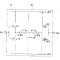
图2表示作为典型的差动传输系统的LVDS接口的第二个常用输出电路,其中相同的组成元件用与图1中使用的同一参考标号表示。该输出电路包括:第一输出部分11,它具有晶体管M11和M12,终端电阻RTT1,输入端IN1和输出端OUT1,它们与第一常用输出电路相同;第二输出部分12,它具有与第一输出部11相同的组成元件。更详细地说,第二输出部分12包括:一PMOS型晶体管M21,它有一个与正电位的电源线VDD连接的源极。一个与输出端OUT2连接的漏极和一个与输入端IN2连接的栅极;一NMOS型晶体管M22,它有一个与晶体管M21的漏极连接的漏极,一个与晶体管M21的栅极连接的栅极,和一个与零电位的电源线VSS连接的源极;一终端电阻RTT2,它具有与输出端OUT2连接的第一端和与端电源VTT连接的第二端。FIG. 2 shows a second conventional output circuit of an LVDS interface which is a typical differential transmission system, in which the same constituent elements as those used in FIG. 1 are denoted by the same reference numerals. This output circuit comprises: a
终端电阻RTT1和RTT2的值,端电源电压值VTT一般按标准给定,其中RTT1和RTT2设定为大约45Ω至65Ω,VTT设定为大约1.1V至1.4V。The values of the terminal resistors RTT1 and RTT2 and the terminal power supply voltage VTT are generally given according to the standard, wherein RTT1 and RTT2 are set to about 45Ω to 65Ω, and VTT is set to about 1.1V to 1.4V.
在工作时,当接近于电源线VDD电位VDD的高电平电位供给输入端IN1时,同时,接近于电源线VSS电位VSS的低电平电位供给输入端IN2时,晶体管M12和M21导通,而晶体管M11和M22截止。因此,电流路径是从电源线VDD经晶体管M21和终端电阻RTT2到端电源VTT形成的另一条电流路径是从端电源VTT到电源线VSS,并经过终端电阻RTT1和晶体管M12形成的。因此,输出端OUT1输出一低电平信号,输出端OUT2输出一高电平信号。高电平信号的电位VOH和低电平信号的电位VOL由上述的表达式(1)和(2)给定。During operation, when a high-level potential close to the VDD potential VDD of the power supply line is supplied to the input terminal IN1, and at the same time, when a low-level potential close to the VSS potential VSS of the power supply line is supplied to the input terminal IN2, the transistors M12 and M21 are turned on, However, transistors M11 and M22 are turned off. Therefore, the current path is formed from the power supply line VDD to the terminal power supply VTT through the transistor M21 and the terminal resistor RTT2, and another current path is formed from the terminal power supply VTT to the power supply line VSS through the terminal resistor RTT1 and the transistor M12. Therefore, the output terminal OUT1 outputs a low level signal, and the output terminal OUT2 outputs a high level signal. The potential VOH of the high-level signal and the potential VOL of the low-level signal are given by the expressions (1) and (2) described above.
当接近于电源线VSS的电位VSS的低电平电位供给输入端IN1时,同时,接近于电源线VDD的电位VDD的高电平电位供给输入端IN2时,晶体管M11和M22导通,而晶体管M12和M21截止。因此,一条电流路径是从电源线VDD到端电源VTT,并经过和终端电阻RTT1晶体管M11形成的,另一条电流路径从端电源VTT到电源线VSS,并经过终端电阻RTT2和晶体管M22形成的。因此,输出端OUT1输出一高电平信号,输出端OUT2输出一低电平信号。When a low-level potential close to the potential VSS of the power supply line VSS is supplied to the input terminal IN1, and at the same time, when a high-level potential close to the potential VDD of the power supply line VDD is supplied to the input terminal IN2, the transistors M11 and M22 are turned on, and the transistor M12 and M21 cut off. Therefore, one current path is formed from the power supply line VDD to the terminal power supply VTT, and passes through the terminal resistor RTT1 transistor M11, and the other current path is formed from the terminal power supply VTT to the power supply line VSS, and passes through the terminal resistor RTT2 and the transistor M22. Therefore, the output terminal OUT1 outputs a high level signal, and the output terminal OUT2 outputs a low level signal.
如上所述,这种在第二常用差动输出系统的输出电路中产生高电平和低电平的输出信号电位的技术方案与第一常用单相系统的输出电路的情况相似。因此,如果表达式(1)和(2)中的变量在两个电路中是相同的话,那么高电平信号VOH和低电平信号VOL的值就等于上述的数值(3),(4)和(5)。在第二常用输出电路中也能够获得所需的小幅度信号,与第一常用输出电路的情况相似,它能够通过选择PMOS型晶体管M11和M21的导通电阻RONP的阻值或NMOS型晶体管M12和M22的RONN的阻值,这些阻值是根据集成电路中的晶体管的规模,依据电源电位VDD,VSS,VTT和事先给定的端电阻RTT的值控制的。As mentioned above, this technical scheme of generating high-level and low-level output signal potentials in the output circuit of the second common differential output system is similar to that of the output circuit of the first common single-phase system. Therefore, if the variables in the expressions (1) and (2) are the same in both circuits, the values of the high-level signal VOH and the low-level signal VOL are equal to the above-mentioned values (3), (4) and (5). The required small-amplitude signal can also be obtained in the second commonly used output circuit, similar to the situation of the first commonly used output circuit, it can be obtained by selecting the resistance value of the on-resistance RONP of the PMOS transistor M11 and M21 or the resistance value of the NMOS transistor M12 and the resistance value of RONN of M22, these resistance values are controlled according to the scale of the transistor in the integrated circuit, according to the power supply potential VDD, VSS, VTT and the value of the terminal resistance RTT given in advance.
虽然两种常用输出电路所具有如上描述的优点,但是它们存在这样一个问题:输出信号幅度的变化是相当大的。Although the two commonly used output circuits have the advantages described above, they have a problem that the variation of the output signal amplitude is considerable.
除此之外,根据控制第一常用输出电路的输出信号的高电平电压值VOH和低电平电压值VOL,下面三种因素也会引起导通电阻RONP和RONN的电阻值的变化。In addition, according to the high-level voltage VOH and the low-level voltage VOL of the output signal controlling the first common output circuit, the following three factors may also cause changes in the resistance values of the on-resistance RONP and RONN.
第一种因素是受MOS晶体管生产工序的变化的影响。生产工序涉及许多变化因素,这些变化因素影响组成输出电路的晶体管元件的形状变化。例如,MOS晶体管的导通电阻根据晶体管的形状,其变化范围一般为10%±至±20%。The first factor is influenced by variations in the MOS transistor production process. The production process involves many variables that affect the shape variations of the transistor elements that make up the output circuit. For example, the on-resistance of a MOS transistor generally varies from 10%± to ±20% depending on the shape of the transistor.
第二种因素是受,装备有集成电路的电子设备用于各种环境下周围环境温度的影响。MOS晶体管的导通电阻特别会随着环境温度的变化而改变:例如,相对于100℃的高温,阻值的变化范围大约为±8%至±16%。The second factor is the influence of ambient temperature in various environments in which electronic equipment equipped with integrated circuits is used. In particular, the on-resistance of a MOS transistor changes with changes in ambient temperature: for example, relative to a high temperature of 100° C., the range of resistance changes is approximately ±8% to ±16%.
第三种因素是受电源电位变化的影响。从集成电路外部供给的电源的电位除了外部电源自身的电位变化外,由于电源线的电位损耗而会产生变化。MOS晶体管的导通电阻随着输入电压的变化而改变:例如,相对于电源电位±10%的变化量,阻值变化范围一般大约为10%±至±15%。The third factor is influenced by the change of the power supply potential. The potential of the power supply supplied from outside the integrated circuit changes due to potential loss of the power supply line in addition to the potential change of the external power supply itself. The on-resistance of the MOS transistor changes with the change of the input voltage: for example, relative to the change of the power supply potential of ±10%, the resistance value generally varies from about 10% to ±15%.
因此,当考虑上述的全部三种因素时,MOS晶体管的导通电阻的变化范围一般大约为±28%至±51%。由三种因素引起的变化导致高电平VOH,低电平VOL和信号幅度的变化范围如下:Therefore, when all three factors mentioned above are considered, the variation range of the on-resistance of a MOS transistor is generally about ±28% to ±51%. Variations caused by three factors lead to high-level VOH, low-level VOL, and signal amplitude ranges as follows:
VOH=1.713V至2.007V ………(6)VOH=1.713V to 2.007V ………(6)
VOL=0.993V至1.287V ………(7)VOL=0.993V to 1.287V ………(7)
VOH-VOL=0.426V至1.014V………(8)VOH-VOL=0.426V to 1.014V......(8)
信号幅度VOH-VOL的变化量是在三种因素不作考虑时,从MOS晶体管的导通电阻计算出的信号幅度的1.7倍,即如表达式(3)所示的0.6V。输出信号幅度的变化量,特别是在较高方向的变化量的情况下,能够减弱和消除上述小幅度传输的优点和效果。The variation of the signal amplitude VOH-VOL is 1.7 times the signal amplitude calculated from the on-resistance of the MOS transistor when the three factors are not considered, that is, 0.6V as shown in the expression (3). Variations in the output signal amplitude, especially in the case of higher directional variations, can reduce and eliminate the advantages and effects of small amplitude transmissions described above.
总而言之,第一和第二常用输出电路存在一个需要解决的信号幅度中较大变化量的问题,引起传输速度降低。在信号传输的过程中引起功耗的增加和噪音的增强。In summary, the first and second conventional output circuits have a problem of a large amount of variation in signal amplitude to be resolved, causing a decrease in transmission speed. In the process of signal transmission, it causes the increase of power consumption and the enhancement of noise.
鉴于上述问题,本发明的目的是提供一种能够解决上述问题的小幅度信号的输出电路。In view of the above problems, the purpose of the present invention is to provide an output circuit for small amplitude signals which can solve the above problems.
本发明提供一种信号输出电路。The invention provides a signal output circuit.
参见附图,本发明的上述和其他目的,特征和优点通过下面的描述将会变得更清楚。The above and other objects, features and advantages of the present invention will become more apparent from the following description with reference to the accompanying drawings.
图1是第一常用输出电路的电路图;Fig. 1 is the circuit diagram of the first common output circuit;
图2是第二常用输出电路的电路图;Fig. 2 is the circuit diagram of the second commonly used output circuit;
图3是本发明第一实施例的输出电路的电路图;Fig. 3 is the circuit diagram of the output circuit of the first embodiment of the present invention;
图4是本发明第二实施例的输出电路的电路图;Fig. 4 is the circuit diagram of the output circuit of the second embodiment of the present invention;
图5是本发明第三实施例的输出电路的电路图;Fig. 5 is the circuit diagram of the output circuit of the third embodiment of the present invention;
图6是本发明第四实施例的输出电路的电路图;Fig. 6 is the circuit diagram of the output circuit of the fourth embodiment of the present invention;
图7是本发明第五实施例的输出电路的电路图;Fig. 7 is the circuit diagram of the output circuit of the fifth embodiment of the present invention;
图8是本发明第六实施例的输出电路的电路图。Fig. 8 is a circuit diagram of an output circuit of a sixth embodiment of the present invention.
现在,参考附图对本发明做更详细地描述,其中全部附图中相同的组成元件用同一或相似的参考标号表示。Now, the present invention will be described in more detail with reference to the accompanying drawings, in which the same constituent elements are denoted by the same or similar reference numerals throughout.
参见图3,它表示本发明第一实施例的输出电路的电路图,该输出电路包括一个第一输出部分11,它设有第一导电型的pMOS型第一晶体管M11和第二导电型的nMOS型第二晶体管M12,一个终端电阻RTT1,一个输入端IN1和一个输出端OUT1,它们与第一常用输出电路的组成元件相同。除此之外,该输出电路还包括一个连接在电源线VDD和晶体管M11的源极之间的一个第一电压控制部分13,它用于控制晶体管M11的电压值。Referring to Fig. 3, it shows the circuit diagram of the output circuit of the first embodiment of the present invention, and this output circuit comprises a
电压控制部分13包括一个nMOS型晶体管M31,它具有与电源线VDD连在一起的一个栅极和一个漏极,以及与输出电路11的晶体管M11的源极连接的源极,因此它形成一个二极管的结构,即,所述二极管是通过漏极和栅极连接在一起的一个MOSFET实现的。The
在工作时,当接近于电源电压VSS电位的信号电位以低电平供给输入端IN1时,那么输出电路的晶体管M11导通,晶体管M12截止,然而电压控制部分13的晶体管M31在任何时候都是导通的。因此,电流路径从电源线VDD经过晶体管M31,晶体管M11和终端电阻RTT1到端电源线VTT而形成。在此情况下,输出端的高电平电压VOH表达为:In operation, when a signal potential close to the potential of the power supply voltage VSS is supplied to the input terminal IN1 at a low level, then the transistor M11 of the output circuit is turned on and the transistor M12 is turned off, while the transistor M31 of the
VOH=VTT+{(VDD-VTN31-VTT)×RTT}/(RTT+RONP)VOH=VTT+{(VDD-VTN31-VTT)×RTT}/(RTT+RONP)
…………(9) …………(9)
其中VTN31表示NMOS晶体管M31的栅源电压。在此组成结构中,输出高电平VOH减少了VTN31×RTT/(RTT+RONP)。在此晶体管M31的导通电阻被忽略不计,这是因为它与晶体管M11的导通电阻RONP相比显得相当小。Where VTN31 represents the gate-source voltage of the NMOS transistor M31. In this composition structure, the output high level VOH is reduced by VTN31×RTT/(RTT+RONP). The on-resistance of transistor M31 is neglected here because it is relatively small compared to the on-resistance RONP of transistor M11.
在本实施例的输出电路中较小输出电压VOH的构成能使晶体管M11的导通电阻RONP在与常用电路中的导通电阻相比时具有更小的绝对值构成。以此能够抑制输出信号的高电平VOH的变化。晶体管M11的导通电阻一般受前述的三种因素的影响而变化,也就是说,受生产工序,环境温度和/或电源电压的影响。The configuration of the smaller output voltage VOH in the output circuit of this embodiment enables the on-resistance RONP of the transistor M11 to have a smaller absolute value configuration when compared with the on-resistance in a conventional circuit. This makes it possible to suppress variations in the high level VOH of the output signal. The on-resistance of the transistor M11 is generally affected by the aforementioned three factors, that is, the production process, ambient temperature and/or power supply voltage.
从确定第一常用输出电路中的输出信号的高电平的表达式(2)可以明白,晶体管M11的导通电阻RONP的减小提高了输出的高电平VOH,它是通过电压控制部13分提供一个电位差抑制的,如上所述并在下文详细地讨论。As can be understood from the expression (2) for determining the high level of the output signal in the first common output circuit, the reduction of the on-resistance RONP of the transistor M11 raises the high level VOH of the output, which is passed through the
电压控制部分13的输出电位,即晶体管M11源极的电位通过从电源电压VDD中减去晶体管M31的栅源电压VTN31获得。当电源电压VDD变化时,电压变化也会照原样在电压控制部分13的输出电位中出现。The output potential of the
如果表达式(9)中的每个变量设定为:VDD=3V,VSS=0V,VTT=1.5V,RTT=50Ω,VTN31=1.0V和RONP=33Ω,本实施例的输出信号的高电平VOH被如下计算:If each variable in expression (9) is set as: VDD=3V, VSS=0V, VTT=1.5V, RTT=50Ω, VTN31=1.0V and RONP=33Ω, the high voltage of the output signal of the present embodiment The flat VOH is calculated as follows:
VOH=1.8V …………………(10)VOH=1.8V …………………(10)
该数值与现有技术中的表达式(3)的值一样。This numerical value is the same as the value of expression (3) in the prior art.
假定晶体管M11的导通电阻RONP受三种因素的影响而变成较大值,输出信号的高电平VOH的变化最大范围如现有技术中所述的一样在±51%内。表达式(9)给出输出信号高电平VOHC的范围如下,其中考虑了变化因素:Assuming that the on-resistance RONP of the transistor M11 becomes larger due to the influence of three factors, the maximum variation range of the high level VOH of the output signal is within ±51% as described in the prior art. Expression (9) gives the range of the output signal high level VOHC as follows, where the variation factors are considered:
VOHC=1.750V至1.878V ………………(11)VOHC=1.750V to 1.878V ……………(11)
因此,高电平VOHC在本实施例中从正常的电压1.8V在-2.8%至+4.8%之间变化,该事实表明与常用的变化范围-4.8%至+11.5%相比有重大的改进。Thus, the fact that the high level VOHC varies between -2.8% and +4.8% from the normal voltage of 1.8V in this example represents a significant improvement over the commonly used range of -4.8% to +11.5% .
在上述实施例中,即使晶体管M11的导通电阻RONP以大百分比变化,由于晶体管M11的导通电阻中的绝对变化与常用电路相比较小,因此输出电位的变化就较小,这种情况通过晶体管M11的导通电阻的绝对值根据晶体管M31的栅源电压降而设定一个较小值来实现。即它能够抑制输出高电平VOH的变化。In the above-described embodiment, even if the on-resistance RONP of the transistor M11 changes by a large percentage, since the absolute change in the on-resistance of the transistor M11 is small compared with a conventional circuit, the change in the output potential is small, which is achieved by The absolute value of the on-resistance of the transistor M11 is realized by setting a smaller value according to the gate-source voltage drop of the transistor M31. That is, it can suppress the change of the output high level VOH.
参考图4,本发明的第二实施例的输出电路与第一实施例相似,它除了电压控制部分14连接在电源线VSS和nMOS晶体管M12的源极之间以控制晶体管M12的源极电压之外。Referring to FIG. 4, the output circuit of the second embodiment of the present invention is similar to the first embodiment, except that the
电压控制部分14包括一个nMOS晶体管M14,它具有与晶体管M12的源极连接在一起的漏极和栅极,和与电源线VSS连接的源极,以此形成一个二极管结构。The
输出电路起到抑制输出信号的低电平VOL变化的作用。具体地说,与第一实施例相似,以较小绝对值选择输出电路11的晶体管M12的导通电阻RONN,使因三个因素的影响造成的导通电阻RCNP的绝对值变化更小。The output circuit plays the role of suppressing the low-level VOL change of the output signal. Specifically, similar to the first embodiment, the on-resistance RONN of the transistor M12 of the
在工作时,当接近于电源电压VDD电位的高电平信号电位供给输入端IN时,那么输出电路11的晶体管M12和M11分别导通和截止,然而电压控制部分14的晶体管M41在任何时候都是导通的。因此,电流路径从端电源VTT经过终端电阻RTT1,晶体管M12和晶体管M41到电源线VSS而形成。在此情况下,输出端的低电平VOL表达为:In operation, when a high-level signal potential close to the potential of the power supply voltage VDD is supplied to the input terminal IN, then the transistors M12 and M11 of the
VOL=VTT+{(VTT-VTN41-VSS)×RTT}/(RTT+RONN)VOL=VTT+{(VTT-VTN41-VSS)×RTT}/(RTT+RONN)
其中VTN41表示NMOS晶体管M41的栅源电压。晶体管M41的导通电阻由于较小被忽略不计。Where VTN41 represents the gate-source voltage of the NMOS transistor M41. The on-resistance of transistor M41 is negligible due to its small size.
从确定第一常用输出电路中的输出低电平VOL的表达式(1)可以明白,如果晶体管M12的导通电阻RONN由于三种因素的影响以较小值变化时,那么输出低电平VOL下降。电压控制部分14提供电位差以此抑制这种下降。From the expression (1) that determines the output low level VOL in the first common output circuit, it can be understood that if the on-resistance RONN of the transistor M12 changes with a small value due to the influence of three factors, then the output low level VOL decline. The
在本实施例中晶体管M14用作电压控制器,电压控制部分14的输出电位通过把晶体管M41的栅源电压VTN41加给电源电压VSS而获得。当电源电压VSS变化时,电压控制部分14的输出电位能够显示变化量。The transistor M14 is used as a voltage controller in this embodiment, and the output potential of the
当表达式(12)中的每个变量设定为:VDD=3V,VSS=0V,VTT=1.5V,RTT=50Ω,VTN31=1.0V和RONN=33Ω,本实施例的输出信号的低电平VOL计算如下:When each variable in the expression (12) is set as: VDD=3V, VSS=0V, VTT=1.5V, RTT=50Ω, VTN31=1.0V and RONN=33Ω, the low voltage of the output signal of this embodiment The flat VOL is calculated as follows:
VOL=1.2V ………………(13)VOL=1.2V ………………(13)
该数值与现有技术中的表达式(4)的值一样。This numerical value is the same as the value of expression (4) in the prior art.
假定晶体管M12的导通电阻RONN受三种因素的影响而变成较大值,输出信号的低电平VOL的变化最大范围如现有技术中所述的一样在±51%内。表达式(12)给出输出信号低电平VOLC的范围如下,其中考虑了变化因素:Assuming that the on-resistance RONN of the transistor M12 becomes larger due to the influence of three factors, the maximum variation range of the low-level VOL of the output signal is within ±51% as described in the prior art. Expression (12) gives the range of the low level VOLC of the output signal as follows, taking into account the variation factors:
VOLC=1.1222V到1.250 ……(14)VOLC=1.1222V to 1.250 ... (14)
因此,低电平VOLC在本实施例中从正常的电压1.2V在-6.5%至+4.2%之间变化,该事实表明与常用的变化范围-17.3%至+7.3%相比有重大的改进。Thus, the fact that the low level VOLC varies between -6.5% and +4.2% from the normal voltage of 1.2V in this example represents a significant improvement over the commonly used range of -17.3% to +7.3% .
在上述实施例中,即使晶体管M12的导通电阻RONP以大百分比变化,由于晶体管M12的导通电阻的绝对值与常用电路相比较小,因此输出电位的绝对变化就较小,这种情况通过晶体管M12的导通电阻的绝对值根据晶体管M41的栅源电压降而设定一个较小值来实现。即它能够抑制本实施例输出低电平VOL的变化。In the above embodiment, even if the on-resistance RONP of the transistor M12 changes by a large percentage, since the absolute value of the on-resistance of the transistor M12 is small compared with a conventional circuit, the absolute change in the output potential is small, which is achieved by The absolute value of the on-resistance of the transistor M12 is realized by setting a smaller value according to the gate-source voltage drop of the transistor M41. That is, it can suppress the variation of the output low level VOL of this embodiment.
参见图5,本发明的第三实施例的一个输出电路包括第一和第二实施例的组成元件。具体地说,本实施例的输出电路包括一个第一电压控制部分13,它设有输出部分11,该输出部分包括串联的pMOS第一晶体管M11和第二晶体管M12,电压控制部分13,它具有一个连接在电源线VDD和输出部分11之间的nMOS晶体管M31,以及一个电压控制部分14,它具有一个连接在电源线VSS和输出部分11之间nMOS晶体管M41。Referring to FIG. 5, an output circuit of a third embodiment of the present invention includes constituent elements of the first and second embodiments. Specifically, the output circuit of the present embodiment includes a first
在工作时,本实施例的输出电路能够抑制输出信号的高电平电压VOH和低电平电压VOL的变化。具体地说,当接近于电源电压VSS的电位的信号电位以低电平供给输入端TN1时,与第一实施例的情况相似,输出信号的高电平VOH的变化就能被抑制。此外,当接近于电源电压VDD的电位的信号电位以高电平供给输入端IN,与第二实施例的情况相似,输出信号的低电平VOL的变化就能被抑制。During operation, the output circuit of this embodiment can suppress the variation of the high-level voltage VOH and the low-level voltage VOL of the output signal. Specifically, when a signal potential close to the potential of power supply voltage VSS is supplied at low level to input terminal TN1, similar to the case of the first embodiment, variation in high level VOH of the output signal can be suppressed. Furthermore, when a signal potential close to the potential of the power supply voltage VDD is supplied at a high level to the input terminal IN, similarly to the case of the second embodiment, variations in the low level VOL of the output signal can be suppressed.
本实施例的输出信号的变化量与第一常用输出电路的输出信号的变化量相比。受三种因素的影响的本实施例的高电平VOH的变化量与第一实施例的情况相似,低电平VOL的变化量与第二实施例的情况相似。考虑变化因素,信号幅度VOHC-VOLC计算如下:The variation of the output signal in this embodiment is compared with the variation of the output signal of the first common output circuit. Affected by the three factors, the variation of the high-level VOH in this embodiment is similar to that of the first embodiment, and the variation of the low-level VOL is similar to that of the second embodiment. Considering the variation factors, the signal amplitude VOHC-VOLC is calculated as follows:
VOHC-VOLC=0.500V至0.765V ……………(15)VOHC-VOLC=0.500V to 0.765V ………………(15)
因此,在不考虑三种因素的影响时,本实施例的信号幅度VOH-VOL的变化量从正常的电压1.2V在-16.7%至+26.0%之间变化,该事实表明与常用的变化范围-29.0%至+69.0%相比有重大的改进。Therefore, when the influence of the three factors is not considered, the variation of the signal amplitude VOH-VOL of this embodiment varies from -16.7% to +26.0% from the normal voltage of 1.2V. This fact shows that it is different from the commonly used variation range Significant improvement from -29.0% to +69.0%.
在上述实施例中,电压控制部是通过连接NMOS/PMOS晶体管的栅极和漏极而形成一个二极管来实现的。它也能通过通过连接NPN/PNP双极性晶体管的基极和集电极而形成一个二极管来实现电压控制部分。In the above-mentioned embodiments, the voltage control unit is realized by connecting the gate and drain of the NMOS/PMOS transistor to form a diode. It can also realize the voltage control part by connecting the base and collector of NPN/PNP bipolar transistor to form a diode.
此外,电压控制部分可以用一个电源电路来代替,这种电源电路一般用于集成电路的内部或集成电路的外部以提供更精确和稳定的电位。In addition, the voltage control part can be replaced by a power supply circuit, which is generally used inside or outside the integrated circuit to provide a more accurate and stable potential.
在上述的一些实施例中,形成一个二极管结构或二极管连接的nMOS/pMOS晶体管的栅源电压用于电压控制部分中。形成一个二极管连接的nMOS/pMOS晶体管的基极-发射极电压也可以被代替使用。然而,栅源电压或基极-发射极的电压都会随温度的变化而改变。一般来说,较高的温度会产生较低的栅源电压或较低的基极-集电极电压,也就是说,输出信号的低电平VOH和高电平VOL会根据表达式(9)和(12)发生变化。下文描述的本发明的第四实施例能够用于抑制温度波动而引起的电压变化。In some of the embodiments described above, the gate-source voltage of nMOS/pMOS transistors forming a diode structure or diode connection is used in the voltage control section. The base-emitter voltage forming a diode-connected nMOS/pMOS transistor can also be used instead. However, either the gate-to-source voltage or the base-emitter voltage will change with temperature. In general, a higher temperature will produce a lower gate-source voltage or a lower base-collector voltage, that is, the low-level VOH and high-level VOL of the output signal will change according to the expression (9) and (12) change. A fourth embodiment of the present invention described below can be used to suppress voltage variations caused by temperature fluctuations.
参见图6,本实施例的输出电路与第一实施例相似,除了本实施例中设置的电压控制部分15代替第一实施例中的电压控制部分13之外。Referring to FIG. 6 , the output circuit of this embodiment is similar to that of the first embodiment, except that a voltage control section 15 is provided in this embodiment instead of the
电压控制部分15包括:一个PNP晶体管M51,它设有与输出部分11的晶体管M11的源极连接在一起的集电极和基极;一个PMOS第三晶体管M52,它设有一个与晶体管M51的发射极连接的漏极和一个与电源线VDD连接的源极;一个PNP晶体管M53,它设有一个与晶体管M51的集电极连接的发射极和连接在一起的集电板和基极;一个PNP晶体管M54,它设有一个与晶体管M53的集电极连接的发射极和连接在一起的集电极和基极;一个电阻R51,它设有与晶体管M54的集电极连接的第一端和与电源线VSS连接的第二端。The voltage control part 15 includes: a PNP transistor M51, which is provided with a collector and a base connected together with the source of the transistor M11 of the
在工作时,输出电路15的功能是用于抑制输出信号的高电平VOH的变化,它与第一实施例的情况相似。具体地说,输出电路11的晶体管M11的较小导通电阻RONN减小了由三种因素引起的导通电阻RONN的绝对变化量。In operation, the function of the output circuit 15 is to suppress the variation of the high level VOH of the output signal, which is similar to the case of the first embodiment. Specifically, the smaller on-resistance RONN of the transistor M11 of the
假定接近于电源电压VSS的电位的信号电位以低电平供给输入端IN1,那么输出电路11的晶体管M11和M12分别导通和截止,然而电压控制部分15的晶体管M51和M52在任何时候都是导通的。因此,电流路径从电源VDD经过晶体管M51和M52,晶体管M11和终端电阻RTT1到端电源线VTT而形成。在此情况下,输出端的高电平的电压VOH表达为:Assuming that a signal potential close to the potential of the power supply voltage VSS is supplied to the input terminal IN1 at a low level, the transistors M11 and M12 of the
VOH=VTT+{(VDD-VBP51-VTT)×RTT}/(RTT+RONP11+RONP52)=VTT+VRTTPVOH=VTT+{(VDD-VBP51-VTT)×RTT}/(RTT+RONP11+RONP52)=VTT+VRTTP
…………(16)... ... (16)
因此,终端电阻RTT的电压降VRTTP表达为:Therefore, the voltage drop VRTTP of the terminal resistor RTT is expressed as:
VRTTP={(VDD-VBP51-VTT)×RTT}/(RTT+RONP11+RONP52)VRTTP={(VDD-VBP51-VTT)×RTT}/(RTT+RONP11+RONP52)
…………(17)... ... (17)
其中,VBP51表示PNP晶体管M51的基极-发射极的电压,RONP11和RONP52分别表示PMOS晶体管M11和M52的栅源电压。Wherein, VBP51 represents the base-emitter voltage of the PNP transistor M51, and RONP11 and RONP52 represent the gate-source voltages of the PMOS transistors M11 and M52, respectively.
由于晶体管M51的导通电阻与其他电阻相比显得相当小,被忽略不计。Since the on-resistance of the transistor M51 is relatively small compared with other resistances, it is ignored.
它通过相对于温度“T”对表达式(16)求微分,能够消除表达式(16)中的输出信号的高电平VOH的温漂,下面解方程dVOH/dT=0。It can eliminate the temperature drift of the high level VOH of the output signal in the expression (16) by differentiating the expression (16) with respect to the temperature "T", and solve the equation dVOH/dT=0 below.
具体地说,表达式(16)的温漂计算如下:Specifically, the temperature drift of expression (16) is calculated as follows:
dVOH/dT=dVOH/dT=
(dVBP51/dT)×(RONP522×α×VRTTP-RTT)/(RTT+RONP11+RONP52) ………………(18)(dVBP51/dT)×(RONP522×α×VRTTP-RTT)/(RTT+RONP11+RONP52) ……………(18)
其中dVBP51/dT表示晶体管M51的基极-发射极的电压VBP51的温漂,“α”表示每个具有二极管连接和连接在PMOS晶体管M52漏极和电阻R51之间的晶体管的数量,即为“3”,在此情况下,它是通过计算晶体管M51,M53和M54的数量而获得的。Where dVBP51/dT represents the temperature drift of the base-emitter voltage VBP51 of the transistor M51, and "α" represents the number of transistors each having a diode connection and connected between the drain of the PMOS transistor M52 and the resistor R51, namely " 3", in this case it is obtained by counting the number of transistors M51, M53 and M54.
通过使表达式(18)等于“0”,就能解方程式;By making expression (18) equal to "0", the equation can be solved;
RONP522×α×VRTTP-RTT=0 …………………(19)RONP522×α×VRTTP-RTT=0 ………………(19)
如果表达式(19)的每个变量设定为:α=3,VRTTP=0.3V和RTT=50Ω,就得出RONP52的值如下:If each variable of expression (19) is set as: α=3, VRTTP=0.3V and RTT=50Ω, just obtain the value of RONP52 as follows:
RONP52=7.5Ω …………………(20)RONP52=7.5Ω ………………(20)
顾名思义,如果PMOS晶体管M52的导通电阻假定或大致等于表达式(20)所确定的值,那么输出信号高电平VOH的温漂就能被消除或抑制。晶体管M52的导通电阻通过调整晶体管的型式就能选择所期望的值。As the name implies, if the on-resistance of the PMOS transistor M52 is assumed to be or approximately equal to the value determined by expression (20), then the temperature drift of the output signal high level VOH can be eliminated or suppressed. The on-resistance of the transistor M52 can be selected to a desired value by adjusting the type of the transistor.
虽然表达式(19)中的“α”设定为“3”,与本实施例的三个晶体管M51,M53和M54相对应,对于α的值来说,它通过根据电源电压VDD选择晶体管的数量来任意选择。例如,如果电源电压为3V,那么“α”可以设定在1和4之间。Although "α" in the expression (19) is set to "3", corresponding to the three transistors M51, M53 and M54 of the present embodiment, for the value of The quantity can be chosen arbitrarily. For example, if the power supply voltage is 3V, then "α" can be set between 1 and 4.
参见图7,本发明的第五实施例的输出电路与第四实施例相似,除了连接在电源线VSS和晶体管M12源极之间的、用于控制晶体管M12的源极电压的电压控制部分16具有温度补偿功能之外。Referring to FIG. 7, the output circuit of the fifth embodiment of the present invention is similar to that of the fourth embodiment, except that a voltage control section 16 for controlling the source voltage of the transistor M12 is connected between the power supply line VSS and the source of the transistor M12. In addition to the temperature compensation function.
电压控制部分16包括一个NPN晶体管M61,它具有与输出部分11中的晶体管M12的源极连接在一起的集电极和基极;一个NMOS晶体管M62,它具有与晶体管M61的发射极连接的漏极和与电源线VSS连接的源极;一个NPN晶体管M63,具有与晶体管M61的集电极连接的发射机和连接在一起的集电极和基极;一个NPN晶体管M64,它具有与晶体管M63集电极连接的发射极和连接在一起的集电极和基极;一个电阻R61,它具有与晶体管M64集电极连接的第一端和与电源线VDD连接的第二端。The voltage control section 16 includes an NPN transistor M61 having a collector and a base connected together with the source of the transistor M12 in the
在工作时,该输出电路具有抑制输出信号低电平VOL变化的功能,具体地说,输出电路11的晶体管M12的较小导通电阻RONN降低了受三种因素影响而引起的导通电阻RONN的绝对变化量,从而抑制了输出信号的低电平VOL的变化。When working, the output circuit has the function of suppressing the change of the low level VOL of the output signal. Specifically, the small on-resistance RONN of the transistor M12 of the
假定接近于电源电压VDD的电位的信号电位以高电平供给输入端IN1时,那么输出电路11的晶体管M12和M11分别导通和截止,然而电压控制部分16的晶体管M61和晶体管M62在任何时候都是导通的。因此,电流路径从端电源VTT经过端电阻RTT1,晶体管M12和晶体管M61以及晶体管M62到端电源线VSS而形成。在此情况下,输出端的低电平VOL表达为:Assume that when a signal potential close to the potential of the power supply voltage VDD is supplied to the input terminal IN1 at a high level, the transistors M12 and M11 of the
VOL=VTT-{(VTT-VBN61-VSS)×RTT}/(RTT+RONN12+RONN62)=VTT+VRTTNVOL=VTT-{(VTT-VBN61-VSS)×RTT}/(RTT+RONN12+RONN62)=VTT+VRTTN
…………(21) …………(twenty one)
终端电阻RTT两端的电压降VRTTN表达为:The voltage drop VRTTN across the terminal resistor RTT is expressed as:
VRTTN={(VTT-VBP61-VSS)×RTT}/(RTT+RONN12+RONN62)VRTTN={(VTT-VBP61-VSS)×RTT}/(RTT+RONN12+RONN62)
……………(22) ……………(twenty two)
其中VBP61表示NPN晶体管M61的基极-发射极的电压,RONN12和RONN62分别表示NMOS晶体管M12和M62的栅源电压。由于晶体管M61的导通电阻较小而被忽略不计。Where VBP61 represents the base-emitter voltage of the NPN transistor M61, and RONN12 and RONN62 represent the gate-source voltages of the NMOS transistors M12 and M62, respectively. Since the on-resistance of transistor M61 is small, it is ignored.
对于第四实施例的这种情况,相对于温度“T”对表达式(21)求微分如下:dVOL/dT=(dVBN61/dT)×(RONN622×α×VRTTN-RTT)/(RTT+RONN12+RONN62) …………………(23)For this case of the fourth embodiment, expression (21) is differentiated with respect to temperature "T" as follows: dVOL/dT=(dVBN61/dT)*(RONN622*α*VRTTN-RTT)/(RTT+RONN12 +RONN62) …………………(23)
其中dVBP61/dT表示晶体管M51的基极-发射极的电压VBN61的温漂,“α”表示每个具有二极管连接和连接在NMOS晶体管M62漏极和电阻R61之间的晶体管的数量,即为“3”,在此情况下,它是通过计算晶体管M61,M63和M64的数量而获得的。Where dVBP61/dT represents the temperature drift of the base-emitter voltage VBN61 of the transistor M51, and "α" represents the number of transistors each having a diode connection and being connected between the drain of the NMOS transistor M62 and the resistor R61, that is, " 3", in this case it is obtained by counting the number of transistors M61, M63 and M64.
使dVOL/dT=0以消除输出低电平VOL的温漂;Make dVOL/dT=0 to eliminate the temperature drift of the output low level VOL;
RONP622×α×VRTTN-RTT=0 ……………………(24)RONP622×α×VRTTN-RTT=0 …………………(24)
如果表达式(24)的每个变量设定为:α=3,VRTTN=0.3V和RTT=50Ω,就得出RONN62的值如下:If each variable of expression (24) is set as: α=3, VRTTN=0.3V and RTT=50Ω, just obtain the value of RONN62 as follows:
RONN62=7.5Ω …………………(25)RONN62=7.5Ω ...
顾名思义,如果NMOS晶体管M62的导通电阻假定或大致等于表达式(25)所确定的值,那么输出信号低电平VOL的温漂就能被消除或抑制。As the name implies, if the on-resistance of the NMOS transistor M62 is assumed to be or approximately equal to the value determined by expression (25), then the temperature drift of the output signal low level VOL can be eliminated or suppressed.
晶体管M62的导通电阻通过调整晶体管的型式就能选择所期望的值,与第四实施例的情况相似。The on-resistance of the transistor M62 can be selected to a desired value by adjusting the type of the transistor, similar to the case of the fourth embodiment.
应该明白:第四和第五实施例结合在一起就能得到一个具有补偿温度变化和抑制输出信号的高电平VOH及低电平VOL变化功能的输出电路,这种情况与第三实施例相似。It should be understood that the fourth and fifth embodiments can be combined to obtain an output circuit with the functions of compensating temperature variation and suppressing the high-level VOH and low-level VOL changes of the output signal, which is similar to the third embodiment .
参见图8,本发明的第六实施例的一个输出电路是作为差动传输系统而实施的。本实施例的输出电路包括与第二常用输出电路相似的第一和第二输出部分11和12,与第五实施例相似的电压控制部分16A。Referring to Fig. 8, an output circuit of a sixth embodiment of the present invention is implemented as a differential transmission system. The output circuit of this embodiment includes first and
电压控制部分16A包括一个NPN晶体管M61,它具有与一个一起连接到节点的集电极和基极,该节点与输出部11和12中的晶体管M12和M22的源极一起连接;一个NMOS第五晶体管M62,它具有与晶体管M61的发射极连接的漏极和与电源线VSS连接的源极;一个NPN晶体管63,它具有与晶体管M61的集电极连接的发射极和连接在一起的集电极和基极;一个NPN晶体管M64,它具有与晶体管M63集电极连接的发射极和连接在一起的集电极和基极;一个电阻R61,它具有与晶体管M64集电极连接的第一端和与电源线VDD连接的第二端。The voltage control section 16A includes an NPN transistor M61 having a collector and a base connected together with a node connected together with the sources of the transistors M12 and M22 in the
由于本实施例涉及的是差动传输系统,就存在两个输入端IN1和IN2及两个输出端OUT1和OUT2。然而,应该明白:输出部分11和电压控制部分16A与单相传输系统的第五实施例的情况相似,同样适用于输出部分12。输出部分12包括pMOS第三晶体管M21和nMOS第四晶体管M22。Since this embodiment involves a differential transmission system, there are two input terminals IN1 and IN2 and two output terminals OUT1 and OUT2. However, it should be understood that the
本实施例的输出部分11和12及电压控制部分16A的工作与第五实施例中的那些部分相似。因此,这里为了避免重复,就不描述其工作。The operations of the
在本实施例中,单个电压控制部分16A是为一对输出部11和12而设置的。当然也可以设置一对电压控制部分16A,但与单个电压控制部分相比,设置一对电压控制部的工作性能和优点没有多大的改进。In this embodiment, a single voltage control section 16A is provided for a pair of
在上述的这些实施例中,第一至第五实施例涉及的是单相传输系统,而第六实施例涉及的是差动传输系统。然而,第一至第四实施例也适用于差动传输系统。Among the above-mentioned embodiments, the first to fifth embodiments relate to a single-phase transmission system, while the sixth embodiment relates to a differential transmission system. However, the first to fourth embodiments are also applicable to differential transmission systems.
由于上面描述的实施例仅仅是用于举例,本发明并不局限于上述实施例,本领域的熟练人员可对其限容易地作各种修改或变换而没有脱离本发明的保护范围。Since the embodiment described above is only for example, the present invention is not limited to the above embodiment, and those skilled in the art can easily make various modifications or changes without departing from the protection scope of the present invention.
Claims (10)
Applications Claiming Priority (2)
| Application Number | Priority Date | Filing Date | Title |
|---|---|---|---|
| JP16008797A JP3366222B2 (en) | 1997-06-17 | 1997-06-17 | Output circuit |
| JP160087/97 | 1997-06-17 |
Publications (2)
| Publication Number | Publication Date |
|---|---|
| CN1204886A CN1204886A (en) | 1999-01-13 |
| CN1085440C true CN1085440C (en) | 2002-05-22 |
Family
ID=15707587
Family Applications (1)
| Application Number | Title | Priority Date | Filing Date |
|---|---|---|---|
| CN98103106A Expired - Fee Related CN1085440C (en) | 1997-06-17 | 1998-06-17 | Small amplitude signal output circuit |
Country Status (5)
| Country | Link |
|---|---|
| US (1) | US6078206A (en) |
| EP (1) | EP0893885B1 (en) |
| JP (1) | JP3366222B2 (en) |
| CN (1) | CN1085440C (en) |
| DE (1) | DE69822376T2 (en) |
Families Citing this family (9)
| Publication number | Priority date | Publication date | Assignee | Title |
|---|---|---|---|---|
| JP3415508B2 (en) | 1999-09-27 | 2003-06-09 | エヌイーシーマイクロシステム株式会社 | Driver circuit and its output stabilization method |
| US6331950B1 (en) * | 1999-10-19 | 2001-12-18 | Fujitsu Limited | Write protect input implementation for a simultaneous operation flash memory device |
| JP4115752B2 (en) * | 2002-06-06 | 2008-07-09 | 三菱電機株式会社 | Current switching circuit |
| US6992512B1 (en) * | 2003-03-25 | 2006-01-31 | National Semiconductor Corporation | Output buffer |
| TWI353108B (en) * | 2008-02-12 | 2011-11-21 | Himax Analogic Inc | Preset circuit of audio power amplifier |
| CN101521487B (en) * | 2008-02-28 | 2011-05-04 | 原景科技股份有限公司 | Pre-circuit in audio power amplifier |
| FR2964794A1 (en) * | 2010-09-14 | 2012-03-16 | St Microelectronics Sa | DYNAMIC POLARIZATION CIRCUIT OF THE SUBSTRATE OF A TRANSISTOR |
| JP6104784B2 (en) * | 2013-12-05 | 2017-03-29 | 株式会社東芝 | Reference voltage generation circuit |
| JP2016143428A (en) * | 2015-01-29 | 2016-08-08 | 株式会社ジャパンディスプレイ | Shift register circuit |
Citations (2)
| Publication number | Priority date | Publication date | Assignee | Title |
|---|---|---|---|---|
| EP0438257A2 (en) * | 1990-01-16 | 1991-07-24 | Fujitsu Limited | High frequency amplifier |
| US5270068A (en) * | 1988-08-29 | 1993-12-14 | Minnesota Mining And Manufacturing Company | Edge-bonded sets of carbonless copy paper |
Family Cites Families (10)
| Publication number | Priority date | Publication date | Assignee | Title |
|---|---|---|---|---|
| US4471242A (en) * | 1981-12-21 | 1984-09-11 | Motorola, Inc. | TTL to CMOS Input buffer |
| JPS61234622A (en) * | 1985-04-10 | 1986-10-18 | Nec Corp | Semiconductor integrated circuit |
| JPS61269530A (en) * | 1985-05-24 | 1986-11-28 | Nec Corp | Complementary type mos inverter circuit |
| JPH0681029B2 (en) * | 1985-12-27 | 1994-10-12 | 株式会社東芝 | Output circuit device |
| US4833350A (en) * | 1988-04-29 | 1989-05-23 | Tektronix, Inc. | Bipolar-CMOS digital interface circuit |
| JPH03184419A (en) * | 1989-12-13 | 1991-08-12 | Fujitsu Ltd | Semiconductor integrated circuit device |
| JPH05252020A (en) * | 1992-03-06 | 1993-09-28 | Fujitsu Ltd | Cmos drive circuit |
| JP2657019B2 (en) * | 1992-03-13 | 1997-09-24 | 三菱電機株式会社 | MOS transistor output circuit |
| JP3238526B2 (en) * | 1992-06-10 | 2001-12-17 | 松下電器産業株式会社 | Reference potential generation circuit and semiconductor integrated circuit using the same |
| US5467044A (en) * | 1994-11-28 | 1995-11-14 | Analog Devices, Inc. | CMOS input circuit with improved supply voltage rejection |
-
1997
- 1997-06-17 JP JP16008797A patent/JP3366222B2/en not_active Expired - Fee Related
-
1998
- 1998-06-16 DE DE69822376T patent/DE69822376T2/en not_active Expired - Lifetime
- 1998-06-16 EP EP98111022A patent/EP0893885B1/en not_active Expired - Lifetime
- 1998-06-17 CN CN98103106A patent/CN1085440C/en not_active Expired - Fee Related
- 1998-06-17 US US09/098,525 patent/US6078206A/en not_active Expired - Lifetime
Patent Citations (2)
| Publication number | Priority date | Publication date | Assignee | Title |
|---|---|---|---|---|
| US5270068A (en) * | 1988-08-29 | 1993-12-14 | Minnesota Mining And Manufacturing Company | Edge-bonded sets of carbonless copy paper |
| EP0438257A2 (en) * | 1990-01-16 | 1991-07-24 | Fujitsu Limited | High frequency amplifier |
Also Published As
| Publication number | Publication date |
|---|---|
| DE69822376T2 (en) | 2004-08-12 |
| JP3366222B2 (en) | 2003-01-14 |
| EP0893885A3 (en) | 1999-03-31 |
| US6078206A (en) | 2000-06-20 |
| EP0893885B1 (en) | 2004-03-17 |
| DE69822376D1 (en) | 2004-04-22 |
| CN1204886A (en) | 1999-01-13 |
| JPH118542A (en) | 1999-01-12 |
| EP0893885A2 (en) | 1999-01-27 |
Similar Documents
| Publication | Publication Date | Title |
|---|---|---|
| CN1185823C (en) | Output buffer circuit | |
| CN1258879C (en) | Output circuit | |
| CN1300945C (en) | Level inverter with automatic delay regulation function | |
| CN1085440C (en) | Small amplitude signal output circuit | |
| CN1093338C (en) | Signal-receiving and signal-processing unit | |
| CN1158028A (en) | output circuit | |
| CN1838529A (en) | Bias circuit for a wideband amplifier driven with low voltage | |
| CN1862973A (en) | Ic chip and method of adjust input voltage of ic chip | |
| CN1928766A (en) | Reference voltage generating circuit, a semiconductor integrated circuit and a semiconductor integrated circuit apparatus | |
| CN1266838C (en) | Semiconductor integrated circuit device capable of generating stably constant current under low power voltage | |
| CN1303056A (en) | Bidirectional bus circuit capable of avoiding floating state and proceeding bidirectional data transmission | |
| CN1855724A (en) | Buffer circuit | |
| CN1543027A (en) | Bias flow generating circuit, laser diode drive circuit and light transmission transmitter | |
| CN1287520C (en) | Current driver circuit | |
| US20020125929A1 (en) | Clock duty cycle control circuit | |
| CN1112752A (en) | Semiconductor light emitting element driving circuit | |
| CN1601898A (en) | Ring oscillation circuit and delay circuit | |
| CN1286268C (en) | Current switching circuit | |
| CN1206954A (en) | intermediate voltage generating circuit | |
| CN1679236A (en) | Semiconductor device | |
| CN101043211A (en) | Complementary signal generating circuit | |
| CN1713516A (en) | Low voltage differential amplifier with wide voltage operating range and method of operation thereof | |
| CN1159098A (en) | Computing amplifier and digital signal transmission circuit | |
| JPH06188721A (en) | Digital electric current switch | |
| CN1585126A (en) | Semiconductor integrated circuit and signal sending/receiving system |
Legal Events
| Date | Code | Title | Description |
|---|---|---|---|
| C10 | Entry into substantive examination | ||
| SE01 | Entry into force of request for substantive examination | ||
| C06 | Publication | ||
| PB01 | Publication | ||
| C14 | Grant of patent or utility model | ||
| GR01 | Patent grant | ||
| REG | Reference to a national code |
Ref country code: HK Ref legal event code: GR Ref document number: 1051973 Country of ref document: HK |
|
| C56 | Change in the name or address of the patentee |
Owner name: RENESAS KANSAI CO., LTD. Free format text: FORMER NAME: NEC CORP. |
|
| CP01 | Change in the name or title of a patent holder |
Address after: Kawasaki, Kanagawa, Japan Patentee after: Renesas Electronics Corporation Address before: Kawasaki, Kanagawa, Japan Patentee before: NEC Corp. |
|
| CF01 | Termination of patent right due to non-payment of annual fee |
Granted publication date: 20020522 Termination date: 20140617 |
|
| EXPY | Termination of patent right or utility model |