Disclosure of Invention
The invention aims to solve at least one technical problem in the prior art, and provides a substrate carrying platform and an exposure machine comprising the substrate carrying platform.
In order to achieve the above object, a first aspect of the present invention provides a substrate stage comprising:
the ion implantation device comprises a body, a substrate, a first ion channel and a second ion channel, wherein the body comprises a first surface and a second surface which are oppositely arranged, the first surface is used for bearing the substrate, and the first surface is provided with at least one ion channel;
at least one first static eliminator, each first static eliminator corresponds to at least one ion channel, and the first static eliminator is connected with the corresponding ion channel so as to provide static eliminating ions into the ion channel.
Preferably, the first static eliminator is provided in one-to-one correspondence with the ion channels.
Preferably, the first static eliminator is installed in the ion channel corresponding thereto.
Preferably, the ion channel penetrates the first surface and the second surface, and the first static eliminator is located at the second surface.
Preferably, the first surface is further provided with at least one air inlet channel, and the substrate stage further includes:
each air inlet pipe corresponds to at least one air inlet channel and is communicated with the corresponding air inlet channel so as to provide gas into the air inlet channel;
at least one supporting piece is telescopically arranged on the first surface so as to jack up the substrate or put down the substrate under the driving of gas.
Preferably, the ion channel is multiplexed into the inlet channel.
Preferably, the ion channel penetrates through the first surface and the second surface, the first static eliminator is located on the second surface, and the first static eliminator is hermetically connected with the ion channel corresponding to the first static eliminator.
Preferably, the method further comprises the following steps:
and a second static eliminator located outside one side of the first surface with a predetermined distance from the first surface.
Preferably, the first static eliminator includes an ion flow type static eliminator and/or a radiation type static eliminator.
A second aspect of the present invention provides an exposure apparatus including the substrate stage described above.
According to the substrate carrier, the ion channel is arranged on the first surface of the bearing substrate, and the first static eliminator corresponding to the ion channel is used, so that static generated on the surface of the substrate, which is in contact with the substrate carrier, can be eliminated, the static adsorption force between the substrate and the substrate carrier can be eliminated, and the substrate carrier can be easily peeled. Therefore, the substrate carrying platform can effectively protect the substrate in the process of peeling the substrate from the substrate carrying platform, effectively avoid the risk of fragments when the substrate is peeled, improve the manufacturing yield of the substrate and reduce the manufacturing cost.
The exposure apparatus of the present invention has the structure of the substrate stage described above, and can eliminate static electricity generated on the surface of the substrate in contact with the substrate stage by providing the ion channel on the first surface of the carrier substrate and the first static electricity eliminator corresponding to the ion channel, thereby eliminating the electrostatic attraction between the substrate and the substrate stage, and further facilitating the separation of the substrate and the substrate stage. Therefore, the exposure machine can effectively protect the substrate in the process of stripping the substrate and the substrate carrying platform, effectively avoid the risk of fragments during the stripping of the substrate, improve the manufacturing yield of the substrate and reduce the manufacturing cost.
Detailed Description
The following detailed description of embodiments of the invention refers to the accompanying drawings. It should be understood that the detailed description and specific examples, while indicating the present invention, are given by way of illustration and explanation only, not limitation.
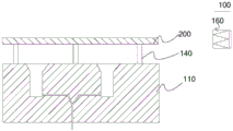
Referring to fig. 3, a first aspect of the present invention relates to a substrate carrier 100, the substrate carrier 100 comprising a body 110 and at least one first static eliminator 120. The body 110 includes a first surface 111 and a second surface 112 disposed opposite to each other, wherein the first surface 111 is used for supporting the substrate 200, and the first surface 111 is further provided with at least one ion channel 113. Each first static eliminator 120 corresponds to at least one ion channel 113, and the first static eliminator 120 is connected to its corresponding ion channel 113 to supply static eliminating ions into the ion channel 113.
That is, as shown in fig. 3, the substrate stage 100 may include a plurality of first static eliminators 120 and a plurality of ion channels 113 disposed on the first surface 111, and each of the first static eliminators 120 may correspond to one of the ion channels 113. Of course, each of the first static eliminator 120 may also correspond to two or more ion channels 113, and so on, according to actual needs.
In this way, when the substrate 200 is peeled off from the substrate stage 100, the first static eliminator 120 can be controlled to be in an open state so that the static eliminating ions can be supplied into the ion channel 113, and the static eliminating ions located in the ion channel 113 can move to the surface of the substrate 200 in contact with the substrate stage 100, that is, the lower surface of the substrate 200 in fig. 3. In this way, static electricity generated between the substrate 200 and the substrate stage 100 can be neutralized by the static electricity eliminating ions, that is, the static electricity eliminating ions are positive ions and negative ions, and neutralize positive and negative charges on the substrate 200 and the substrate stage 100, so that there is no electrostatic adsorption between the substrate 200 and the substrate stage 100, and the substrate 200 can be easily removed from the substrate stage 100.
In the substrate stage 100 having the structure of this embodiment, the ion channel 113 and the first static eliminator 120 corresponding to the ion channel are provided on the first surface 111 of the carrier substrate 200, so that static electricity generated on the surface of the substrate 200 in contact with the substrate stage 100 can be eliminated, electrostatic attraction between the substrate 200 and the substrate stage 100 can be eliminated, and the substrate 200 and the substrate stage 100 can be easily peeled off. Therefore, in the process of peeling the substrate 200 from the substrate carrier 100, the substrate carrier 100 with the structure of the embodiment can effectively protect the substrate 200, effectively avoid the risk of fragments when the substrate 200 is peeled, improve the manufacturing yield of the substrate 200, and reduce the manufacturing cost.
It should be noted that the specific structure of the first static eliminator 120 is not limited, and it is sufficient to supply static eliminating ions into the ion channel 113. For example, the first static eliminator 120 may independently generate and output static eliminating ions, such as an ion flow type static eliminator, which may output positive ions or negative ions to neutralize static electricity generated between the substrate 200 and the substrate stage 100. For another example, the first electrostatic eliminator 120 may also emit some kind of electric laser, which may ionize a gas to generate positive ions or negative ions to neutralize the static electricity generated between the substrate 200 and the substrate carrier 100. Of course, the first static eliminator 120 may be other kinds of static eliminators according to the principle of eliminating static electricity, and is not limited herein.
Preferably, as shown in fig. 3, the substrate stage 100 includes a plurality of first static eliminators 120, and the first static eliminators 120 are disposed in one-to-one correspondence with the ion channels 113. That is, as shown in fig. 3, one first static eliminator 120 is provided at each ion channel 113.
In this way, when the substrate 200 is peeled off from the substrate stage 100, each first static eliminator 120 can be controlled to be in an open state so that the static eliminating ions can be transported into each ion channel 113 corresponding thereto, and the static eliminating ions located in each ion channel 113 can move to the surface of the substrate 200 in contact with the substrate stage 100, that is, the lower surface of the substrate 200 in fig. 1. In this way, static electricity generated between the substrate 200 and the substrate stage 100 can be neutralized by the static electricity eliminating ions, that is, the static electricity eliminating ions are positive ions and negative ions, and neutralize positive and negative charges on the substrate 200 and the substrate stage 100, so that there is no electrostatic adsorption between the substrate 200 and the substrate stage 100, and the substrate 200 can be easily removed from the substrate stage 100.
The substrate stage 100 having the structure of this embodiment is provided with the plurality of first static eliminators 120, and each first static eliminators 120 corresponds to one ion channel 113, so that the rate of eliminating static electricity between the substrate 200 and the substrate stage 100 can be increased, the time for peeling the substrate 200 from the substrate stage 100 can be shortened, the production efficiency can be improved, and the manufacturing cost can be reduced.
Preferably, as a first specific installation manner of the first static eliminator 120 described above, as shown in fig. 3, the first static eliminator 120 may be installed in the ion channel 113 corresponding thereto. That is, as shown in fig. 3, the ion channel 113 may be a pore structure that is recessed from the first surface 111 toward the second surface 112, but does not penetrate the second surface 112. That is, the ion channel 113 is a blind hole structure. Thus, the first static eliminator 120 can be installed inside the ion channel 113.
In the substrate stage 100 of the present embodiment, the first static eliminator 120 is directly installed in the corresponding ion channel 113, and the installation manner is simple, for example, the first static eliminator 120 can be stably fixed in the ion channel 113 by interference fit or transition fit between the first static eliminator 120 and the ion channel 113.
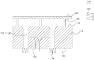
Preferably, as a second specific installation manner of the first static eliminator 120, as shown in fig. 4, the ion channel 113 may completely penetrate the first surface 111 and the second surface 112. That is, the ion channel 113 is a kind of through-hole structure. Thus, the first static eliminator 120 may be installed at the second surface 112, that is, the first static eliminator 120 is located at an end position of the ion channel 113 at the second surface 112, so that the first static eliminator 120 is connected to the ion channel 113 at the position.
Unlike the first embodiment of the first static eliminator 120, in the second embodiment, it is not necessary to consider the size of each ion channel 113 provided, as long as the static eliminating ions can be transmitted. Therefore, in the second mounting method of the first static eliminator 120, the structural stability of the substrate stage 100 can be effectively improved, and the reliability of the carrier substrate 200 can be improved.
Preferably, in order to facilitate the separation of the substrate 200 from the substrate carrier 100, as shown in fig. 3 and 4, the first surface 111 is further provided with at least one air inlet channel 114. The substrate carrier 100 further comprises at least one gas inlet tube 130 and at least one support member 140. Each intake pipe 130 corresponds to at least one intake passage 114, and each intake pipe 130 communicates with its corresponding intake passage 114 to supply gas into the passage 114. The supporting members 140 are telescopically disposed on the first surface 111 to lift the substrate 200 or put the substrate 200 down under the driving of gas.
That is, when it is necessary to peel off the substrate 200 from the substrate stage 100, first, static electricity generated between the substrate 200 and the substrate stage 100 is eliminated by the first static eliminator 120. Then, the gas inlet pipe 130 is used to provide gas (for example, air or nitrogen gas) into the gas inlet channel 114, and since the substrate 200, the supporting member 140 and the first surface 111 are in a sealed environment, the supporting member 140 can be pushed out towards the substrate 200 under the driving of the gas pressure, so that the substrate 200 can be pushed up, and the substrate 200 can be further peeled off from the substrate carrier 100.
It should be understood that other lifting mechanisms may be used in addition to the above-described manner of lifting the substrate 200, for example, a lifting shaft may be disposed in the substrate carrier 100, one end of the lifting shaft is connected to the substrate 200, and the other end is connected to a power source (e.g., a linear module), etc.
Preferably, as shown in fig. 3 and 4, the ion channel 113 is multiplexed into the gas inlet channel 114. That is, as shown in fig. 3 and 4, the ion channel 113 serves as a channel for both static electricity eliminating ions and gas. Therefore, the structure of the substrate stage 100 can be further simplified, the structural stability of the substrate stage 100 can be effectively improved, and the reliability of the carrier substrate 200 can be improved.
In addition, when the ion channel 113 penetrates the first surface 111 and the second surface 112, and it is multiplexed as the gas inlet channel 114, the first static eliminator 120 should be hermetically connected to the ion channel 113 corresponding thereto. In this way, the sealing performance between the substrate 200 and the entire substrate stage 100 can be improved, and thus the time required for peeling the substrate 200 and the substrate stage 100 can be shortened, the production efficiency can be improved, and the production cost can be reduced.
Preferably, the substrate stage 100 further includes a second static eliminator 150, and the second static eliminator 150 is located outside the first surface 111 at a predetermined distance from the first surface 111.
That is, as shown in fig. 4, the second static eliminator 150 may be located above one side of the first surface 111 (e.g., at a right upper position of the first surface 111 in fig. 4). Thus, the second static eliminator 150 can eliminate static electricity on the upper surface of the substrate 200. Therefore, the substrate carrier 100 of the present embodiment can effectively remove the static electricity on the substrate 200, so that the substrate 200 is effectively protected during the peeling process between the substrate 200 and the substrate carrier 100, the risk of fragments occurring during the peeling process of the substrate 200 is effectively avoided, the manufacturing yield of the substrate 200 is improved, and the manufacturing cost is reduced.
In addition, the second static eliminator 150 may be provided outside the first surface 111, and static elimination or the like may be performed by an ion bar at the exit of the apparatus when the substrate 200 is carried out of the apparatus.
Preferably, as a specific structure of the above-described first static eliminator 120, the first static eliminator 120 may include an ion flow type static eliminator and/or a radiation type static eliminator.
The second static eliminator 150 may be an ion flow type static eliminator and/or a radiation type static eliminator.
The ion flow type static eliminator can generate positive and negative ions, so that positive and negative charges between the substrate 200 and the substrate stage 100 can be neutralized.
The radiation type static eliminator may be, for example, an X-ray static eliminator, and it is possible to neutralize positive and negative charges between the substrate 200 and the substrate stage 100 by ionizing air by X-rays generated thereby to generate positive and negative ions.
In a second aspect of the present invention, an exposure machine (not shown) is provided. The exposure apparatus includes the substrate stage 100 described above.
Therefore, in the exposure apparatus having the structure of the substrate stage 100 described above, the substrate stage 100 can eliminate the static electricity generated on the surface of the substrate 200 in contact with the substrate stage 100 by the action of the ion channel 113 and the first static eliminator 120 corresponding to the ion channel provided on the first surface 111 of the carrier substrate 200, so that the electrostatic attraction between the substrate 200 and the substrate stage 100 can be eliminated, and the substrate 200 and the substrate stage 100 can be easily peeled off. Therefore, in the process of peeling the substrate 200 from the substrate carrier 100, the exposure machine with the structure of the embodiment can effectively protect the substrate 200, effectively avoid the risk of fragments when the substrate 200 is peeled, improve the manufacturing yield of the substrate 200, and reduce the manufacturing cost.
It will be understood that the above embodiments are merely exemplary embodiments taken to illustrate the principles of the present invention, which is not limited thereto. It will be apparent to those skilled in the art that various modifications and improvements can be made without departing from the spirit and substance of the invention, and these modifications and improvements are also considered to be within the scope of the invention.