CN108140616B - Semiconductor device with a plurality of transistors - Google Patents
Semiconductor device with a plurality of transistors Download PDFInfo
- Publication number
- CN108140616B CN108140616B CN201580083834.6A CN201580083834A CN108140616B CN 108140616 B CN108140616 B CN 108140616B CN 201580083834 A CN201580083834 A CN 201580083834A CN 108140616 B CN108140616 B CN 108140616B
- Authority
- CN
- China
- Prior art keywords
- capacitor
- wiring
- terminal
- semiconductor device
- semiconductor chip
- Prior art date
- Legal status (The legal status is an assumption and is not a legal conclusion. Google has not performed a legal analysis and makes no representation as to the accuracy of the status listed.)
- Active
Links
Images


Classifications
-
- H—ELECTRICITY
- H01—ELECTRIC ELEMENTS
- H01L—SEMICONDUCTOR DEVICES NOT COVERED BY CLASS H10
- H01L23/00—Details of semiconductor or other solid state devices
- H01L23/58—Structural electrical arrangements for semiconductor devices not otherwise provided for, e.g. in combination with batteries
- H01L23/64—Impedance arrangements
- H01L23/642—Capacitive arrangements
-
- H—ELECTRICITY
- H01—ELECTRIC ELEMENTS
- H01L—SEMICONDUCTOR DEVICES NOT COVERED BY CLASS H10
- H01L25/00—Assemblies consisting of a plurality of individual semiconductor or other solid state devices ; Multistep manufacturing processes thereof
- H01L25/03—Assemblies consisting of a plurality of individual semiconductor or other solid state devices ; Multistep manufacturing processes thereof all the devices being of a type provided for in the same subgroup of groups H01L27/00 - H01L33/00, or in a single subclass of H10K, H10N, e.g. assemblies of rectifier diodes
- H01L25/04—Assemblies consisting of a plurality of individual semiconductor or other solid state devices ; Multistep manufacturing processes thereof all the devices being of a type provided for in the same subgroup of groups H01L27/00 - H01L33/00, or in a single subclass of H10K, H10N, e.g. assemblies of rectifier diodes the devices not having separate containers
- H01L25/065—Assemblies consisting of a plurality of individual semiconductor or other solid state devices ; Multistep manufacturing processes thereof all the devices being of a type provided for in the same subgroup of groups H01L27/00 - H01L33/00, or in a single subclass of H10K, H10N, e.g. assemblies of rectifier diodes the devices not having separate containers the devices being of a type provided for in group H01L27/00
- H01L25/0655—Assemblies consisting of a plurality of individual semiconductor or other solid state devices ; Multistep manufacturing processes thereof all the devices being of a type provided for in the same subgroup of groups H01L27/00 - H01L33/00, or in a single subclass of H10K, H10N, e.g. assemblies of rectifier diodes the devices not having separate containers the devices being of a type provided for in group H01L27/00 the devices being arranged next to each other
-
- H—ELECTRICITY
- H01—ELECTRIC ELEMENTS
- H01L—SEMICONDUCTOR DEVICES NOT COVERED BY CLASS H10
- H01L23/00—Details of semiconductor or other solid state devices
- H01L23/48—Arrangements for conducting electric current to or from the solid state body in operation, e.g. leads, terminal arrangements ; Selection of materials therefor
- H01L23/488—Arrangements for conducting electric current to or from the solid state body in operation, e.g. leads, terminal arrangements ; Selection of materials therefor consisting of soldered or bonded constructions
- H01L23/498—Leads, i.e. metallisations or lead-frames on insulating substrates, e.g. chip carriers
- H01L23/49822—Multilayer substrates
-
- H—ELECTRICITY
- H01—ELECTRIC ELEMENTS
- H01G—CAPACITORS; CAPACITORS, RECTIFIERS, DETECTORS, SWITCHING DEVICES OR LIGHT-SENSITIVE DEVICES, OF THE ELECTROLYTIC TYPE
- H01G2/00—Details of capacitors not covered by a single one of groups H01G4/00-H01G11/00
- H01G2/02—Mountings
- H01G2/06—Mountings specially adapted for mounting on a printed-circuit support
- H01G2/065—Mountings specially adapted for mounting on a printed-circuit support for surface mounting, e.g. chip capacitors
-
- H—ELECTRICITY
- H01—ELECTRIC ELEMENTS
- H01G—CAPACITORS; CAPACITORS, RECTIFIERS, DETECTORS, SWITCHING DEVICES OR LIGHT-SENSITIVE DEVICES, OF THE ELECTROLYTIC TYPE
- H01G4/00—Fixed capacitors; Processes of their manufacture
- H01G4/38—Multiple capacitors, i.e. structural combinations of fixed capacitors
-
- H—ELECTRICITY
- H01—ELECTRIC ELEMENTS
- H01G—CAPACITORS; CAPACITORS, RECTIFIERS, DETECTORS, SWITCHING DEVICES OR LIGHT-SENSITIVE DEVICES, OF THE ELECTROLYTIC TYPE
- H01G4/00—Fixed capacitors; Processes of their manufacture
- H01G4/40—Structural combinations of fixed capacitors with other electric elements, the structure mainly consisting of a capacitor, e.g. RC combinations
-
- H—ELECTRICITY
- H01—ELECTRIC ELEMENTS
- H01L—SEMICONDUCTOR DEVICES NOT COVERED BY CLASS H10
- H01L21/00—Processes or apparatus adapted for the manufacture or treatment of semiconductor or solid state devices or of parts thereof
- H01L21/02—Manufacture or treatment of semiconductor devices or of parts thereof
- H01L21/04—Manufacture or treatment of semiconductor devices or of parts thereof the devices having at least one potential-jump barrier or surface barrier, e.g. PN junction, depletion layer or carrier concentration layer
- H01L21/48—Manufacture or treatment of parts, e.g. containers, prior to assembly of the devices, using processes not provided for in a single one of the subgroups H01L21/06 - H01L21/326
- H01L21/4814—Conductive parts
- H01L21/4846—Leads on or in insulating or insulated substrates, e.g. metallisation
- H01L21/4853—Connection or disconnection of other leads to or from a metallisation, e.g. pins, wires, bumps
-
- H—ELECTRICITY
- H01—ELECTRIC ELEMENTS
- H01L—SEMICONDUCTOR DEVICES NOT COVERED BY CLASS H10
- H01L21/00—Processes or apparatus adapted for the manufacture or treatment of semiconductor or solid state devices or of parts thereof
- H01L21/02—Manufacture or treatment of semiconductor devices or of parts thereof
- H01L21/04—Manufacture or treatment of semiconductor devices or of parts thereof the devices having at least one potential-jump barrier or surface barrier, e.g. PN junction, depletion layer or carrier concentration layer
- H01L21/48—Manufacture or treatment of parts, e.g. containers, prior to assembly of the devices, using processes not provided for in a single one of the subgroups H01L21/06 - H01L21/326
- H01L21/4814—Conductive parts
- H01L21/4846—Leads on or in insulating or insulated substrates, e.g. metallisation
- H01L21/4857—Multilayer substrates
-
- H—ELECTRICITY
- H01—ELECTRIC ELEMENTS
- H01L—SEMICONDUCTOR DEVICES NOT COVERED BY CLASS H10
- H01L21/00—Processes or apparatus adapted for the manufacture or treatment of semiconductor or solid state devices or of parts thereof
- H01L21/02—Manufacture or treatment of semiconductor devices or of parts thereof
- H01L21/04—Manufacture or treatment of semiconductor devices or of parts thereof the devices having at least one potential-jump barrier or surface barrier, e.g. PN junction, depletion layer or carrier concentration layer
- H01L21/48—Manufacture or treatment of parts, e.g. containers, prior to assembly of the devices, using processes not provided for in a single one of the subgroups H01L21/06 - H01L21/326
- H01L21/4814—Conductive parts
- H01L21/4871—Bases, plates or heatsinks
-
- H—ELECTRICITY
- H01—ELECTRIC ELEMENTS
- H01L—SEMICONDUCTOR DEVICES NOT COVERED BY CLASS H10
- H01L22/00—Testing or measuring during manufacture or treatment; Reliability measurements, i.e. testing of parts without further processing to modify the parts as such; Structural arrangements therefor
- H01L22/10—Measuring as part of the manufacturing process
- H01L22/12—Measuring as part of the manufacturing process for structural parameters, e.g. thickness, line width, refractive index, temperature, warp, bond strength, defects, optical inspection, electrical measurement of structural dimensions, metallurgic measurement of diffusions
-
- H—ELECTRICITY
- H01—ELECTRIC ELEMENTS
- H01L—SEMICONDUCTOR DEVICES NOT COVERED BY CLASS H10
- H01L23/00—Details of semiconductor or other solid state devices
- H01L23/12—Mountings, e.g. non-detachable insulating substrates
-
- H—ELECTRICITY
- H01—ELECTRIC ELEMENTS
- H01L—SEMICONDUCTOR DEVICES NOT COVERED BY CLASS H10
- H01L23/00—Details of semiconductor or other solid state devices
- H01L23/16—Fillings or auxiliary members in containers or encapsulations, e.g. centering rings
-
- H—ELECTRICITY
- H01—ELECTRIC ELEMENTS
- H01L—SEMICONDUCTOR DEVICES NOT COVERED BY CLASS H10
- H01L23/00—Details of semiconductor or other solid state devices
- H01L23/34—Arrangements for cooling, heating, ventilating or temperature compensation ; Temperature sensing arrangements
- H01L23/36—Selection of materials, or shaping, to facilitate cooling or heating, e.g. heatsinks
- H01L23/367—Cooling facilitated by shape of device
- H01L23/3675—Cooling facilitated by shape of device characterised by the shape of the housing
-
- H—ELECTRICITY
- H01—ELECTRIC ELEMENTS
- H01L—SEMICONDUCTOR DEVICES NOT COVERED BY CLASS H10
- H01L23/00—Details of semiconductor or other solid state devices
- H01L23/48—Arrangements for conducting electric current to or from the solid state body in operation, e.g. leads, terminal arrangements ; Selection of materials therefor
- H01L23/488—Arrangements for conducting electric current to or from the solid state body in operation, e.g. leads, terminal arrangements ; Selection of materials therefor consisting of soldered or bonded constructions
- H01L23/498—Leads, i.e. metallisations or lead-frames on insulating substrates, e.g. chip carriers
- H01L23/49838—Geometry or layout
-
- H—ELECTRICITY
- H01—ELECTRIC ELEMENTS
- H01L—SEMICONDUCTOR DEVICES NOT COVERED BY CLASS H10
- H01L23/00—Details of semiconductor or other solid state devices
- H01L23/48—Arrangements for conducting electric current to or from the solid state body in operation, e.g. leads, terminal arrangements ; Selection of materials therefor
- H01L23/50—Arrangements for conducting electric current to or from the solid state body in operation, e.g. leads, terminal arrangements ; Selection of materials therefor for integrated circuit devices, e.g. power bus, number of leads
-
- H—ELECTRICITY
- H01—ELECTRIC ELEMENTS
- H01L—SEMICONDUCTOR DEVICES NOT COVERED BY CLASS H10
- H01L24/00—Arrangements for connecting or disconnecting semiconductor or solid-state bodies; Methods or apparatus related thereto
- H01L24/01—Means for bonding being attached to, or being formed on, the surface to be connected, e.g. chip-to-package, die-attach, "first-level" interconnects; Manufacturing methods related thereto
- H01L24/10—Bump connectors ; Manufacturing methods related thereto
- H01L24/15—Structure, shape, material or disposition of the bump connectors after the connecting process
- H01L24/16—Structure, shape, material or disposition of the bump connectors after the connecting process of an individual bump connector
-
- H—ELECTRICITY
- H01—ELECTRIC ELEMENTS
- H01L—SEMICONDUCTOR DEVICES NOT COVERED BY CLASS H10
- H01L25/00—Assemblies consisting of a plurality of individual semiconductor or other solid state devices ; Multistep manufacturing processes thereof
-
- H—ELECTRICITY
- H05—ELECTRIC TECHNIQUES NOT OTHERWISE PROVIDED FOR
- H05K—PRINTED CIRCUITS; CASINGS OR CONSTRUCTIONAL DETAILS OF ELECTRIC APPARATUS; MANUFACTURE OF ASSEMBLAGES OF ELECTRICAL COMPONENTS
- H05K1/00—Printed circuits
- H05K1/02—Details
- H05K1/0213—Electrical arrangements not otherwise provided for
- H05K1/0216—Reduction of cross-talk, noise or electromagnetic interference
- H05K1/023—Reduction of cross-talk, noise or electromagnetic interference using auxiliary mounted passive components or auxiliary substances
- H05K1/0231—Capacitors or dielectric substances
-
- H—ELECTRICITY
- H05—ELECTRIC TECHNIQUES NOT OTHERWISE PROVIDED FOR
- H05K—PRINTED CIRCUITS; CASINGS OR CONSTRUCTIONAL DETAILS OF ELECTRIC APPARATUS; MANUFACTURE OF ASSEMBLAGES OF ELECTRICAL COMPONENTS
- H05K1/00—Printed circuits
- H05K1/18—Printed circuits structurally associated with non-printed electric components
- H05K1/182—Printed circuits structurally associated with non-printed electric components associated with components mounted in the printed circuit board, e.g. insert mounted components [IMC]
- H05K1/185—Components encapsulated in the insulating substrate of the printed circuit or incorporated in internal layers of a multilayer circuit
-
- H—ELECTRICITY
- H05—ELECTRIC TECHNIQUES NOT OTHERWISE PROVIDED FOR
- H05K—PRINTED CIRCUITS; CASINGS OR CONSTRUCTIONAL DETAILS OF ELECTRIC APPARATUS; MANUFACTURE OF ASSEMBLAGES OF ELECTRICAL COMPONENTS
- H05K3/00—Apparatus or processes for manufacturing printed circuits
- H05K3/46—Manufacturing multilayer circuits
-
- G—PHYSICS
- G01—MEASURING; TESTING
- G01R—MEASURING ELECTRIC VARIABLES; MEASURING MAGNETIC VARIABLES
- G01R31/00—Arrangements for testing electric properties; Arrangements for locating electric faults; Arrangements for electrical testing characterised by what is being tested not provided for elsewhere
- G01R31/28—Testing of electronic circuits, e.g. by signal tracer
- G01R31/2832—Specific tests of electronic circuits not provided for elsewhere
- G01R31/2836—Fault-finding or characterising
-
- H—ELECTRICITY
- H01—ELECTRIC ELEMENTS
- H01G—CAPACITORS; CAPACITORS, RECTIFIERS, DETECTORS, SWITCHING DEVICES OR LIGHT-SENSITIVE DEVICES, OF THE ELECTROLYTIC TYPE
- H01G2/00—Details of capacitors not covered by a single one of groups H01G4/00-H01G11/00
- H01G2/02—Mountings
- H01G2/06—Mountings specially adapted for mounting on a printed-circuit support
-
- H—ELECTRICITY
- H01—ELECTRIC ELEMENTS
- H01L—SEMICONDUCTOR DEVICES NOT COVERED BY CLASS H10
- H01L2224/00—Indexing scheme for arrangements for connecting or disconnecting semiconductor or solid-state bodies and methods related thereto as covered by H01L24/00
- H01L2224/01—Means for bonding being attached to, or being formed on, the surface to be connected, e.g. chip-to-package, die-attach, "first-level" interconnects; Manufacturing methods related thereto
- H01L2224/10—Bump connectors; Manufacturing methods related thereto
- H01L2224/15—Structure, shape, material or disposition of the bump connectors after the connecting process
- H01L2224/16—Structure, shape, material or disposition of the bump connectors after the connecting process of an individual bump connector
- H01L2224/161—Disposition
- H01L2224/16151—Disposition the bump connector connecting between a semiconductor or solid-state body and an item not being a semiconductor or solid-state body, e.g. chip-to-substrate, chip-to-passive
- H01L2224/16221—Disposition the bump connector connecting between a semiconductor or solid-state body and an item not being a semiconductor or solid-state body, e.g. chip-to-substrate, chip-to-passive the body and the item being stacked
- H01L2224/16225—Disposition the bump connector connecting between a semiconductor or solid-state body and an item not being a semiconductor or solid-state body, e.g. chip-to-substrate, chip-to-passive the body and the item being stacked the item being non-metallic, e.g. insulating substrate with or without metallisation
- H01L2224/16227—Disposition the bump connector connecting between a semiconductor or solid-state body and an item not being a semiconductor or solid-state body, e.g. chip-to-substrate, chip-to-passive the body and the item being stacked the item being non-metallic, e.g. insulating substrate with or without metallisation the bump connector connecting to a bond pad of the item
-
- H—ELECTRICITY
- H01—ELECTRIC ELEMENTS
- H01L—SEMICONDUCTOR DEVICES NOT COVERED BY CLASS H10
- H01L2224/00—Indexing scheme for arrangements for connecting or disconnecting semiconductor or solid-state bodies and methods related thereto as covered by H01L24/00
- H01L2224/01—Means for bonding being attached to, or being formed on, the surface to be connected, e.g. chip-to-package, die-attach, "first-level" interconnects; Manufacturing methods related thereto
- H01L2224/26—Layer connectors, e.g. plate connectors, solder or adhesive layers; Manufacturing methods related thereto
- H01L2224/31—Structure, shape, material or disposition of the layer connectors after the connecting process
- H01L2224/32—Structure, shape, material or disposition of the layer connectors after the connecting process of an individual layer connector
- H01L2224/321—Disposition
- H01L2224/32151—Disposition the layer connector connecting between a semiconductor or solid-state body and an item not being a semiconductor or solid-state body, e.g. chip-to-substrate, chip-to-passive
- H01L2224/32221—Disposition the layer connector connecting between a semiconductor or solid-state body and an item not being a semiconductor or solid-state body, e.g. chip-to-substrate, chip-to-passive the body and the item being stacked
- H01L2224/32225—Disposition the layer connector connecting between a semiconductor or solid-state body and an item not being a semiconductor or solid-state body, e.g. chip-to-substrate, chip-to-passive the body and the item being stacked the item being non-metallic, e.g. insulating substrate with or without metallisation
-
- H—ELECTRICITY
- H01—ELECTRIC ELEMENTS
- H01L—SEMICONDUCTOR DEVICES NOT COVERED BY CLASS H10
- H01L2224/00—Indexing scheme for arrangements for connecting or disconnecting semiconductor or solid-state bodies and methods related thereto as covered by H01L24/00
- H01L2224/73—Means for bonding being of different types provided for in two or more of groups H01L2224/10, H01L2224/18, H01L2224/26, H01L2224/34, H01L2224/42, H01L2224/50, H01L2224/63, H01L2224/71
- H01L2224/732—Location after the connecting process
- H01L2224/73201—Location after the connecting process on the same surface
- H01L2224/73203—Bump and layer connectors
- H01L2224/73204—Bump and layer connectors the bump connector being embedded into the layer connector
-
- H—ELECTRICITY
- H01—ELECTRIC ELEMENTS
- H01L—SEMICONDUCTOR DEVICES NOT COVERED BY CLASS H10
- H01L2224/00—Indexing scheme for arrangements for connecting or disconnecting semiconductor or solid-state bodies and methods related thereto as covered by H01L24/00
- H01L2224/73—Means for bonding being of different types provided for in two or more of groups H01L2224/10, H01L2224/18, H01L2224/26, H01L2224/34, H01L2224/42, H01L2224/50, H01L2224/63, H01L2224/71
- H01L2224/732—Location after the connecting process
- H01L2224/73251—Location after the connecting process on different surfaces
- H01L2224/73253—Bump and layer connectors
-
- H—ELECTRICITY
- H01—ELECTRIC ELEMENTS
- H01L—SEMICONDUCTOR DEVICES NOT COVERED BY CLASS H10
- H01L2924/00—Indexing scheme for arrangements or methods for connecting or disconnecting semiconductor or solid-state bodies as covered by H01L24/00
- H01L2924/15—Details of package parts other than the semiconductor or other solid state devices to be connected
- H01L2924/151—Die mounting substrate
- H01L2924/153—Connection portion
- H01L2924/1531—Connection portion the connection portion being formed only on the surface of the substrate opposite to the die mounting surface
- H01L2924/15311—Connection portion the connection portion being formed only on the surface of the substrate opposite to the die mounting surface being a ball array, e.g. BGA
-
- H—ELECTRICITY
- H01—ELECTRIC ELEMENTS
- H01L—SEMICONDUCTOR DEVICES NOT COVERED BY CLASS H10
- H01L2924/00—Indexing scheme for arrangements or methods for connecting or disconnecting semiconductor or solid-state bodies as covered by H01L24/00
- H01L2924/15—Details of package parts other than the semiconductor or other solid state devices to be connected
- H01L2924/161—Cap
- H01L2924/1615—Shape
- H01L2924/16195—Flat cap [not enclosing an internal cavity]
-
- H—ELECTRICITY
- H01—ELECTRIC ELEMENTS
- H01L—SEMICONDUCTOR DEVICES NOT COVERED BY CLASS H10
- H01L2924/00—Indexing scheme for arrangements or methods for connecting or disconnecting semiconductor or solid-state bodies as covered by H01L24/00
- H01L2924/19—Details of hybrid assemblies other than the semiconductor or other solid state devices to be connected
- H01L2924/1901—Structure
- H01L2924/1904—Component type
- H01L2924/19041—Component type being a capacitor
-
- H—ELECTRICITY
- H01—ELECTRIC ELEMENTS
- H01L—SEMICONDUCTOR DEVICES NOT COVERED BY CLASS H10
- H01L2924/00—Indexing scheme for arrangements or methods for connecting or disconnecting semiconductor or solid-state bodies as covered by H01L24/00
- H01L2924/19—Details of hybrid assemblies other than the semiconductor or other solid state devices to be connected
- H01L2924/191—Disposition
- H01L2924/19101—Disposition of discrete passive components
- H01L2924/19102—Disposition of discrete passive components in a stacked assembly with the semiconductor or solid state device
- H01L2924/19103—Disposition of discrete passive components in a stacked assembly with the semiconductor or solid state device interposed between the semiconductor or solid-state device and the die mounting substrate, i.e. chip-on-passive
-
- H—ELECTRICITY
- H01—ELECTRIC ELEMENTS
- H01L—SEMICONDUCTOR DEVICES NOT COVERED BY CLASS H10
- H01L2924/00—Indexing scheme for arrangements or methods for connecting or disconnecting semiconductor or solid-state bodies as covered by H01L24/00
- H01L2924/19—Details of hybrid assemblies other than the semiconductor or other solid state devices to be connected
- H01L2924/191—Disposition
- H01L2924/19101—Disposition of discrete passive components
- H01L2924/19105—Disposition of discrete passive components in a side-by-side arrangement on a common die mounting substrate
-
- H—ELECTRICITY
- H01—ELECTRIC ELEMENTS
- H01L—SEMICONDUCTOR DEVICES NOT COVERED BY CLASS H10
- H01L2924/00—Indexing scheme for arrangements or methods for connecting or disconnecting semiconductor or solid-state bodies as covered by H01L24/00
- H01L2924/30—Technical effects
- H01L2924/35—Mechanical effects
- H01L2924/351—Thermal stress
- H01L2924/3511—Warping
Abstract
The semiconductor device includes: a wiring substrate having a first surface and a second surface opposite to the first surface; a semiconductor chip mounted on the wiring substrate and including a plurality of chip electrodes; a first capacitor which is arranged at a position overlapping with the semiconductor chip in a plan view and is built in the wiring substrate; and a second capacitor arranged between the first capacitor and a peripheral portion of the wiring substrate in a plan view. The second capacitor is inserted in a signal transmission path for inputting or outputting an electric signal to or from the semiconductor chip in a series connection.
Description
Technical Field
The present invention relates to a semiconductor device having a wiring substrate on which, for example, a semiconductor chip and a capacitor are mounted.
Background
Jp 2010-21275 a (patent document 1), jp 2009-38111 a (patent document 2), jp 2012-89590 a (patent document 3), and international publication No. 2006/001087 (patent document 4) describe semiconductor devices in which chip components such as a semiconductor chip and a capacitor are mounted on a wiring board.
Documents of the prior art
Patent document
Patent document 1: japanese laid-open patent publication No. 2010-21275
Patent document 2: japanese laid-open patent publication No. 2009-38111
Patent document 3: japanese laid-open patent publication No. 2012-89590
Patent document 4: international publication No. 2006/001087
Disclosure of Invention
There is a technique of mounting a plurality of semiconductor devices on a wiring substrate such as a motherboard and connecting a capacitor in series to a signal path that electrically connects the plurality of semiconductor devices to each other. This capacitor is called a DC (Direct Current) blocking capacitor or an AC (alternating Current) coupling capacitor (hereinafter referred to as a DC blocking capacitor) for blocking a DC component contained in an AC signal.
The present inventors have studied a technology of mounting a DC blocking capacitor, which has been conventionally mounted on a wiring board, in a semiconductor device as one part of a design for reducing the size of an electronic device that inputs and outputs signals between a plurality of semiconductor devices as described above.
As a result of the above-described examination, it is found that when only the DC blocking capacitor is incorporated in the semiconductor device, there is a problem in terms of the electrical characteristics and reliability of the semiconductor device depending on the layout of the capacitor.
Other problems and novel features will become apparent from the description and drawings of the present specification.
The semiconductor device of an embodiment includes: a wiring substrate having a first surface and a second surface opposite to the first surface; a semiconductor chip mounted on the wiring substrate and including a plurality of chip electrodes; a first capacitor which is arranged at a position overlapping with the semiconductor chip in a plan view and is built in the wiring substrate; and a second capacitor arranged between the first capacitor and a peripheral portion of the wiring substrate in a plan view. The second capacitor is inserted in a signal transmission path for inputting or outputting an electric signal to or from the semiconductor chip in a series connection.
Effects of the invention
According to the above embodiment, the electrical characteristics and reliability of the semiconductor device can be improved.
Drawings
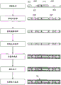
Fig. 1 is an explanatory diagram showing a configuration example of an electronic device including a semiconductor device as an embodiment.
Fig. 2 is an explanatory diagram showing a configuration example of a circuit provided in the electronic device shown in fig. 1.
Fig. 3 is a plan view of a semiconductor device having a DC blocking capacitor built therein among the plurality of semiconductor devices shown in fig. 1.
Fig. 4 is a bottom view of the semiconductor device shown in fig. 3.
Fig. 5 is a plan view showing an internal structure of the semiconductor device on the wiring substrate with the heat sink shown in fig. 3 removed.
Fig. 6 is a sectional view taken along line a-a of fig. 3.
Fig. 7 is a plan view showing one of the plurality of capacitors shown in fig. 5.
Fig. 8 is a sectional view taken along line a-a of fig. 7.
Fig. 9 is an enlarged cross-sectional view of a semiconductor device as a modification to fig. 6.
Fig. 10 is an enlarged cross-sectional view schematically showing an example of a signal transmission path connected to the DC blocking capacitor shown in fig. 5.
Fig. 11 is an enlarged plan view showing an enlarged periphery of a region in which a DC blocking capacitor is incorporated in the semiconductor device according to the modification to fig. 5.
Fig. 12 is an enlarged cross-sectional view of the semiconductor device shown in fig. 11.
Fig. 13 is an enlarged plan view showing an enlarged periphery of a region in which a DC blocking capacitor is incorporated in the semiconductor device according to another modification to fig. 5.
Fig. 14 is an enlarged cross-sectional view of the semiconductor device shown in fig. 13.
Fig. 15 is an enlarged plan view of the wiring layer in which the capacitor is embedded among the plurality of wiring layers shown in fig. 10.
Fig. 16 is an enlarged plan view of a wiring layer on the upper layer of the wiring layer shown in fig. 15.
Fig. 17 is an enlarged plan view of a wiring layer on the upper layer of the wiring layer shown in fig. 16.
Fig. 18 is a main part sectional view showing a relationship between a capacitor constituting the high-speed transmission line shown in fig. 10 and a core insulating layer on which a via wiring is formed.
Fig. 19 is a main part cross-sectional view showing a relationship between a capacitor and a core insulating layer on which a via wiring is formed, which is a semiconductor device according to a modification to fig. 18.
Fig. 20 is a main part cross-sectional view showing a relationship between a capacitor and a core insulating layer on which a via wiring is formed, which is a semiconductor device according to another modification to fig. 18.
Fig. 21 is a main part sectional view showing an example of an embodiment in which via wirings are connected to capacitors built in a wiring substrate.
Fig. 22 is a main part sectional view showing an example of connecting via wirings to a capacitor built in a wiring substrate, which is different from the embodiment of fig. 21.
Fig. 23 is a partial cross-sectional view showing an example of connecting via wirings to capacitors built in a wiring substrate, which is different from the embodiments of fig. 21 and 22.
Fig. 24 is a partial cross-sectional view showing an example of the embodiment of fig. 21 to 23 in which via wirings are connected to capacitors built in a wiring substrate.
Fig. 25 is an explanatory diagram showing an outline of a manufacturing process of a semiconductor device according to an embodiment.
Fig. 26 is an explanatory diagram illustrating an example of a manufacturing process of the wiring substrate prepared in the wiring substrate preparation process shown in fig. 25.
Fig. 27 is an enlarged cross-sectional view schematically showing a state in which the electrodes of the DC blocking capacitor are short-circuited and inspected in the electrical test process shown in fig. 25.
Fig. 28 is a plan view showing an upper surface side of the semiconductor device as a modification to fig. 1.
Fig. 29 is a bottom view of the semiconductor device shown in fig. 28.
Fig. 30 is an enlarged cross-sectional view schematically showing an example of a signal transmission path connected to a DC blocking capacitor included in the semiconductor device as a modification to fig. 10.
Fig. 31 is an enlarged cross-sectional view schematically showing an example of a signal transmission path connected to a DC blocking capacitor included in a semiconductor device as another modification to fig. 10.
Fig. 32 is a plan view showing a positional relationship between a plurality of capacitors and a semiconductor chip in a perspective plane viewed from the upper surface side of a wiring board included in the semiconductor device as a study example with respect to fig. 5.
Fig. 33 is an enlarged cross-sectional view schematically showing an example of a signal transmission path connected to the DC blocking capacitor shown in fig. 32.
Detailed Description
(description of the forms, basic terms, and usage of the present application)
In the present application, the description of the embodiments is divided into a plurality of stages for convenience as necessary, and the embodiments are not separated from each other independently unless otherwise stated explicitly, and each part of a single example, one part is another part, or a partial or whole modification thereof is described before and after the description. In principle, the same portions will not be described repeatedly. It should be noted that each component in the embodiment is not essential unless otherwise specified, theoretically limited in number, or apparent from the context of the text.
Similarly, in the description of the embodiments and the like, even if "X composed of a" or the like is mentioned as a material, a composition or the like, a case where an element other than a is included is not excluded unless it is specifically stated explicitly or clearly understood from the context. For example, the term "component (a)" means "X containing a as a main component" or the like. For example, even if reference is made to "silicon member" or the like, it is not limited to a single silicon, and naturally includes SiGe (silicon germanium) alloy or other multicomponent alloy having silicon as a main component, members containing other additives, and the like. Note that, even if gold plating, a Cu layer, nickel plating, or the like is mentioned, unless otherwise stated, the present invention includes not only a single component but also members each mainly composed of gold, Cu, nickel, or the like.
Further, when a specific numerical value or amount is mentioned, unless otherwise stated explicitly or explicitly, unless otherwise stated theoretically, unless otherwise stated, or unless otherwise stated explicitly or explicitly stated from the context of the text, the numerical value may be a value exceeding the specific numerical value or a value lower than the specific numerical value.
In the drawings of the embodiments, the same or similar parts are denoted by the same or similar reference numerals, and description thereof will not be repeated in principle.
In the drawings, hatching or the like may be omitted in spite of the cross section in the case where the material is complicated or clearly distinguished from the void. In this connection, as is apparent from the description and the like, even in the case of a hole closed on a plane, the outline of the background may be omitted. Further, even if the cross section is not formed, a cross-sectional line or dot pattern is often formed to clearly show the boundary of the non-void or clear region.
(embodiment mode)
< electronic device >
First, a configuration example of an electronic device in which a plurality of semiconductor devices (semiconductor packages) are mounted on a motherboard and electric signals are transmitted between the plurality of semiconductor devices will be described with reference to fig. 1 and 2. Fig. 1 is an explanatory diagram showing a configuration example of an electronic device including the semiconductor device of the present embodiment. Fig. 2 is an explanatory diagram showing a configuration example of a circuit provided in the electronic device shown in fig. 1. Further, in fig. 1, in order to clearly show that the semiconductor device PKG1 is electrically connected to the semiconductor device PKG2, the high-speed transfer path SGP2 shown in fig. 2 is schematically illustrated by a thick line.
An electronic device (electronic apparatus) EDV1 shown in fig. 1 includes a wiring board (motherboard, mounting board) MB1, a semiconductor device PKG1 mounted on the wiring board MB1, and a semiconductor device PKG2 mounted on the wiring board MB 1. The semiconductor device PKG1 and the semiconductor device PKG2 are electrically connected to each other via a signal transmission path SGP formed on the wiring substrate MB 1.
In detail, as shown in fig. 2, the electronic device EDV1 has a plurality of signal transmission paths SGP. In the example shown in fig. 2, the plurality of signal transmission paths SGP include a low-speed transmission path SGP1 that transmits electrical signals at a first transmission speed and a high-speed transmission path SGP2 that transmits electrical signals at a second transmission speed faster than the first transmission speed. In the example shown in fig. 2, the high-speed transmission path SGP2 includes a pair of differential signal transmission paths DSp and DSn through which differential signals are transmitted.
In the present embodiment, an embodiment in which differential signals are transmitted via a pair of differential signal transmission paths DSp and DSn will be described as an example of the high-speed transmission path SGP2, and various modifications of the type of high-speed signals other than the differential signals can be applied. For example, even in the case of a so-called single-ended structure using one signal transmission path SGP, high-speed transmission can be performed by increasing the frequency.
In the example shown in fig. 2, the electrode (electrode pad) TxL for low-speed signal transmission transmitted at, for example, the first transmission speed is formed on the semiconductor chip 11 included in the semiconductor device PKG 1. Further, the semiconductor chip 11 is provided with an electrode (electrode pad) Tx for high-speed signal transmission (specifically, an electrode Txp and an electrode Txn for outputting a pair of differential signals) which is transmitted at a second transmission speed higher than the first transmission speed, for example.
On the other hand, an electrode (electrode pad) RxL for receiving a low-speed signal transmitted at a first transmission speed is formed on the semiconductor chip 12 included in the semiconductor device PKG 2. Further, the semiconductor chip 12 is provided with an electrode (electrode pad) Rx for receiving a high-speed signal (specifically, an electrode Rxp and an electrode Rxn to which a pair of differential signals are input) which is transmitted at a second transmission speed higher than the first transmission speed, for example.
Further, in the low-speed transmission path SGP1 formed by electrically connecting the electrode TxL and the electrode RxL, an electric signal is transmitted at a transmission speed lower than, for example, 3gbps (gigabit per second). In addition, in the high-speed transmission path SGP2 formed by electrically connecting the electrode Tx and the electrode Rx, an electric signal is transmitted at a transmission speed of, for example, about 3Gbps to 100 Gbps.
In the case of transmitting a signal at high speed as in the electronic device EDV1, the capacitor 20D is preferably connected in series to the high-speed transmission path SGP 2. The dc component contained in the ac signal can be blocked (in other words, the dc component can be blocked) by the capacitor 20D inserted into the high-speed transmission path SGP 2. This stabilizes the input/output of high-speed signals. The capacitor 20D inserted in the signal transmission path in series to block the direct current component in the alternating current signal is referred to as a DC (direct current) blocking capacitor, an ac (alternate current) coupling capacitor, or a DC blocking capacitor (hereinafter referred to as a DC blocking capacitor).
The capacitor 20D as a DC blocking capacitor is different from the capacitor 20P for a power supply circuit inserted in the power supply circuit so as to be connected in parallel, such as the capacitor 20P shown in fig. 2. The capacitor 20P shown in fig. 2 is inserted between a reference potential supply path VSP that supplies a reference potential (first potential) VSS to the semiconductor chip 12 and a power supply potential supply path VDP that supplies a power supply potential (second potential) VDD to the semiconductor chip 12. The capacitor 20P can function as a bypass capacitor for bypassing the noise (signal) included in the power supply potential supply path VDP to the reference potential supply path VSP side. The capacitor 20P can function as a decoupling capacitor that reduces the influence of impedance components contained in the power supply potential supply path VDP and the reference potential supply path VSP by reducing the loop (path distance) of the current flowing through the circuit formed in the semiconductor chip 12. Further, capacitor 20P is connected in the vicinity of a circuit that consumes the supplied electric power, and thereby functions as a battery that suppresses a phenomenon in which the drive voltage momentarily drops.
The capacitors 20P for the power supply circuit, which are used as the bypass capacitor, the decoupling capacitor, or the storage battery, are inserted in the power supply circuit in parallel. On the other hand, the capacitor 20D is inserted in the signal transmission path SGP in series. Therefore, as shown in fig. 2, when the high-speed transmission path SGP2 is formed by the differential signal transmission paths DSp and DSn, the capacitor 20D is inserted into each of the differential signal transmission path DSp and the differential signal transmission path DSn.
Further, a state in which the capacitors are connected in series in the wiring path (the signal transmission path or the potential supply path) and a state in which the capacitors are connected in parallel in the wiring path (the signal transmission path or the potential supply path) can be defined in the following manner. That is, the capacitor has two electrodes, and can be defined by the connection destination of the wiring connected to the two electrodes. For example, in
In the example shown in fig. 2, one electrode of the capacitor 20D is connected to the electrode Rx of the semiconductor chip 12 via the first wiring. The other electrode of the capacitor 20D is connected to the contact 3LH via a second wiring different from the first wiring. Then, the contact 3LH and the electrode Rx of the semiconductor chip 12 are electrically connected via the capacitor 20D. In this case, the capacitor 20D can be said to be connected in series in a wiring path that electrically connects the electrode Rx of the semiconductor chip 12 and the contact 3 LH.
Further, one electrode of the capacitor 20P is connected to the electrode Vd of the semiconductor chip 12 and the contact 3LVd via a first wiring. The other electrode of the capacitor 20P is connected to the electrode Vs of the semiconductor chip 12 and the contact 3LVs via a second wiring different from the first wiring. In this case, the capacitor 20P can be said to be connected in parallel between a wiring path for supplying a power supply potential to the semiconductor chip 12 and a wiring path for supplying a reference potential.
Here, as described above, at least one or more capacitors 20D as DC blocking capacitors may be inserted into the high-speed transmission line SGP 2. Therefore, for example, capacitor 20D can be mounted on wiring board MB1 shown in fig. 1. However, the DC blocking capacitor needs to be mounted in accordance with the number of high-speed transmission lines SGP 2. For example, in the case of a high-speed transmission line having a single-ended structure, the same number of capacitors 20D as the number of high-speed transmission lines is required. For example, as shown in fig. 2, in the case of the high-speed transmission path SGP2 for transmitting the differential signal, one (two in total) capacitor 20D is required for each of the high-speed transmission paths SGP of the differential pair.
In this way, when the plurality of capacitors 20D are mounted on the wiring board MB1, the design of the wiring constituting the high-speed transmission path SGP2 becomes complicated among the plurality of wirings formed on the wiring board MB 1. In addition, the design of the wiring becomes complicated, and the electronic device EDV1 is not easily miniaturized.
In the high-speed transmission path SGP2, from the viewpoint of reducing crosstalk noise, the wiring constituting the high-speed transmission path SGP2 is preferably formed on an inner layer of the wiring substrate MB1 shown in fig. 1 (a wiring layer formed on the inner side of the wiring layer on which the terminals for mounting the semiconductor devices PKG1 and PKG2 are formed). However, when the capacitor 20D is mounted on the wiring board MB1, an interlayer conductive path for electrically connecting the stacked wiring layers via a via, a through hole, or the like, not shown, is necessary in order to electrically connect the capacitor 20D and the high-speed transmission path SGP 2. An interlayer conductive path such as a via or a via becomes a cause of impedance discontinuity in the high-speed transmission path SGP 2. Therefore, from the viewpoint of improving the electrical characteristics of the high-speed transmission path SGP2, it is preferable to reduce the number of interlayer conductive paths included in the high-speed transmission path SGP 2.
Therefore, the present inventors have studied a technique of mounting the capacitor 20D as a DC blocking capacitor in the semiconductor device PKG2 as shown in fig. 1. By mounting the capacitor 20D in the semiconductor device PKG2, the layout of the wiring formed on the wiring board MB1 can be simplified. This makes it possible to reduce the size of the wiring board MB 1.
Further, by mounting the capacitor 20D in the semiconductor device PKG2, the number of interlayer conductive paths to be inserted into the high-speed transmission path SGP2 included in the wiring board MB1 can be reduced. This improves the electrical characteristics of the high-speed transmission line SGP 2.
In addition, in this embodiment, as shown in fig. 1, the capacitor 20D is mounted on the semiconductor device PKG2 having a circuit for reception out of the semiconductor device PKG1 having a circuit for transmission and the semiconductor device PKG2 having a circuit for reception. However, as described above, the capacitor 20D may be inserted into one or more high-speed transmission lines SGP 2. Therefore, as a modification to fig. 1, the capacitor 20D may be mounted on the semiconductor device PKG1 having a circuit for transmission, instead of mounting the capacitor 20D on the semiconductor device PKG 2. As another modification to fig. 1, the capacitor 20D may be mounted on both the semiconductor device PKG1 and the semiconductor device PKG 2.
< semiconductor device >
Next, an embodiment in which the DC blocking capacitor 20D is mounted in the semiconductor device PKG2 will be described in detail, taking the semiconductor device PKG2 shown in fig. 1 as an example. Fig. 3 is a plan view of a semiconductor device having a capacitor for DC blocking among the plurality of semiconductor devices shown in fig. 1. Fig. 4 is a bottom view of the semiconductor device shown in fig. 3. Fig. 5 is a plan view showing a positional relationship between the plurality of capacitors and the semiconductor chip in a perspective plane viewed from the upper surface side of the wiring board shown in fig. 3. Fig. 6 is an enlarged sectional view taken along line a-a of fig. 3.
In fig. 3 to 6, the number of terminals is reduced for easy viewing. The number of terminals (terminal 3BF, contact 3LD, solder ball SB) is not limited to the embodiment shown in fig. 6. For example, the present invention can be applied to a semiconductor device in which the number of terminals such as the terminal 3BF, the contact 3LD, and the solder ball SB is about 100 to 10000. In fig. 5, in order to clearly show the positional relationship between the plurality of capacitors and the plane of the semiconductor chip, the outlines of the plurality of capacitors built in the wiring substrate 30 are shown by broken lines. In addition, fig. 5 is a plan view, but hatching lines are attached to the plurality of capacitors 20P in order to easily identify the capacitors 20D and 20P among the plurality of capacitors. Fig. 6 is a cross-sectional view, but hatching is omitted for the respective insulating layers 31 and the underfill resin for easy viewing.
First, a schematic structure of the semiconductor device PKG2 according to this embodiment will be described with reference to fig. 3 to 6. The semiconductor device PKG2 of the present embodiment includes a wiring board 30, a semiconductor chip 12 (see fig. 5) mounted on the wiring board 30, and a plurality of capacitors 20D and 20P built in the wiring board 30.
As shown in fig. 6, the wiring board 30 has an upper surface (surface, main surface, chip mounting surface) 3t on which the semiconductor chip 12 is mounted, a lower surface (surface, main surface, mounting surface) 3b on the opposite side of the upper surface 3t, and a plurality of side surfaces 3s (see fig. 3 to 5) disposed between the upper surface 3t and the lower surface 3b, and forms a quadrangular external shape in plan view as shown in fig. 4 and 5. In the example shown in fig. 4 and 5, the planar dimensions (the dimensions in plan view, the dimensions of the upper surface 3t and the lower surface 3b, and the outer dimensions) of the wiring board 30 form a square or a rectangle, for example, having a side length of about 12mm to 60 mm. The thickness (height) of the wiring board 30, i.e., the distance from the upper surface 3t to the lower surface 3b shown in fig. 6, is, for example, about 0.3mm to 1.3 mm.
The wiring board 30 is an interposer (relay board) for electrically connecting the semiconductor chip 12 mounted on the upper surface 3t side to the wiring board MB1 as a motherboard (mounting board) shown in fig. 1. The wiring board 30 has a plurality of wiring layers (6 layers in the example shown in fig. 6) WL1, WL2, WL3, WL4, WL5, and WL6 that electrically connect the upper surface 3t side as the chip mounting surface and the lower surface 3b side as the mounting surface. Each wiring layer has a conductor pattern such as wiring as a path for supplying an electric signal or power, and is covered with an insulating layer 31 for insulating a plurality of paths. The wiring layers adjacent to each other in the thickness direction are electrically connected to each other by an interlayer conductive path such as via wiring 3V and via wiring 3 TW.
Most of the wiring layer WL1 disposed on the uppermost surface 3T side among the plurality of wiring layers is covered with the insulating layer 31T as a solder resist. Most of the wiring layer WL6 disposed on the lowermost surface 3B side among the plurality of wiring layers is covered with the insulating layer 31B as a solder resist.
The wiring board 30 is formed by laminating a plurality of wiring layers on the upper surface 3Ct and the lower surface 3Cb of an insulating layer (core material, core insulating layer) 31C made of a preform material in which a resin is impregnated into glass fibers, respectively, by a lamination process. The wiring layer WL3 on the upper surface 3Ct side and the wiring layer WL4 on the lower surface 3Cb side of the insulating layer 31C are electrically connected to each other via a plurality of via wirings 3TW embedded in a plurality of through holes (vias) provided to penetrate from one of the upper surface 3Ct and the lower surface 3Cb to the other.
A plurality of terminals (bonding pads, bonding wires, and chip connection terminals) 3BF electrically connected to the semiconductor chip 12 are formed on the upper surface 3t of the wiring substrate 30. In addition, a plurality of contacts 3LD, which are external input/output terminals of the semiconductor device PKG2, are formed on the lower surface 3b of the wiring substrate 30. The plurality of terminals 3BF and the plurality of contacts 3LD are electrically connected to each other via a wiring 3W, a via wiring 3V, and a through-hole wiring 3TW formed on the wiring substrate 30.
In the example shown in fig. 6, the wiring board 30 is a wiring board in which a plurality of wiring layers are stacked on the upper surface 3Ct side and the lower surface 3Cb side of the insulating layer 31C as a core material, respectively. However, as a modification of fig. 6, a so-called coreless substrate may be used which is formed by sequentially laminating an insulating layer 31 and a conductor pattern such as a wire 3W without using an insulating layer 31C made of a hard material such as a prepreg. In the case of using the coreless substrate, the via wiring 3TW is not formed, and the wiring layers are electrically connected via the via wiring 3V. In addition, although the wiring substrate 30 having 6 wiring layers is exemplified in fig. 6, a wiring substrate having 7 or more or 5 or less wiring layers, for example, may be used as a modification.
The wiring layers WL1, WL2, WL3, WL4, and WL6 each have a conductor plane (pattern) 3PL formed so as to surround the periphery of a conductor pattern such as the wiring 3W, the via wiring 3V, the via wiring 3TW, and the contact 3 LD. The conductor plane 3PL is a conductor pattern formed in a region where no conductor pattern such as a wiring or a terminal for signal transmission is formed, and constitutes a part of a supply path of the reference potential or the power supply potential. The conductor plane 3PL is provided separately from conductor patterns such as the wiring 3W, the via wiring 3V, the via wiring 3TW, and the contact 3 LD.
In this way, when the conductor plane 3PL is formed in each wiring layer, it is possible to suppress the diffusion of the electric field and the magnetic field that diffuse from the signal transmission path to the surroundings when transmitting a signal, and to suppress crosstalk noise from other signals. This can improve the noise immunity of the signal transmission path. In particular, when a high-speed transmission path for transmitting a signal at a transmission speed of 3Gbps or more is included as in the present embodiment, it is preferable to improve noise resistance by forming a conductor plane. The conductor plane 3PL may form a return path (return path) of the signal transmission path.
In the example shown in fig. 6, solder balls (solder material, external terminals, electrodes, external electrodes) SB are connected to the plurality of contacts 3LD, respectively. The solder ball SB is a conductive member that electrically connects a plurality of terminals (not shown) on the wiring board MB1 side to a plurality of contacts 3LD when the semiconductor device PKG2 is mounted on the wiring board MB1 shown in fig. 1. The solder ball SB is a solder material composed of a Sn — Pb solder to which lead (Pb) is added or a so-called lead-free solder containing substantially no Pb. Examples of the lead-free solder include tin (Sn) alone, tin-bismuth (Sn-Bi), tin-copper-silver (Sn-Cu-Ag), tin-copper (Sn-Cu), and the like. Here, the lead-free solder is a solder having a lead (Pb) content of 0.1 wt% or less, and the content is determined based on the rohs (restriction of Hazardous substations) instruction.
As shown in fig. 4, a plurality of solder balls SB are arranged in rows and columns (array, matrix). Although not shown in fig. 4, a plurality of contacts 3LD (see fig. 6) to which a plurality of solder balls SB are bonded are also arranged in a row and column (matrix). In this manner, a semiconductor device in which a plurality of external terminals (solder balls SB or contacts 3LD) are arranged in matrix on the mounting surface side of the wiring substrate 30 is referred to as a surface-mount type semiconductor device. The area array type semiconductor device is preferable in that the mounting surface (lower surface 3b) side of the wiring board 30 can be effectively used as an arrangement space for the external terminals, and therefore, an increase in the mounting area of the semiconductor device can be suppressed even if the number of external terminals is increased. That is, a semiconductor device in which the number of external terminals increases with higher functionality and higher integration can be mounted in a space-saving manner.
The semiconductor device PKG2 includes the semiconductor chip 12 mounted on the wiring board 30. As shown in fig. 6, the semiconductor chip 12 has a front surface (main surface, upper surface) 1t, a back surface (main surface, lower surface) 1b opposite to the front surface 1t, and a side surface 1s located between the front surface 1t and the back surface 1b, and forms a rectangular outer shape having a smaller planar area than the wiring substrate 30 in a plan view, as shown in fig. 5. In the example shown in fig. 5, the semiconductor chip 12 is mounted on the upper surface 3t of the wiring board 30 in a state where the four side surfaces 1s are along the four side surfaces 3s of the wiring board 30, respectively.
As shown in fig. 6, a plurality of pads (electrode pads, bonding pads) 1PD are formed on the front surface 1t side of the semiconductor chip 12. The plurality of pads 1PD are exposed from the passivation film protecting the surface 1t of the semiconductor chip 12 on the surface 1t of the semiconductor chip 12. In the present embodiment, a plurality of pads 1PD are arranged in matrix on the surface 1t of the semiconductor chip 12. By arranging the plurality of pads 1PD, which are electrodes of the semiconductor chip 12, in a row and column, the surface 1t of the semiconductor chip 12 can be effectively used as an arrangement space for the electrodes, and therefore, even if the number of electrodes of the semiconductor chip 12 increases, an increase in the planar area can be suppressed, which is preferable. Although not shown in the drawings, the present embodiment can be applied to a semiconductor chip of a type in which a plurality of pads 1PD are formed along each of the edges constituting the peripheral edge of the front surface 1t as a modification.
In the example shown in fig. 6, the semiconductor chip 12 is mounted on the wiring board 30 in a state where the front surface 1t faces the upper surface 3t of the wiring board 30. Such a mounting method is called a face-down mounting method or a flip-chip connection method.
Although not shown, a plurality of semiconductor elements (circuit elements) are formed on the main surface of the semiconductor chip 12 (specifically, a semiconductor element forming region provided on the element forming surface of the semiconductor substrate, which is the base material of the semiconductor chip 12). The plurality of pads 1PD are electrically connected to the plurality of semiconductor elements via wires (not shown) formed in a wiring layer disposed inside the semiconductor chip 12 (specifically, between the front surface 1t and a semiconductor element formation region (not shown)).
The semiconductor chip 12 (specifically, the base material of the semiconductor chip 12) is made of, for example, silicon (Si). An insulating film covering the base material and the wiring of the semiconductor chip 12 is formed on the surface 1t, and a part of each of the plurality of pads 1PD is exposed from the insulating film in an opening formed in the insulating film. Each of the plurality of pads 1PD is made of a metal, and in the present embodiment, is made of, for example, aluminum (Al).
As shown in fig. 6, bump electrodes 1BP are connected to the plurality of pads 1PD, respectively, and the plurality of pads 1PD of the semiconductor chip 12 and the plurality of terminals 3BF of the wiring board 30 are electrically connected to each other via the plurality of bump electrodes 1BP, respectively. The bump electrode (bump electrode) 1BP is a metal member (conductive member) formed to protrude onto the surface 1t of the semiconductor chip 12. The bump electrode 1BP is a so-called solder bump in which a solder material is laminated on the pad 1PD through a base metal film (under bump metal) in the present embodiment. The base metal film may be, for example, a laminated film in which titanium (Ti), copper (Cu), and nickel (Ni) are laminated from the side of the connection surface with the pad 1PD (a gold (Au) film may be further formed on the nickel film). As a solder material constituting the solder bump, a lead-added solder material or a lead-free solder material can be used, similarly to the solder ball SB. When the semiconductor chip 12 is mounted on the wiring board 30, solder bumps are formed in advance on both the plurality of pads 1PD and the plurality of terminals 3BF, and a heating process (reflow process) is performed in a state where the solder bumps are brought into contact with each other, whereby the solder bumps are integrated with each other to form the bump electrodes 1 BP. As a modification to the present embodiment, a pillar bump (pillar electrode) in which a solder film is formed on the tip end surface of a conductive pillar made of copper (Cu) or nickel (Ni) may be used as the protrusion electrode 1 BP.
In the present embodiment, the semiconductor chip 12 has a circuit for inputting and outputting a plurality of signals having different transmission speeds. Although not shown, the semiconductor chip 12 includes a first circuit that inputs and outputs a first signal at a first transmission rate and a second circuit that inputs and outputs a second signal at a second transmission rate higher than the first transmission rate. The second signal is a differential signal transmitted at a transmission rate of, for example, about 3Gbps (gigabit per second) to about 100 Gbps. In the following, in the present embodiment, a transmission path through which the second signal is transmitted will be described as a high-speed transmission path. A transmission path through which the first signal is transmitted at a first transmission speed slower than the second transmission speed will be described as a low-speed transmission path. In addition, the first signal is supplied to the first circuit, and a first driving voltage for driving the first circuit is also supplied to the first circuit. In addition, a second driving voltage for driving the second circuit is supplied to the second circuit in addition to the second signal.
As shown in fig. 6, an underfill resin (insulating resin) 32 is disposed between the semiconductor chip 12 and the wiring board 30. The underfill resin 32 is arranged to fill the space between the surface 1t of the semiconductor chip 12 and the upper surface 3t of the wiring substrate 30. The underfill resin 32 is made of an insulating (non-conductive) material (e.g., a resin material), and is arranged to seal the electrical connection portion between the semiconductor chip 12 and the wiring substrate 30 (the joint portion between the plurality of bump electrodes 1 BP). In this way, by covering the junction between the plurality of bump electrodes 1BP and the plurality of terminals 3BF with the underfill resin 32, stress generated in the electrical connection portion between the semiconductor chip 12 and the wiring substrate 30 can be relaxed. Further, stress generated at the joint portion between the plurality of pads 1PD and the plurality of bump electrodes 1BP of the semiconductor chip 12 can be relaxed. Further, the main surface of the semiconductor chip 12 on which the semiconductor element (circuit element) is formed can be protected.
As shown in fig. 5, the semiconductor device PKG2 includes a plurality of capacitors 20D and 20P mounted on the wiring board 30. The capacitors 20D and 20P are made of, for example, a ceramic material, and in the example of the present embodiment, the semiconductor device PKG2 includes a plurality of capacitors 20D and 20P built in the wiring substrate 30. The above-described "built in the wiring board 30" is defined as follows.
For example, in the example shown in fig. 6, the entire capacitor 20D and the entire capacitor 20P are disposed between the upper surface 3t and the lower surface 3b of the wiring substrate 30. In this case, it can be said that the capacitor 20P and the capacitor 20D are embedded in the wiring substrate 30. On the other hand, the semiconductor chip 12 shown in fig. 6 is not present between the upper surface 3t and the lower surface 3b of the wiring substrate 30. In this case, the semiconductor chip 12 is not built in the wiring board 30.
Although fig. 6 does not include any corresponding component, it is conceivable that an electronic component such as a capacitor is disposed between the upper surface 3t and the lower surface 3b of the wiring substrate 30, and another electronic component is disposed between the lower surfaces 3b so as to protrude above the upper surface 3t or below the lower surface 3b of the wiring substrate 30. In this case, the electronic component is handled as a state not built in the wiring substrate 30.
In addition, for example, it is conceivable that an electrode of an electronic component such as a capacitor is exposed on at least one of the upper surface 3t and the lower surface 3b of the wiring substrate 30, and a portion (a main portion) other than the exposed electrode is disposed between the upper surface 3t and the lower surface 3 b. In this case, the electronic component is handled as being incorporated in the wiring board 30. In other words, in the present application, the electronic component is handled as being incorporated in the wiring substrate 30 as long as the main portion (body portion) of the electronic component other than the electrodes and the terminals is disposed between the upper surface 3t and the lower surface 3b of the wiring substrate 30.
The effect of incorporating the capacitor 20D into the wiring board 30 and the effect of incorporating the capacitor 20P into the wiring board 30 are different from each other, and the details of the effects will be described later.
In the example shown in fig. 6, a heat sink (heat sink, member) 40 is attached to the back surface 1b of the semiconductor chip 12. The heat sink 40 is, for example, a metal plate having a higher thermal conductivity than the wiring board 30, and has a function of discharging heat generated in the semiconductor chip 12 to the outside. The heat sink 40 is attached to the back surface 1b of the semiconductor chip 12 by an adhesive (heat sink resin) 41. By containing a plurality of metal particles and a filler (for example, alumina or the like) in the adhesive material 41, the thermal conductivity is higher than that of the underfill resin 32.
In the example shown in fig. 3 and 6, a support frame (reinforcing ring) 42 that supports the heat sink 40 is fixed to the periphery of the semiconductor chip 12. The heat sink 40 is bonded and fixed to the back surface 1b of the semiconductor chip 12 and the support frame 42. Fixing the metallic support frame 42 around the semiconductor chip 12 is preferable in terms of improving mounting reliability because warpage of the wiring board 30 can be suppressed. Further, by bonding and fixing the heat sink 40 to the support frame 42 provided so as to surround the periphery of the semiconductor chip 12, the planar area of the heat sink 40 can be increased. That is, it is preferable to bond and fix the heat sink 40 to the support frame 42 in view of a large surface area of the heat sink 40, which can improve heat dissipation performance, and stable fixation to the semiconductor chip 12.
In the present embodiment, the embodiment in which the heat sink 40 is attached to the back surface 1b of the semiconductor chip 12 has been described as an example, but as a modification, the embodiment in which the heat sink 40 is not attached and the back surface 1b of the semiconductor chip 12 is exposed may be employed.
< layout of capacitor 1 >
Next, the connection structure between wiring board 30 and capacitors 20D and 20P shown in fig. 5 and 6 will be described in detail. First, in this section, an effect obtained by incorporating a plurality of capacitors 20P for a power supply circuit in the wiring substrate 30 among the plurality of capacitors 20P and 20D shown in fig. 5 will be described.
Fig. 7 is a plan view showing one of the plurality of capacitors shown in fig. 5. Fig. 8 is a sectional view taken along line a-a of fig. 7. Fig. 32 is a plan view showing a positional relationship between a plurality of capacitors and a semiconductor chip in a perspective plane viewed from the upper surface side of a wiring board included in the semiconductor device as the example discussed with respect to fig. 5. Fig. 9 is an enlarged cross-sectional view of the semiconductor device according to the modification to fig. 6.
Note that the DC blocking capacitor 20D shown in fig. 5 and the power supply circuit capacitor 20P have the same structure. Therefore, fig. 7 and 8 show a configuration example of one capacitor as representative examples of the capacitor 20D and the capacitor 20P. In fig. 7, the extending direction DL and the width direction DW of the capacitors 20D and 20P are schematically indicated by arrows. In addition, fig. 32 is a plan view similar to fig. 5, and hatching is attached to each of the plurality of capacitors 20P in order to make it easy to recognize the capacitor 20D and the capacitor 20P among the plurality of capacitors.
As shown in fig. 5, a plurality of capacitors 20D and 20P are mounted on the wiring board 30 of the present embodiment. As described above, the plurality of capacitors 20D and 20P include the capacitor 20D as a DC blocking capacitor and the capacitor 20P for a power supply circuit used as a bypass capacitor, a decoupling capacitor, or a battery. In fig. 5, a part of the plurality of capacitors 20D and 20P is denoted by a reference numeral. In fig. 5, the plurality of capacitors (capacitors with hatching) disposed at positions overlapping the semiconductor chip 12 are all the capacitors 20P, and the plurality of capacitors 20D are disposed between the plurality of capacitors 20P and the side surface 3s of the wiring substrate 30, respectively. In the example shown in fig. 5, the plurality of capacitors 20D are disposed at positions that do not overlap with the semiconductor chip 12. In the example shown in fig. 5, the plurality of capacitors 20D are disposed outside the support frame 42.
As shown in fig. 7, the capacitors (chip capacitors) 20D and 20P are each formed in a square shape in plan view. The capacitors 20D and 20P have two long sides (long side surfaces) 2LS extending in the extending direction (longitudinal direction) DL and two short sides (short side surfaces) 2SS extending in the width direction DW orthogonal to the extending direction DL. The capacitors 20D and 20P have the electrodes 2E1 and 2E2 (or the electrodes 2E3 and 2E4) disposed at the opposite ends to each other in the extending direction DL (in other words, the extending direction of the long side 2 LS). The capacitors 20D and 20P have the main body portion 2BD sandwiched between the electrodes 2E1 and 2E3 and the electrodes 2E2 and 2E 4. For example, as shown in fig. 8, the main body 2BD has a plurality of conductive plates 20CL laminated via an insulating layer (dielectric layer) 20IL, and the plurality of conductive plates 20CL are connected to one of the electrodes 2E1 and 2E3 and the electrodes 2E2 and 2E4, respectively. The electrodes 2E1 and 2E3 and the electrodes 2E2 and 2E4 function as external electrode terminals for taking out the capacitance formed between the plurality of conductive plates arranged to face each other to the outside. In the above description, an example of the structure of the capacitors 20D and 20P is described, but various modifications are possible to the structure of the capacitors 20D and 20P.
For example, capacitors 20D and 20P shown in fig. 7 exemplify a structure of a capacitor in which electrodes are arranged so as to cover each short side 2 SS. However, as a modification, the electrode may be disposed so as to cover the long side 2 LS. That is, the position of the electrode of the capacitor may be either the short side 2SS or the long side 2 LS.
In the plurality of capacitors 20D and 20P shown in fig. 5, the capacitors 20P for the plurality of power supply circuits are inserted into the power supply circuit so as to be connected in parallel, respectively, so that the first potential and the second potential of the power supply circuit are connected. That is, the plurality of pads 1PD included in the semiconductor chip 12 shown in fig. 6 include an electrode (electrode pad) Vs (see fig. 2) to which the reference potential VSS (see fig. 2) is supplied and an electrode (electrode pad) Vd (see fig. 2) to which the power supply potential VDD (see fig. 2) is supplied. The plurality of contacts 3LD provided on the wiring substrate 30 shown in fig. 6 includes a contact 3LVs (see fig. 2) for supplying the reference potential VSS and a contact 3LVd (see fig. 2) for supplying the power supply potential VDD. As shown in fig. 2, one electrode of the capacitor 20P is connected to the reference potential supply path VSP side of the connection electrode Vs and the contact 3LVs, and the other electrode of the capacitor 20P is connected to the power supply potential supply path VDP side of the connection electrode Vd and the contact 3 LVd.
As shown in fig. 5, each of the capacitors 20P is disposed at a position overlapping the semiconductor chip 12 in a plan view. As shown in fig. 6, in the present embodiment, each of the plurality of capacitors 20P is built in the wiring substrate 30. Therefore, the plurality of capacitors 20P can be disposed at positions overlapping the semiconductor chip 12.
As in the present embodiment, when the plurality of capacitors 20P for the power supply circuit are respectively disposed at positions overlapping the semiconductor chip 12, the transmission distance between the capacitors 20P and the semiconductor chip 12 can be shortened as compared with the case where the capacitors 20P are disposed around the semiconductor chip 12. Further, by shortening the transmission distance between the capacitor 20P for the power supply circuit and the semiconductor chip 12, the electrical characteristics of the power supply circuit can be improved.
For example, when the capacitor 20P is used as a bypass capacitor, noise flowing through a circuit consuming power can be reduced by inserting the capacitor 20P near the circuit consuming power. For example, when the capacitor 20P is used as a decoupling capacitor, the circuit (path distance) of the current flowing through the circuit formed in the semiconductor chip 12 can be reduced by making the distance between the capacitor 20P and the semiconductor chip 12 close. As a result, the influence of the impedance component included in the power supply potential supply path VDP and the reference potential supply path VSP shown in fig. 2 can be reduced. In addition, for example, when the capacitor 20P is used as a battery, the phenomenon of instantaneous drop in the drive voltage is easily suppressed by reducing the distance between the circuit that consumes power and the capacitor 20P.
Among the plurality of capacitors 20D and 20P, the plurality of capacitors 20D for DC blocking are inserted in the high-speed transmission path SGP2 shown in fig. 2 so as to be connected in series. That is, the plurality of pads 1PD included in the semiconductor chip 12 shown in fig. 6 include an electrode (electrode pad) RxL for a low-speed signal transmitted at a relatively low first transmission speed (see fig. 2). The plurality of pads 1PD of the semiconductor chip 12 shown in fig. 6 include high-speed signal electrodes (electrode pads) Rxp and Rxn (see fig. 2) transmitted at a second transmission speed higher than the first transmission speed. The plurality of contacts 3LD of the wiring substrate 30 shown in fig. 6 includes a low-speed signal contact 3LL (see fig. 2) that transmits at a relatively low first transmission speed. The plurality of contacts 3LD of the wiring substrate 30 shown in fig. 6 includes a high-speed signal contact 3LH (see fig. 2) that transmits at a second transmission speed higher than the first transmission speed. As shown in fig. 2, the electrodes Rxp and Rxn are electrically connected to the contact 3LH via the capacitor 20D, respectively. In detail, one electrode of the capacitor 20 is connected to the electrode Rxp or the electrode Rxn side of the semiconductor chip 12 in the high-speed transmission path SGP2, and the other electrode of the capacitor 20D is connected to the contact 3LH side in the high-speed transmission path SGP 2. More specifically, as shown in fig. 6, one electrode of the capacitor 20D is electrically connected to the pad 1PD of the semiconductor chip 12 via the wiring 3W of the wiring board 30. On the other hand, the other electrode of the capacitor 20D is connected to the contact 3LD via the other wire 3W of the wiring substrate 30. In this way, when one electrode of the capacitor 20D is connected to a wiring connected to the semiconductor chip and the other electrode of the capacitor 20D is connected to another wiring connected to the contact 3LD, the capacitor 20D can be said to be connected in series in a wiring path connecting the contact 3LD and the semiconductor chip 12. Further, the electrode RxL and the pad 3LL constituting the low-speed transmission path SGP1 shown in fig. 2 are electrically connected without a capacitor.
In addition, when the capacitor 20P for the power supply circuit and the capacitor 20D for DC blocking are mounted on one wiring board 30 as in the present embodiment, the following effects are obtained by disposing a plurality of capacitors 20P for the power supply circuit at positions overlapping the semiconductor chip 12 as shown in fig. 5.
As shown in fig. 5, the capacitors 20P for the power supply circuit included in the semiconductor device PKG2 of the present embodiment are disposed at positions overlapping the semiconductor chip 12. In addition, the plurality of capacitors 20D for DC blocking included in the semiconductor device PKG2 are respectively disposed between the plurality of capacitors 20P and the peripheral edge portion (each side of the peripheral edge constituting the upper surface 3 t) of the wiring substrate 30 in a plan view.
As described above, the plurality of capacitors 20D are inserted in series in the middle of the high-speed signal transmission path (the high-speed transmission path SGP2 shown in fig. 2). Therefore, the wiring board 30 includes wiring paths for electrically connecting the plurality of capacitors 20D and the semiconductor chip 12, respectively. Therefore, when the high-speed transmission path is highly densified, it is necessary to arrange these wiring paths at a high density.
However, the layout of the wiring constituting the high-speed transmission path may be hindered by the layout of the capacitor 20P for the power supply circuit. For example, a case is considered in which a plurality of capacitors 20P are arranged around the semiconductor chip 12, instead of being built in the wiring board 30, as in the semiconductor device PKGh1 of the modification shown in fig. 32.
The semiconductor device PKGh1 is different from the semiconductor device PKG2 shown in fig. 5 in that a plurality of capacitors 20P are mounted on the upper surface 3t of the wiring board 30 and are arranged between the semiconductor chip 12 and the plurality of capacitors 20D. The semiconductor device PKGh1 is different from the semiconductor device PKG2 shown in fig. 5 in that the plurality of capacitors 20D are mounted on the upper surface 3t of the wiring board 30, respectively.
Like the semiconductor device PKGh1, when the plurality of capacitors 20P are arranged between the semiconductor chip 12 and the plurality of capacitors 20D in a plan view, the electrodes 2E3 and 2E4 of the capacitor 20P for the power supply circuit are arranged between the semiconductor chip 12 and the capacitors 20D (see fig. 7). Therefore, it is necessary to form terminals for supplying a potential to the capacitor 20P at positions overlapping with the electrodes 2E3, 2E4 of the capacitor 20P in the uppermost wiring layer of the wiring substrate 30. When a terminal for a power supply circuit is formed between the semiconductor chip 12 and the capacitor 20D, it becomes an obstacle to a high-speed transmission path. For example, when the high-speed transmission path wiring is arranged directly below the power supply circuit terminal, the influence on the return path of the high-speed transmission path increases. In order to reduce the influence of the terminal for the power supply circuit and increase the separation distance between the wiring of the high-speed transmission path and the capacitor 20P, it is necessary to form the wiring by selecting a region where the capacitor 20P is not arranged. Therefore, it is difficult to arrange a plurality of high-speed transmission paths at high density.
Therefore, in the embodiment, as shown in fig. 5 and 6, the plurality of capacitors 20P are disposed at positions overlapping the semiconductor chip 12 by being incorporated in the wiring substrate 30. As shown in fig. 5, the plurality of capacitors 20D are respectively disposed between the plurality of capacitors 20P and the peripheral edge portion (each side of the peripheral edge constituting the upper surface 3 t) of the wiring substrate 30 in a plan view. In other words, the plurality of capacitors 20D are respectively arranged around the region where the plurality of capacitors 20D are arranged in plan view.
Thus, the capacitor 20P is not arranged in the wiring path connecting the capacitor 20D and the semiconductor chip 12. Therefore, the layout of the high-speed transmission path connected to the capacitor 20D can be densified without being obstructed by the terminal connected to the capacitor 20P.
In addition, according to the present embodiment, since the capacitor 20P is built in the wiring board 30, a space for mounting the capacitor 20P may not be provided around the semiconductor chip 12 as in the semiconductor device PKGh1 shown in fig. 32. Therefore, since the distance between the semiconductor chip 12 and the capacitor 20D can be made close, the impedance or resistance of the wiring path connecting the capacitor 20D and the semiconductor chip 12 can be reduced.
As described above, in the case where the power supply circuit capacitor 20P and the DC blocking capacitor 20D are mounted on one wiring board 30 as in the present embodiment, by disposing a plurality of power supply circuit capacitors 20P at positions overlapping the semiconductor chip 12 as shown in fig. 5, an effect different from the effect obtained by incorporating only the power supply circuit capacitor 20P into the wiring board 30 is obtained. That is, an effect different from the effect of bringing the wiring paths of the semiconductor chip 12 and the capacitor 20P close to each other is obtained.
As shown in fig. 5, the distance between each of the plurality of capacitors 20D and the peripheral end of the wiring board 30 is smaller than the distance between each of the plurality of capacitors 20D and the semiconductor chip 12 in plan view. In other words, each of the plurality of capacitors 20D is disposed close to the peripheral portion side of the upper surface 3t of the wiring substrate 30. In the case where a plurality of high-speed transfer paths are provided, a plurality of wiring paths are densely arranged in a region in the periphery of the semiconductor chip 12. Therefore, if the plurality of capacitors 20D are each disposed close to the peripheral portion side of the upper surface 3t of the wiring substrate 30, the arrangement density of the high-speed transmission path can be increased in the region near the semiconductor chip 12.
Each of the effects described in this section can be obtained regardless of whether or not each of the capacitors 20D is incorporated in the wiring board 30. Therefore, as in the semiconductor device PKG3 shown in fig. 9 which is a modification of fig. 6, a plurality of capacitors 20P may be respectively incorporated in the wiring board 30, and a part or all of the plurality of capacitors 20D may be mounted on the upper surface 3t of the wiring board 30.
< layout of capacitors 2 >
Next, an effect obtained by incorporating the plurality of capacitors 20D for DC blocking in the plurality of capacitors 20P and 20D shown in fig. 5 in the wiring substrate 30 will be described. Fig. 10 is an enlarged cross-sectional view schematically showing an example of a signal transmission path connected to the DC blocking capacitor shown in fig. 5. Fig. 11 is an enlarged plan view showing an outer periphery of a region in which a DC blocking capacitor is incorporated in the semiconductor device according to the modification of fig. 5. Fig. 12 is an enlarged cross-sectional view of the semiconductor device shown in fig. 11. Fig. 13 is an enlarged plan view showing an outer periphery of a region in which a DC blocking capacitor is incorporated in the semiconductor device according to the other modification of fig. 5. Fig. 14 is an enlarged cross-sectional view of the semiconductor device shown in fig. 13. Fig. 33 is an enlarged cross-sectional view schematically showing an example of a signal transmission path connected to the DC blocking capacitor shown in fig. 32.
In fig. 10, 12, 14, and 33, since the signal transmission path and the return path via the capacitor 20D are clearly shown, the high-speed transmission path SGP2 is schematically shown by a two-dot chain line, and the return path RP is schematically shown by a broken line. In fig. 11 and 13, an example of a wiring path connecting the capacitor 20D and the terminal 3TP for test is shown by a broken line. Fig. 10, 12, 14, and 33 are cross-sectional views, but hatching is omitted except for the components mounted on the wiring board for easy viewing of the signal transmission path.
As shown in fig. 10, the capacitor 20D included in the semiconductor device PKG2 of the present embodiment is built in the wiring substrate 30. On the other hand, the capacitor 20D included in the semiconductor device PKGh1 shown in fig. 33 is mounted on the upper surface 3t of the wiring substrate 30 without being built in the wiring substrate 30. As is clear from comparison between the semiconductor device PKG2 shown in fig. 10 and the semiconductor device PKGh1 shown in fig. 33, when the capacitor 20D is incorporated in the wiring board 30, the high-speed transmission path SGP2 and the return path RP significantly change as compared with a case where the capacitor 20D is mounted on the wiring board 30. First, the high-speed transfer path SGP2 of the semiconductor device PKG2 has a smaller number of impedance discontinuities than the high-speed transfer path SGP2 of the semiconductor device PKGh 1. The impedance discontinuity is a place where the impedance value changes abruptly at a part of the wiring path. Therefore, the wiring structure changes at the portion of the interlayer conductive path such as the via wiring 3V or the via wiring 3TW, and therefore, it is easy to form an impedance discontinuity.
In the case of the semiconductor device PKG2, the number of via wirings 3V and the number of via wirings 3TW included in the high-speed transfer path SGP2 are smaller than in the case of the semiconductor device PKGh1 shown in fig. 33. Therefore, the impedance discontinuity included in the high-speed transmission line SGP2 can be reduced, and the transmission characteristics can be improved.
In the example shown in fig. 10, the capacitor 20D is disposed between the upper surface 3Ct and the lower surface 3Cb of the insulating layer 31C as the core material. Therefore, the high-speed transmission path SGP2 connected to the capacitor 20D is electrically isolated from the via wiring 3 TW. In other words, the high-speed transmission path SGP2 connected to the capacitor 20D is electrically connected to the semiconductor chip 12 without passing through the via wiring 3 TW. In the portion of the via wiring 3TW and the capacitor 20D in the impedance discontinuity point, the impedance value is likely to change greatly, and therefore, the influence on the transmission characteristics is particularly large compared to the via wiring 3V. Therefore, as shown in fig. 10, by embedding the capacitor 20D in the insulating layer 31C provided with the via wiring 3TW, one via wiring 3TW can be omitted, and therefore, the transmission characteristics of the high-speed transmission path SGP2 can be particularly improved.
However, as an electrical test of a circuit formed in the semiconductor device PKG2, a DC test may be included in which a direct current is passed through the circuit to perform an inspection. The DC test includes, for example, a conduction test for confirming an electrical connection state of a circuit.
Here, when the DC blocking capacitor 20D is inserted in series into a circuit for DC test, a path through which a direct current flows by short-circuiting one electrode 2E1 (see fig. 7) and the other electrode 2E2 of the capacitor 20D is required in order to allow the direct current to flow.
However, when the DC blocking capacitor 20D is incorporated in the wiring board 30 as in the present embodiment, the electrode 2E1 (see fig. 7) and the electrode 2E2 (see fig. 7) of the capacitor 20D may be embedded between the upper surface 3t and the lower surface 3b of the wiring board 30 and may not be exposed. When the electrodes 2E1 and 2E2 of the capacitor 20D are not exposed to the outside of the wiring board 30, another method for providing a bypass between the electrodes of the capacitor 20D is necessary when performing the DC test. Therefore, in the present embodiment, the test terminal 3TP connected to the one electrode 2E1 of the capacitor 20D and the test terminal 3TP connected to the other electrode 2E2 are provided at positions that can be exposed from the wiring substrate 30. Thus, when performing the DC test, the two terminals 3TP are electrically connected to each other, whereby a direct current can be caused to flow through the high-speed transmission path SGP 2.
Specifically, as shown in fig. 6, the wiring board 30 of the present embodiment includes a terminal (chip connection terminal) 3BF arranged on the upper surface 3t side and electrically connected to the plurality of pads 1PO of the semiconductor chip 12, and a contact 3LD arranged on the lower surface 3b side and serving as a plurality of external terminals. The wiring board 30 has a terminal 3TP1 for test and a terminal 3TP2, which are connected to the capacitor 20D and exposed from the wiring board 30. As shown in fig. 10, the first electrode 2E1 of the capacitor 20D is connected to the chip connection terminal 3BF (see fig. 6) and the test terminal 3TP 1. The other electrode 2E2 of the capacitor 20D is connected to the contact 3LD serving as an external terminal and the other terminal 3TP2 for testing.
Further, by exposing the terminal 3TP1 connected to the electrode 2E1 of the capacitor 20D and the terminal 3TP2 connected to the electrode 2E2 to the wiring substrate, the terminal 3TP1 and the terminal 3TP2 can be easily short-circuited. In the example shown in fig. 10, the terminals 3TP for test are exposed from the uppermost insulating layer 31T on the upper surface 3T of the wiring substrate 30. However, as a modification, the test terminal 3TP may be formed on the lower surface 3B side and exposed from the insulating layer 31B in the lowermost layer on the lower surface 3B of the wiring substrate 30.
As described above, in the present application, the state in which the "capacitor 20D is built in the wiring board 30" includes the following cases. That is, electrodes 2E1 and 2E2 of capacitor 20D are exposed on at least one of upper surface 3t and lower surface 3b of wiring board 30, and a portion (main portion) other than the exposed electrodes is disposed between upper surface 3t and lower surface 3 b. In this case, the part of each of the electrodes 2E1 and 2E2 of the capacitor 20D exposed from the wiring board 30 may be used instead of the terminal 3TP for the test. That is, in the DC test, the portion of each of the electrodes 2E1 and 2E2 of the capacitor 20D exposed from the wiring board 30 may be short-circuited.
In addition, as shown in fig. 10, in the case where a wiring path for electrically connecting each of the electrodes 2E1 and 2E2 of the capacitor 20D to the terminal 3TP for test is provided, the following configuration is preferable from the viewpoint of reducing the influence of the wiring path connected to the terminal 3TP on the signal waveform or the waveform quality of the signal transmission path. That is, in the present embodiment, the wiring path distance from the electrode 2E1 of the capacitor 20D to the terminal 3TP1 of the wiring substrate 30 and the wiring path distance from the electrode 2E2 of the capacitor 20D to the terminal 3TP2 of the wiring substrate 30 are each 1/4 or less of the wavelength of the electric signal supplied to the capacitor 20D. This can suppress a decrease in signal intensity due to the influence of the test wiring path.
In addition, from the viewpoint of shortening the test wiring path connected to the capacitor 20D, as shown in fig. 5, the plurality of test terminals 3TP are preferably arranged at positions overlapping the capacitor 20D, respectively, in a plan view.
However, the plurality of test terminals 3TP may be arranged at positions that do not overlap the capacitor 20D as long as the test wiring path can be shortened. For example, as in the semiconductor device PKG4 shown in fig. 11 and 12 which is a modification of fig. 5 and 6, the capacitor 20D may be disposed at a position overlapping the heat sink 40 or the support frame 42 supporting the heat sink 40. In this case, in order to perform the DC test in a state where the heat sink 40 is mounted, it is preferable that the plurality of test terminals 3TP be disposed between the heat sink 40 and the peripheral edge of the wiring substrate 30, respectively, in a plan view. In the example shown in fig. 11 and 12, the terminal 3TP for test is disposed between the capacitor 20D and the peripheral edge of the wiring substrate 30.
For example, as in the semiconductor device PKG5 shown in fig. 13 and 14 which is another modification to fig. 5 and 6, when the heat dissipation plate 40 covers the wiring substrate 30 up to the vicinity of the peripheral edge of the upper surface 3t, it is difficult to dispose the terminal 3TP for test on the upper surface 3t side. In this case, when the plurality of test terminals 3TP are formed on the lower surface 3b (see fig. 10) side of the wiring substrate 30, the DC test can be performed with the heat sink 40 attached.
A plurality of effects described in this section can be obtained regardless of the presence or absence of the plurality of capacitors 20P shown in fig. 5. Therefore, even in the case of a semiconductor device (not shown) not having the plurality of capacitors 20P shown in fig. 5 mounted thereon, the effects described in this section can be obtained when the plurality of capacitors 20D are each incorporated in the wiring substrate 30.
< layout of capacitors 3 >
Next, the layout of the conductor pattern around the capacitor will be described. Fig. 15 is an enlarged plan view of the wiring layer in which the capacitor is embedded among the plurality of wiring layers shown in fig. 10. Fig. 16 is an enlarged plan view of a wiring layer located above the wiring layer shown in fig. 15. Fig. 17 is an enlarged plan view of a wiring layer located above the wiring layer shown in fig. 16.
As described above, in the present embodiment, the conductor plane 3PL is arranged in a region where the wiring 3W and the like are not formed, from the viewpoint of suppressing crosstalk noise from other signals by suppressing the diffusion of an electric field and a magnetic field that diffuse from the transmission signal path to the surroundings when transmitting signals. As shown in fig. 15 to 17, the conductor plane 3PL is formed in each of the wiring layers WL1 (see fig. 17) to WL3 (see fig. 17). As shown in fig. 15, in the wiring layer WL3, an opening 3K3 is formed in a part of the conductor plane 3PL, and the capacitor 20D is embedded inside the opening 3K 3.
However, according to the study of the inventors of the present application, it is found that when the conductor plane 3PL is arranged in the wiring layer WL2 shown in fig. 16 at a position overlapping with the electrode 2E1 and the electrode 2E2 of the capacitor 20D, and most of the capacitor 20D is covered with the conductor plane 3PL, the transmission characteristics of the high-speed transmission path may be degraded. That is, it is found that capacitive coupling occurs between the conductor plane 3PL and the electrodes 2E1 and 2E2, and parasitic capacitance is added to the transmission path.
When the degree of freedom of the connection position is taken into consideration in the electrode 2E1 and the electrode 2E2 of the capacitor 20D in the conductor pattern constituting the high-speed transmission path, it is difficult to form a wiring width (minimum width dimension) such as a routing wiring (for example, a wiring 3W shown in fig. 16). The "minimum width dimension" of the electrodes 2E1 and 2E2 referred to herein is, for example, the shortest length in the width direction DW shown in fig. 7.
When capacitive coupling occurs between the conductor plane 3PL and the electrodes 2E1, 2E2, the value of the parasitic capacitance increases mainly in proportion to the area of the portion overlapping in the thickness direction. Further, when parasitic capacitance is added to the electrode 2E1 and the electrode 2E2 constituting the high-speed transmission path, it is obvious that the impedance in the high-speed transmission path is lowered. That is, impedance discontinuity occurs by adding a low impedance portion to a part of the high-speed transmission path. In a signal transmission path for a high-frequency signal, by designing the wiring layout so that the impedance component in the transmission path approaches a predetermined value (for example, 50 ohms per single line, 100 ohms per differential, or 85 ohms per differential), it is possible to suppress deterioration in characteristics such as reflection of the signal. Therefore, from the viewpoint of improving the transmission quality of the signal, the value of the parasitic capacitance generated between the electrode 2E1 or the electrode 2E2 and the conductor plane 3PL is preferably reduced as much as possible to achieve impedance matching.
Therefore, the inventors of the present application have found a method of suppressing the occurrence of impedance discontinuity in the electrode 2E1 and the electrode 2E2 for mounting the capacitor 20D when the capacitor 20D is mounted on a semiconductor device. That is, as shown in fig. 16, the conductor plane 3PL of the wiring layer WL2 adjacent to the wiring layer WL3 in which the electrodes 2E1 and 2E2 of the capacitor 20D are arranged has an opening 3K2 formed in a region overlapping with each of the electrode 2E1 and the electrode 2E 2.
The relationship between the electrodes 2E1, 2E2 and the conductor plane 3PL shown in fig. 16 can also be presented as follows. That is, the conductor plane 3PL of the wiring layer WL2 has an opening in a region overlapping with each of the electrode 2E1 and the electrode 2E 2.
In the region where the wiring 3W and the via wiring 3V are not formed in the opening 3K2, the insulating layer 31 covering the wiring layer WL3 (see fig. 15) on the inner one layer side of the wiring layer WL2 is exposed.
As described above, the value of the parasitic capacitance due to the capacitive coupling increases in proportion to the area of the portion where the conductor plane 3PL and the electrode 2E1 or the electrode 2E2 overlap in the thickness direction. Therefore, as shown in fig. 16, it is particularly preferable that the entirety of the electrode 2E1 and the electrode 2E2 does not overlap the conductor plane 3PL in the thickness direction. In other words, as shown in fig. 16, the outline of the electrode 2E1 and the outline of the electrode 2E2 are preferably located inside the opening end (the peripheral edge of the opening region) of the opening 3K2 in a plan view.
However, even if a part of the electrode 2E1 and the electrode 2E2 overlaps the conductor plane 3PL in the thickness direction, the value of the parasitic capacitance can be reduced. For example, if 90% or more of the planar areas of the electrode 2E1 and the electrode 2E2 do not overlap the conductor plane 3PL, the value of the parasitic capacitance can be reduced.
The shape of the opening 3K2 shown in fig. 16 preferably corresponds to the shape or position of the electrode 2E1 and the electrode 2E2 in the wiring layer WL3 (see fig. 15). If the opening 3K2 is formed to include the entire region overlapping with the electrode 2E1 and the electrode 2E2 as shown in fig. 16, the value of the parasitic capacitance does not decrease significantly even if the area of the opening 3K2 is further increased.
On the other hand, the conductor plane 3PL is sometimes used as a reference path (return path) of the high-speed transmission path. In this case, it is preferable to keep the distance separating the reference path and the high-speed conveyance path constant. Therefore, the area of the opening 3K2 is preferably not too large. For example, as shown in fig. 16, the outline of the opening end of the opening 3K2 preferably follows the outlines of the electrode 2E1 and the electrode 2E2 of the wiring layer WL3 (see fig. 15).
As described above, according to the present embodiment, the electrode 2E1 and the electrode 2E2 constituting a part of the high-speed transfer path are formed in the wiring layer WL 3. The conductor plane 3PL formed in the wiring layer WL2 adjacent to the wiring layer WL3 in the thickness direction has openings in regions overlapping with the electrodes 2E1 and 2E2, respectively. This can suppress a decrease in impedance due to capacitive coupling between the conductor plane 3PL and the electrodes 2E1 and 2E2, and can improve noise immunity in the high-speed transmission path. In addition, since the noise immunity of the high-speed transmission path can be improved in the semiconductor device PKG2 (see fig. 5) of this embodiment, the electrical characteristics and reliability can be improved.
As shown in fig. 17, in the present embodiment, the conductor plane 3PL of the wiring layer WL1 laminated on the upper layer of the wiring layer WL2 (see fig. 16) has an opening 3K1 formed in a region overlapping with each of the electrode 2E1 and the electrode 2E 2. A terminal 3TP1 and a terminal 3TP2 for testing are disposed inside the opening 3K 1.
The relationship between the electrodes 2E1, 2E2 and the conductor plane 3PL shown in fig. 17 can also be presented as follows. That is, the conductor plane 3PL of the wiring layer WL1 has openings in regions overlapping with the electrodes 2E1 and 2E2, respectively.
When the parasitic capacitance added to the electrode 2E1 and the electrode 2E2 is considered, the parasitic capacitance is capacitively coupled to the conductor plane 3PL included in the wiring layer WL2 closest to the wiring layer WL 3. Therefore, as described above, by forming the opening 3K2 in the conductor plane 3PL of the wiring layer WL2, the value of the parasitic capacitance can be greatly reduced. Therefore, regardless of the wiring structure of the wiring layer WL1, noise immunity of the high-speed transmission line can be improved by providing the opening 3K2 shown in fig. 16.
However, in the case where the noise immunity of the high-speed transmission path is further improved on this basis, it is preferable to consider the capacitive coupling with the conductor plane 3PL formed on the wiring layer WL1 whose separation distance from the wiring layer WL3 is as small as next to the separation distance between the wiring layer WL2 and the wiring layer WL 3. In particular, the thickness of each wiring layer tends to be thin in order to cope with both thinning of a semiconductor package and an increase in the number of wiring layers accompanying the increase in functionality of a semiconductor device. In the case where capacitive coupling is generated between the conductor plane 3PL and the electrodes 2E1, 2E2, the value of the parasitic capacitance increases mainly in inverse proportion to the separation distance of the portions overlapping in the thickness direction. Therefore, if the thickness of each of the plurality of wiring layers is thinned, the value of the parasitic capacitance is liable to increase. In the present embodiment, the insulating layer 31 (see fig. 6) covering the wiring layers WL2 and WL3 has a thickness of 20 to 30 μm, for example.
Therefore, in the present embodiment, the opening 3K1 is formed in the region overlapping with the electrode 2E1 and the electrode 2E2 in the conductor plane 3PL formed in the wiring layer WL 1. The preferred shape of the opening 3K1 and the degree of overlap between the electrode 2E1 and the electrode 2E2 are the same as those of the opening 3K2 shown in fig. 6, and therefore, redundant description thereof is omitted.
In addition, the respective effects of the effects described in this section can be obtained regardless of the presence or absence of the plurality of capacitors 20P shown in fig. 5. Therefore, even in the case of a semiconductor device (not shown) not having the plurality of capacitors 20P shown in fig. 5 mounted thereon, the effects described in this section can be obtained when the plurality of capacitors 20D are respectively incorporated in the wiring substrate 30.
< layout of capacitors 4 >
Next, a relationship between the thickness of the capacitors 20D and 20P built in the wiring substrate 30 and the layout in the thickness direction of the wiring substrate 30 will be described. Fig. 18 is a main part sectional view showing a relationship between a capacitor constituting the high-speed transmission line shown in fig. 10 and a core insulating layer on which a via wiring is formed. Fig. 19 and 20 are main-part cross-sectional views showing the relationship between the capacitor and the core insulating layer on which the via wiring is formed, in the semiconductor device according to the modification example shown in fig. 18.
As described above, one of the advantages of the case where the capacitor 20D shown in fig. 10 is incorporated in the wiring substrate 30 is that the number of impedance discontinuity points can be reduced by reducing the number of via wirings 3TW included in the high-speed transmission line. In order to achieve this advantage, it is preferable to dispose (embed) capacitor 20D in insulating layer 31C including via wiring 3 TW.
In consideration of the connectivity (e.g., ease of bonding) of the via wiring 3V electrically connecting the capacitor 20D disposed in the insulating layer 31C and another wiring layer, the thickness TH1 of the capacitor 20D is preferably the same as the thickness TH2 of the insulating layer 31C, as shown in fig. 18. In the example shown in fig. 18, the thickness TH1 of the main body portion 2BD has the same value as the thickness of the insulating layer 31C (the distance in the direction from one surface to the other surface of the upper surface 3Ct and the lower surface 3Cb shown in fig. 10). If the thickness TH1 and the thickness TH2 of the capacitor 20D are approximately the same, the via wiring 3V having the same size as the via wiring 3V connected to the through-hole wiring 3TW can be connected to the electrodes 2E1 and 2E2 of the capacitor 20D (see fig. 10). In this case, since the plurality of via wirings 3V can be collectively formed, the efficiency of the process of forming the via wirings 3V can be improved.
In addition, from the viewpoint of facilitating inventory control of the capacitor 20D, it is preferable to use a general-purpose product for the capacitor 20D. In this case, a case where the thickness TH1 of the capacitor 20D shown in fig. 18 has a different value depending on the product to be used is considered. On the other hand, the thickness TH2 of the insulating layer 31C shown in fig. 18 is determined in accordance with the specifications of the wiring board 30, such as the support strength and the electrical characteristics. Therefore, it is considered that it is difficult to set the thickness TH1 of the capacitor 20D and the thickness TH2 of the insulating layer 31C to the same value.
For example, in the example of the semiconductor device PKG6 shown in fig. 19 or the semiconductor device PKG7 shown in fig. 20, the thickness TH1 of the capacitor 20D is smaller than the thickness TH2 of the insulating layer 31C. In the case of the semiconductor device PKG6 and the semiconductor device PKG7, it is configured such that a part of the capacitor 20D protrudes from either one of the upper surface 3Ct side and the lower surface 3Cb of the insulating layer 31C. In this case, via wiring 3VL having a relatively large thickness (in other words, a long length in the thickness direction) is connected to one surface of electrode 2E1 (see fig. 10) of capacitor 20D, and via wiring 3VS having a relatively small thickness (in other words, a short length in the thickness direction) is connected to the other surface of electrode 2E 1.
Around the capacitor 20D, an insulating material (buried via material) 33 made of an insulating material such as resin is buried. As shown in fig. 6, in the case of the semiconductor device PKG2, the insulating material 33 is also disposed around the capacitor 20D and the capacitor 20P. The insulating material 33 may be the same material as that of the buried via wiring 3TW or may be a different material. The portions of the insulating material 33 shown in fig. 6 may be formed integrally with the insulating layer 31 formed on the upper layer and the lower layer of the insulating layer 31C, respectively.
As a modification not shown, the capacitor 20D may be disposed at a position intermediate between the upper surface 3Ct side and the lower surface 3Cb of the insulating layer 31C. However, in this case, since the process of embedding the capacitor 20D in the wiring board 30 is complicated, the structure of the semiconductor device PKG6 or the semiconductor device PKG7 is preferable in that the manufacturing process is simple.
According to the modification shown in fig. 19 and 20, since the thickness TH1 of the capacitor 20D and the thickness TH2 of the insulating layer 31C can be set to arbitrary values, the degree of freedom in selecting the capacitor 20D and the thickness of the insulating layer 31C can be improved.
However, in the case of the via wiring 3VL having a long length in the thickness direction as shown in fig. 19 and 20, the impedance is increased compared with the other via wirings 3V. Therefore, from the viewpoint of reducing the impedance discontinuity point in the high-speed transmission path, as shown in fig. 18, the thickness TH1 of the capacitor 20D is preferably about the same as the thickness TH2 of the insulating layer 31C.
In this section, although the DC blocking capacitor 20D is proposed and described, as the power supply capacitor 20P shown in fig. 6, a capacitor having a thickness different from that of the insulating layer 31C as shown in fig. 19 and 20 may be used.
< method for connecting capacitor and via wiring >
In the case where the capacitor 20D and the capacitor 20P are incorporated in the wiring substrate 30 (see fig. 6) as in the present embodiment, the via wiring 3V needs to be connected to the electrodes 2E (see fig. 21) of the capacitor 20D and the capacitor 20P. Hereinafter, an example of a method of connecting capacitors 20D and 20P and via wiring 3V will be described in order with reference to fig. 21 to 24. Fig. 21 to 24 are main-part cross-sectional views each showing an example of an embodiment of connecting via wirings to a capacitor built in a wiring substrate.
In the examples shown in fig. 21 to 24, the electrodes 2E of the capacitors 20D and 20P have an upper surface 2Et and a lower surface 2Eb opposite to the upper surface 2 Et. In addition, in FIG. 21E
In the example shown in fig. 25, via wiring 3V is connected to each of electrodes 2E of capacitors 20D and 20P on upper surface 2Et and lower surface 2 Eb. In the example shown in fig. 21 to 24, the upper surface 2Et of the electrode 2E provided in the wiring layer WL3 and the wiring layer WL2 are electrically connected to each other via the via wiring 3V 23. In addition, the wiring layer WL1 and the wiring layer WL2 are electrically connected via wiring 3V 12. Further, the lower surface 2Eb of the electrode 2E provided in the wiring layer WL4 and the wiring layer WL5 are electrically connected via the via wiring 3V 45. In addition, the wiring layer WL5 and the wiring layer WL6 are electrically connected via wiring 3V 56.
First, in the example shown in fig. 21, the via wiring 3V23 and the via wiring 3V12 overlap in the thickness direction (in other words, overlap in a plan view). In the example shown in fig. 21, the via wiring 3V45 and the via wiring 3V56 overlap in the thickness direction (in other words, overlap in a plan view). In this way, when the via wirings 3V adjacently arranged in the thickness direction are arranged so as to overlap in the thickness direction, the routing space of the wiring path can be reduced. Therefore, the density of the wiring path can be increased. The wiring scheme shown in fig. 21 is effective for a region where the number of wiring paths is large and the wiring density needs to be increased. For example, in a region overlapping with the semiconductor chip 12 (see fig. 6), the signal transmission path, the power supply potential, and the supply path of the reference potential are densely arranged. Therefore, by applying the connection structure of the via wiring shown in fig. 21 to the capacitor connected to the region overlapping with the semiconductor chip 12, the wiring density can be improved.
On the other hand, in the example shown in fig. 22, the via wiring 3V23 and the via wiring 3V12 do not overlap in the thickness direction (in other words, do not overlap in a plan view). In the example shown in fig. 21, the via wiring 3V45 and the via wiring 3V56 do not overlap in the thickness direction (in other words, do not overlap in a plan view). In the case of the layout of the via wiring 3V shown in fig. 22, it is necessary to provide a lead-out wiring in each wiring layer, and therefore, the wiring density is lower than that in the example shown in fig. 21. The wiring path distance of each wiring path is longer than the example shown in fig. 21. However, in the case where the via wiring 3V does not overlap in the thickness direction as in the example shown in fig. 22, the step of connecting the via wiring 3V and the conductor pattern such as the wiring 3W can be performed more easily than the example shown in fig. 21. Therefore, the connection reliability of the via wiring 3V and the other conductor pattern can be improved. The connection method of the via wiring 3V shown in fig. 22 is effective when applied to a wiring path requiring high reliability such as a signal transmission path.
Next, in the example shown in fig. 23, the diameter of the via wiring 3V23 is larger than the diameter of the via wiring 3V 12. In addition, the diameter of the via wiring 3V45 is larger than that of the via wiring 3V 56. That is, in the example shown in fig. 23, via wirings 3V23 and 3V45 connected to electrodes 2E of capacitors 20D and 20P have a larger diameter than via wiring 3V connected to other than electrodes 2E of capacitors 20D and 20P. When the capacitors 20D and 20P are incorporated in the wiring substrate 30 (see fig. 6), stress may be applied to the connection portions between the electrodes 2E and the via wires 3V23 and 3V45 due to the difference in the linear expansion coefficients of the capacitors 20D and 20P and the insulating layer 31C (see fig. 6). Therefore, it is preferable to increase the connection strength of the connection portion between the electrode 2E and the via wirings 3V23 and 3V45 as compared with the other connection portions. Therefore, as shown in fig. 23, if the diameters of the via wirings 3V23 and 3V45 connected to the electrode 2E of the capacitors 20D and 20P are increased, the connection area between the electrode 2E and the via wirings 3V23 and 3V45 can be increased. As a result, the connection reliability of the connection portion between the electrode 2E and the via wires 3V23 and 3V45 can be improved.
In the example shown in fig. 24, a plurality of via wirings 3V23 are connected to the upper surface 2Et of the electrode 2E. A plurality of via wirings 3V45 are connected to the lower surface 2Eb of the electrode 2E. In other words, the electrode 2E is connected to the plurality of via wirings 3V on the upper surface 2Et and the lower surface 2Eb, respectively. In this example, the total of the connection areas between the electrode 2E and the plurality of via wirings 3V23 and 3V45 can be increased. Therefore, in the case of the example shown in fig. 24, the connection reliability of the connection portions between the electrode 2E and the plurality of via wirings 3V23 and 3V45 can be improved.
In the examples shown in fig. 21 to 22, the via wiring 3V connecting adjacent wiring layers is described, but the connection structure of the via wiring 3V includes various modifications in addition to the examples shown in fig. 21 to 24.
For example, a part of the configuration examples shown in fig. 21 to 24 may be combined with a part of the other configuration examples. As another modification to the configuration example shown in fig. 21, for example, the wiring layer WL1 and the wiring layer WL3 may be electrically connected using a via wire 3V penetrating the wiring layer WL2 instead of the via wire 3V12 and the via wire 3V23 shown in fig. 21.
< method for manufacturing semiconductor device >
Next, a manufacturing process of the semiconductor devices PKG2, PKG3, PKG4, PKG5, PKG6, and PKG7 described with reference to fig. 1 to 24 will be described. In this section, a method for manufacturing the semiconductor device PKG2 is proposed as a representative example. The semiconductor device PKG2 is manufactured in accordance with the flow shown in fig. 25. Fig. 25 is an explanatory diagram showing an outline of a manufacturing process of a semiconductor device according to an embodiment. Details of each step are described below. In the following description of the manufacturing method, a method of preparing the wiring substrate 30 formed in advance to a product size and manufacturing the semiconductor device PKG2 of one layer size will be described. However, as a modification, the present invention can also be applied to a multi-piece acquisition method as follows: a so-called multi-piece obtaining substrate divided into a plurality of product forming regions is prepared, and after the substrate is assembled in each of the plurality of product forming regions, the substrate is divided into a plurality of semiconductor devices for each of the product forming regions. In this case, a singulation step of cutting the plurality of acquisition substrates and dividing the substrates into individual product formation regions is added after the solder ball mounting step shown in fig. 25 or after the electrical test step.
In the following description, the drawings of fig. 1 to 24 described above are referred to as necessary to describe the same.
1. Wiring board preparation process
First, in the wiring board preparation step shown in fig. 25, the wiring board 30 shown in fig. 26 is prepared. Fig. 26 is an explanatory diagram showing an example of a manufacturing process of the wiring substrate prepared in the wiring substrate preparation process shown in fig. 25. The wiring board 30 shown in fig. 26 is the wiring board 30 shown in fig. 6 before the semiconductor chip 12, the support frame 42, the heat dissipation plate 40, and the plurality of solder balls SB are mounted on the wiring board 30.
The wiring substrate 30 shown in fig. 26 is manufactured, for example, as follows. First, in the base material preparation step, a base material is prepared in a state in which a support tape (support member) 3ST as a support member is attached to the insulating layer 31 as a core insulating layer. In the example shown in fig. 26, the support tape 3ST is attached to the insulating layer 31C. However, the support tape 3ST may be attached to either the upper surface 3Ct or the lower surface 3Cb of the insulating layer 31C. A plurality of via wirings 3TW are formed on the insulating layer 31C (see fig. 6). Further, a plurality of conductor patterns constituting the wiring layer WL3 shown in fig. 6 are formed on the upper surface 3Ct of the insulating layer 31C, and a plurality of conductor patterns constituting the wiring layer WL4 are formed on the lower surface 3 Cb. In addition, in a predetermined region of insulating layer 31C where capacitors 20D and 20P are mounted, opening CBT is formed to penetrate from one surface to the other surface of upper surface 3Ct and lower surface 3 Cb.
Next, in the capacitor mounting step, capacitors 20D and 20P are disposed in opening CBT. In this step, the capacitors 20D and 20P are supported by the support belt 3 ST.
Then, in the insulating material filling step, the insulating material 33 (see fig. 6) is filled around the capacitors 20D and 20P and cured. Thus, capacitors 20D and 20P are fixed in opening CBT.
Next, in the support member peeling step, the support tape 3ST is peeled from the insulating layer 31C to which the capacitors 20D and 20P are fixed.
Next, in the wiring layer laminating step, the wiring layers WL2 and WL1 shown in fig. 6 are laminated in this order. Further, the insulating layer 31T is formed so as to cover the wiring layer WL 1. Further, wiring layers WL5 and WL6 are stacked in this order on the lower surface 3Cb side of the insulating layer 31C. Further, the insulating layer 31B is formed so as to cover the wiring layer WL 6. This step can be performed by a so-called lamination process in which an insulating layer, via wiring, and wiring layer are formed in this order.
Next, in the terminal exposing step, an opening is formed in the insulating layer 31T shown in fig. 6, and at least a part of each of the plurality of terminals 3BF and 3TP is exposed from the insulating layer 31T. In the terminal exposing step, an opening is formed in the insulating layer 31B shown in fig. 6, and at least a part of each of the plurality of contacts 3LD is exposed from the insulating layer 31T.
Next, in the terminal surface treatment step, a surface treatment is performed on the surfaces of the exposed terminals, thereby forming a metal film 3mf as shown in fig. 10, for example. For the metal film 3mf, for example, a solder can be used. The metal film 3mf may be a laminated film of nickel (Ni) and gold (Au) formed by, for example, an electroplating method, or a laminated film of nickel, palladium (Pd), and gold.
Through the above steps, the wiring substrate 30 having the capacitors 20D and 20P built therein in the wiring substrate 30 is obtained. In addition, as described above, when some of the plurality of capacitors 20D and 20P are mounted on the upper surface 3t of the wiring substrate 30, the capacitors are mounted between the wiring substrate preparation step and the heat sink mounting step shown in fig. 25.
2. Semiconductor chip mounting process
Next, in the semiconductor chip mounting step shown in fig. 25, as shown in fig. 5 and 6, the semiconductor chip 12 is mounted on the upper surface 3t of the wiring substrate 30.
In this step, the semiconductor chip 12 is prepared (semiconductor chip preparation step) and mounted on the region where the plurality of terminals 3BF are formed on the upper surface 3t of the wiring substrate 30 shown in fig. 6. In the example shown in fig. 6, the semiconductor chip 12 is mounted in a so-called face-down mounting method (also referred to as a flip-chip connection method) in a state where the front surface 1t (see fig. 6) and the upper surface 3t of the wiring board 30 face each other.
In this step, as shown in fig. 6, the plurality of pads 1PD formed on the front surface 1t side of the semiconductor chip 12 and the plurality of terminals 3BF of the wiring substrate 30 are electrically connected to each other via the plurality of bump electrodes 1 BP. When the plurality of terminals 3BF are arranged in a row and column as in the present embodiment, solder bumps formed by spherically forming a solder material are often used as the plurality of bump electrodes 1 BP. However, the bump electrode 1BP is not limited to the solder bump, and a pillar bump formed by molding a metal material such as copper into a pillar shape may be used.
In this step, an underfill resin (insulating resin) 32 is disposed between the semiconductor chip 12 and the wiring board 30. The underfill resin 32 is configured to seal the electrical connection portions (the joint portions of the plurality of bump electrodes 1 BP) of the semiconductor chip 12 and the wiring substrate 30. In this manner, by disposing underfill resin 32 so as to seal the connection portions of the plurality of bump electrodes 1BP, stress generated at the electrical connection portion between semiconductor chip 12 and wiring board 30 can be relaxed.
The method of forming the underfill resin 32 is roughly classified into two methods. In the first method, i.e., the first coating method, the underfill resin 32 is disposed on the chip mounting region before the semiconductor chip is mounted. Next, the semiconductor chip 12 is pressed from above the underfill resin 32, and the wiring board 30 and the semiconductor chip 12 are electrically connected. After that, the underfill resin 32 is cured to obtain a structure shown in fig. 6. In the case of the present embodiment in which the resin material is disposed before the semiconductor chip 12 is mounted, the resin material is not limited to the paste resin material described above, and a film resin material may be used. In this case, the "application" operation is not the "application" operation, but the "attachment" operation.
In the second method, i.e., the post-injection method, the semiconductor chip 12 and the wiring board 30 are electrically connected before the underfill resin 32 is disposed. Then, a liquid resin is injected into the gap between the semiconductor chip 12 and the wiring board 30 and cured, thereby obtaining a resin body shown in fig. 6. In this step, any of the above-described first coating (or first pasting) method and second injection method may be used.
4. Heat dissipation plate mounting process
Next, in a heat sink mounting step shown in fig. 25, as shown in fig. 6, a heat sink 40 is mounted on the semiconductor chip 12, and the semiconductor chip 12 is covered with the heat sink 40.
In this step, as shown in fig. 6, a heat sink 40 is prepared (heat sink preparation step), and is mounted on the upper surface 3t of the wiring substrate 30 so as to cover the semiconductor chip 12. Thereby, the semiconductor chip 12 is covered with the heat dissipation plate 40. On the other hand, as shown in fig. 5 and 6, the terminals 3TP for test connected to the plurality of capacitors 20D for DC blocking are not covered with the heat dissipation plate 40 and are exposed from the heat dissipation plate 40.
There are various methods for mounting the heat dissipation plate 40. For example, in the example shown in fig. 6, a support frame 42 is attached to the peripheral edge portion of the heat sink 40, and the heat sink 40 is fixed to the wiring substrate 30 by bonding via the support frame 42. An adhesive (heat-dissipating resin) 41 is applied to the back surface 1b of the semiconductor chip 12, and the heat-dissipating plate 40 is bonded and fixed to the semiconductor chip 12 via the adhesive 41.
As a method different from the above, the support frame 42 may be bonded and fixed to the wiring board 30, and the heat dissipation plate 40 may be mounted on the fixed support frame 42. As another modification to fig. 6, the heat sink 40 may be fixed to the semiconductor chip 12 by bonding without providing the support frame 42.
As a modification to the present embodiment, this step can be omitted when the heat sink 40 is not mounted.
5. Solder ball mounting process
Next, in the solder ball mounting step shown in fig. 25, as shown in fig. 4 and 6, a plurality of solder balls SB are mounted on the lower surface 3b side which is the mounting surface of the wiring substrate 30. In this step, the solder ball SB is placed on the contact 3LD exposed from the insulating layer 31B shown in fig. 4 and 6, and reflow soldering (a process of heating to melt and bond the solder component and then cooling) is performed, whereby the solder ball SB is bonded to the contact 3 LD. Note that this step can be omitted even when the solder ball SB is not used as a conductive material for electrically connecting the wiring board MB1 and the semiconductor device PKG2 shown in fig. 1. Alternatively, in this step, a metal film such as a thin solder film may be formed on the exposed surface of the contact 3LD instead of the solder ball SB.
6. Electrical test procedure (DC test procedure)
Next, in an electrical test process shown in fig. 25, an electrical test of the circuit formed in the semiconductor device PKG2 was performed. The electrical test includes a DC test in which an inspection direct current is passed to perform inspection. The DC test includes, for example, a conduction test for confirming an electrical connection state of a circuit. Fig. 27 is an enlarged cross-sectional view schematically showing a state in which the electrodes of the DC blocking capacitor are short-circuited and inspected in the electrical test process shown in fig. 25.
In the DC test, since the inspection is performed by passing the direct current as described above, the inspection current is interrupted when the circuit to be inspected includes the DC interruption capacitor 20D. Therefore, when performing a DC test of the high-speed transmission path in which the capacitor 20D is inserted, as schematically shown in fig. 27, the check signal SGin of a direct current needs to be input in a state where the electrode 2E2 and the electrode 2E1 of the capacitor 20D are short-circuited. When the electrode 2E2 and the electrode 2E1 of the capacitor 20D are short-circuited, even if the DC blocking capacitor 20D is inserted in the high-speed transmission path in series, the check signal SGout can be output from the electrode 2E1 side, and a DC test of the entire circuit can be performed.
Here, as shown in fig. 27, when the electrode 2E2 and the electrode 2E1 of the capacitor 20D are short-circuited, a structure is required in which the conductive member can easily contact both the electrode 2E1 and the electrode 2E2 of the capacitor 20D. Therefore, in the present embodiment, the electrode 2E1 and the electrode 2E2 of the DC blocking capacitor 20D are electrically connected to the test terminals 3TP1 and 3TP2 exposed from the wiring board 30, respectively. In this case, even when the electrode 2E1 and the electrode 2E2 of the capacitor 20D are disposed inside the wiring substrate 30, the electrode 2E2 and the electrode 2E1 of the capacitor 20D can be short-circuited via the terminals 3TP1 and 3TP2 for testing.
The conductive member for short-circuiting the electrode 2E2 and the electrode 2E1 of the capacitor 20D has various forms. For example, in a state where a needle-like conductive member (contactor) electrically connected via a wire is brought into contact with each of the terminal 3TP1 and the terminal 3TP2, the inspection signal SGin is input from the solder ball SB (see fig. 6) side on the mounting surface side. In this case, the check signal SGout passed through the test terminals 3TP2 and 3TP1 is output from the electrode 2E1 side.
< method for mounting semiconductor device >
Next, a method of mounting the semiconductor device PKG1 and the semiconductor device PKG2 on the wiring substrate MB1 as a motherboard and electrically connecting the semiconductor device PKG1 and the semiconductor device PKG2 will be described with reference to fig. 1.
As shown in fig. 1, a plurality of terminals TM1 for connecting the semiconductor device PKG1 and a plurality of terminals TM2 for connecting the semiconductor device PKG2 are formed on an upper surface (mounting surface) MBt of the wiring substrate MB 1. The semiconductor device PKG1 includes a plurality of solder balls SB as external terminals. In the mounting method of the semiconductor device of this embodiment, the semiconductor device PKG1 and the wiring substrate MB1 are electrically connected by bonding the plurality of solder balls SB of the semiconductor device PKG1 to the plurality of terminals TM1 of the wiring substrate MB1, respectively. In the method of mounting the semiconductor device according to this embodiment, the plurality of solder balls SB of the semiconductor device PKG2 and the plurality of terminals TM2 of the wiring board MB1 are bonded to each other, whereby the semiconductor device PKG2 and the wiring board MB1 are electrically connected to each other.
As described above, by electrically connecting the semiconductor device PKG1 and the semiconductor device PKG2 to the wiring substrate MB1, the semiconductor device PKG1 and the semiconductor device PKG2 are electrically connected via the high-speed transfer path SGP2 of the wiring substrate MB 1. In this case, in this embodiment, since the capacitor 20D for DC blocking is mounted on the semiconductor device PKG2, the capacitor 20D is not mounted on the wiring board MB 1. As a result, the size of the wiring board MB1 can be reduced, and therefore, the electronic device EDV1 can be downsized. Further, since it is not necessary to mount the DC blocking capacitor 20D on the wiring board MB1 serving as a motherboard, the component mounting area on the wiring board MB1 can be reduced, and the degree of freedom in wiring design of the wiring board MB1 can be increased. As a result, the signal quality and the power supply quality can be improved.
(modification example)
The invention proposed by the present inventors has been specifically described above based on the embodiments, but the present invention is not limited to the above embodiments, and it goes without saying that various modifications are possible within a scope not departing from the gist thereof.
For example, in fig. 5, an embodiment in which a plurality of power supply circuit capacitors 20P are disposed at positions overlapping with the semiconductor chip 12, and a plurality of DC blocking capacitors 20D are disposed at positions not overlapping with the semiconductor chip 12, will be described. However, there are various modifications of the positional relationship between the semiconductor chip 12 and the capacitors 20D and 20P in a plan view.
For example, as in the semiconductor device PKG8 shown in fig. 28, when a plurality of capacitors 20D are built in, the plurality of capacitors 20D and the semiconductor chip 12 may overlap in a plan view. Fig. 28 is a plan view showing the upper surface side of the semiconductor device according to the modification of fig. 1. Fig. 29 is a bottom view of the semiconductor device shown in fig. 28. In fig. 28, the outlines of the capacitors built in the wiring board 30 are shown by broken lines in order to clearly show the positional relationship between the capacitors and the plane of the semiconductor chip. In addition, fig. 5 is a plan view, but hatching is attached to each of the plurality of capacitors 20P in order to make it easy to distinguish the capacitor 20D from the capacitor 20P.
The semiconductor device PKG8 shown in fig. 28 is different from the semiconductor device PKG2 shown in fig. 5 in that a plurality of capacitors 20D and a plurality of capacitors 20P overlap with the semiconductor chip 12 in a plan view. When the capacitor 20D is incorporated in the wiring board 30, the semiconductor chip 12 can be mounted above the capacitor 20D. Therefore, even when the area of the back surface 1b of the semiconductor chip 12 is large, the semiconductor chip can be mounted in the same package as the semiconductor chip 12, and increase in the planar size of the package can be suppressed.
In addition, as shown in fig. 28, when the planar area of the semiconductor chip 12 is increased, the distance separating the side surface 1s of the semiconductor chip 12 and the side surface 3s of the wiring substrate 30 is reduced. Therefore, when the terminal 3TP for test (see fig. 29) is formed on the upper surface 3t side of the wiring substrate 30, the terminal 3TP may be covered with the underfill resin 32 depending on the extent of the range in which the underfill resin 32 spreads.
Therefore, in the case of the semiconductor device PKG8, it is preferable that the plurality of terminals for test 3TP be exposed on the lower surface 3b of the wiring substrate 30, as in the case of the semiconductor device PKG5 described with reference to fig. 13 and 14.
The semiconductor device PKG8 shown in fig. 28 is different from the semiconductor device PKG1 shown in fig. 1 in that the heat dissipation plate 40 shown in fig. 1 is not mounted on the back surface 1b of the semiconductor chip 12. The heat dissipation plate 40 shown in fig. 1 and 6 is required or not depending on the thermal specification of the semiconductor device. Therefore, for example, a semiconductor device not having the heat dissipation plate 40 and the support frame 42 shown in fig. 6 may be used instead of the example shown in fig. 28. In addition, the heat dissipation plate 40 (see fig. 6) may be attached to the semiconductor device PKG8 shown in fig. 28.
Further, when the heat sink 40 is mounted, various modifications are also possible in the shape of the heat sink 40. For example, the heat sink 40 may be attached to the back surface 1b of the semiconductor chip 12 only via the adhesive (heat sink resin) 41 without providing the support frame 42 shown in fig. 6. Alternatively, one plate may be formed to have both the function of the support frame 42 and the function of the heat dissipation plate 40 shown in fig. 6.
In fig. 10 to 17, an embodiment in which a wiring path for testing is connected to the capacitor 20D is described. However, in the case of a product in which a DC test is not required for the signal transmission path into which the capacitor 20D is inserted, a wiring path for a test may not be connected to the capacitor 20D as in the semiconductor device PKG9 shown in fig. 30. Fig. 30 is an enlarged cross-sectional view schematically showing an example of a signal transmission path connected to a DC blocking capacitor included in the semiconductor device as a modification to fig. 10.
In the case of the semiconductor device PKG9, since the wiring path for test is not connected to the signal transmission path via the capacitor 20D, the influence of noise on the signal transmission path can be reduced compared to the semiconductor device PKG2 shown in fig. 10. However, in the case of the semiconductor device PKG9, it is difficult to perform a DC test on the signal transmission path via the capacitor 20D.
In the example shown in fig. 6, the wiring board 30 is a wiring board in which a plurality of wiring layers are stacked on the upper surface 3Ct side and the lower surface 3Cb side of the insulating layer 31C as a core material. However, as a modification shown in fig. 6, a so-called coreless substrate may be used which is formed by sequentially laminating a conductor pattern such as an insulating layer 31 and a wiring 3W without using an insulating layer 31C (see fig. 6) made of a hard material such as a prepreg, as in the semiconductor device PKG10 shown in fig. 31. Fig. 31 is an enlarged cross-sectional view schematically showing an example of a signal transmission path connected to a DC blocking capacitor included in the semiconductor device according to another modification to fig. 10.
The semiconductor device PKG10 shown in fig. 31 is different from the semiconductor device PKG2 shown in fig. 6 in that the insulating layer 31C shown in fig. 6 is not provided. The semiconductor device PKG10 is different from the semiconductor device PKG2 shown in fig. 10 in that the electrode 2E1 and the electrode 2E of the capacitor 20D are partially exposed from the wiring substrate 30.
In the case of using the coreless substrate like the semiconductor device PKG10, the via wiring 3TW shown in fig. 6 is not formed. Therefore, even when the capacitor 20D is disposed in any wiring layer of the wiring substrate 30, there is no problem of impedance discontinuity caused by the via wiring 3TW (see fig. 6).
For example, in the example of the semiconductor device PKG10, the capacitor 20D is arranged across the wiring layers WL1, WL2, and WL 3. In addition, a part of each of the electrode 2E1 and the electrode 2E2 of the capacitor 20D is exposed from the uppermost insulating layer 31T on the upper surface 3T of the wiring substrate 30. Therefore, in the example of the semiconductor device PKG10, the exposed portions of the electrodes 2E1 and 2E2 can be used as the test terminal 3TP shown in fig. 10.
Note that, according to the definition of the state of "built in wiring board 30" of the present application, capacitor 20D shown in fig. 31 is handled as a state of being built in wiring board 30. Although not shown, a part of each of the electrodes 2E1 and 2E2 included in the capacitor 20D may be exposed from the insulating layer 31B in the lowermost layer on the lower surface 3B of the wiring substrate 30. Fig. 31 illustrates a typical example in which a part of the capacitor 20D is exposed from the wiring board 30. However, a part of the capacitor 20P shown in fig. 6 may be exposed from the wiring substrate 30.
Further, the present invention can be applied by combining the modified examples without departing from the spirit of the technical idea described in the above embodiments.
A part of the contents described in the above embodiments is described below.
[ Note 1]
A method of manufacturing a semiconductor device, comprising:
(a) preparing a wiring substrate having a first surface and a second surface opposite to the first surface;
(b) a step of mounting a semiconductor chip having a plurality of chip electrodes on the first surface side of the wiring substrate,
the wiring substrate includes:
a first capacitor built in the wiring substrate; and
a second capacitor arranged between the first capacitor and a peripheral portion of the wiring substrate in a plan view,
the second capacitor is inserted in series in a signal transmission path for inputting or outputting an electric signal to or from the semiconductor chip,
in the step (b), the semiconductor chip is mounted at a position overlapping the first capacitor in a plan view.
Description of the reference numerals
1b Back surface (major surface, lower surface)
1BP salient electrode (bump electrode)
1PD pad (electrode pad, bonding pad)
1s side surface
1t surface (main surface, upper surface)
2BD main body part
2E, 2E1, 2E2, 2E3 and 2E4 electrodes
2Eb lower surface
2Et upper surface
2LS long side (Long side)
2SS short side (short side)
3b lower surface (surface, main surface, mounting surface)
3BF terminal (terminal for bonding pad, bonding wire and chip connection)
Lower surface of 3Cb
3Ct upper surface
Openings of 3K1, 3K2, 3K3
3LD, 3LH, 3LL, 3LVd, 3LVs contacts (external terminal, terminal)
3mf metal film
3PL conductor plane (Pattern)
3s side surface
3ST supporting belt (supporting component)
3t Upper surface (surface, main surface, chip mounting surface)
3TP, 3TP1, 3TP2 terminals (test terminals )
3TW via wiring
3V, 3V12, 3V23, 3V23, 3V45, 3V56, 3VL, 3VS path wiring
3W wiring
11. 12 semiconductor chip
20CL conductor plate
20D, 20P capacitor (chip capacitor, ceramic capacitor)
20IL insulating layer (dielectric layer)
30 wiring substrate
31 insulating layer
31B, 31T insulating layer (solder mask)
31C insulating layer (core material, core insulating layer)
32 underfill resin (insulating resin)
33 insulating material (buried hole material)
40 Heat radiation board (radiator, component)
41 adhesive material (Heat radiation resin)
42 supporting frame (reinforcing ring)
CBT opening part
DL extension direction (lengthwise direction)
DSp, DSn differential signal transmission path
DW width direction
EDV1 electronic device (electronic equipment)
MB1 Wiring board (mother board, mounting board)
MBt Upper surface (carrying surface)
PKG2, PKG3, PKG4, PKG5, PKG6, PKG7, PKG8, PKG9, PKG10, PKGh1 semiconductor device
RP backhaul path
Rx, RxL, Rxn, Rxp electrodes (electrode pads)
SB solder ball (solder, external terminal, electrode, external electrode)
SD bonding material
SGin, SGout check signal
SGP signal transmission path
SGP1 low speed transmission path
SGP2 high speed transmission path
TM1 and TM2 terminals
Tx, TxL, Txn, Txp electrodes (electrode pads)
Vd, Vs electrode (electrode pad)
VDD Power supply potential
VDP power supply potential supply path
VSP reference potential supply path
VSS reference potential
WL1, WL2, WL3, WL4, WL5 and WL6 wiring layers
Claims (10)
1. A semiconductor device, comprising:
a wiring substrate having a first surface and a second surface opposite to the first surface;
a semiconductor chip mounted on the wiring substrate and including a plurality of chip electrodes;
a first capacitor which is arranged at a position overlapping with the semiconductor chip in a plan view and is built in the wiring substrate; and
a second capacitor which is arranged between the first capacitor and a peripheral portion of the wiring substrate at a position not overlapping the semiconductor chip in a plan view and is built in the wiring substrate,
the wiring substrate includes:
a plurality of chip connection terminals disposed on the first surface side and electrically connected to the plurality of chip electrodes of the semiconductor chip;
a plurality of external terminals disposed on the second surface side; and
a first terminal and a second terminal electrically connected to the second capacitor,
the second capacitor has:
a first electrode electrically connected to a first chip connection terminal and the first terminal among the plurality of chip connection terminals, respectively; and
a second electrode electrically connected to a first external terminal and a second terminal among the plurality of external terminals, respectively,
and the second capacitor is inserted in a signal transmission path inputting or outputting an electric signal with respect to the semiconductor chip in a series connection,
a part of the first terminal is exposed from the wiring substrate,
a part of the second terminal is exposed from the wiring substrate.
2. The semiconductor device according to claim 1,
the first capacitor is connected to a power supply potential supply path that supplies a power supply potential to the semiconductor chip.
3. The semiconductor device according to claim 2,
in a plan view, an interval between the second capacitor and a peripheral end of the wiring substrate is smaller than an interval between the second capacitor and the semiconductor chip.
4. The semiconductor device according to claim 2,
the wiring substrate includes:
a first insulating layer having a third surface located between the first surface and the second surface, and a fourth surface on an opposite side of the third surface; and
a plurality of via wirings formed to penetrate from one of the third surface and the fourth surface of the first insulating layer to the other,
the second capacitor is disposed between the third surface and the fourth surface, and is electrically isolated from the plurality of via wirings.
5. The semiconductor device according to claim 1,
a wiring path distance from the first electrode of the second capacitor to the first terminal of the wiring board and a wiring path distance from the second electrode of the second capacitor to the second terminal of the wiring board are respectively 1/4 or less of a wavelength of the electrical signal.
6. The semiconductor device according to claim 1,
the first terminal and the second terminal are arranged at positions overlapping with the second capacitor in a plan view.
7. The semiconductor device according to claim 1,
the first terminal and the second terminal are formed on the first surface side of the wiring board,
a first member covering the entire semiconductor chip is mounted on the first surface of the wiring board,
the first terminal and the second terminal are arranged between the first member and a peripheral edge of the wiring board in a plan view.
8. The semiconductor device according to claim 1,
a first member covering the entire semiconductor chip is mounted on the first surface of the wiring board,
the second capacitor is disposed at a position overlapping with the first member in a plan view,
the first terminal and the second terminal are formed on the second surface side of the wiring board.
9. A semiconductor device, comprising:
a wiring substrate having a first surface and a second surface opposite to the first surface;
a semiconductor chip mounted on the wiring substrate and having a plurality of chip electrodes; and
a capacitor which is arranged at a position not overlapping with the semiconductor chip in a plan view and is built in the wiring substrate,
the wiring substrate includes:
a plurality of chip connection terminals disposed on the first surface side and electrically connected to the plurality of chip electrodes of the semiconductor chip;
a plurality of external terminals disposed on the second surface side; and
a first terminal and a second terminal electrically connected to the capacitor,
the capacitor is provided with:
a first electrode electrically connected to a first chip connection terminal and the first terminal among the plurality of chip connection terminals, respectively; and
a second electrode electrically connected to a first external terminal and a second terminal among the plurality of external terminals, respectively,
and the capacitor is inserted in a signal transmission path for inputting or outputting an electric signal with respect to a first circuit formed in the semiconductor chip in a series connection,
a part of the first terminal is exposed from the wiring substrate,
a part of the second terminal is exposed from the wiring substrate.
10. The semiconductor device according to claim 9,
the wiring substrate includes:
a first insulating layer having a third surface located between the first surface and the second surface, and a fourth surface on an opposite side of the third surface; and
a plurality of via wirings formed to penetrate from one of the third surface and the fourth surface of the first insulating layer to the other,
the capacitor is disposed between the third surface and the fourth surface, and is electrically isolated from the plurality of via wirings.
Applications Claiming Priority (1)
| Application Number | Priority Date | Filing Date | Title |
|---|---|---|---|
| PCT/JP2015/079179 WO2017064791A1 (en) | 2015-10-15 | 2015-10-15 | Semiconductor device |
Publications (2)
| Publication Number | Publication Date |
|---|---|
| CN108140616A CN108140616A (en) | 2018-06-08 |
| CN108140616B true CN108140616B (en) | 2021-04-30 |
Family
ID=58517560
Family Applications (1)
| Application Number | Title | Priority Date | Filing Date |
|---|---|---|---|
| CN201580083834.6A Active CN108140616B (en) | 2015-10-15 | 2015-10-15 | Semiconductor device with a plurality of transistors |
Country Status (7)
| Country | Link |
|---|---|
| US (1) | US10396044B2 (en) |
| EP (1) | EP3364449A4 (en) |
| JP (1) | JP6609633B2 (en) |
| KR (1) | KR20180070575A (en) |
| CN (1) | CN108140616B (en) |
| TW (1) | TW201725681A (en) |
| WO (1) | WO2017064791A1 (en) |
Families Citing this family (20)
| Publication number | Priority date | Publication date | Assignee | Title |
|---|---|---|---|---|
| US10056323B2 (en) * | 2014-04-24 | 2018-08-21 | Renesas Electronics Corporation | Semiconductor device and method for manufacturing the same |
| CN110998605B (en) * | 2017-06-05 | 2023-12-22 | 铠侠股份有限公司 | Memory card, host device, connector for memory card, and adapter for memory card |
| US10475786B1 (en) * | 2018-05-23 | 2019-11-12 | Texas Instruments Incorporated | Packaged semiconductor device |
| US11545427B2 (en) * | 2018-06-22 | 2023-01-03 | Advanced Semiconductor Engineering, Inc. | Capacitor bank structure and semiconductor package structure |
| JP7183693B2 (en) * | 2018-10-24 | 2022-12-06 | 日本電気株式会社 | Multi-chip package |
| KR20200048971A (en) * | 2018-10-31 | 2020-05-08 | 삼성전자주식회사 | Semiconductor package and antenna module comprising the same |
| US10892316B2 (en) * | 2018-11-15 | 2021-01-12 | Google Llc | High density ball grid array (BGA) package capacitor design |
| WO2020179161A1 (en) * | 2019-03-05 | 2020-09-10 | アイシン・エィ・ダブリュ株式会社 | Semiconductor device |
| KR20200109028A (en) * | 2019-03-12 | 2020-09-22 | 에스케이하이닉스 주식회사 | Semiconductor module Including the Print Circuit Board |
| US11412616B2 (en) * | 2019-03-26 | 2022-08-09 | Canon Kabushiki Kaisha | Printed circuit board and electronic device |
| WO2021084750A1 (en) * | 2019-11-01 | 2021-05-06 | 株式会社メイコー | Interposer mounted substrate |
| JP2021082786A (en) * | 2019-11-22 | 2021-05-27 | ルネサスエレクトロニクス株式会社 | Semiconductor device |
| CN111128993A (en) * | 2019-12-18 | 2020-05-08 | 台达电子企业管理(上海)有限公司 | Substrate, manufacturing method applicable to substrate and power module |
| KR102216901B1 (en) * | 2020-01-13 | 2021-02-18 | (주)샘씨엔에스 | Space transformer emebeded capacitor and manufacturing method thereof |
| JP2021125643A (en) * | 2020-02-07 | 2021-08-30 | キオクシア株式会社 | Semiconductor device and manufacturing method thereof |
| US11716117B2 (en) * | 2020-02-14 | 2023-08-01 | Texas Instruments Incorporated | Circuit support structure with integrated isolation circuitry |
| EP3882937A1 (en) * | 2020-03-19 | 2021-09-22 | Murata Manufacturing Co., Ltd. | Electronic device with differential transmission lines equipped with capacitors separated by a cavity, and corresponding manufacturing method |
| JP2021153239A (en) * | 2020-03-24 | 2021-09-30 | 株式会社東芝 | Isolator |
| JP2022002237A (en) * | 2020-06-19 | 2022-01-06 | 日本電気株式会社 | Quantum device and manufacturing method thereof |
| US11658081B2 (en) * | 2021-05-21 | 2023-05-23 | Renesas Electronics Corporation | Semiconductor apparatus and semiconductor device |
Citations (1)
| Publication number | Priority date | Publication date | Assignee | Title |
|---|---|---|---|---|
| JP2014187127A (en) * | 2013-03-22 | 2014-10-02 | Taiyo Yuden Co Ltd | Component built-in circuit board and inspection method therefor |
Family Cites Families (15)
| Publication number | Priority date | Publication date | Assignee | Title |
|---|---|---|---|---|
| CN101232776B (en) * | 1999-09-02 | 2011-04-20 | 揖斐电株式会社 | Printed circuit board |
| JP4726285B2 (en) * | 1999-09-02 | 2011-07-20 | イビデン株式会社 | Printed wiring board and printed wiring board manufacturing method |
| JP3582460B2 (en) * | 2000-06-20 | 2004-10-27 | 株式会社村田製作所 | High frequency module |
| JP2003142628A (en) * | 2001-11-08 | 2003-05-16 | Ngk Spark Plug Co Ltd | Wiring board |
| US7791210B2 (en) * | 2003-11-05 | 2010-09-07 | Lsi Corporation | Semiconductor package having discrete non-active electrical components incorporated into the package |
| JP4844392B2 (en) | 2004-05-21 | 2011-12-28 | 日本電気株式会社 | Semiconductor device and wiring board |
| WO2006001087A1 (en) | 2004-06-29 | 2006-01-05 | Renesas Technology Corp. | Semiconductor device |
| JP2008227177A (en) | 2007-03-13 | 2008-09-25 | Nec Corp | Interposer, semiconductor module, and manufacturing method thereof |
| JP2009038111A (en) * | 2007-07-31 | 2009-02-19 | Toshiba Corp | Semiconductor package, printed wiring board structure, and electronic instrument |
| JP2010021275A (en) | 2008-07-09 | 2010-01-28 | Mitsubishi Electric Corp | Method of manufacturing semiconductor device |
| US8107254B2 (en) * | 2008-11-20 | 2012-01-31 | International Business Machines Corporation | Integrating capacitors into vias of printed circuit boards |
| US20110011634A1 (en) * | 2009-07-14 | 2011-01-20 | Avago Technologies Enterprise IP (Singapore )Pte. Ltd. | Circuit package with integrated direct-current (dc) blocking capacitor |
| KR20120034386A (en) * | 2010-10-01 | 2012-04-12 | 삼성전자주식회사 | Circuit board comprising embedded decoupling capacitor and semiconductor package thereof |
| JP5630697B2 (en) | 2010-10-18 | 2014-11-26 | 日立金属株式会社 | Electronic components |
| KR20140072247A (en) * | 2012-11-29 | 2014-06-13 | 삼성전자주식회사 | Printed circuit board and device including the same |
-
2015
- 2015-10-15 JP JP2017545052A patent/JP6609633B2/en active Active
- 2015-10-15 KR KR1020187010256A patent/KR20180070575A/en unknown
- 2015-10-15 US US15/759,211 patent/US10396044B2/en active Active
- 2015-10-15 EP EP15906255.3A patent/EP3364449A4/en not_active Withdrawn
- 2015-10-15 CN CN201580083834.6A patent/CN108140616B/en active Active
- 2015-10-15 WO PCT/JP2015/079179 patent/WO2017064791A1/en active Application Filing
-
2016
- 2016-10-06 TW TW105132291A patent/TW201725681A/en unknown
Patent Citations (1)
| Publication number | Priority date | Publication date | Assignee | Title |
|---|---|---|---|---|
| JP2014187127A (en) * | 2013-03-22 | 2014-10-02 | Taiyo Yuden Co Ltd | Component built-in circuit board and inspection method therefor |
Also Published As
| Publication number | Publication date |
|---|---|
| JP6609633B2 (en) | 2019-11-20 |
| WO2017064791A1 (en) | 2017-04-20 |
| CN108140616A (en) | 2018-06-08 |
| US20180254252A1 (en) | 2018-09-06 |
| KR20180070575A (en) | 2018-06-26 |
| TW201725681A (en) | 2017-07-16 |
| US10396044B2 (en) | 2019-08-27 |
| JPWO2017064791A1 (en) | 2018-05-31 |
| EP3364449A4 (en) | 2019-07-10 |
| EP3364449A1 (en) | 2018-08-22 |
Similar Documents
| Publication | Publication Date | Title |
|---|---|---|
| CN108140616B (en) | Semiconductor device with a plurality of transistors | |
| US10304768B2 (en) | Semiconductor device and method for manufacturing the same | |
| US9330992B2 (en) | Wiring substrate for a semiconductor device having differential signal paths | |
| US10446531B2 (en) | Electronic device and semiconductor device | |
| KR102213034B1 (en) | Embedded die substrate and method of manufacturing embedded die substrate | |
| US8381394B2 (en) | Circuit board with embedded component and method of manufacturing same | |
| TWI695464B (en) | Semiconductor device | |
| TW201733038A (en) | Semiconductor device | |
| US9129914B2 (en) | Electronic device, test board, and semiconductor device manufacturing method | |
| CN104851862A (en) | Electronic device | |
| US11784173B2 (en) | Semiconductor device including a circuit for transmitting a signal | |
| JP2019114601A (en) | Semiconductor device | |
| US10950686B2 (en) | Semiconductor device including a chip capacitor mounted on a wiring substrate | |
| US10123426B2 (en) | Semiconductor integrated circuit device, printed board and manufacturing method of the semiconductor integrated circuit device | |
| US11101206B2 (en) | Semiconductor device and electronic device | |
| JP2006261550A (en) | Semiconductor integrated circuit device |
Legal Events
| Date | Code | Title | Description |
|---|---|---|---|
| PB01 | Publication | ||
| PB01 | Publication | ||
| SE01 | Entry into force of request for substantive examination | ||
| SE01 | Entry into force of request for substantive examination | ||
| REG | Reference to a national code |
Ref country code: HK Ref legal event code: DE Ref document number: 1252273 Country of ref document: HK |
|
| GR01 | Patent grant | ||
| GR01 | Patent grant |