CN107533045B - Nanopore sensor including fluidic channel - Google Patents
Nanopore sensor including fluidic channel Download PDFInfo
- Publication number
- CN107533045B CN107533045B CN201680019980.7A CN201680019980A CN107533045B CN 107533045 B CN107533045 B CN 107533045B CN 201680019980 A CN201680019980 A CN 201680019980A CN 107533045 B CN107533045 B CN 107533045B
- Authority
- CN
- China
- Prior art keywords
- nanopore
- fluid
- sensor according
- channel
- reservoir
- Prior art date
- Legal status (The legal status is an assumption and is not a legal conclusion. Google has not performed a legal analysis and makes no representation as to the accuracy of the status listed.)
- Active
Links
Images
Classifications
-
- G—PHYSICS
- G01—MEASURING; TESTING
- G01N—INVESTIGATING OR ANALYSING MATERIALS BY DETERMINING THEIR CHEMICAL OR PHYSICAL PROPERTIES
- G01N33/00—Investigating or analysing materials by specific methods not covered by groups G01N1/00 - G01N31/00
- G01N33/48—Biological material, e.g. blood, urine; Haemocytometers
- G01N33/483—Physical analysis of biological material
- G01N33/487—Physical analysis of biological material of liquid biological material
- G01N33/48707—Physical analysis of biological material of liquid biological material by electrical means
- G01N33/48721—Investigating individual macromolecules, e.g. by translocation through nanopores
-
- B—PERFORMING OPERATIONS; TRANSPORTING
- B01—PHYSICAL OR CHEMICAL PROCESSES OR APPARATUS IN GENERAL
- B01L—CHEMICAL OR PHYSICAL LABORATORY APPARATUS FOR GENERAL USE
- B01L3/00—Containers or dishes for laboratory use, e.g. laboratory glassware; Droppers
- B01L3/50—Containers for the purpose of retaining a material to be analysed, e.g. test tubes
- B01L3/502—Containers for the purpose of retaining a material to be analysed, e.g. test tubes with fluid transport, e.g. in multi-compartment structures
- B01L3/5027—Containers for the purpose of retaining a material to be analysed, e.g. test tubes with fluid transport, e.g. in multi-compartment structures by integrated microfluidic structures, i.e. dimensions of channels and chambers are such that surface tension forces are important, e.g. lab-on-a-chip
- B01L3/502715—Containers for the purpose of retaining a material to be analysed, e.g. test tubes with fluid transport, e.g. in multi-compartment structures by integrated microfluidic structures, i.e. dimensions of channels and chambers are such that surface tension forces are important, e.g. lab-on-a-chip characterised by interfacing components, e.g. fluidic, electrical, optical or mechanical interfaces
-
- B—PERFORMING OPERATIONS; TRANSPORTING
- B01—PHYSICAL OR CHEMICAL PROCESSES OR APPARATUS IN GENERAL
- B01L—CHEMICAL OR PHYSICAL LABORATORY APPARATUS FOR GENERAL USE
- B01L3/00—Containers or dishes for laboratory use, e.g. laboratory glassware; Droppers
- B01L3/50—Containers for the purpose of retaining a material to be analysed, e.g. test tubes
- B01L3/502—Containers for the purpose of retaining a material to be analysed, e.g. test tubes with fluid transport, e.g. in multi-compartment structures
- B01L3/5027—Containers for the purpose of retaining a material to be analysed, e.g. test tubes with fluid transport, e.g. in multi-compartment structures by integrated microfluidic structures, i.e. dimensions of channels and chambers are such that surface tension forces are important, e.g. lab-on-a-chip
- B01L3/50273—Containers for the purpose of retaining a material to be analysed, e.g. test tubes with fluid transport, e.g. in multi-compartment structures by integrated microfluidic structures, i.e. dimensions of channels and chambers are such that surface tension forces are important, e.g. lab-on-a-chip characterised by the means or forces applied to move the fluids
-
- C—CHEMISTRY; METALLURGY
- C12—BIOCHEMISTRY; BEER; SPIRITS; WINE; VINEGAR; MICROBIOLOGY; ENZYMOLOGY; MUTATION OR GENETIC ENGINEERING
- C12Q—MEASURING OR TESTING PROCESSES INVOLVING ENZYMES, NUCLEIC ACIDS OR MICROORGANISMS; COMPOSITIONS OR TEST PAPERS THEREFOR; PROCESSES OF PREPARING SUCH COMPOSITIONS; CONDITION-RESPONSIVE CONTROL IN MICROBIOLOGICAL OR ENZYMOLOGICAL PROCESSES
- C12Q1/00—Measuring or testing processes involving enzymes, nucleic acids or microorganisms; Compositions therefor; Processes of preparing such compositions
- C12Q1/68—Measuring or testing processes involving enzymes, nucleic acids or microorganisms; Compositions therefor; Processes of preparing such compositions involving nucleic acids
- C12Q1/6869—Methods for sequencing
-
- G—PHYSICS
- G01—MEASURING; TESTING
- G01N—INVESTIGATING OR ANALYSING MATERIALS BY DETERMINING THEIR CHEMICAL OR PHYSICAL PROPERTIES
- G01N27/00—Investigating or analysing materials by the use of electric, electrochemical, or magnetic means
- G01N27/26—Investigating or analysing materials by the use of electric, electrochemical, or magnetic means by investigating electrochemical variables; by using electrolysis or electrophoresis
- G01N27/403—Cells and electrode assemblies
- G01N27/414—Ion-sensitive or chemical field-effect transistors, i.e. ISFETS or CHEMFETS
- G01N27/4145—Ion-sensitive or chemical field-effect transistors, i.e. ISFETS or CHEMFETS specially adapted for biomolecules, e.g. gate electrode with immobilised receptors
-
- G—PHYSICS
- G01—MEASURING; TESTING
- G01N—INVESTIGATING OR ANALYSING MATERIALS BY DETERMINING THEIR CHEMICAL OR PHYSICAL PROPERTIES
- G01N27/00—Investigating or analysing materials by the use of electric, electrochemical, or magnetic means
- G01N27/26—Investigating or analysing materials by the use of electric, electrochemical, or magnetic means by investigating electrochemical variables; by using electrolysis or electrophoresis
- G01N27/403—Cells and electrode assemblies
- G01N27/414—Ion-sensitive or chemical field-effect transistors, i.e. ISFETS or CHEMFETS
- G01N27/4146—Ion-sensitive or chemical field-effect transistors, i.e. ISFETS or CHEMFETS involving nanosized elements, e.g. nanotubes, nanowires
-
- G—PHYSICS
- G01—MEASURING; TESTING
- G01N—INVESTIGATING OR ANALYSING MATERIALS BY DETERMINING THEIR CHEMICAL OR PHYSICAL PROPERTIES
- G01N27/00—Investigating or analysing materials by the use of electric, electrochemical, or magnetic means
- G01N27/26—Investigating or analysing materials by the use of electric, electrochemical, or magnetic means by investigating electrochemical variables; by using electrolysis or electrophoresis
- G01N27/416—Systems
- G01N27/4163—Systems checking the operation of, or calibrating, the measuring apparatus
-
- G—PHYSICS
- G01—MEASURING; TESTING
- G01N—INVESTIGATING OR ANALYSING MATERIALS BY DETERMINING THEIR CHEMICAL OR PHYSICAL PROPERTIES
- G01N27/00—Investigating or analysing materials by the use of electric, electrochemical, or magnetic means
- G01N27/26—Investigating or analysing materials by the use of electric, electrochemical, or magnetic means by investigating electrochemical variables; by using electrolysis or electrophoresis
- G01N27/416—Systems
- G01N27/447—Systems using electrophoresis
- G01N27/44704—Details; Accessories
- G01N27/44717—Arrangements for investigating the separated zones, e.g. localising zones
- G01N27/44721—Arrangements for investigating the separated zones, e.g. localising zones by optical means
- G01N27/44726—Arrangements for investigating the separated zones, e.g. localising zones by optical means using specific dyes, markers or binding molecules
-
- G—PHYSICS
- G01—MEASURING; TESTING
- G01N—INVESTIGATING OR ANALYSING MATERIALS BY DETERMINING THEIR CHEMICAL OR PHYSICAL PROPERTIES
- G01N27/00—Investigating or analysing materials by the use of electric, electrochemical, or magnetic means
- G01N27/26—Investigating or analysing materials by the use of electric, electrochemical, or magnetic means by investigating electrochemical variables; by using electrolysis or electrophoresis
- G01N27/416—Systems
- G01N27/447—Systems using electrophoresis
- G01N27/44704—Details; Accessories
- G01N27/44717—Arrangements for investigating the separated zones, e.g. localising zones
- G01N27/4473—Arrangements for investigating the separated zones, e.g. localising zones by electric means
-
- G—PHYSICS
- G01—MEASURING; TESTING
- G01N—INVESTIGATING OR ANALYSING MATERIALS BY DETERMINING THEIR CHEMICAL OR PHYSICAL PROPERTIES
- G01N27/00—Investigating or analysing materials by the use of electric, electrochemical, or magnetic means
- G01N27/26—Investigating or analysing materials by the use of electric, electrochemical, or magnetic means by investigating electrochemical variables; by using electrolysis or electrophoresis
- G01N27/416—Systems
- G01N27/447—Systems using electrophoresis
- G01N27/44756—Apparatus specially adapted therefor
- G01N27/44791—Microapparatus
-
- B—PERFORMING OPERATIONS; TRANSPORTING
- B01—PHYSICAL OR CHEMICAL PROCESSES OR APPARATUS IN GENERAL
- B01L—CHEMICAL OR PHYSICAL LABORATORY APPARATUS FOR GENERAL USE
- B01L2300/00—Additional constructional details
- B01L2300/06—Auxiliary integrated devices, integrated components
- B01L2300/0627—Sensor or part of a sensor is integrated
- B01L2300/0645—Electrodes
-
- B—PERFORMING OPERATIONS; TRANSPORTING
- B01—PHYSICAL OR CHEMICAL PROCESSES OR APPARATUS IN GENERAL
- B01L—CHEMICAL OR PHYSICAL LABORATORY APPARATUS FOR GENERAL USE
- B01L2300/00—Additional constructional details
- B01L2300/08—Geometry, shape and general structure
- B01L2300/0861—Configuration of multiple channels and/or chambers in a single devices
- B01L2300/0867—Multiple inlets and one sample wells, e.g. mixing, dilution
-
- B—PERFORMING OPERATIONS; TRANSPORTING
- B01—PHYSICAL OR CHEMICAL PROCESSES OR APPARATUS IN GENERAL
- B01L—CHEMICAL OR PHYSICAL LABORATORY APPARATUS FOR GENERAL USE
- B01L2300/00—Additional constructional details
- B01L2300/08—Geometry, shape and general structure
- B01L2300/0896—Nanoscaled
-
- B—PERFORMING OPERATIONS; TRANSPORTING
- B01—PHYSICAL OR CHEMICAL PROCESSES OR APPARATUS IN GENERAL
- B01L—CHEMICAL OR PHYSICAL LABORATORY APPARATUS FOR GENERAL USE
- B01L2300/00—Additional constructional details
- B01L2300/12—Specific details about materials
-
- B—PERFORMING OPERATIONS; TRANSPORTING
- B01—PHYSICAL OR CHEMICAL PROCESSES OR APPARATUS IN GENERAL
- B01L—CHEMICAL OR PHYSICAL LABORATORY APPARATUS FOR GENERAL USE
- B01L2400/00—Moving or stopping fluids
- B01L2400/04—Moving fluids with specific forces or mechanical means
- B01L2400/0403—Moving fluids with specific forces or mechanical means specific forces
- B01L2400/0415—Moving fluids with specific forces or mechanical means specific forces electrical forces, e.g. electrokinetic
- B01L2400/0421—Moving fluids with specific forces or mechanical means specific forces electrical forces, e.g. electrokinetic electrophoretic flow
Landscapes
- Health & Medical Sciences (AREA)
- Life Sciences & Earth Sciences (AREA)
- Chemical & Material Sciences (AREA)
- Physics & Mathematics (AREA)
- Molecular Biology (AREA)
- Engineering & Computer Science (AREA)
- General Health & Medical Sciences (AREA)
- Analytical Chemistry (AREA)
- Immunology (AREA)
- Biochemistry (AREA)
- Pathology (AREA)
- General Physics & Mathematics (AREA)
- Chemical Kinetics & Catalysis (AREA)
- Electrochemistry (AREA)
- Biomedical Technology (AREA)
- Spectroscopy & Molecular Physics (AREA)
- Organic Chemistry (AREA)
- Proteomics, Peptides & Aminoacids (AREA)
- Hematology (AREA)
- Nanotechnology (AREA)
- Biophysics (AREA)
- Dispersion Chemistry (AREA)
- Microelectronics & Electronic Packaging (AREA)
- Zoology (AREA)
- Wood Science & Technology (AREA)
- Urology & Nephrology (AREA)
- Food Science & Technology (AREA)
- Medicinal Chemistry (AREA)
- Clinical Laboratory Science (AREA)
- General Engineering & Computer Science (AREA)
- Genetics & Genomics (AREA)
- Bioinformatics & Cheminformatics (AREA)
- Biotechnology (AREA)
- Microbiology (AREA)
- Investigating Or Analyzing Materials By The Use Of Electric Means (AREA)
- Apparatus Associated With Microorganisms And Enzymes (AREA)
- Investigating, Analyzing Materials By Fluorescence Or Luminescence (AREA)
Abstract
The invention provides a nanopore sensor (3) comprising a nanopore (12) arranged in a support structure (14). A fluid channel (105) is arranged between the first fluid reservoir (104) and the nanopore (12) to fluidly connect the first fluid reservoir (104) to the nanopore (12) through the fluid channel (105). The fluid channel (105) has a channel length that is greater than the channel width. The fluid channels are thus in the form of microchannels. The second fluid reservoir (102) is fluidically connected to a nanopore (12), the nanopore (12) providing fluidic communication between the fluidic channel (105) and the second reservoir (102). The electrodes (13,15) are connected to apply a potential difference across the nanopore (12). At least one electrical conversion element (7) is arranged in the nanopore sensor (3) in a connected manner to determine the local potential of the fluid channel (105). The electrical conversion element (7) is provided as a field effect transistor, a single electron transistor or a fluorescent dye sensitive to the potential near the nanopore (12). An ion concentration ratio between the first and second fluid reservoirs (102, 105) may be adjusted to improve the potential sensed proximate the nanopore (12).
Description
Cross reference to related applications
This application claims the benefit of U.S. provisional application No. 62/112,630 filed on 5/2/2015, the entire contents of which are incorporated herein by reference.
Statement regarding federally sponsored research
The invention was made with government support under contract number 5DP1OD003900 awarded by NIH. The government has certain rights in the invention.
Background
The present invention relates generally to sensing systems utilizing nanopore sensors, and more particularly to techniques for sensing a substance as the substance moves through the nanopore sensors.
Both solid-state nanopores and biological nanopores are becoming the focus of significant efforts in developing low-cost, high-throughput sensing systems that can be used to sense a wide range of substances, including single molecules, such as polymer molecules. A common approach based on nanopore sensing utilizes the determination of ionic current through a nanopore provided on a highly resistive amphiphilic membrane between electrodes provided on both sides of the membrane. As a result of moving a molecule (e.g., a polymer analyte such as DNA) through the nanopore, ionic current through the nanopore is regulated by the different nucleotide bases of the DNA strand. To determine the sequence characteristics of the polymer chains, the change in ionic current can be determined. For the detection of proteins, nanopore devices for the detection of analytes other than polynucleotides are also reported, for example, in international patent application PCT/US2013/026414, published as WO 2013/123379. While there has been considerable effort in developing methods and systems using solid-state nanopores for DNA sequencing, there are still many challenges to achieve commercialization. In addition, different nanopore structures also pose special challenges. For example, in using a nanopore array, wherein the ionic current through each nanopore in the array can be determined, detection can be performed between a common electrode and a plurality of electrodes provided on respective opposite sides of each nanopore. Here, the plurality of electrodes need to be electrically isolated from each other, which limits the integration density level of the nanopore device.
In some aspects, biological nanopores are advantageous over solid-state nanopores in that they provide invariant and reproducible physical pores. However, the amphiphilic membranes in which they are provided are generally fragile and subject to degradation, which provides a path for ion leakage through the membrane. The rate of translocation of the analyte through the biological nanopore can be controlled with an enzyme. The enzyme-assisted translocation of the polynucleotide is typically about 30 bases/second. To increase the flux rate of the analyte, much higher displacement speeds are desirable, but it has been found that sensing signal measurements can generally be problematic.
To avoid the technical challenges posed by the ionic amperometric methods for nanopore sensing, several alternative nanopore sensing methods have been proposed. These alternative methods generally involve an arrangement for recording relatively local nanopore signals using an electronic sensor integrated with the nanopore. These nanopore sensing methods include, for example, measuring capacitive coupling across the nanopore and tunneling current through the substance moving through the nanopore. While providing interesting alternative sensing techniques, these capacitive coupling and tunneling current measurement techniques have not improved upon conventional ion current detection techniques for nanopore sensing, which are still challenged by signal amplification and signal bandwidth issues.
Summary of The Invention
The present invention provides a nanopore sensor that overcomes the limitations of the conventional nanopore sensor and nanopore sensing techniques described above by determining the local potential of a fluid channel provided in the sensor. The nanopore sensor includes a nanopore disposed in a support structure. A fluid channel is disposed between the first fluid reservoir and the nanopore to fluidly connect the first fluid reservoir to the nanopore via the fluid channel. The fluid channel has a channel length greater than a channel width. The second fluid reservoir is fluidly connected to a nanopore, which provides fluid communication between the fluid channel and the second reservoir. The electrodes are connected to apply a potential difference across the nanopore. At least one electrical conversion element is disposed in the nanopore sensor using a connection to determine the local electrical potential of the fluid channel.
This nanopore sensor structure enables sensing of local potentials by the conversion element to provide high sensitivity, high bandwidth, and a locally large signal proportional to ion current. Thus, nanopore sensing applications, such as DNA sequencing, can be achieved with nanopore sensors with very high integration density and analyte flux. Other features and advantages of the invention will be apparent from the following description and drawings, and from the claims.
Brief Description of Drawings
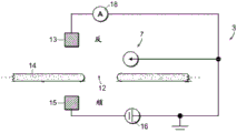
FIG. 1A is a schematic circuit diagram of a first embodiment nanopore sensor structure for determining local potential;
FIG. 1B is a circuit diagram of an embodiment transistor implementation of the nanopore sensor structure of FIG. 1A;
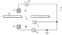
FIG. 1C is a schematic circuit diagram of a second embodiment nanopore sensor structure for determining local potential;
FIG. 1D is a circuit diagram of an example transistor implementation of the nanopore sensor structure of FIG. 1C;
FIG. 1E is a circuit diagram of an embodiment transistor implementation of a combination of the sensor structures of FIGS. 1A and 1C;
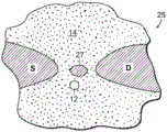
FIG. 1F is a schematic plan view of a single-electron transistor embodiment of a nanopore sensor structure for determining local potentials;
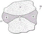
FIG. 1G is a schematic plan view of an embodiment of quantum dot contact for a nanopore sensor structure for determining local potential;
figure 1H is a schematic side view of a lipid bilayer including a fluorescent dye arranged as an embodiment of a protein nanopore sensor structure for determining local potentials;
FIG. 2A is a schematic diagram of a nanopore sensor structure and corresponding circuit elements for determining local potentials;
FIG. 2B is a circuit diagram of the nanopore sensor transistor embodiment of FIG. 1B;
FIG. 3A is a schematic side view of the geometric features of a nanopore sensor structure as defined for determining local potential for sensor quantitative analysis;
FIGS. 3A-3B are respectively a configuration for a fluid solution in which the cis and trans reservoirs comprise equal ionic concentrations and for a cis reservoir: (cisreservoir) and reserve reservoir (transreservoir) comprises a structure of a fluid solution of unequal ionic concentration, where the potential in the nanopore of the nanopore sensor for determining the local potential is plotted as a function of the distance from the nanopore into the cis reservoir;
FIGS. 3D-3E are plots of electric fields in a nanopore for a nanopore sensor for determining local potentials, corresponding to plots of potentials of FIGS. 3A-3B, respectively;
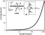
FIG. 4A is a graph of the change in potential for electrophoretic species translocation in a nanopore as dsDNA molecules translocate through the nanopore for a 50nm thick nanopore membrane and a 1V transmembrane voltage (TMV) structure, C for different nanopore diameters below 10nm as nanopore configuration for local potentiometryCis-trans/CInverse directionA plot of a function of ion concentration ratio;
FIG. 4B is a plot of the potential change in the anti-reservoir for a 10nm diameter nanopore at 1V TMV for the conditions plotted in FIG. 4A;
FIG. 4C is a plot of noise sources and signals as a function of recording bandwidth for a nanopore sensor configured for local potentiometry;
FIG. 4D is a plot of bandwidth of a nanopore sensor configured for local potentiometry as a function of cis-chamber solution concentration for a range of reservoir solution concentration ratios;
FIG. 4E is a plot of signal decay length from a nanopore site in a nanopore configured for local potential determination as a function of cis and trans reservoir solution concentration ratio;
FIG. 5 is a schematic diagram of a nanopore sensor comprising a fluidic channel connected between a first reservoir (here an anti-reservoir) and a nanopore in a support structure;
FIG. 6 is a circuit model of the nanopore sensor of FIG. 5;
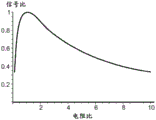
FIG. 7 is a plot of measured transconductance signal to maximum achievable transconductance signal ratio as a function of the ratio between fluid channel resistance and nanopore resistance;
FIG. 8 is a schematic side view of the nanopore sensor of FIG. 5 with a definition of geometric parameters;
FIG. 9 is a plot of the ratio of the resistance of a fluid channel to the resistance of a nanopore in the sensor of FIG. 5 as a function of the ratio of the diameter of the fluid channel to the length of the fluid channel for a selected sensor size;
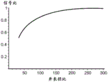
FIG. 10 is a plot of a ratio of measured transconductance signal to maximum achievable transconductance signal as a function of a ratio of fluid channel diameter to fluid channel length for a selected sensor size;
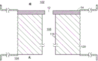
FIG. 11 is a schematic side view of a first fluid passageway structure;
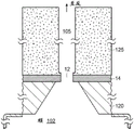
FIG. 12 is a schematic side view of a fluidic channel disposed on a support structure for a nanopore;
FIG. 13 is a schematic side view of an anodized aluminum oxide fluid channel structure;
FIG. 14 is a schematic side view of a transverse fluid channel structure;
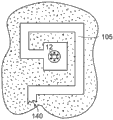
15A-15B are schematic top views of example lateral fluid channel structures;
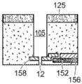
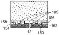
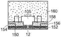
FIGS. 16A-16E are schematic side views of fluid channel structures arranged with elements for performing local potential measurements;
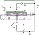
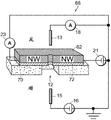
FIG. 17 is a schematic diagram of a nanopore sensor with nanowire FETs arranged on a thin film configured for local potentiometry;
FIG. 18 is a perspective view of an exemplary embodiment of the nanopore sensor structure of FIG. 17;
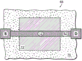
FIGS. 19A-19B are a schematic diagram and a plan view of an exemplary embodiment of a nanopore sensor with nanowire FETs arranged on a graphene thin film, respectively, configured for local potentiometry;
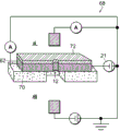
FIGS. 20A-20B are a schematic diagram and a plan view of an example embodiment of a nanopore sensor having a graphene layer disposed on a nanowire FET, respectively, configured for local potentiometry;
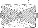
FIGS. 21A-21B are a schematic diagram and a plan view of an exemplary embodiment of a nanopore sensor with graphene thin film constructed for local potentiometry, respectively;
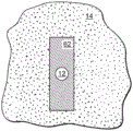
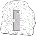
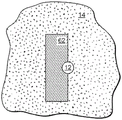
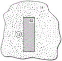
FIGS. 22A-22D are schematic plan views of example locations for nanopores of nanowires in a nanopore sensor configured for local potentiometry;
FIG. 23 is a plot of the sensitivity of nanowires in a nanopore sensor configured for local potentiometry before and after nanopore formation at the nanowire location;
FIG. 24A is a plot of i) measured ionic current through a nanopore and ii) measured nanowire FET conductance as DNA translocates through the nanopore in a nanopore sensor configured for local potentiometry for 2V TMV and a 100:1 cis/trans reservoir solution concentration ratio, respectively, for local potentiometry in a reserve reservoir;
FIG. 24B is a plot of i) measured ionic current through a nanopore and ii) measured nanowire FET conductance as DNA translocates through the nanopore in a nanopore sensor configured for local potential measurements performed in a reserve reservoir for 2.4V TMV and 100:1 cis/trans reservoir solution concentration ratios, respectively;
FIG. 24C is a plot of i) measured ionic current through a nanopore and ii) measured nanowire FET conductance for 0.6V TMV and 1:1 cis/trans reservoir solution concentration ratio, respectively, for local potentiometry in a reserve reservoir while DNA translocates through the nanopore in a nanopore sensor configured for local potentiometry; and is
Fig. 25 is a plot of i) the total ionic current measured through the three nanopores, ii) the measured nanowire FET conductance through the first nanopore, ii) the measured nanowire FET conductance through the second nanopore, and ii) the measured nanowire FET conductance through the third nanopore, respectively, as DNA translocates through the nanopores of the three sensors in a nanopore sensor configured for local potential measurement.
Detailed description of the invention
Fig. 1A-1E are schematic diagrams of nanopore sensor structures provided herein that enable a local potential sensing method for nanopore sensing. For clarity of discussion, features of the devices shown in the figures are not shown to scale. Referring to fig. 1A, fig. 1A shows a nanopore sensor 3, the nanopore sensor 3 comprising a support structure 14, such as a thin film, in which a nanopore 12 is arranged. The nanopore 12 is configured in a support structure between two fluid reservoirs, shown schematically as a cisreservoir and a cisreservoir, such that the nanopore 12 is the only fluid communication channel between the cisreservoir and the cisreservoir. One reservoir is connected to the inlet to the nanopore and the other reservoir is connected to the outlet from the nanopore. In nanopore sensor operation for local potentiometric detection of translocation of a substance through a nanopore, one or more substance objects, such as molecules, are provided in a fluid solution within one of the reservoirs for translocation through the nanopore to the other of the two reservoirs. For many applications, particularly for molecular sensing applications, molecules or other objects of matter may preferably be provided in an ionic fluid solution in one of the reservoirs, and may be provided in either reservoir.
Objects of matter to be translocated through a nanopore may include objects selected from, for example, DNA fragments, RNA fragments, PNA, nucleotides, nucleosides, oligonucleotides, proteins, polypeptides, amino acids, and polymers. The material object may include a tag that is released from the labeled nucleotide. By means of a polymerase, nucleotides along a nucleic acid molecule may be polymerized to produce a strand of nucleic acid complementary to at least part of the nucleic acid molecule, whereby during polymerization the tags are released from individual nucleotides of the nucleotides, whereby the released tags move through the nanopore, as described in WO 2013/191793, incorporated herein by reference.
The nanopores may be provided as holes, gaps, channels, trenches, holes or other apertures in the support structure, the nanopores having a certain extent, e.g. diameter, for a corresponding geometry suitable for the object of interest for the sensing substance. For sensing translocation of molecules through a nanopore, nanopores of less than about 100nm may be preferred, with nanopores of less than 10nm, 5nm, or 2nm being more preferred. As discussed below, 1nm nanopores may be suitable and more preferred for some molecular sensing applications.
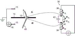
The reservoirs or other components of the nanopore sensor may be configured to provide a driving force for the movement of a substance object (e.g., a molecule) toward the nanopore or from one reservoir to another through the nanopore. For example, electrodes 13,15 may be provided in a circuit with voltage and current elements 16,18 to provide electrophoretic forces between the reservoirs for electrophoretically driving a substance in solution from one reservoir to the other toward or through the nanopore. To enable electrophoretic driving of the species, the fluid solution of the reservoir may be provided as a solution of electrically conducting ions having a pH and other characteristics suitable for the species in solution. Thus, the circuit may be connected in series with the reservoir solution through the nanopore using the electrodes 13,15 shown in the figure, thereby providing a voltage bias between the solutions across the nanopore. Translocation of substances through nanopores and rate of translocation control can be carried out using alternative techniques, such as enzymatic molecular motors.
In addition to or instead of a driving force for applying a voltage, a pressure gradient across the pore may be used to bring the molecule to and/or through the nanopore. The pressure gradient may be created by using physical pressure or chemical pressure (e.g., osmotic pressure). Osmotic pressure can result from the difference in concentration across the cis and trans chambers. By having an osmotic active agent concentration gradient, such as salt, polyethylene glycol (PEG), or glycerol, osmotic pressure can be generated.
As shown in fig. 1A, a conversion element 7 may be provided in the nanopore sensor, the conversion element 7 sensing a potential local to the element site and displaying a feature indicative of the local potential. An electrical connection, for example a device or a region of a device and/or a circuit, a line or a combination of circuit elements sensing the local potential of the device and/or the circuit site, may be provided as the conversion element 7 to display a signal indicative of the local potential. The location of potential sensing may be in the reservoir, or on the surface of the support structure, or other location within the nanopore sensor, as described in detail below.
As shown in fig. 1B, a circuit 20 may be provided that includes, for example, a transistor device 22, the transistor device 22 having a source S, a drain D, and a channel region 24. In this example, the channel region 24 is physically disposed at a location in the nanopore sensor environment for local potentiometry. This physical location of the transistor channel region 24 may be at any convenient and suitable location for accessing local potentials.
In the arrangement of fig. 1A-1B, the potential sensing circuit is arranged in the anti-reservoir region to provide a transistor or other means of determining the potential of the anti-reservoir region on the anti-reservoir side of the nanopore 12. Alternatively, as shown in fig. 1C, an electrical conversion element 7, such as a potential sensing device or circuit, may be arranged on the downstream reservoir side of the nanopore. Here, as shown in fig. 1D, a circuit 20 may be provided, the circuit 20 including a transistor 24 on the parareservoir side of the nanopore 12 or other means of measuring the potential local to the parareservoir.
In another alternative arrangement, as depicted in FIG. 1E, two or more conversion elements may be included and have circuits 20a, 20b, etc. connected to the conversion elements, e.g., transistors 22a, 22b, which sense electrical potentials at two or more locations in the nanopore sensor system, e.g., on each side of the nanopore support structure. This arrangement can thus be used to determine the potential on both sides of the nanopore membrane 14, depending on the physical implementation of the potential sensing circuit. This is an example structure in which the local potential difference between two sites in a nanopore sensor can be determined. Thus, the term "measured local potential" is intended to refer to the potential at a single site in the nanopore sensor, the local potential difference or sum between two or more sites, and to the local potential at two or more sites in the nanopore sensor structure.
The local potential measurement may be performed by any suitable means and/or circuitry or other conversion element, including biological or other non-solid state conversion elements, and is not limited to the transistor embodiments described above. As shown in fig. 1F, a switching element configured as a single-electron transistor (SET) circuit 27 may be provided on the support structure 14. The source S and drain D regions of the SET are disposed on the support structure to provide a tunneling barrier for the SET 27. In the resulting quantum dot system, the conductance through the SET 27 depends on the energy level of the SET relative to the fermi levels of the source S and drain D. With the nanopore 12 adjacent to the SET, the potential and corresponding energy level of the SET changes as the object of matter is displaced through the nanopore, which changes the conductance of the SET circuit.
In addition, as shown in fig. 1G, a Quantum Point Contact (QPC) system 29 for performing local potential measurement may be provided on the support structure 14. In this system, a conductance region 31 is provided, forming a source S and a drain D, connected by a thin conductance channel region at the nanopore 12 site. The channel region is sufficiently thin to quantize the electronic carrier particle energy state perpendicular to the channel region. As the object of matter translocates through the nanopore, the local potential around the QPC and hence the fermi level within the thin conductance channel region changes, resulting in a change in the number of quantized states below the fermi level, with a corresponding change in QPC conductance.
Nanowire FETs can also be disposed at nanopore sites. The nanowires may be formed of any suitable electrically conductive or semiconducting material, including fullerene structures and semiconducting wires. The term "nanowire" as used herein refers to an electrical conduction channel characterized by a width compatible with the signal decay length measured from the nanopore site. The channel width is preferably in the same order of magnitude as the attenuation length and may be larger. The nanowires can be made of any semiconductor material that is stable in the selected reservoir solution.
The nanopore sensor is not limited to a solid state nanopore structure with a solid state voltage sensing device. Biological nanopores and potentiometric sensing arrangements may also be utilized, for example, protein nanopores or other suitable structures. As shown in fig. 1H, an amphiphilic layer 31 may be provided in which protein nanopores 33 are disposed. A voltage sensitive dye, for example, a fluorescent direct dye 37, may be provided in the lipid bilayer as an electrical conversion element. With this arrangement, as a species object, such as a molecule, translocates through the protein nanopore, the voltage drop across the amphiphilic layer changes and modulates the fluorescence of the dye by changing the voltage. Optical detection or sensing of dye fluorescence and changes in fluorescence provide sensing at the nanopore potential. This potentiometric determination can be performed with optical microscopy or other conventional arrangements as the optical output signal from the nanopore sensor. Such amphiphilic layer nanopore sensors are examples of biological nanopore sensors based on sensing local potentials at sites in the nanopore system. The local potentiometric approach to nanopore displacement detection is not limited to a particular solid state or biological structure, and may be applied to any suitable nanopore structure.
The support structure may be formed from one or both of organic and inorganic materials, including but not limited to microelectronic materials, whether electrically conductive, semi-conductive, or electrically insulating, including, for example, II-IV and III-V materials, oxides, and nitrides, such as Si3N4、Al2O3And SiO; organic and inorganic polymers such as polyamide, plastic (e.g., Teflon @) or elastomers (e.g., two-component addition-cured silicone rubber), and glass. The solid support structure may be formed from a single atomic layer, such as graphene, or a layer that is only a few atoms thick, as disclosed in U.S. patent 8,698,481 and U.S. patent application publication 2014/174927, both of which are incorporated herein by reference. More than one support layer material, e.g., more than one graphene layer, may be included, as disclosed in U.S. patent application publication 2013/309776, which is incorporated herein by reference. Suitable silicon nitride films are disclosed in U.S. patent 6,627,067, and the support structure may beChemical functionalization, as disclosed in U.S. patent application publication 2011/053284, both of which are incorporated herein by reference.
For the selected support structure material composition, thickness and arrangement, nanopores may be created in the support structure by any suitable method. For example, to create nanopores, electron beam milling, ion beam milling, engraving with energy beam materials, dry etching, wet chemical or electrochemical etching, or other methods may be utilized, as described in U.S. patent application publication 2014/0262820, U.S. patent application publication 2012/0234679, U.S. patent 8,470,408, U.S. patent 8,092,697, U.S. patent 6,783,643, and U.S. patent 8,206,568, all of which are incorporated herein by reference. Additionally, extrusion, self-assembly, deposition of material on the sidewalls of relatively large pores, or other nanopore formation methods may be utilized.
As an alternative to providing a completely solid-state nanopore, a biological nanopore may be provided within a solid-state pore. Such a structure is disclosed, for example, in U.S. patent No. 8,828,211, which is incorporated herein by reference. In addition, the biological nanopore may be a transmembrane protein pore. The biological pores may be naturally occurring pores, or may be mutant pores. Exemplary wells are described in U.S. patent application Ser. No. 2012/1007802, also described in Stoddart D et al, Proc Natl Acad Sci, 12, 106(19):7702-7, Stoddart D et al, Angew Chem Int Ed Engl. 2010, 49(3):556-9, Stoddart D et al, Nano Lett. 2010 Sep 8, 10(9):3633-7, Butler TZ et al, Proc Natl Acad Sci 2008, 105(52):20647-52, U.S. patent application publication 2014/186823 and WO2013/153359, all incorporated herein by reference. The pores may be homooligomeric, i.e., derived from the same monomer. The pores may be hetero-oligomeric, i.e., when at least one monomer is different from another monomer. The wells may be DNA folder wells, as described in Langecker et al, Science, 2012; 338:932-936, which is incorporated herein by reference.
In one embodiment, pores may be provided within the amphiphilic layer. The amphiphilic layer is a layer formed from amphiphilic molecules having both hydrophilic and lipophilic properties, such as phospholipids. The amphiphilic layer may be a monolayer or a bilayer and is selected from a lipid bilayer or a non-native lipid bilayer. Bilayers can be synthetic, as disclosed in Kunitake T., Angew. chem. int. Ed. Engl. 31(1992) 709-726. The amphiphilic layer may be a block copolymer as disclosed in Gonzalez-Perez et al, Langmuir, 2009, 25, 10447-10450 and U.S. patent No. 6,723,814, which are incorporated herein by reference. The polymer may be, for example, a PMOXA-PDMS-PMOXA triblock copolymer.
Referring to fig. 2A, any of these support structures, nanopores, and electrical structures that determine local electrical potentials at one or more sites in a nanopore sensor may be utilized in a method of sensing translocation of a substance through a nanopore. To explain the principle of such sensing, it is advantageous to model the nanopore sensor as a circuit 35, the circuit 35 comprising electrical components that correspond to the physical elements of the sensor, as shown in fig. 2A. The forward reservoir and the reverse reservoir can be respectively connected with a characteristic fluid access resistance R Inverse direction36、R Cis-trans38 are modeled. For this analysis, the access resistance is defined as the fluidic resistance of the reservoir solution local to the nanopore site, rather than the bulk solution away from the nanopore. Characteristic nanopore available nanopore solution resistance R Hole(s)40, i.e., the fluid resistance through the solution of the nanopore length between the two sides of the support structure in which the nanopore is disposed. The nanopore can also use the characteristic capacitance CHole(s)Modeling, which is the function of a thin film or other support structure in which the nanopores are disposed. The access resistance and nanopore solution resistance of both chambers are variables.
Under nanopore sensor initiation conditions where no species is translocated through the nanopore, the nanopore may be initially resistive by the solution resistance R given aboveHole(s)Characterised by the fact that the two fluid reservoirs can be respectively defined by the access resistances R of the trans-reservoir and the cis-reservoirInverse directionAnd RCis-transAnd (5) characterizing. Thus, as a matter object (e.g., biomolecule 45) moves through nanopore 12, as shown in FIG. 2A, the nanopore's solution resistance RHole(s)And the access resistance R of each reservoirInverse directionAnd RCis-transThe change is due to the molecule in the nanopore at least partially blocking a channel through the length of the nanopore, thereby changing the effective diameter of the nanopore. Upon such blockage, the fluidic solution resistance of the nanopore and the access resistance of both reservoirs both increase above the nanopore resistance and both in the absence of molecules in the nanoporeThe access resistance of each reservoir.
Partial clogging of the nanopore by the substance object differentially affects nanopore solution resistance and reservoir access resistance, as explained in detail below. Thus, partial clogging of the nanopore by the translocating substance results in a corresponding redistribution of voltage between the nanopore and the cis and trans reservoir solutions, and thus, a corresponding adjustment of the potential across the nanopore sensor site. Thus, the local potentials at the two sites labeled a and B in fig. 2A vary accordingly with this change in nanopore solution resistance and the voltage redistribution between the reservoir solution and the nanopore. Thus, a determination of a potential at any one of these sites or at another site of the nanopore sensor structure or a determination of a local potential difference between two or more sites indicates that the molecule translocates through the nanopore.
By means of the electrical conversion element arranged in the nanopore sensor, the local potential at the site of the selected nanopore sensor and the change in this potential can be sensed. For example, a change in conductance of a conductive channel in a transistor device may provide a potential measurement. Thus, the conductance of the transistor channel can be used as a direct indication of the local potential at the physical location of the transistor channel. The nanopore sensor arrangement of FIGS. 1A-1B corresponds to the local potentiometric determination of site A in circuit 35 of FIG. 2A. The nanopore sensor arrangement of FIGS. 1C-1D corresponds to the local potentiometric determination of site B in circuit 35 of FIG. 2A. The nanopore sensor arrangement of FIG. 1E is equivalent to the local potential measurement at both sites A and B in the circuit 35 of FIG. 2A, and is capable of measuring the potential difference at those two sites.
A circuit equivalent to the exemplary structure of fig. 1B is shown in fig. 2B. The connection resistances R of the forward and reverse reservoirs are shown here in each caseCis-trans、RInverse directionAnd a fluid solution resistance R of the nanoporeHole(s). The position of the electrical conversion element that determines the local potential, e.g. the channel of transistor 22, is here located at site a in fig. 2A, thereby providing an indication of the local potential of the anti-reservoir at the nanopore anti-reservoir side. With this arrangement, potentiometric measurements can be monitored as objects of matter, such as molecules, translocate through the nanopore, with respect to changes in potential (corresponding to changes in nanopore state) and the presence or absence of one or more objects in the nanoporeThe fixed circuit outputs a signal.
Such an analysis may be applied to any nanopore sensor in which local electrical conversion elements are provided. The analysis is not limited to FETs and other embodiments described above, but may be applied to any suitable arrangement of any conversion elements. It is all that is required to provide an electrical conversion element, such as a device, a device region, a circuit or other conversion element that performs local potential measurements as the matter object moves through the nanopore.
To further analyze nanopore sensor system parameters, the nanopore sensor may be modeled, as shown in the schematic of fig. 3A. To be able to analyze the calculations, several assumptions may be utilized. First, geometric changes in the nanopore support structure caused by the inclusion of local potential sensing transducing elements, such as the membrane and the nanopore itself and other areas of the nanopore sensor, can be ignored, and the potential sensing transducing elements can be modeled as point potential detectors. The fluid reservoir is assumed to contain a solution of electrically conducting ions. The two reservoir solutions are specified to include different ion concentrations, which may be different ion concentrations. In one analysis, the ion concentration profile through the nanopore system was determined by steady state diffusion driven by the cis/trans reservoir concentration difference, with different ion concentrations specified for the reservoirs, and the diffusion was assumed to reach steady state. Another assumption can be made by approximating a constant buffer concentration profile and potential in the small hemisphere on both sides of the nanopore. The nanopore sensor is assumed to be in a steady state. Under these conditions, the diffusion equation for a nanopore sensor is given by:
where C is the fluid ion concentration, t is the time, r is the position of the point in the reservoir measured from the nanopore, and z is the distance through the nanopore length. C = C away from the nanopore in the cis reservoir if these diffusion equations are solved under boundary conditionsCis-transAway from the nanopore C = C in the anti-reservoirInverse directionWhere the flow is at the nanopore and is the same for both reservoirs, and the concentration is continuous at the nanopore opening at each reservoir, then the ion concentrations of both reservoirs and the nanopore can be given as:
here, l and d are the thickness and nanopore diameter of the nanopore support structure, respectively. Thus, since the ion concentration profile is known, and the solution conductivity is proportional to the concentration, the conductivity σ of the solution is given by:
here, Σ is the molar conductivity of the solution. Assuming total current I, using the parastorage voltage VCReverse reservoir voltage VTAnd nanopore voltage VPThe potential drop across the nanopore sensor can be given by:
if these three equations are solved under boundary conditions, specifying that the potential away from the nanopore in the parareservoir is equal to the voltage applied across the structure or membrane, i.e., the transmembrane voltage (TMV), that electrophoretically drives the object through the nanopore, and away from the nanopore in the reverse chamber, 0V, then the voltage in the nanopore sensor (i.e., the voltage in the parareservoir) VC(r) voltage in the anti-reservoir VT(r) and voltage in nanopore VP(r) is given as:
since the potential is continuous at both nanopore openings into the reservoir, and since the total voltage applied is V, expression (5) can be further simplified to:
by this expression, the electric field E in the nanoporeP(r) can be given as:
with this expression, changing the potential by reducing the nanopore area a by the presence of a substance object (e.g., a molecule) in the nanopore, the potential change on the nanopore anti-reservoir side can be estimated as:
here, a is the cross-sectional area of the molecule. Based on the above expression of the voltage drop across the reservoir and nanopore, the resistance of the nanopore sensor, i.e., R, can be calculatedCis-trans、RInverse directionAnd RHole(s)The method comprises the following steps:
thus, the total resistance and ionic current of the nanopore sensor are given by:
with these expressions, it is demonstrated that the electrical properties of the nanopore sensor, in particular, the distribution of the electrical potential in the sensor, are directly dependent on the ionic concentration of the fluid solution in the cis and trans reservoirs. In particular, the reservoir solution concentration ratio directly affects the magnitude of the change in local potential due to the nanopore's mass translocation.
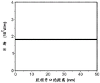
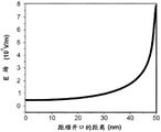
Figures 3B-3E are plots of the potential and electric field in the nanopore showing these conditions. Assuming a cis/trans buffer solution concentration ratio =1:1, 50nm thick nitride film, 10nm diameter nanopores in the film, and 1V transmembrane voltage, i.e., 1V applied between the solutions in the two reservoirs, the potential in the nanopores is plotted as a function of the distance from the nanopore opening in the cis reservoir, based on the above expression (6) in fig. 3B. The same potential is plotted in fig. 3C for the conditions in which the concentration ratio of the cis/trans buffer solution is 100: 1. It should be noted that at points near the lower concentration reservoir, the potential increases at a given nanopore location for the ratio of the unbalanced buffer solution.
Figure 3D is a plot of the electric field in the nanopore under the conditions given above for the equilibration buffer solution ratio based on expression (7) above. The same electric field distribution is plotted in fig. 3E for the condition in which the concentration ratio of the cis/trans buffer solution is 100: 1. It should be noted that at points near the low concentration, higher resistance reservoir, the potential increases for the unbalanced buffer solution than at a given nanopore location, and the electric field is significantly stronger.
From this result, it was found that the access resistance R to the reservoirs was made use of the condition in which the reservoir solutions were all provided as the same ion concentration conductivity ion solutionCis-transReverse storage access resistance RInverse directionAnd solution resistance R of the nanoporeHole(s)The ratio is fixed and the nanopore resistance is much larger than the memory access resistance. But under the unbalanced ion concentration condition, the reservoir with the lower ion concentration has a larger access resistance, which can be at the nanopore resistance level, while the higher ion concentration reservoir resistance becomes relatively negligible.
Based on this corresponding recognition, it was found herein that in order to maximize local potential measurements in nanopore sensors, in one embodiment, ion reservoir solutions having different ion concentrations may be provided. With this arrangement of the concentration of unbalanced ions, local potential measurements are preferably made at sites in the reservoir that comprise lower ion concentrations. More preferably, the buffer solution of the lower ion concentration solution is selected to give an access resistance to that reservoir that is the same as the nanopore resistance but of an order of magnitude much greater than the higher ion concentration solution resistance, e.g., at least of an order of magnitude greater than the high ion concentration solution, e.g., in order to, if the local potential measurement is performed in a back reservoir:
RT, RP>>RC (11)
thus, based on this finding, for setting the nanopore resistance RPGiven nanopore diameters, it is preferred in one embodiment to reduce the ionic solution buffer concentration of a reservoir designated for local potential measurements to a level at which the access resistance of that reservoir is of the same order of magnitude as the nanopore resistance. This reservoir accessThe resistance should not dominate the nanopore sensor resistance, but should be at the nanopore resistance level.
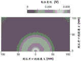
This condition can be directly quantitatively determined by electrical modeling of the nanopore sensor assembly in the manner described above. Based on the above expression (8), the solution concentration ratio at which the potential change reaches the maximum during the translocation of the selection object nanopore can be determined for the given nanopore sensor parameter. Figure 4A is a plot of the expression for electrophoretic species translocation as dsDNA molecules translocate through the nanopore for a 50nm thick nanopore membrane and a 1V TMV structure (8). The potential change is shown for different nanopore diameters C below 10nmCis-trans/CInverse directionIon concentration ratio. From this plot, it was found that for any nanopore diameter modeled here, the local potential change in the anti-reservoir was 100:1CCis-trans/CInverse directionThe chamber buffer concentration ratio is maximized. FIG. 4B is for selected 100:1CCis-trans/CInverse directionPlot of solution concentration versus corresponding calculated potential change distribution in the anti-reservoir for 10nm diameter nanopores at 1V TMV.
This demonstrates, based on the findings herein, that in one embodiment, for a given reservoir site selected for conducting a potential assay, the ionic fluid buffer concentration ratio in the two reservoirs can be selected using a lower buffer concentration solution in the assay reservoir to maximize the magnitude of the potential change at that selected assay site. Such a potential change distribution caused is highly localized to the nanopore of several tens of nanometers as shown in fig. 4B. For 100:1CCis-trans/CInverse directionThe solution concentration ratio, and the nanopore parameters given immediately above, can be determined based on the expression (9) above, that the solution resistance into the anti-reservoir and the solution resistance of the nanopore are indeed within the same order of magnitude.
With this reservoir fluid solution buffer concentration arrangement and potentiometric arrangement, it is noted that the local potential sensing technique produces a local potentiometric signal that is dependent on the transmembrane voltage (TMV) and ionic current signal. Other nanopore-based sensor technologies generally rely on direct interaction between the translocating substance and the nanopore sensor through, for example, electrical coupling or quantum mechanical tunneling. For these techniques, the nanopore output signal is generally not directly correlated to TMV or ion current, and should not change significantly as TMV changes. In contrast, in the local potentiometric system herein, the nanopore sensor signal is proportional to TMV and can be considered as a linear amplification of the ion current signal. Thus, both the local potentiometric signal and the ionic current signal amplitude depend linearly on TMV, but the ratio between them is constant for a given nanopore geometry and reservoir solution concentration, as evidenced by the expression given above.
The advantage of the local potential measurement method is the characteristic high bandwidth capability of the low noise measurement. The low signal bandwidth is one of the problems that direct nanopore sensing by conventional ionic current occlusion assay techniques is limited due to the difficulty of high bandwidth amplification of very small assay current signals. This may be particularly true for small nanopores when used for DNA sensing. In the local potential sensing method, a large local potential signal is measured instead of a small current signal, and therefore, the signal bandwidth is not limited by the current amplifier capability. Thus, high bandwidth signal processing electronics can be integrated onto the solid state nanopore sensing structure.
In addition, in addition to the intrinsic shot noise and johnson noise, the majority of the noise contributing to the ion current blockage measurement technique is introduced by capacitive coupling across the nanopore membrane, which portion of the capacitive coupling of noise dominates over certain stages of nanopore operation. To minimize noise, conventionally a small membrane area is required to be exposed to the reservoir solution. In the local potentiometric methods herein, because the local potentiometric signal decays within tens of nanometers for reasonable reservoir concentrations than around the nanopore, the local potentiometric signal is only affected by capacitive coupling between the reservoir solutions within the local volume. Therefore, most of the capacitively coupled noise is automatically rejected in the local potentiometric sensing method.
Referring to fig. 4C-4D, in one embodiment, the reservoir buffer solution concentration ratio may be selected to optimize the signal bandwidth of the nanopore sensor. Assuming local potential measurements are to be made on one side of the nanopore, assuming on the opposite side of the nanopore, the cisternal solution concentration is set reasonably high, e.g., about 4M, near the saturated solution, to maximize nanopore solution resistanceThe limit is reduced. Then, for example, based on the plot of fig. 4C, the signal noise is analyzed as a function of bandwidth. Various contributions to noise and signals expected for fluid nanopore manipulation are plotted here. The plot labeled "free space" refers to calculations based on free space molecular size. The plot labeled "Bayer" refers to molecular size-based calculations from previous papers by Bayer et al, in J. Clarke et al, "Continuous base identity for Single-Molecule Nanopore DNA Sequencing" (sequential base recognition for Single-Molecule Nanopore DNA Sequencing), Nature Nanotechnology, N.4, pp.265-270, 2009. The two signal lines are the smallest signal difference achieved between the four DNA bases, this smallest signal being present between the A and T bases. Here, the nanopores are given as 1nm diameter nanopores in a graphene thin film, with a 4M cisreservoir solution concentration, a buffer concentration ratio between 50:1 reservoirs, and about 10-9V/√ Hz voltage noise density. The dielectric loss tangent of graphene is unknown, and therefore, 1 is used for convenience. It was found that the intersection of the signal and the total noise in the plot set the 1:1 signal-to-noise ratio (S/N). This is the highest possible signal bandwidth. For example, for fluidic nanopore operation, the 1: 1S/N ratio is at about 100MHz bandwidth. Bandwidths greater than about 50MH and 100MHz bandwidths may be preferred.
Referring to the plot of fig. 4D, the 100MHz bandwidth corresponds to about a 50:1 reservoir solution concentration ratio, where the local potential measurements are made on the low concentration reservoir side of the nanopore. For the nanopore sensor parameters used in this example, any reservoir concentration ratio above about 50:1 will reduce the bandwidth. Any concentration ratio below about 50:1 will reduce the signal-to-noise ratio. Thus, it is found herein that the bandwidth can be optimized and there exists a reservoir concentration ratio optimization point, i.e., 50: 1. In one implementation, the reservoir solution concentration ratio may be selected based on a tradeoff between the characteristic noise of the nanopore sensor and the desired operating bandwidth of the nanopore sensor. Thus, it will be appreciated that to minimize noise, the reservoir solution concentration ratio may be increased, but the bandwidth may be decreased accordingly. Alternatively, electronic signal processing (e.g., low pass filtering) or other signal processing may be utilized.
It will also be appreciated that for a given material object to translocate through a nanopore, generally smaller diameter nanopores produce larger signals. However, for applications such as sensing of specific molecules (e.g., DNA), nanopore extent is preferably based on molecular extent, and reservoir concentration ratio is adjusted accordingly.
In another embodiment, the reservoir buffer solution concentration ratio may also be selected to produce a signal decay length that accommodates the selected local potentiometric device from the nanopore site assay. It will be appreciated that the decay length of the signal should be large enough to accommodate the potentiometric device arrangement within the decay length. Fig. 4E is a plot of signal decay length for a range of buffer concentration ratios, assuming local potential measurements are to be performed on the anti-reservoir side of the nanopore. The drawing is based on the circuit model shown in the inset in the drawing.
Based on this analysis, it was shown that at concentration ratios greater than about 20 or 30, sufficient signal decay length was generated to accommodate devices capable of measuring local potentials within the decay length. Providing a sufficient decay length at a concentration ratio greater than about 50:1 for local potential measurements within the decay length. Signal attenuation lengths greater than about 5nm and, for example, signal attenuation lengths of about 10nm and about 20nm may be preferred.
This particular embodiment of the determination of relative cis and trans solution ion concentrations using nanopore sensor analysis is based on the consideration of nanopore resistance and reservoir access resistance changes caused by the translocation of species through the nanopore. The methods herein provide further analysis, methods, and structures that additionally account for the change in fluid resistance of the cisreservoir and the cisreservoir immediately distal from the nanopore during translocation of the substance.
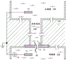
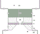
Referring to fig. 5, a nanopore sensor 100 provided herein is schematically shown in this further embodiment, the nanopore sensor 100 comprising a cis reservoir 102 and a trans reservoir 104 on opposite sides of a nanopore 12 arranged in a support structure 14. The nanopore must pass through a fluid communication channel between the two reservoirs. A fluid channel 105 is disposed between one reservoir (shown here as an anti-reservoir) and the nanopore 12 to fluidically connect that reservoir to the nanopore via the fluid channel. The fluidic channel has a channel length that is greater than the channel cross-sectional extent, width, or diameter, and is connected to enable fluid communication between the nanopore and a reservoir to which the channel leads. A second reservoir, here a paramagnetic reservoir, is arranged for communication with the fluid channel via the nanopore. The second reservoir need not include a second fluid passageway.
As with the nanopore sensor example described above, the nanopore sensor 100 of the present embodiment may comprise electrodes 13,15 and a voltage source 16 for applying an electrical potential across the solid support structure between the reservoirs. The nanopores are arranged in a suitable support structure, either solid state, biological, or some combination of the two in the manner described above.
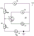
The nanopore sensor embodiment may be electrically modeled as shown in the circuit of fig. 6. In this model, the aspect ratio of the nanopore (i.e., the ratio of the nanopore diameter to the length) and the aspect ratio of the fluidic channel are assumed to be large enough so that the fluidic access resistances of the anti-reservoir and the pro-reservoir chambers can be neglected. Then defining the resistance R of the fluid channelFPAnd a nanopore resistance RHole(s). Also assume that the fluid resistance R of the fluid channelFPMuch greater than the overall fluid resistance of the cis reservoir and also much greater than the overall fluid resistance of the trans reservoir. Thus, as shown in fig. 6, the nanopore sensor resistance may be modeled as a fluid channel resistance and a nanopore resistance.
Referring to both fig. 6 and 5, an electrical conversion element 7 as described above is provided in the sensor to sense the electrical potential local to the fluid channel 105 and display a characteristic indicative of the local electrical potential in the fluid channel. An electrical connection, such as a device or region of a device and/or a circuit, a line, or a combination of circuit elements that sense a local potential of a device and/or a circuit site, may be provided as a switching element to display a signal indicative of the local potential. The location of the electrical conversion element 7 may be in a reservoir, on the surface of a support structure, as shown in fig. 5, a location within a fluidic channel or other location within a nanopore sensor.
As shown in fig. 6, in one embodiment, a circuit 20 may be provided for supporting an electrical conversion element, i.e., for example, a transistor device having a source S, a drain D and a channel region. The channel region may be physically disposed at a location in the nanopore sensor environment for local potentiometry. This physical location of the transistor channel region can be at any convenient and suitable location for accessing the local potential.
Considering now this nanopore sensor arrangement, if the resistance of the fluidic channel 105 is comparable to the resistance of the nanopore 12, then with respect to the access resistance of one reservoir to the nanopore, as expressed by (11), local potentiometry of the fluidic channel maximizes the determination of the signal that the indicator substance translocates through the nanopore in the manner discussed above. The voltage V is sensed by measuring the local potential at the location shown in the circuits of FIGS. 5-6SensingGiven as:
wherein R isHole(s)Is the resistance of the nanopore, RFPIs the resistance of the fluid channel, V0Is the voltage 16 applied across the nanopore from the circuit.
Voltage signal V to be detected during translocation of a substance through a nanoporeSignalFor small voltage changes due to corresponding small resistance changes of the nanopores partially blocked by the translocating substance, VSignalGiven as:
This relationship demonstrates that if the fluidic channel resistance is not the same as the nanopore resistance, the detectable voltage signal is less than the maximum possible voltage signal. The ratio R between the actual voltage signal achieved and the maximum measured voltage signalSignalTells the system how far from the optimal conditions, the ratio index is given as:
expression (14) is plotted in FIG. 7. This plot shows that the voltage signal V is 10% of the nanopore resistance at the fluid channel resistanceSignalGreater than 30% of the maximum achievable signal. Therefore, for the purposes of this analysis, the resistance R in the fluid path will beFPIs a nanopore resistance RHole(s)Is not greater than about 10 times the nanopore resistance, is considered a fluidic channel resistance and nanopore resistance match.
To determine the structural and geometric requirements of the fluidic channel to meet these resistance matching requirements, in one example approach, it may be assumed that both the nanopore and the fluidic channel generally have cylindrical geometries. In addition, as described above, for this analysis, the access resistances of the cis and trans reservoirs can be ignored, assuming that the aspect ratio of the nanopore and fluidic channel is relatively high relative to the cis and trans reservoirs. Finally, it is assumed that the ion concentration between the cis and trans reservoirs diffuses in a steady state condition if the ion concentrations in the two reservoirs are different.
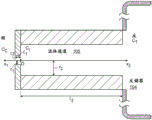
Fig. 8 is a schematic view of the geometry defining the fluid channel 105. Here, |1、r1And l2、r2Respectively, the length and radius of the nanopore and the fluidic channel. CC、CIAnd CTRespectively, the concentration of the ionic solution in the cis chamber, the concentration of the ionic solution at the interface between the nanopore and the fluidic channel, and the concentration of the ion in the trans chamber.
Under steady state conditions, the diffusion Flux of the ion concentration in the nanopore and the fluid channel is equal under the conditions:
thus, the interface concentration CICan be defined as:
thus, the ion concentration C in the nanoporeHole(s)And a fluidIon concentration C in the channelFPGiven as:
under normal measurement conditions, the conductivity σ of a solution is generally approximately proportional to the ionic concentration of the solution, and is:
where Σ is the molar conductivity of the solution and C is the ion concentration. Using this relationship, the resistance R of the nanoporeHole(s)And resistance R of the fluid channelFPGiven as:
the resistance ratio can then be determined from the expression (18) as:
By setting the ratio to the value 1 in expression (19), then:
to simplify this expression, the ion concentration ratio C in the cis and trans chambersC/CTCan be defined as RCRatio of radius of fluid channel to radius of nanopore r2/r1Can be defined as Rr. Aspect ratio AR of nanoporesHole(s)Can be defined as ARHole(s)=l1/r1Aspect ratio AR of fluid channelFPDefinable ARFP=l2/r2. Simplified representationThen the result is given as:
this expression directly shows that in order to match the fluidic channel resistance to the nanopore resistance, the aspect ratio of the fluidic channel must increase in proportion to the ratio of the fluidic channel radius to the nanopore radius. If the ionic concentration of the fluid solution in the cis and trans chambers is equal, the aspect ratio of the flow channel is set only by the ratio of the flow channel to the nanopore radius. If the ionic concentrations of the fluid solutions are not equal, the aspect ratio required for the fluid channel to satisfy this condition is reduced by a corresponding factor, assuming that a low concentration solution is provided in, for example, the fluid channel and the trans-chamber, and a high concentration solution is provided in the cis-chamber. In one embodiment, a large ion concentration ratio may be utilized consistent with the flow channel design in the manner described above to reduce the aspect ratio requirements for the flow channel while maintaining the impedance match between the flow channel and the nanopore.
Where manufacturing or other considerations do not allow for the creation of a fluidic channel having dimensions that substantially resistively match the nanopore, the above full ratio expression (14) may be considered, assuming all the variable relationships in the ratio are:
for an example of this relationship, if the diameter of the fluidic channel is 1000 times the nanopore diameter, e.g., 1.5 μm versus 1.5nm, for a nanopore length to nanopore diameter aspect ratio of 3:1, the aspect ratio of the fluidic channel is set to 300:1, here 450 μm deep, for the fluidic channel length to the fluidic channel diameter to match the nanopore resistance when a 100:1 ion concentration difference is utilized between the cis and trans chambers. This result is shown in the plot of fig. 9, where fig. 9 shows the assumed resistance ratio for a 3:1 aspect ratio nanopore, a 100:1 ion concentration difference, and a flow channel diameter of 1000 times the nanopore diameter.
Such perfect resistance matching is not required. As explained above, the voltage signal V is 10% of the nanopore resistance at the fluid channel resistanceSignalGreater than 30% of the maximum achievable signal. For example, assuming a fluid channel having a 50:1 aspect ratio with a 75 μm length, this may provide nanopore resistance>20% as shown in the plot of FIG. 9, and 60% of the maximum voltage signal can be obtained as shown in the plot of FIG. 10. Based on the resistance-voltage signal relationship, as shown in the plot of fig. 9, the fluid channel aspect ratio required to meet the performance specification for the nanopore sensor can be determined. Thus, no particular flow channel aspect ratio is required, as long as the channel length is greater than the channel diameter. All that is required is to arrange the electrical conversion element at some location in the nanopore sensor that is capable of determining the local potential of the fluid channel.
This nanopore arrangement, which includes a fluidic channel connected between the nanopore and one of the reservoirs, may offset some of the limitations caused only by the difference in the concentration of the cis and trans chamber ionic solutions. In nanopore sensors comprising different ion concentrations but no fluidic channel, the ion concentration affects the nanopore resistance and the cis-trans reservoir access resistance, and in this case, the ability of the nanopore resistance to match one reservoir access resistance is limited, thus limiting the voltage signal that can be generated. In addition, the fluidic access resistance is located near the nanopore and is a function of distance from the nanopore, and thus, there can be significant signal fluctuations for the movable electrical switching element, such as an amphiphilic thin film layer. The inclusion of a fluidic channel between the nanopore and one reservoir enables the structural definition of the fluidic resistance and the addition of additional control parameters to the nanopore sensor. The nanopore sensor can be tuned by controlling the length-diameter ratio of the fluid channel and the concentration of the cis-trans reservoir ionic solution so as to optimize the voltage signal determination.
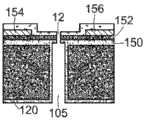
The fluidic channel connecting the reservoir to the nanopore may be constructed in any convenient arrangement that enables selection of aspect ratios and integration with the nanopore sensor. Referring to fig. 11, the fluidic channels 105 may also form wells, trenches, channels, or other fluid-containing chambers in the structure provided for defining the nanopore. For example, the fluidic channel may be a tube, channel, open channel, passageway, or other geometry in the structure 120 arranged with the support structure 14 in which the nanopore 12 is arranged. In this example, the support structure layer 14 is disposed on a substrate 120 for providing the nanopore 12. Fluid channels are formed in substrate 120. The walls 115 of the fluid channel may be configured to provide a suitable fluid channel cross-sectional geometry, such as a generally circular, oval, circular, square, or other geometry. The fluid channel is connected to a reservoir of any dimension, e.g. an anti-reservoir; the figures schematically show an anti-reservoir, showing that the anti-reservoir has any dimension and is not generally a high aspect ratio channel like a fluidic channel.
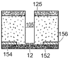
Referring to fig. 12, the fluidic channel 105 may be arranged opposite to the nanopore support structure. For example, a material layer 125 may be provided on the nanopore support structure 14, and the fluid channel 105 is defined in the material layer 125. A substrate or structure 120 supporting the nanopore support structure 14 may be provided opposite the fluid channel, on the opposite side of the support structure 14. The fluid channel structures of fig. 11-12 demonstrate that the fluid channel can be disposed at any convenient location on the nanopore sensor.
Referring to fig. 13, the fluid channels 105 may be provided as a set of holes, wells, channels, or other geometries in a selected arrangement. For example, the fluid channel 105 may include an Anodized Aluminum Oxide (AAO) layer. AAO is a conventional material that can be formed with very high aspect ratio pores, e.g., >1000:1, having a diameter of about 100 nm. These AAO pores are arranged in two dimensions in a quasi-hexagonal lattice with a lattice constant in the range of hundreds of nanometers. The aluminum oxide film can be anodized under controlled anodization conditions, such anodization being performed on the film with a surface pre-patterning to adjust the AAO lattice constant and pore diameter. The AAO pore groups work together to provide an effective aspect ratio. Such AAOs are arranged as examples of porous membranes, or other structures having pores, wells, passages, or other channel groups that can be used as fluid channels.
Additionally, any fluid channel structure may be filled with a gel or other porous substance or selected material disposed within the fluid channel to increase the fluid resistivity of the fluid channel.
The fluid channels may be configured in a vertical arrangement, a horizontal arrangement, or a combination of horizontal and vertical geometries. Referring to fig. 4, in one embodiment, fig. 4 schematically shows a fluidic channel comprising a vertical channel section 134 and a horizontal channel section 136. Such an arrangement may be provided, for example, in the surface layer 132 on the support structure 14, or may be integrated into a substrate or other structural element.
Referring to fig. 15A and 15B, the fluid channel 105 may be configured in any suitable passageway transverse or vertical geometry that selects the aspect ratio of the fluid channel. As schematically shown in fig. 15A, channels that spiral upon themselves laterally or vertically may be configured to achieve a selected fluid channel aspect ratio. As shown schematically in fig. 15B, a transverse or vertical serpentine channel may alternatively be used as the fluid channel. Without requiring a particular geometry, the fluidic channel may pass through a variety of materials and different support structural elements that connect between the reservoir and the nanopore. The geometry may be provided in a layer on a support structure, substrate or component assembly in the sensor. The ports 140 of the fluidic channel can be connected in a horizontal or vertical orientation to provide fluid communication between the liquid reservoir and the nanopore.
In various embodiments, these various fluid channel structures may include, for example, AAO films having pores with diameters of about 150nm, pore-to-pore distances of about 300nm, and film thicknesses between about 100 μm and 1000 μm; a planar PDMS/oxide/nitride channel having a width between about 0.5 μm and 1 μm, a depth between about 100nm and 200nm, and a length between about 200 μm and 500 μm; a deep well in the dielectric material having a well diameter between about 0.5 μm and 2 μm, and a diameter between about 20 μm and 50 μm; and a silicon wafer well having a diameter between about 2 μm and 6 μm and a depth between about 200 μm and 300 μm. In each of these embodiments, the concentration of the cis-trans ions may be the same or may be different, and the ion concentration ratio is selected, for example, to be between about 50:1 and 1000:1 as the ratio of the concentration of the cis-ion to the concentration of the counter-ion.
Turning to embodiments of a fluid channel having an electrical conversion element for performing local potential measurements in the fluid channel, as explained above, local potential measurements may be performed in a nanopore sensor using any suitable device or circuitry that accommodates the nanopore embodiments. Referring to fig. 16A-16E, the fluidic channel structure described immediately above may be adapted to include an electrical conversion element at the nanopore junction site to the fluidic channel. The structure of fig. 16A corresponds to the fluid channel design of fig. 11. Here, a substrate 120 having a buried oxide layer (BOX) and a silicon layer 152 provided on top thereof may be formed using a silicon-on-insulator (SOI) wafer. Nanopores 12 may be formed in these layers 150, 152. Silicon layer 152 may be configured as a conductive channel for local potential measurement at the nanopore site and provide conductive source 154 and drain 156 regions for measuring the conductance converted by the silicon conductive channel. Similarly, as shown in fig. 16B, the silicon layer 152 may be configured as an electrically conductive channel region having source and drain regions 154, 156, here in the layer 125 defining the fluid channel. As shown in fig. 16C, a sensing electrode 158 of metal, carbon nanotube or other material may be fabricated at the site of nanopore 12 and connected for sensing, for example, by drain electrode 156.
Referring to fig. 16D-16E, the figures show transverse fluid channel passageways with switching elements in cross-section. In the structure of fig. 16D, the fluid channel 105 is provided in a layer 158, for example, a nitride layer. A nitride layer 158 is provided on the support structure 14 with the underlying BOX layer 150, e.g., from the silicon layer 152 of the SOI wafer. The source and drain regions 154, 156 are connected to the silicon layer 152, and the silicon layer 152 is patterned into channels for switching the local potential at the nanopore. In the structure shown in fig. 16E, fluidic channels are provided in the top layer 160 (e.g., PDMS), shown in cross-section to depict channels, such as those in fig. 15A-15B. The channels may be molded into the top layer 160 and then connected to the nanopore sensor structure. The silicon layer 152 from the SOI wafer may be configured as a conductive via having source and drain regions 154, 156 connected for switching the local potential at the nanopore. These structures in fig. 16A-16E are each capable of sensing a local electrical potential in the fluidic channel of the nanopore.
For any nanopore sensor implementation, a range of additional electrical conversion elements may be utilized with or without a fluidic channel. For many applications, nanowire-based FET devices may be well-suited devices, but these are not required herein. SET, QPC, lipid bilayer or other devices and nanopore tools, whether biological or solid, may be utilized. Any circuit or device capable of measuring the local potential may be utilized.
In one example, a nanowire FET can be constructed in a nanopore site, as shown in fig. 17, without a fluid channel for clarity. In this nanowire embodiment 60, a nanowire 62 is provided on the support structure 14 in which the nanopore 12 is disposed. The nanowires may be formed of any suitable electrically conductive or semiconducting material, including fullerene structures and semiconducting wires. The term "nanowire" as used herein refers to an electrically conductive channel of a width characteristic that is compatible with the signal attenuation length measured from the nanopore site described above. The channel width is preferably in the same order of magnitude as the attenuation length and may be larger. The nanowires can be made of any semiconductor material that is stable in the selected reservoir solution.
Fig. 18 is a perspective view of an embodiment 65 of the nanopore sensor of fig. 6. Here, nanowires 62 are shown provided on the thin film support structure 14, the support structure 14 being self-supporting across its extent, just like a trampoline, between the support frames at the edges, provided on a support structure 64, such as a substrate. The nanowires are provided on a thin film having nanopores extending through the nanowires and the thickness of the thin film. As shown in fig. 17 and 18, the nanopore does not extend across the width of the nanowire. There is a region of the nanowire that is unbroken along the extent of the nanopore so that the conductance is continuous along the length of the nanowire. Metalized or other electrically conductive regions are provided at each end of the nanowire to form source (S) and drain (D) regions. With this configuration, a nanopore sensor can be constructed using cis-trans reservoirs and a fluidic channel connected to one of the reservoirs for detecting translocation of a substance from one reservoir to the other through the nanopore.
Referring also to fig. 19A-19B, the support structure and nanowire structure may be implemented in a variety of alternative arrangements, and for applications in which the nanowire material is self-supporting and may itself serve as a support structure in which nanopores are disposed, no support structure, such as a thin film support layer, is required. For example, as shown in fig. 19A-B, in a graphene-based nanopore sensor 68, a support layer 70 may be provided, which support layer 70 in turn supports a graphene thin film 72. Graphene film 72 is self-supporting across the pores in support layer 70. The graphene film in turn supports the nanowires 62, and the nanopores 12 extend through the nanowires and the graphene thickness, with the nanowires continuously remaining along some points of the nanowires. As shown in fig. 20A-20B, this arrangement may be varied, with the nanowires 62 arranged on the support layer 70 below the graphene layer 72.
In an alternative graphene-based nanopore sensor 75, as shown in fig. 21A-21B, a support structure, such as a support layer 70, may be constructed upon which is disposed a graphene layer 68, the graphene layer 68 serving to provide a structure in which the nanopore 12 is constructed and itself serving to provide a nanowire. The graphene may be provided in any suitable geometry that requires nanowires at the site of the nanopore 12. In this arrangement, due to its thickness and conductivity, the graphene layer 68 senses the local potential across the nanopore, i.e., the conductance of the graphene layer changes as a function of the local potential in the trans-cis two reservoirs. Thus, for the graphene-based nanopore sensor, the nanopore sensor signal of the local potentiometry is indicative of the cis-trans reservoir potential difference.
Thus, the potential local to the nanopore sensor fluid channel can be measured using any of a wide range of electrical conversion elements. A semiconductor-based FET or other sensing device, a sensing metal electrode connected to a device (e.g., a FET device), a graphene-based device, or other suitable switching element may be utilized.
As these arrangements demonstrate, the support layer, support layer thin film, nanowires, and support structure can be constructed with any of a wide range of material combinations and thicknesses. The fluid channel structure described above may be integrated into any of these arrangements. For many applications, the structure in which the nanopores are arranged may preferably be as thin as possible, and preferably not thicker than the extent of the object or object region of the substance to be detected. As explained above, the support structure material may comprise a nitride, oxide, conductor, semiconductor, graphene, plastic, or other suitable material, which may be electrically insulating or electrically conductive.
As shown in fig. 22A-22D, for the nanowire embodiment, nanopores are provided at the location of the nanowires 62 to provide unbroken, continuous channels for conductance through the nanowires. The nanopore may be provided in a central region of the nanowire, as depicted in fig. 22A, may be provided at an edge of the nanowire, as depicted in fig. 22B-22C, or may be provided in a location near or adjacent to the nanowire, as depicted in fig. 22D. In all cases, a continuous channel for electrical conduction is provided by the nanowires.
It was found in the nanopore arrangements of fig. 22A-22C that the sensitivity of the nanopore region was also significantly improved compared to the sensitivity of the same region prior to nanopore drilling. This sensitivity localization can be understood by interpreting the nanowire as a model of the reduction in cross-sectional area of the conducting channel, assuming that all other material properties remain unchanged, such as doping level and mobility. Reducing the nanowire cross-sectional area increases the resistance of the nanopore region, thus mitigating series resistance and signal attenuation from other portions of the nanowire. For a rectangular nanopore as an example, this sensitivity improvement in the nanopore region can be quantified from the following equation:
here, Δ is the sensitivity improvement, defined as the sensitivity of the device with the nanopore divided by the sensitivity without the nanopore, ρ0And ρ are the linear resistivities of the nanowire conductive pathways with and without nanopores, respectively. L is the total channel length, L0The channel length, which is the nanopore region, for this square example, is equal to the side length of the nanopore along the nanowire axis. For the other parts of the nanowire, the sensitivity should be slightly reduced after nanopore drilling, since all parameters remain the same, but the total channel resistance is slightly increased due to the nanopore. The combination of increased sensitivity in the nanopore region and decreased sensitivity in all other nanowire portions results in an increase in the sensitivity of the nanopore sensor, self-aligning and positioning in the nanopore.
In fabricating nanopore sensors, for embodiments including fluid channels and for embodiments not including fluid channels, first considering nanowire-based solid-state nanopore sensors, short channel nanowires may be preferred, and for many applications, silicon nanowires (SiNW) may be preferred, since SiNW has been demonstrated to be an excellent potential and charge sensor for subcellular and single virus-level signaling with significant stability in solution. To minimize signal attenuation from the channel series resistance, the SiNW channel can be reduced to less than about 200nm by solid state diffusion of nickel, if desired. SiNW may be produced by, for example, chemical vapor deposition or other suitable methods and disposed on a selected film, such as a nitride film, by solution. For many applications, commercially available nitride thin film chips may be suitably utilized. The source and drain can be created at the nanowire end using electron beam etching or photo etching. All electrodes and electrical contacts are passivated with, for example, a nitride or oxide material, which may be done after metal evaporation and before the lift-off process. The nanopore can be created at a selected site, for example, by an electron beam, or by creating other beam species or etching processes that select the size of the nanopore.
In fabricating graphene-based nanopore sensors comprising nanowire structures atop a thin graphene film, such as the graphene-based nanopore sensors of fig. 19A-19B, a thin film, such as a nitride thin film, is first processed to form micron-sized pores in the thin film, for example, by electron beam etching or photo etching and Reactive Ion Etching (RIE). Then, a graphene sheet or piece is disposed on the nitride thin film, covering the hole, to form a graphene thin film. Graphene sheets can be synthesized by CVD or other methods, or can be produced by mechanical exfoliation and transferred to a nitride film over the nitride film holes.
Electron beam etching or photo-etching may then be performed using metal evaporation to define electrodes on the nitride film in a conventional manner. The nanowires can be aligned in the position of the holes in the nitride film on top of the graphene film by electrophoresis or other suitable methods, such as silicon nanowires. Electron beam etching or photo etching can then be performed using metal evaporation to define source and drain contacts at the SiNW ends. Subsequently, excess graphite can be removed by e-beam etching or photo-etching and removing graphene from areas other than the intended graphene film locations, for example, by a UV-ozone stripper, oxygen plasma, or other suitable method. Finally, nanopores are created in the region of the nanowires and underlying graphene film, for example, by electron beam milling, ion beam milling, etching, or other suitable methods described above.
Graphene-based nanopore sensor including graphene thin film atop nanowire FET structure in fabrication20A-20B, the arrangement may be constructed using suitable structures, for example, using silicon-on-insulator (SOI). In this example, the hole is first formed through the back side thick silicon portion of the SOI chip, for example, through XF2Etching is stopped on the oxide layer to form a silicon oxide film. The oxide layer is then removed from the SOI wafer in the smaller hole area using electron beam etching or photolithography, creating a thin silicon film from the thin silicon area of the SOI wafer. The silicon thin film is then etched to form silicon nanowires, for example, using electron beam etching or photolithography and chemical etching or RIE. In one example, a dovetail-shaped Si wafer is formed, as shown in fig. 20B, aligned with the hole in the oxide film of the SOI wafer.
Electron beam etching or photo etching may then be performed using metal evaporation to define electrodes on the oxide layer in a conventional manner. Then, a graphene sheet or piece is disposed on the oxide thin film, covering the hole, to form a graphene thin film on the silicon nanowire. Graphene sheets can be synthesized by CVD or other methods, or can be produced by mechanical exfoliation and transferred to an oxide film, covering the SiNW and oxide film holes. It should be appreciated that the graphene sheets may not be flat due to the graphene sheets overlying the patterned silicon layer. If leakage is a problem with this arrangement, the graphene edge may be coated with, for example, SiOxA thin layer to form a sealed edge condition.
Subsequently, excess graphite can be removed by e-beam etching or photo-etching and removing graphene from areas other than the intended graphene film locations, for example, by a UV-ozone stripper, oxygen plasma, or other suitable method. Finally, nanopores are created by the overlying graphene and silicon nanowire sites, in relation to the narrowest Si geometry location, for example, by electron beam.
In fabricating a graphene-based nanopore sensor as depicted in FIG. 21A, a thin film, such as a nitride thin film, is first processed to form micron-sized pores in the thin film, for example, by electron beam etching or photo etching and Reactive Ion Etching (RIE). Then, a graphene sheet or piece is disposed on the nitride thin film, covering the hole, to form a graphene thin film. Graphene sheets may be synthesized by CVD or other methods, or may be produced by mechanical exfoliation and transferred to a nitride film, covering the nitride film holes.
Then, electron beam etching or photo etching may be performed using metal evaporation to define the source and drain electrodes on the graphene thin film in a conventional manner. The graphene is then patterned in a dovetail or other selective shape by e-beam or photo-etching and, for example, UV-ozone stripper, oxygen plasma, or other suitable methods to create narrow graphene regions adjacent to sites selected for the nanopores. Finally, nanopores are created through the graphene film, for example, by electron beam.
Any suitable electrically conductive and electrically insulating thin film material may be utilized in fabricating the SET-based nanopore sensor of fig. 1F. A nitride thin film structure or other structures, such as a graphene thin film or a combined graphene-nitride thin film structure as described above, may be utilized. If an electrically conductive film material is utilized, the material can preferably be coated with an insulating layer (e.g., an oxide or nitride layer) on the side of the film on which the SET is to be formed. The source and drain regions and SET regions may then be formed out of the appropriate metal using e-beam etching and metal evaporation techniques. Nanopores may then be formed at the SET location in the manner given above. If an insulating layer is provided on the electrically conductive thin film material and the insulating layer coats the nanopore through the length of the thin film, it may be preferable to remove the insulating material from the nanopore sidewalls, for example, by HF or other suitable etching from the nanopore backside to remove the insulating layer from the nanopore and from the vicinity of the nanopore.
In fabricating a QPC arrangement with nanopores such as in figure 1G, the thick silicon layer may be removed in the manner described above using SOI structures, followed by electron beam etching to define the top silicon layer structure in the QPC arrangement. Nanopores are then formed through the film in the manner given above.
In all of these methods, one or more process steps and additional materials may be included to form a fluidic communication connection between the nanopore and one of the fluid reservoirs. The fluidic channel may be sealed by bonding an oxide, glass, PDMS, or other material to the nitride or oxide layer, which may be patterned to etch the nitride or oxide layer in the nanopore sites to define a flat channel. Alternatively, the thick material layer may be etched or drilled, such as an oxide layer, nitride layer, PDMS layer, polymer or other layer, for example, by deep Reactive Ion Etching (RIE), to define the fluid channels. In addition, as described above, an underlying support substrate, such as a silicon wafer, can be etched, for example, by RIE, to form fluid channels through the thickness of the wafer. These example methods are not limiting, but are provided as examples of general techniques for fabricating nanopore sensors. Any suitable support structure material and device material may be utilized.
The nanopore sensor fabrication method can be customized to accommodate any nanopore support structure, whether solid state, biological, or some combination of the two. As explained above, protein nanopores disposed in solid state support structure pores may be utilized, such as the FET channel materials described above. Further as described above, protein nanopores, as arranged in an amphiphilic layer, or pores in a solid support structure at the site of a FET channel, may be utilized. Any combination of materials may be utilized in the support structure containing the nanopore.
In each of these methods, the size of the nanopore is preferably selected based on a selected ratio of reservoir buffer solution concentrations to achieve the desired potentiometric determination in the manner described above in connection with the substance object under consideration for investigation with the nanopore sensor. For a given substance to be detected by translocation through a nanopore, the above analytical expressions may be used to determine the optimal nanopore size, consistent with other nanopore sensor parameters and operations that enable sensing potentiometry with respect to the substance nanopore.
This is particularly important to maximize the ability to distinguish between different species objects when translocation of the species nanopore is performed. The graphene-based nanopore sensors described above are particularly attractive for sensing molecular species, such as DNA and other biopolymer species, because graphene is approximately as thick as DNA bases. But since graphene is electrically gated on both sides of the graphene by the cis-trans reservoir solution and the potentials in the two reservoirs are opposite, the sum of the potentials indicated by graphene potentiometry is less than that indicated by the nanowire embodiment on one side of the thin film. But for small nanopores (e.g., about 1nm diameter) and with a sufficiently large buffer concentration ratio between cis-trans reservoirs, the sum of the potentials indicated by graphene potentiometry is comparable to nanowire nanopore sensors.
In general, as nucleotides or other polymers translocate through the nanopore, the rate of translocation may be controlled by the polymer binding moiety for graphene-based nanopore sensors or other nanopore support structure materials. Generally the moiety can move the polymer through the nanopore either along or against an applied field. The moiety may be a molecular motor, for example, where the moiety is an enzyme, an enzymatic activity, or as a molecular brake. Where the polymer is a polynucleotide, there are several ways of controlling the rate of translocation, including the use of polynucleotide-bound enzymes. Suitable enzymes for controlling the rate of translocation of a polynucleotide include, but are not limited to, polymerases, helicases, exonucleases, single and double stranded binding proteins, and topoisomerases (e.g., gyrases). In particular, the enzyme may be a helicase or a modified helicase, as disclosed in WO2013-057495 and WO 2014-013260. For other polymer types, moieties that interact with that polymer type may be used. The polymer acting moiety may be as disclosed in any of WO-2010/086603, WO-2012/107778 and Lieberman KR et al, J Am Chem Soc. 2010;132(50):17961-72), for voltage gating schemes, Luan B et al, Phys Rev Lett. 2010;104(23): 238103.
It will be appreciated that more than one polymer unit may help determine the signal during polymer translocation, in which case the signal may be referred to as k-mer dependence, a k-mer being k polymer units of the polymer, where k is a positive integer. The degree to which the signal depends on the k-mer depends on the shape and length of the pore and the type of polymer. For example, as a polynucleotide translocates through the MspA pore, the signal can be considered to be dependent on 5 nucleotide bases. Alternatively, for example, where the nanopore support structure is single atom thin, the signal may rely on only a few polymer units, and may even be dominated by a single polymer unit. The determination signal can be used to determine the sequence probability of the polymer unit, or to determine the presence or absence of the analyte. Suitable exemplary methods of signal analysis are disclosed in WO2013-041878 and WO 2013-121224.
Example I
Fabrication of SiNW FETs in nanopore sensors
And synthesizing the SiNW by an Au nanoparticle catalytic Chemical Vapor Deposition (CVD) method. 30nm diameter gold nanoparticles (Ted Pella inc., Redding, CA) were dispersed on silicon wafers (NOVAElectronic Materials inc., Flower mount, TX) coated with a 600nm thick silicon oxide layer. Boron doped p-type SiNW was synthesized at 435 deg.C and 30torr using 2.4 standard cubic centimeters per minute (sccm) silane as the silicon source, 3sccm diborane (100ppm in helium) as the boron dopant source, and 10sccm argon as the carrier gas. The nominal doping ratio was 4000:1(Si: B) and the growth time was 20 minutes. And dissolving the obtained SiNW in ethanol by moderate ultrasonic treatment for 10 seconds. The NW solution was then deposited on a 50nm thick, 100 μm x 100 μm TEM thin film grid of silicon nitride (SPI supports, West Chester, PA). Electron beam etching and evaporation of a 60nm thick nickel layer was performed to create a 1 μm separation of source and drain on the nanowires. Then, immediately after the metal evaporation, a silicon nitride layer of about 75-100nm thickness was deposited on the chip by plasma enhanced CVD (NEXXsystems, Billerica, Mass.) to passivate all electrodes.
The mask is then stripped to produce nanowires on the nitride film with passivated source and drain electrodes. The structure was then annealed by a rapid thermal processor (HeatPulse 610, Total Fab Solutions, Tempe, AZ) in a forming gas at 380 ℃ for 135 seconds to shrink the nanowire channels to less than about 200 nm. After conductivity inspection of the resulting SiNW FETs, the structure was cleaned on each side by a UV-ozone stripper (Samco International inc., Amityville, NY) at 150 ℃ for 25 minutes. The structure was then loaded into a field emission Transmission Electron Microscope (TEM) (JEOL 2010, 200kV) and focused by a high energy electron beam into a spot for about 2-5 minutes, and nanopores of about 9nm or 10nm width were drilled through the nanowires at selected locations. The nanopores are located at the nanowire edges, as depicted in FIG. 22B, whereby a substantial portion of the nanowire width is continuous.
Example II
Sensitivity distribution of SiNW FET in nanopore sensor
The sensitivity of SiNW FET sensors for nanopore sensors is characterized by Scanning Gated Microscopy (SGM). The SiNW FET device is fabricated according to the method of embodiment I, where a 2 μm long channel length is utilized to accommodate the limited spatial resolution of the SGM. SGM was performed in a Nanoscope IIIa Multi-Mode AFM (Digital instruments inc., Tonawanda, NY) by recording the conductance of the nanowires as a function of the position of the-10V bias conductance AFM tip (PPP-NCHPt, Nanosensors inc., Neuchatel, SW). During SGM recording, the AFM tip was 20nm above the surface.
An SGM distribution is generated across the nanowire prior to formation of the nanopore at the nanowire site. Then, in the arrangement depicted in fig. 22B, nanopores are formed at the nanowire edges. The nanowire SGM distribution is again generated by the presence of the nanopores. The SGM distribution was determined by averaging the conductance across the apparent width of the Si NW (-100 nm) in the vertical direction using WSxM software. Fig. 23 is a plot of sensitivity, defined as the change in conductance divided by AFM tip gate pressure, along the nanowire before and after formation of the nanopore. Clearly, the sensitivity of the device is sharply located and aligned with the nanopore. More importantly, the sensitivity of the nanopore region is also significantly improved compared to the sensitivity of the same region prior to nanopore formation.
Example III
Nanowire-nanopore decontamination and assembly in nanopore sensors
After nanopore formation, each side was purged by a UV-ozone stripper (Samco International Inc.) at 150 ℃ for 25 minutes of the nanowire-nanopore assembly produced by the method of example I above. The cleaning process preferably removes any possible carbon deposits on the structure. The structure is then annealed in a forming gas at 250-350 c for 30 seconds to restore the conductance of the nanowires. To ensure the hydrophilicity of the nanopores just prior to assembly, an additional 25 minutes of room temperature UV-ozone purification was performed on each side of the structure.
To assemble nanowire-nanopore structures with fluid reservoirs for translocation of substances through the nanopores, PDMS chambers were sonicated first in DI water then 70% ethanol and finally in pure ethanol for-30 minutes, then stored in pure ethanol. Just before assembly, the PDMS chamber was baked in a clean glass petri dish at-80 ℃ for-2 hours to remove most of the absorbed ethanol.
A Printed Circuit Board (PCB) chip carrier for electrical connection to the nanopore sensor was fabricated and purged by Scotch-Brite (3M, St. Paul, MN) to remove copper surface oxides and any contaminants such as glue. The PCB was then sonicated in isopropanol followed by 70% ethanol for 30 minutes each. Just prior to assembly, the gold solution electrodes were cleaned in piranha solution for 1 hour.
The purified nanowire-nanopore structure was glued to a-250 μm deep central pit of the PCB chip carrier using Kwik-Cast (World Precision Instruments, inc., Sarasota, FL) siloxane glue, with the device side surface approximately flush with the rest of the PCB chip carrier. The source and drain electrical contacts of the device are wired to copper fingers on the chip carrier by wires (West-Bond inc., Anaheim, CA). The front PDMS chamber is formed by a PDMS sheet with a-1.8 hole in the center, with a-0.5 mm protrusion around the side of the hole opening in order to press on the nanopore membrane surface to ensure tight sealing. The PDMS chambers were mechanically clamped to both sides of the chip carrier and Au electrodes were inserted through the PDMS reservoirs. The gold electrode serves as an electrical connection for biasing the PDMS chamber to generate a transmembrane voltage (TMV) for electrophoretically driving the translocation of species through the nanopore.
The counter chamber is selected as a reservoir in which the potential measurement is performed for the nanopore sensor. Thus, the assembly is arranged with the thin film oriented such that the nanowires are positioned facing the anti-reservoirs. The anti-chamber was filled with a solution having a buffer concentration of-10 mM using a solution of 10mM KCl + 0.1 XTAE buffer, 4mM tris-acetate and 0.1mM EDTA. Thus, the cis chamber is filled with a higher ion concentration solution to provide the desired reservoir concentration ratio, and the reverse chamber provides a higher evaluation resistance at the local potentiometric site. The chamber was filled with 1M buffer solution of 1M KCl + 1 XTAE buffer 40mM tris-acetate and 1mM EDTA. Both solutions were autoclaved, degassed by chamber vacuum, and filtered through a 20nm Anotop syringe filter (Whatman ltd., Kent, UK) prior to use.
Example IV
Nanopore sensing of DNA translocation through a nanopore
Operation nanowire-nanopore structures fabricated by the above example method and assembled with solutions having the buffer concentrations specified in example III were used to sense substance object translocation, i.e., double stranded DNA molecules (dsDNA) of 1.4nM pUC 19. Both the ionic current through the nanopore and the current from the nanowire FET device are determined.
the ion current was amplified by an Axon Axoatch 200B patch clamp amplifier (Molecular Devices, Inc., Sunnyvale, Calif.) using β =0.1(1nA converted to 100mV) and a 2kHz bandwidth using a 10 kHz amplifier6Nanowire FET currents were amplified by a DL 1211 current amplifier (DL Instruments) with amplification (1nA to 1mV) and 0.3ms rise time. Transmembrane voltage (TMV) and voltage V between source and drain of nanowire FETsdBoth obtained through an Axon digitdata 1440A digitizer (Molecular Devices, Inc.). Both the nanopore ion current and the nanowire FET signal were fed to a 1440A digitizer and recorded by a computer at 5 kHz. The nanopore sensor was operated in a dark faraday cage. To avoid 60Hz noise that may be caused by electrical grounding from different instruments, the ground wire is removed from all current amplifiers and all instruments (amplifiers and digitizers) and faraday cages and manually grounded together to the building ground.
When dsDNA was introduced into the cis-reservoir, intermittent translocation events were recorded from the nanopore ion current signal channel when TMV reached-2V. For nanowire FET signal channels, similar events were recorded in the conductance trace with almost perfect time correlation with ion current measurements. Fig. 24A includes a plot i of measured ionic current through the nanopore and a plot ii of measured nanowire FET conductance for 2.0V TMV. Fig. 24B shows a plot i of measured ionic current through the nanopore and a plot ii of measured nanowire FET conductance for 2.4V TMV. As TMV increases, the time and frequency of shift events as determined by nanopore ionic current determination and by nanowire FET local potential sensing decreases and increases accordingly. From the plot it is shown that the local potentiometric sensing method is preferably tracking sensing by conventional ionic amperometry. Thus, the local potential measurement method can measure the time and duration of the translocation of the object through the nanopore.
In order to directly compare the signal amplitudes of the FET local potential measurement signal and the nanopore ionic current measurement signal, the conductance signal of the 200nS FET and the 24 muS baseline are converted into current by multiplying the signal by 150mV source-drain voltage. The calculation shows that the current of the FET is amplified to be measured by using the local potential of the nanowire at the baseline of 3.6 muA to the change of the ion current passing through the nanopore by using the baseline of 12nA to 2 nA. Considering that current fabrication methods are not optimized for low noise devices, and generally have proven far higher signal-to-noise ratios for SiNW, the noise and signal-to-noise ratios of the nanowire FETs themselves are not fundamental limiting factors for such determinations.
Example V
Local potential measurement dependence on cis-trans reservoir buffer concentration differences
To determine the effect of different ion concentration fluids in the cis-trans reservoir of the nanopore sensor, the nanowire-nanopore structure was constructed as in example III above, but here both the cis and trans chambers were filled with 1M KCl buffer instead of solutions with different buffer concentrations. Nanopore sensor operation was then performed with dsDNA provided in the anti-reservoir using 0.6V TMV, following the procedure of example IV above. Ion current through the nanopore is measured by nanowire FET conductance, as is local potential, in the manner of example IV.
Fig. 24C provides a plot that includes plot i to determine ionic conductance and plot ii to determine FET conductance. As shown in the plot, the shift event is sensed by the change in ion current when TMV reaches 0.5-0.6V but at the same time the FET conductance change is recorded at that voltage negligible. It is therefore understood that the reservoir solution concentration ratio plays an important role in signal generation.
Under the equilibrium buffer solution concentration conditions (1M/1M) of this experiment, the nanopore solution resistance contributed most of the nanopore sensor resistance, and therefore, almost all of the TMV dropped across the nanopore. Thus, for this condition, the potential in the vicinity of the nanopore sensor is very close, regardless of any changes due to the blocking nanopore solution resistance and the reservoir access resistance during substance translocation. Under the unbalanced buffer condition of example IV above (10mM/1M), the nanopore solution resistance and the reverse chamber access resistance were comparable, while the cis chamber access resistance was still negligible. Any change in solution resistance in the nanopore and access resistance in the anti-reservoir causes a corresponding redistribution of the TMV and a change in the potential in the vicinity of the nanopore in the anti-chamber, which is easily detected by local potentiometry of the nanopore sensor.
This example demonstrates that it is found herein that local potentiometric nanopore sensing is preferably performed using buffer solution concentration differences between the reservoirs of the nanopore sensor, and that local potentiometry is to be performed on the nanopore reservoir side with higher resistance or correspondingly lower concentration. This condition is not applicable to nanopore sensors where the thin film is thin enough to operate as a nanowire and sense the potential across the thin film, as is the case with graphene nanopore sensors where graphene nanowires provide an indication of the difference between the potentials across the nanopore. In this case, the buffer solution concentration difference is still preferred, but the local potentiometry is not strictly limited to one side or the other of the nanopore, given that the nanowire assay inherently senses the potential on both sides of the membrane.
It should be noted that in the above experiments where the reservoir solution concentrations were equal or unequal, different transmembrane voltages were required for the initial translocation through the nanopore. For potentiometric measurements in the anti-reservoir, the electric field through the nanopore is constant with equal solution concentration, as shown in the fig. 3D plot. When the reservoir concentrations are different, for example, 100:1 concentrations of the above embodiments, the electric field through the nanopore is smaller on the cis-reservoir side of the nanopore. To generate the same electric field as obtained with an equal reservoir solution concentration requires an approximately 4-fold increase in transmembrane voltage. This explains the data plotted in fig. 23 and 24.
Example VI
Multi-channel nanopore sensing
According to the method of the above embodiment, three nanowire nanopore sensors are constructed. The three nanopore sensors are integrated with a common reservoir system using a 1M KCl buffer solution in the cis chamber and a 10mM KCl buffer solution in the trans chamber. To translocate through the nanopore, 3V transmembrane voltage was used and 1.4nM pUC19 DNA was provided.
FIG. 25 provides plots i-iv of total ion current and nanowire FET conductance, respectively, for three nanopore sensors, each during a DNA nanopore displacement operation. As shown in the plot, a continuous shift event was observed in all three nanopore sensors and the total ion current channel. Each falling or rising edge evident in all independently operated nanopore sensors and ion current channels may be uniquely associated with a corresponding edge of one of the three nanopore sensors. Using the falling and rising edges of the signals from all three nanopore sensors that were to reconstruct the total ion current trace, the reconstruction was almost perfect for all events. The nanopore operation demonstrates that a key advantage of nanopore sensors is large-scale integration capability. Multiple independent nanopore sensors can be implemented without the need for complex microfluidic systems.
Example VII
Nanopore sensor using fluidic channels
According to the method of the above embodiment, a nanowire nanopore sensor is constructed. A 1 μm diameter, 50 μm long fluid channel is included in the dielectric material connecting between the fluid reservoir and the nanopore. Approximately 100nm pores in the nanowire channels dispose protein nanopores in the lipid bilayer. The protein nanopore has an effective geometry of about 1.5nm diameter and 4.5nm length. A 1.6M ion solution was provided in the cis reservoir and a 1mM ion solution was provided in the trans reservoir. To electrophoretically drive ssDNA through a nanopore, a 300mV bias is applied across the nanopore.
Before ssDNA translocation, the potential of the fluidic channel was measured at the bottom of the channel at 150mV and the voltage across the nanopore was 150 mV. When ssDNA translocated through the nanopore, the effective nanopore diameter was 1.12nm, the potential measured at the bottom of the fluidic channel was 128mV, and the voltage across the nanopore was 172 mV. The measured voltage signal corresponding to ssDNA translocation was 22 mV. The signal is uniformly distributed at the bottom of the fluid channel on the sensing surface of the FET and does not change as the biological nanopore moves within the lipid membrane.
With these examples and the previous description, it is demonstrated that nanopore sensors can provide sensing of translocation of substances through a nanopore, and can distinguish between different objects, such as DNA bases, as those objects translocate through the nanopore. The nanopore sensor is not limited to sensing a particular substance or species of substance, and may be used for a wide range of applications. It will be appreciated that such nanopore sensors are particularly well suited for sensing biopolymer molecules provided for translocation through a nanopore. Such molecules include, for example, nucleic acid strands, such as DNA strands, oligonucleotides or single-stranded DNA segments, nucleotides, nucleosides, polypeptides or proteins, amino acids in general, or other biopolymer strands. There is no particular limitation on the object of the substance to be sensed by the nanopore sensor. Using different reservoir solution concentrations, fluidic channel structures, or some combination of these two features, it is demonstrated that nanopore sensors can operate with reasonable bandwidth and sensitivity to distinguish DNA bases, and thus, enable DNA sequencing.
It will be appreciated by those skilled in the art that various modifications and additions may be made to the above-described embodiments without departing from the spirit and scope of the contribution to the art. It is, therefore, to be understood that the protection sought herein is to be afforded the full extent indicated by the scope of the appended claims, and by all equivalents thereof which are within the scope of the invention.
Claims (38)
1. A nanopore sensor, the nanopore sensor comprising:
a nanopore disposed in a support structure, the nanopore having a nanopore radiusr 1 And nanopore lengthl 1 Having a nanopore aspect ratio ARHole(s)=l 1 /r 1 ;
A first fluid reservoir comprising a fluid solution having a first ion concentration;
a fluidic channel disposed between the first fluid reservoir and the nanopore, the fluidic channel having a fluidic channel lengthl 2 A first fluid reservoir disposed at an interface with the nanopore, the first fluid reservoir being fluidly connected to the nanopore via a fluid channel;
a second fluid reservoir comprising a fluid solution having a second ion concentration, the second fluid reservoir being fluidly connected to a nanopore, the nanopore providing a fluid connection between the fluid channel and the second fluid reservoir;
wherein the fluid channel has a length along the fluid channell 2 At least a portion of the radius of the fluid passagewayr 2 Having a fluid passage aspect ratio ARFP=l 2 /r 2 The length of the fluid channel is larger than the radius of the fluid channel, and the following conditions are met:
whereinR C Is the ratio of the second ion concentration to the first ion concentration andR r is the radius of the fluid channelr 2 Radius of nano-porer 1 A ratio of (A) to (B);
an electrode connected between the first reservoir and the second reservoir to apply a potential difference between the first fluid reservoir and the second fluid reservoir across the nanopore; and
at least one electrical conversion element disposed in the nanopore sensor at a location in the conversion element that generates an electrical signal representative of an electrical potential local to the fluid channel.
2. The nanopore sensor according to claim 1, wherein the electrical conversion element is disposed within a fluid channel.
3. The nanopore sensor according to claim 1, wherein the electrical conversion element is disposed on a nanopore support structure.
4. The nanopore sensor according to claim 1, 2, or 3, wherein the electrical conversion element comprises a fluorescent dye that changes fluorescence in response to a change in electrical potential.
5. The nanopore sensor according to claim 1, 2 or 3, wherein the electrical conversion element comprises an electrical device or a device region.
6. The nanopore sensor according to claim 1, wherein the electrical conversion element comprises an electrical circuit.
7. The nanopore sensor according to claim 1, wherein the electrical conversion element comprises a transistor.
8. The nanopore sensor according to claim 7, wherein the electrical conversion element comprises a field effect transistor.
9. The nanopore sensor according to claim 8, wherein the electrical conversion element comprises a nanowire field effect transistor.
10. The nanopore sensor according to claim 9, wherein the nanowire field effect transistor comprises a silicon nanowire.
11. The nanopore sensor according to claim 7, wherein the electrical conversion element comprises a single electron transistor.
12. The nanopore sensor according to claim 7, 8, 9, 10, or 11, wherein the transistor is disposed on a nanopore support structure.
13. The nanopore sensor according to claim 7, 8, 9, 10, or 11, wherein the transistor comprises an electron conducting channel disposed at the nanopore.
14. The nanopore sensor according to claim 1, wherein the electrical conversion element comprises an electrical conduction channel.
15. The nanopore sensor according to claim 1, wherein the support structure in which the nanopore is disposed comprises a thin film.
16. The nanopore sensor according to claim 15, wherein the thin film comprises graphene.
17. The nanopore sensor according to claim 1, wherein the electrical conversion element comprises a graphene layer in which the nanopore is disposed.
18. The nanopore sensor according to claim 1, wherein the support structure comprises a thin film, and wherein the electrical conversion element comprises a nanowire arranged in a fluidic channel on the thin film.
19. The nanopore sensor according to claim 1, wherein the support structure in which the nanopore is disposed comprises a solid state material.
20. The nanopore sensor according to claim 1, wherein the nanopore comprises a biological material.
21. The nanopore sensor according to claim 1, wherein the nanopore comprises a biological material arranged in an amphiphilic layer in a solid support structure.
22. The nanopore sensor according to claim 1, wherein the first fluid reservoir contains a first fluid solution having a first ion concentration, and wherein the second fluid reservoir contains a second fluid solution having a second ion concentration different from the first ion concentration.
23. The nanopore sensor according to claim 22, wherein the second ion concentration is at least about 10 times the first ion concentration.
24. The nanopore sensor according to claim 22, wherein the second ion concentration is at least about 100 times the first ion concentration.
25. The nanopore sensor according to claim 1, wherein the fluidic channel length is at least about 100 times the fluidic channel width.
26. The nanopore sensor according to claim 1, wherein the fluidic channel length is at least about 1000 times the fluidic channel width.
27. The nanopore sensor according to claim 1, wherein the electrode connected to apply a potential difference across the nanopore comprises an electrical connection between a first fluid reservoir and a second fluid reservoir, the connection having a voltage bias between an inlet to the nanopore and an outlet from the nanopore to electrophoretically drive an object through the nanopore between the fluid reservoirs.
28. The nanopore sensor according to claim 1, wherein the electrical conversion element is connected to determine the potential local to the fluid channel through the nanopore in response to translocation of at least one object selected from the group consisting of DNA, RNA, PNA, nucleotides, nucleosides, proteins, amino acids, and polymers.
29. The nanopore sensor according to claim 28, wherein the object is selected from a DNA fragment, an RNA fragment, an oligonucleotide, and a polypeptide.
30. The nanopore sensor according to claim 27, further comprising a molecular motor disposed at the nanopore to control a rate of translocation of an object through the nanopore.
31. The nanopore sensor according to claim 27, 28, 29, or 30, wherein the electrical conversion elements are connected to generate different potential signal values for each polymer unit.
32. The nanopore sensor according to claim 27, 28, 29 or 30, wherein the electrical conversion elements are connected to generate different potential signal values for each k-mer, wherein a k-mer is k polymer units of a polymer, wherein k is a positive integer.
33. The nanopore sensor according to claim 1, further comprising circuitry connected to the electrical conversion element to process the measured potential as a function of time to determine the time and duration of displacement of the object through the nanopore.
34. The nanopore sensor according to claim 1, further comprising an optical readout element for optically determining electrical conversion element assay.
35. A method of calibrating a nanopore sensor, the method comprising:
providing a nanopore in the support structure between the first support structure surface and the second support structure surface;
providing a first fluid reservoir containing a first fluid solution having a first ion concentration, the first fluid reservoir and the nanopore being arranged in fluid connection by a fluidic channel having a fluidic channel width, and a fluidic channel length greater than the fluidic channel width;
providing a second fluid reservoir containing a second fluid solution having a second ion concentration, the second fluid reservoir being disposed in direct fluid communication with the nanopore;
determining an electrical potential in the fluid channel;
determining a potential difference across the length of the fluidic channel and determining a potential difference across the nanopore based on the determined potential in the fluidic channel;
comparing the measured potential difference across the length of the fluidic channel to the measured potential difference across the nanopore; and is
Adjusting at least one of the first ion concentration and the second ion concentration until a measured potential difference across the length of the fluidic channel is at least between 0.1 times and 100 times a measured potential difference across the nanopore.
36. The method of claim 35, the method further comprising:
displacing the object through the nanopore and determining the potential in the fluidic channel as a function of time during the displacement;
comparing the measured potential to a known value of the potential in the fluid channel;
wherein the known value of the electrical potential in the fluidic channel is based on a previous displacement of the known object through the nanopore and a determination of the electrical potential in the fluidic channel due to the displacement of the known object; and is
Identifying the subject based on the comparison.
37. The method of claim 36, wherein the known object is selected from the group consisting of DNA, RNA, PNA, nucleotides, nucleosides, proteins, amino acids, and polymers.
38. The method of claim 37, wherein the known object is selected from the group consisting of a DNA fragment, an RNA fragment, an oligonucleotide, and a polypeptide.
Priority Applications (1)
| Application Number | Priority Date | Filing Date | Title |
|---|---|---|---|
| CN202010965386.5A CN112816679B (en) | 2015-02-05 | 2016-02-04 | Method for sensing displacement of molecules through a nanopore |
Applications Claiming Priority (3)
| Application Number | Priority Date | Filing Date | Title |
|---|---|---|---|
| US201562112630P | 2015-02-05 | 2015-02-05 | |
| US62/112630 | 2015-02-05 | ||
| PCT/US2016/016664 WO2016127007A2 (en) | 2015-02-05 | 2016-02-04 | Nanopore sensor including fluidic passage |
Related Child Applications (1)
| Application Number | Title | Priority Date | Filing Date |
|---|---|---|---|
| CN202010965386.5A Division CN112816679B (en) | 2015-02-05 | 2016-02-04 | Method for sensing displacement of molecules through a nanopore |
Publications (2)
| Publication Number | Publication Date |
|---|---|
| CN107533045A CN107533045A (en) | 2018-01-02 |
| CN107533045B true CN107533045B (en) | 2020-10-09 |
Family
ID=55410256
Family Applications (2)
| Application Number | Title | Priority Date | Filing Date |
|---|---|---|---|
| CN201680019980.7A Active CN107533045B (en) | 2015-02-05 | 2016-02-04 | Nanopore sensor including fluidic channel |
| CN202010965386.5A Active CN112816679B (en) | 2015-02-05 | 2016-02-04 | Method for sensing displacement of molecules through a nanopore |
Family Applications After (1)
| Application Number | Title | Priority Date | Filing Date |
|---|---|---|---|
| CN202010965386.5A Active CN112816679B (en) | 2015-02-05 | 2016-02-04 | Method for sensing displacement of molecules through a nanopore |
Country Status (5)
| Country | Link |
|---|---|
| US (5) | US10794895B2 (en) |
| EP (2) | EP4293349A3 (en) |
| JP (4) | JP6800862B2 (en) |
| CN (2) | CN107533045B (en) |
| WO (1) | WO2016127007A2 (en) |
Families Citing this family (39)
| Publication number | Priority date | Publication date | Assignee | Title |
|---|---|---|---|---|
| CN103842519B (en) | 2011-04-04 | 2018-02-06 | 哈佛大学校长及研究员协会 | The nano-pore carried out by local potential measurement senses |
| GB201202519D0 (en) | 2012-02-13 | 2012-03-28 | Oxford Nanopore Tech Ltd | Apparatus for supporting an array of layers of amphiphilic molecules and method of forming an array of layers of amphiphilic molecules |
| AU2013231930B2 (en) | 2012-03-15 | 2017-05-25 | King Fahd University Of Petroleum & Minerals | Graphene based filter |
| GB201313121D0 (en) | 2013-07-23 | 2013-09-04 | Oxford Nanopore Tech Ltd | Array of volumes of polar medium |
| CN106413859B (en) * | 2013-11-01 | 2019-07-05 | 麻省理工学院 | Mitigating leaks in membranes |
| US9658190B2 (en) * | 2014-12-18 | 2017-05-23 | Genia Technologies, Inc. | Printed electrode |
| JP6800862B2 (en) * | 2015-02-05 | 2020-12-16 | プレジデント・アンド・フェロウズ・オブ・ハーバード・カレッジ | Nanopore sensor including fluid passage |
| GB201510322D0 (en) * | 2015-06-12 | 2015-07-29 | Imp Innovations Ltd | Apparatus and method |
| GB201611770D0 (en) | 2016-07-06 | 2016-08-17 | Oxford Nanopore Tech | Microfluidic device |
| GB201619930D0 (en) * | 2016-11-24 | 2017-01-11 | Oxford Nanopore Tech | Apparatus and methods for controlling insertion of a membrane channel into a membrane |
| CN110741093A (en) * | 2017-04-28 | 2020-01-31 | 渥太华大学 | Controlling translocation of molecules through nanopores |
| WO2019006214A1 (en) | 2017-06-29 | 2019-01-03 | President And Fellows Of Harvard College | Deterministic stepping of polymers through a nanopore |
| US10752496B2 (en) * | 2017-09-22 | 2020-08-25 | Applied Materials, Inc. | Pore formation in a substrate |
| EP3502688B1 (en) | 2017-12-22 | 2019-11-13 | IMEC vzw | Nanopore fet sensor with non-linear potential profile |
| NZ759671A (en) | 2018-02-16 | 2022-07-01 | Illumina Inc | Device for sequencing |
| WO2020006484A1 (en) | 2018-06-28 | 2020-01-02 | Massachusetts Institute Of Technology | Coatings to improve the selectivity of atomically thin membranes |
| US11307161B2 (en) | 2018-07-11 | 2022-04-19 | Aipore Inc. | Flow passage |
| WO2020010589A1 (en) * | 2018-07-12 | 2020-01-16 | Shenzhen Genorivision Technology Co., Ltd. | An apparatus for biopolymer sequencing |
| CN112969914A (en) * | 2018-09-07 | 2021-06-15 | 奥特拉公司 | Sensing compositions, methods and devices for detecting molecules using nanopore devices |
| US11249067B2 (en) * | 2018-10-29 | 2022-02-15 | Applied Materials, Inc. | Nanopore flow cells and methods of fabrication |
| WO2020183172A1 (en) | 2019-03-12 | 2020-09-17 | Oxford Nanopore Technologies Inc. | Nanopore sensing device and methods of operation and of forming it |
| WO2020241752A1 (en) * | 2019-05-28 | 2020-12-03 | The University Of Tokyo | Analyzing apparatus and method using a pore device |
| CN112147185B (en) * | 2019-06-29 | 2022-07-01 | 清华大学 | Method for controlling speed of polypeptide passing through nanopore and application of method |
| US11536708B2 (en) * | 2020-01-09 | 2022-12-27 | Applied Materials, Inc. | Methods to fabricate dual pore devices |
| JP2023532898A (en) * | 2020-07-02 | 2023-08-01 | イルミナ インコーポレイテッド | Device with field effect transistor |
| CN115989410A (en) * | 2020-07-17 | 2023-04-18 | 牛津纳米孔科技公开有限公司 | Nanopore sensing device |
| US11738226B1 (en) | 2021-03-11 | 2023-08-29 | Darsh Shah | Trampoline monitoring and alert system |
| US11994484B2 (en) * | 2021-03-25 | 2024-05-28 | The Regents Of The University Of California | Apparatus and method for single cell discrimination |
| KR102514030B1 (en) * | 2021-03-31 | 2023-03-24 | 고려대학교 산학협력단 | Device for single cell analysis using micropore |
| GB2610380A (en) | 2021-08-23 | 2023-03-08 | Cambridge Entpr Ltd | Nucleic acid detection |
| CN113690475B (en) * | 2021-08-30 | 2024-01-05 | 北京工业大学 | Flexible concentration battery and preparation method thereof |
| CN113552332B (en) * | 2021-09-22 | 2022-04-22 | 成都齐碳科技有限公司 | Device and apparatus for sensing an analyte contained in a liquid |
| GB202113935D0 (en) | 2021-09-29 | 2021-11-10 | Cambridge Entpr Ltd | Nucleic acid characterisation |
| CN115876866A (en) * | 2021-09-30 | 2023-03-31 | 成都今是科技有限公司 | Nanopore sequencing circuit unit and gene sequencing device |
| CN115901907A (en) * | 2021-09-30 | 2023-04-04 | 成都今是科技有限公司 | Nanopore sequencing circuit unit and gene sequencing device |
| CN114113280A (en) * | 2021-11-24 | 2022-03-01 | 中国科学院重庆绿色智能技术研究院 | Detection system and detection method for detecting self-assembled structure of high molecular polymer |
| US11892445B2 (en) | 2021-12-08 | 2024-02-06 | Western Digital Technologies, Inc. | Devices, systems, and methods of using smart fluids to control translocation speed through a nanopore |
| TWI825704B (en) * | 2022-05-06 | 2023-12-11 | 國立清華大學 | Micropore microfluidic chip system and use thereof for measuring electrical properties of bacteria |
| WO2024141401A1 (en) * | 2022-12-28 | 2024-07-04 | Imec Vzw | Fet-based nanopore sensing device |
Citations (3)
| Publication number | Priority date | Publication date | Assignee | Title |
|---|---|---|---|---|
| WO2010117470A3 (en) * | 2009-04-10 | 2011-03-31 | Pacific Biosciences Of California, Inc. | Nanopore sequencing devices and methods |
| CN102905788A (en) * | 2010-06-22 | 2013-01-30 | 国际商业机器公司 | Nano-fluidic field effective device to control DNA transport through a nano channel comprising a set of electrodes |
| CN103842519A (en) * | 2011-04-04 | 2014-06-04 | 哈佛大学校长及研究员协会 | Nanopore sensing by local electrical potential measurement |
Family Cites Families (64)
| Publication number | Priority date | Publication date | Assignee | Title |
|---|---|---|---|---|
| US6362002B1 (en) | 1995-03-17 | 2002-03-26 | President And Fellows Of Harvard College | Characterization of individual polymer molecules based on monomer-interface interactions |
| US5795782A (en) | 1995-03-17 | 1998-08-18 | President & Fellows Of Harvard College | Characterization of individual polymer molecules based on monomer-interface interactions |
| US6465193B2 (en) * | 1998-12-11 | 2002-10-15 | The Regents Of The University Of California | Targeted molecular bar codes and methods for using the same |
| EP1192453B1 (en) | 1999-06-22 | 2012-02-15 | President and Fellows of Harvard College | Molecular and atomic scale evaluation of biopolymers |
| US6783643B2 (en) | 1999-06-22 | 2004-08-31 | President And Fellows Of Harvard College | Control of solid state dimensional features |
| US8206568B2 (en) | 1999-06-22 | 2012-06-26 | President And Fellows Of Harvard College | Material deposition techniques for control of solid state aperture surface properties |
| US20060292041A1 (en) * | 2000-03-23 | 2006-12-28 | Dugas Matthew P | Solid state membrane channel device for the measurement and characterization of atomic and molecular sized samples |
| WO2001088025A1 (en) | 2000-05-16 | 2001-11-22 | Biocure, Inc. | Membranes formed from amphiphilic copolymers |
| US6919002B2 (en) | 2002-05-17 | 2005-07-19 | Agilent Technologies, Inc. | Nanopore system using nanotubes and C60 molecules |
| US6870361B2 (en) | 2002-12-21 | 2005-03-22 | Agilent Technologies, Inc. | System with nano-scale conductor and nano-opening |
| US7910064B2 (en) | 2003-06-03 | 2011-03-22 | Nanosys, Inc. | Nanowire-based sensor configurations |
| US7846738B2 (en) | 2003-08-15 | 2010-12-07 | President And Fellows Of Harvard College | Study of polymer molecules and conformations with a nanopore |
| WO2006028508A2 (en) * | 2004-03-23 | 2006-03-16 | President And Fellows Of Harvard College | Methods and apparatus for characterizing polynucleotides |
| US20060068401A1 (en) | 2004-09-30 | 2006-03-30 | Flory Curt A | Biopolymer resonant tunneling with a gate voltage source |
| US20060210995A1 (en) | 2005-03-15 | 2006-09-21 | Joyce Timothy H | Nanopore analysis systems and methods of using nanopore devices |
| US7468271B2 (en) * | 2005-04-06 | 2008-12-23 | President And Fellows Of Harvard College | Molecular characterization with carbon nanotube control |
| US20060275779A1 (en) * | 2005-06-03 | 2006-12-07 | Zhiyong Li | Method and apparatus for molecular analysis using nanowires |
| US20070178507A1 (en) * | 2006-01-31 | 2007-08-02 | Wei Wu | Method and apparatus for detection of molecules using nanopores |
| US9034637B2 (en) * | 2007-04-25 | 2015-05-19 | Nxp, B.V. | Apparatus and method for molecule detection using nanopores |
| WO2009020682A2 (en) | 2007-05-08 | 2009-02-12 | The Trustees Of Boston University | Chemical functionalization of solid-state nanopores and nanopore arrays and applications thereof |
| EP2195648B1 (en) * | 2007-09-12 | 2019-05-08 | President and Fellows of Harvard College | High-resolution molecular graphene sensor comprising an aperture in the graphene layer |
| AU2008307486B2 (en) | 2007-10-02 | 2014-08-14 | President And Fellows Of Harvard College | Carbon nanotube synthesis for nanopore devices |
| JP5309145B2 (en) * | 2007-10-02 | 2013-10-09 | プレジデント アンド フェロウズ オブ ハーバード カレッジ | Molecular capture, recapture and trapping by nanopores |
| AU2010209508C1 (en) | 2009-01-30 | 2017-10-19 | Oxford Nanopore Technologies Limited | Hybridization linkers |
| GB0905140D0 (en) | 2009-03-25 | 2009-05-06 | Isis Innovation | Method |
| WO2010111605A2 (en) * | 2009-03-27 | 2010-09-30 | Nabsys, Inc. | Devices and methods for analyzing biomolecules and probes bound thereto |
| US9017937B1 (en) | 2009-04-10 | 2015-04-28 | Pacific Biosciences Of California, Inc. | Nanopore sequencing using ratiometric impedance |
| JP5612695B2 (en) | 2009-09-18 | 2014-10-22 | プレジデント アンド フェローズ オブ ハーバード カレッジ | Bare monolayer graphene film with nanopores enabling highly sensitive molecular detection and analysis |
| EP2521796B1 (en) | 2010-01-04 | 2015-07-29 | Life Technologies Corporation | Dna sequencing methods and detectors and systems for carrying out the same |
| US8652779B2 (en) | 2010-04-09 | 2014-02-18 | Pacific Biosciences Of California, Inc. | Nanopore sequencing using charge blockade labels |
| CN103154729B (en) | 2010-06-08 | 2015-01-07 | 哈佛大学校长及研究员协会 | Nanopore device with graphene supported artificial lipid membrane |
| US8986524B2 (en) * | 2011-01-28 | 2015-03-24 | International Business Machines Corporation | DNA sequence using multiple metal layer structure with different organic coatings forming different transient bondings to DNA |
| US8901914B2 (en) | 2011-01-31 | 2014-12-02 | The Regents Of The University Of California | High throughput label free nanoparticle detection and size assay |
| BR112013020411B1 (en) | 2011-02-11 | 2021-09-08 | Oxford Nanopore Technologies Limited | MUTANT MSP MONOMER, CONSTRUCT, POLYNUCLEOTIDE, PORE, KIT AND APPARATUS TO CHARACTERIZE A TARGET NUCLEIC ACID SEQUENCE, AND METHOD TO CHARACTERIZE A TARGET NUCLEIC ACID SEQUENCE |
| US8518829B2 (en) * | 2011-04-22 | 2013-08-27 | International Business Machines Corporation | Self-sealed fluidic channels for nanopore array |
| GB201111237D0 (en) * | 2011-06-30 | 2011-08-17 | Isis Innovation | Nanochip |
| US10761043B2 (en) | 2011-07-22 | 2020-09-01 | The Trustees Of The University Of Pennsylvania | Graphene-based nanopore and nanostructure devices and methods for macromolecular analysis |
| KR102023754B1 (en) | 2011-07-27 | 2019-09-20 | 더 보오드 오브 트러스티스 오브 더 유니버시티 오브 일리노이즈 | Nanopore sensors for biomolecular characterization |
| EP3269825B1 (en) * | 2011-09-23 | 2020-02-19 | Oxford Nanopore Technologies Limited | Analysis of a polymer comprising polymer units |
| CA2852812A1 (en) | 2011-10-21 | 2013-04-25 | Oxford Nanopore Technologies Limited | Enzyme method |
| KR101933619B1 (en) | 2011-12-26 | 2018-12-31 | 삼성전자주식회사 | Nanopore device, method of fabricating the same, and DNA detection apparatus including the same |
| KR102106499B1 (en) | 2012-02-16 | 2020-05-04 | 옥스포드 나노포어 테크놀로지즈 리미티드 | Analysis of measurements of a polymer |
| KR102066758B1 (en) * | 2012-02-16 | 2020-02-11 | 더 리젠츠 오브 더 유니버시티 오브 캘리포니아 | Nanopore sensor for enzyme-mediated protein translocation |
| WO2013147208A1 (en) * | 2012-03-29 | 2013-10-03 | 国立大学法人大阪大学 | Method for determining polynucleotide base sequence and device for determining polynucleotide base sequence |
| KR101906967B1 (en) * | 2012-04-05 | 2018-10-11 | 삼성전자주식회사 | Nanogap sensor and method of manufacturing the same |
| WO2013153359A1 (en) | 2012-04-10 | 2013-10-17 | Oxford Nanopore Technologies Limited | Mutant lysenin pores |
| ES2779699T3 (en) | 2012-06-20 | 2020-08-18 | Univ Columbia | Nucleic Acid Sequencing by Nanopore Detection of Tag Molecules |
| EP2875128B8 (en) | 2012-07-19 | 2020-06-24 | Oxford Nanopore Technologies Limited | Modified helicases |
| JP6276182B2 (en) * | 2012-08-17 | 2018-02-07 | クオンタムバイオシステムズ株式会社 | Sample analysis method |
| US9021864B2 (en) * | 2012-08-21 | 2015-05-05 | International Business Machines Corporation | Sensing biomolecules using scanning probe with twin-nanopore to detect a change in the magnitude of the current through the second nanopore |
| CN102901763B (en) | 2012-09-25 | 2014-06-11 | 清华大学 | Deoxyribonucleic acid (DNA) sequencing device based on graphene nanopore-microcavity-solid-state nanopore and manufacturing method |
| JP6282036B2 (en) * | 2012-12-27 | 2018-02-21 | クオンタムバイオシステムズ株式会社 | Method and control apparatus for controlling movement speed of substance |
| EP2971180A4 (en) | 2013-03-13 | 2016-11-23 | Univ Arizona State | Systems, devices and methods for translocation control |
| CN105408241B (en) | 2013-03-15 | 2019-01-11 | 哈佛大学校长及研究员协会 | Nano-pore is generated in atom level film by supershort electric pulse |
| JP2014190891A (en) * | 2013-03-28 | 2014-10-06 | Hitachi High-Technologies Corp | Voltage applying system of nanopore type analyzer |
| US8890121B1 (en) * | 2013-05-06 | 2014-11-18 | International Business Machines Corporation | Integrated nanowire/nanosheet nanogap and nanopore for DNA and RNA sequencing |
| US9377431B2 (en) * | 2013-07-24 | 2016-06-28 | Globalfoundries Inc. | Heterojunction nanopore for sequencing |
| US10344324B2 (en) | 2014-03-26 | 2019-07-09 | International Business Machines Corporation | Electrical trapping and stretching of charged biomolecules by single electrode gating structure |
| JP6800862B2 (en) | 2015-02-05 | 2020-12-16 | プレジデント・アンド・フェロウズ・オブ・ハーバード・カレッジ | Nanopore sensor including fluid passage |
| GB201508669D0 (en) | 2015-05-20 | 2015-07-01 | Oxford Nanopore Tech Ltd | Methods and apparatus for forming apertures in a solid state membrane using dielectric breakdown |
| NZ759671A (en) | 2018-02-16 | 2022-07-01 | Illumina Inc | Device for sequencing |
| WO2020183172A1 (en) | 2019-03-12 | 2020-09-17 | Oxford Nanopore Technologies Inc. | Nanopore sensing device and methods of operation and of forming it |
| GB202016874D0 (en) | 2020-10-23 | 2020-12-09 | Oxford Nanopore Tech Ltd | Nanopore support structure and manufacture thereof |
| CN115989410A (en) | 2020-07-17 | 2023-04-18 | 牛津纳米孔科技公开有限公司 | Nanopore sensing device |
-
2016
- 2016-02-04 JP JP2017540674A patent/JP6800862B2/en active Active
- 2016-02-04 EP EP23191347.6A patent/EP4293349A3/en active Pending
- 2016-02-04 EP EP16706099.5A patent/EP3254103B1/en active Active
- 2016-02-04 CN CN201680019980.7A patent/CN107533045B/en active Active
- 2016-02-04 US US15/015,277 patent/US10794895B2/en active Active
- 2016-02-04 WO PCT/US2016/016664 patent/WO2016127007A2/en active Application Filing
- 2016-02-04 CN CN202010965386.5A patent/CN112816679B/en active Active
-
2020
- 2020-08-31 US US17/007,290 patent/US11994507B2/en active Active
- 2020-08-31 US US17/007,114 patent/US11959904B2/en active Active
- 2020-11-25 JP JP2020195190A patent/JP7229219B2/en active Active
- 2020-11-25 JP JP2020195192A patent/JP7026757B2/en active Active
-
2022
- 2022-02-15 JP JP2022020919A patent/JP7279219B2/en active Active
- 2022-04-12 US US17/718,619 patent/US11946925B2/en active Active
-
2024
- 2024-05-23 US US18/672,910 patent/US20240310356A1/en active Pending
Patent Citations (3)
| Publication number | Priority date | Publication date | Assignee | Title |
|---|---|---|---|---|
| WO2010117470A3 (en) * | 2009-04-10 | 2011-03-31 | Pacific Biosciences Of California, Inc. | Nanopore sequencing devices and methods |
| CN102905788A (en) * | 2010-06-22 | 2013-01-30 | 国际商业机器公司 | Nano-fluidic field effective device to control DNA transport through a nano channel comprising a set of electrodes |
| CN103842519A (en) * | 2011-04-04 | 2014-06-04 | 哈佛大学校长及研究员协会 | Nanopore sensing by local electrical potential measurement |
Also Published As
| Publication number | Publication date |
|---|---|
| US11994507B2 (en) | 2024-05-28 |
| JP7026757B2 (en) | 2022-02-28 |
| JP2018510329A (en) | 2018-04-12 |
| WO2016127007A3 (en) | 2016-10-06 |
| EP4293349A3 (en) | 2024-02-21 |
| US20200400649A1 (en) | 2020-12-24 |
| US11959904B2 (en) | 2024-04-16 |
| EP3254103B1 (en) | 2023-08-16 |
| WO2016127007A2 (en) | 2016-08-11 |
| CN107533045A (en) | 2018-01-02 |
| US20200400648A1 (en) | 2020-12-24 |
| EP3254103C0 (en) | 2023-08-16 |
| JP2021056227A (en) | 2021-04-08 |
| US20240310356A1 (en) | 2024-09-19 |
| JP6800862B2 (en) | 2020-12-16 |
| JP2022069453A (en) | 2022-05-11 |
| JP7229219B2 (en) | 2023-02-27 |
| US10794895B2 (en) | 2020-10-06 |
| CN112816679B (en) | 2024-05-28 |
| CN112816679A (en) | 2021-05-18 |
| JP2021060406A (en) | 2021-04-15 |
| JP7279219B2 (en) | 2023-05-22 |
| EP4293349A2 (en) | 2023-12-20 |
| EP3254103A2 (en) | 2017-12-13 |
| US20160231307A1 (en) | 2016-08-11 |
| US11946925B2 (en) | 2024-04-02 |
| US20220236251A1 (en) | 2022-07-28 |
Similar Documents
| Publication | Publication Date | Title |
|---|---|---|
| CN107533045B (en) | Nanopore sensor including fluidic channel | |
| US11768174B2 (en) | Method for nanopore sensing with local electrical potential measurement | |
| KR102433301B1 (en) | Nanopore device and method for manufacturing same | |
| US9989516B2 (en) | Electro-diffusion enhanced bio-molecule charge detection using electrostatic interaction |
Legal Events
| Date | Code | Title | Description |
|---|---|---|---|
| PB01 | Publication | ||
| PB01 | Publication | ||
| SE01 | Entry into force of request for substantive examination | ||
| SE01 | Entry into force of request for substantive examination | ||
| GR01 | Patent grant | ||
| GR01 | Patent grant |
