Disclosure of Invention
Problems to be solved by the invention
The display operation and the touch detection operation are not always performed at a constant interval, and when a state where no touch detection is performed for a fixed period continues, the touch detection frequency is lowered or the touch detection operation is stopped for a predetermined period to reduce power consumption. In consideration of this, the manner of changing the start timing of the display driving period and the start timing of the non-display driving period is greatly different between the case of reducing the touch detection frequency or stopping the touch detection operation for a predetermined period and the case of not reducing the touch detection frequency or stopping the touch detection operation for a predetermined period. There are several aspects that must be considered in advance. First, in any of the modification methods, the modification timing is synchronized with an internal horizontal synchronization signal as an operation reference. This is because the start timing of the display drive period and the start timing of the non-display drive period need to be determined in units of display lines such as scanning lines. Next, the read speed must be faster than the speed at which display data supplied in synchronization with the frame synchronization signal and the horizontal synchronization signal is written from the outside into the buffer memory. This is to ensure the non-display drive period. In the case where the touch detection frequency is lowered or the touch detection operation is stopped for a predetermined period, the non-display driving period has a meaning of securing a time for exclusively writing the display data into the buffer memory in order to prevent the data of the buffer memory, which is read out at a higher speed than the writing, from becoming empty. Therefore, between the case where the touch detection frequency is reduced or the touch detection operation is stopped for a predetermined period and the case where the touch detection operation is not reduced or stopped for a predetermined period, it is necessary to control the start timing so that the start timings of the display drive period and the non-display drive period repeated a plurality of times for each display frame period do not coincide with each other.
Therefore, the present inventors have focused on changing the period of the internal horizontal synchronization signal between a case where the touch detection frequency is reduced or the touch detection operation is stopped for a predetermined period and a case where the touch detection frequency is not reduced or the touch detection operation is not stopped for a predetermined period.
An object of the present invention is to simplify control for making the start timings of a display drive period and a non-display drive period, which are repeated a plurality of times for each display frame period, inconsistent between a case of reducing a touch detection frequency or stopping a touch detection operation and a case of not reducing the touch detection frequency or stopping the touch detection operation, in a case of employing control for changing the start timing of the display drive period and the start timing of the non-display drive period depending on a touch detection result, and therefore, control of the non-display drive period and the display drive period for each display frame period, which is performed by driving a control device for preventing localization of a display line and non-uniformity of a display line that generates flicker from deteriorating display performance, as a whole, can be simplified.
The above and other objects and novel features of the present invention will be apparent from the description of the present specification and the accompanying drawings.
Means for solving the problems
A summary of representative inventions among the inventions disclosed in the present application is briefly described below. Note that, in this term, reference numerals and the like shown in parentheses are examples for facilitating understanding.
[ 1 ] < display line clock signal period changed depending on the presence or absence of touch detection operation >
A drive control device (4) for drive-controlling a panel module (PNL) in which an array of display elements (PXL) and an array of touch detection Electrodes (ECR) are arranged, includes: a display control unit (8) which performs display control by selecting a display line in the array of display elements and supplying a display signal to the selected display line during a display drive period (DSP); and a touch control unit (6) that performs touch detection control using the touch detection electrodes during a non-display drive period (LHB). The display control section includes: a control circuit (26) that controls a first frame mode (FMode 1) in which a non-display driving period and a display driving period are alternately generated a plurality of times during a period sandwiched between two blank periods (BCKP, FRTP, BLNK) of a display frame period (FLM) in a first frame mode (FMode 1), a touch detection control is instructed to a touch control unit during the non-display driving period, and a display control is performed for each of the display driving periods, and a second frame mode (FMode 2) in which a non-display driving period and one display driving period following the non-display driving period are generated during a period sandwiched between two blank periods of a display frame period, and a display control is performed during the display driving period without instructing the touch detection control unit during the non-display driving period; and a clock pulse generator (28) that generates a display line clock signal (LCK) in synchronization with a period in which the display lines are switched. The control circuit changes the start timing of the display drive period and the start timing of the non-display drive period subsequent thereto in units of a plurality of display frames when the first frame mode is continued. The clock pulse generator outputs a display line clock signal (LCK) of a first period (Tmg 1-1) in a first frame mode and outputs a display line clock signal (LCK) of a second period (Tmg 1-2) longer than the first period in a second frame mode.
In the first frame mode, the start timing of the display drive period and the start timing of the non-display drive period are changed in units of the display frame period, and therefore, it is possible to suppress an undesirable luminance difference due to non-display or a phenomenon in which flicker is caused due to the luminance difference seen at a fixed position within the display frame. In the second frame mode, the period of the display line clock signal is made longer than that in the first frame mode and the display frame period is not divided halfway, so that it is possible to easily make the boundary positions between the display drive period and the non-display drive period different from each other, as compared with the case where the display drive period is divided while sandwiching the non-display drive period as in the first frame mode. This is because the display driving period is not divided in the second frame mode. Therefore, the display lines with deteriorated display performance can be prevented from being localized and from being uneven in display lines with flicker.
[ 2 ] < the timing of change of the scan line selection clock signal for the display drive signal does not change regardless of the period of the display line clock signal >
In item 1, the display control unit includes: a scanning line driving circuit (20) which outputs scanning line selection clock signals (GCK 1-GCK 4) for sequentially selecting the scanning lines of the display elements to the panel module; and a signal line drive circuit (21) which supplies display drive signals (S1-Sk) to the display elements of the selected scanning lines. The scanning line driving circuit changes the scanning line selection clock signal in a pulse manner in synchronization with the display line clock signal, and the signal line driving circuit changes the display driving signal in synchronization with the display line clock signal. The scan line driving circuit outputs the scan line selection clock signal so that a first interval ("Tmg 2" - "Tmg 3", "Tmg 2-1" - "Tmg 3-1", "Tmg 2-2" - "Tmg 3-2") from a timing at which the output of the display driving signal is switched to a pulse change for non-selection of a scan line of the scan line selection clock signal is equal to each other in both the case where the cycle of the display line clock signal is the first cycle and the case where the cycle is the second cycle.
Thus, in any of the first frame mode and the second frame mode, that is, even if the clock cycle of the display line clock signal differs depending on the type of the frame mode, the driving time of the display element by the display driving signal switched in synchronization with the change of the display line clock signal is fixed at the first interval. Therefore, even if the clock period of the display line clock signal is different depending on the type of the frame mode, there is no risk of display unevenness occurring.
[ 3 ] < timing control of display drive signal and scanning line selection clock signal based on display line clock signal >
In item 2, the first interval is a difference of the third interval (Tmg 3, Tmg3-1, Tmg 3-2) with respect to the second interval (Tmg 2, Tmg2-1, Tmg 2-2). The scanning line driving circuit changes the scanning line selection clock signal in a scanning line non-selection pulse manner at a timing when a second interval has elapsed since the start of the pulse change of the display line clock signal. The signal line driving circuit switches output of the display driving signal at a timing when a third interval has elapsed since a pulse change of the display line clock signal.
This makes it possible to easily control the first interval with reference to the display line clock signal.
[ 4 ] < control circuit specifies a first period and a second period >
In item 2, the control circuit instructs the clock pulse generator about the first period and the second period, instructs the scan line driver circuit about the second interval, and instructs the signal line driver circuit about the third interval.
Thus, the period of the display line clock signal can be easily controlled by the control of the frame mode by the control circuit, and the timing of changing the scan line selection clock signal and the display drive signal with respect to the display line clock signal can be easily controlled by the control of the frame mode by the control circuit.
[ 5 ] < specifying the period and interval corresponding to the rewritable register setting value >
In item 4, the control circuit has a clock control register (27) to which first control data (DT (Tmg 1-1)) specifying the first period, second control data (DT (Tmg 1-2)) specifying the second period, third control data (DT (Tmg 2), DT (Tmg 2-1), DT (Tmg 2-2)) specifying the second interval, and fourth control data (DT (Tmg 3), DT (Tmg 3-1), DT (Tmg 3-2)) specifying the third interval are set in a rewritable manner, and the first period, the second interval, and the third interval are indicated based on the first to fourth control data set in the clock control register.
Thus, the first and second periods and the second and third intervals can be set in a programmable manner for control.
[ 6 ] < setting of clock period and interval using microprocessor >
In item 5, further comprising: and a microprocessor (7) for determining whether or not there is a touch based on a signal obtained by touch detection control by the touch control unit, the microprocessor setting the first to fourth control data in the clock control register.
Thus, the first to fourth control data can be initially set by the power-on reset process or the reset process using the microprocessor.
[ 7 ] < horizontal synchronization signal period capable of avoiding buffer memory being empty >
In item 1, the display control portion has: and a buffer memory (22) for writing display data in synchronization with an external horizontal synchronization signal having a period longer than the second period and reading out the display data in synchronization with the display line clock signal. The first period is a period for ensuring that the buffer memory, in which the display data is written in the display frame period in the first frame mode, is not in an empty state due to an intermittent read operation at a speed faster than the write operation caused in the display driving period. The second period is a period for ensuring that the buffer memory, in which the display data is written in the display frame period in the second frame mode, does not become empty due to a continuous and faster-than-writing read operation in the display driving period.
Thus, the second period may be a period slightly shorter than the external horizontal synchronization signal.
[ 8 ] < control to gradually increase the first display period and to shorten the last display period for each display frame period >
In item 1, the control circuit performs control of gradually increasing a first display period by a predetermined period and shortening a last display period by the predetermined period for each of the display frame periods, as control of making start timings of the display drive period and the non-display drive period different in units of the display frame period.
This makes it possible to easily realize control for making the start timings of the display drive period and the non-display drive period different in units of display frame periods.
[ 9 ] < Start timing register and control logic to hold control data >
In item 1, the display control unit includes: a start timing register (32) that stores, in a rewritable manner, fifth control data (DT (FMode 1_ 0) -DT (FMode 1_ n)) for specifying, in association with the first frame mode, the start timing of the display drive period in units of display frame periods among a plurality of display frame periods and the start timing of a non-display drive period subsequent thereto, and sixth control data (DT (FMode 2) for specifying, in association with the second frame mode, the start timing of the display drive period in units of display frame periods; and control logic (33, 34, and 35) that selects the fifth control data or the sixth control data from the start timing register in accordance with a specified display mode, and generates a control signal corresponding to each of a display driving period and a non-display driving period within a display frame period based on the selected control data. Further, the method includes: and a microprocessor (7) for determining whether or not there is a touch based on a signal obtained by touch detection control by the touch control unit, and for specifying the display mode.
Accordingly, the start timings of the display drive period and the non-display drive period within the display frame period can be controlled in accordance with the contents of the fifth control data and the sixth control data stored in the start timing register and in accordance with the selection mode of the control data corresponding to the specified display mode. In short, the start timing of the display drive period and the non-display drive period in the display frame period of the first frame pattern can be controlled in a programmable manner.
[ 10 ] < setting of start timing by microprocessor >
In item 9, the microprocessor sets the fifth control data and the sixth control data in the start timing register.
In this way, the fifth and sixth control data can be initially set by the power-on reset process or the reset process using the microprocessor.
[ 11 ] < display period and non-display period defined in order of number of display line clocks >
In item 9, the fifth control data and the sixth control data are data for specifying start timings of the display driving period and the non-display driving period in accordance with a number of clock cycles of the display line clock signal.
This makes it possible to easily define the start timing of the display period and the non-display period.
[ 12 ] < control logic >
In item 11, the control logic has: a first control logic (33) for selecting a desired data from the fifth control data and the sixth control data for each display frame period in accordance with a display mode designated by the microprocessor; a second control logic (34) for sequentially generating a status signal (DST) based on the start timing of each of a display drive period and a non-display drive period when the count value reaches a display frame period defined by the data selected by the first control logic while counting the number of cycles of the display line clock signal for each display frame period; and a third control logic (35) for receiving the state signal and generating display control signals (CNT 1-CNT 5) according to the received state signal. The touch control unit receives the state signal and generates a touch control signal required for the touch detection operation based on the received state signal.
Accordingly, since the state signal indicating the display period and the non-display period is generated in accordance with the display period and the non-display period, the state signal is supplied to the circuit for generating the control signal necessary for display control and the control signal necessary for touch detection, and the necessary control signal can be easily generated.
[ 13 ] first and second display modes indicated by the microprocessor >
In item 1, further comprising: and a microprocessor for determining whether or not a touch is present based on a signal obtained by touch detection control by the touch control unit. The microprocessor notifies the display control unit of a second display mode (DMode 2) in which the second frame mode in units of the plurality of display frame periods is executed in a part of the display frame periods and the first frame mode in units of the last display frame period after a reset process, and notifies the display control unit of a first display mode (DMode 1) in which the first frame mode in units of the plurality of display frame periods is continued when a touch is detected after the notification of the second display mode, and notifies the display control unit of the second display mode when a predetermined time has elapsed when no touch is detected after the notification of the first display mode.
Thus, the microprocessor can save the processing waste by using the first frame mode and the second frame mode separately based on the presence or absence of touch and the time lapse after the touch is detected. And the microprocessor can control it by the designation of the display mode.
[ 14 ] < semiconductor Integrated Circuit >
In item 13, the drive control device is formed as a semiconductor integrated circuit on one semiconductor substrate.
This can contribute to miniaturization and low power consumption of the drive control device.
[ 15 ] < Change of display line clock Signal period depending on the Presence/absence of touch detection operation >
An electronic device (SYSTM) includes: a panel module (PNL) configured with an array of display elements (PXL) and an array of touch detection Electrodes (ECR); a drive control device (4) that performs drive control on the panel module; and a main device (5) that supplies display data to the drive control device. The drive control device includes: a display control unit (8) which performs display control by selecting a display line in the array of display elements and supplying a display signal to the selected display line during a display drive period (DSP); a touch control unit (6) that performs touch detection control using the touch detection electrodes during a non-display drive period (LHB); and a microprocessor (7) for determining the presence or absence of a touch on the basis of a signal obtained by touch detection control by the touch control unit. The display control section includes: a control circuit (26) that controls a first frame mode (FMode 1) in which a non-display driving period and a display driving period are alternately generated a plurality of times in a period sandwiched between two blank periods (BCKP, FRNTP, BLNK) of a display frame period (FLM) in a first frame mode (FMode 1), a touch detection control is instructed to a touch control unit in the non-display driving period, and a display control is performed for each of the display driving periods, and a second frame mode (FMode 2) in which a non-display driving period and one display driving period following the non-display driving period are generated in a period sandwiched between two blank periods of a display frame period, and a display control is performed in the display driving period without instructing the touch detection control unit in the non-display driving period; and a clock pulse generator (28) that generates a display line clock signal in synchronization with a period in which the display lines are switched. The control circuit changes the start timing of the display drive period and the start timing of the non-display drive period subsequent thereto in units of a plurality of display frames when the first frame mode is continued. The clock pulse generator outputs a display line clock signal (LCK) of a first period (Tmg 1-1) in a first frame mode and outputs a display line clock signal (LCK) of a second period (Tmg 1-2) longer than the first period in a second frame mode.
In the first frame mode, the start timing of the display drive period and the start timing of the non-display drive period are changed in units of the display frame period, and therefore, it is possible to suppress an undesirable luminance difference due to non-display or a phenomenon in which flicker is caused due to the luminance difference seen at a fixed position within the display frame. In the second frame mode, the period of the display line clock signal is made longer than that in the first frame mode and the display frame period is not divided halfway, so that it is possible to easily make the boundary positions between the display drive period and the non-display drive period different from each other, as compared with the case where the display drive period is divided while sandwiching the non-display drive period as in the first frame mode. This is because the display driving period is not divided in the second frame mode. Therefore, the display lines with deteriorated display performance can be prevented from being localized and from being uneven in display lines with flicker.
[ 16 ] < the timing of change of the scan line selection clock signal for the display drive signal does not change regardless of the period of the display line clock signal >
In item 15, the display control portion includes: a scanning line driving circuit (20) which outputs scanning line selection clock signals (GCK 1-GCK 4) for sequentially selecting the scanning lines of the display elements to the panel module; and a signal line drive circuit (21) for supplying a display drive signal to the display element of the selected scanning line. The scanning line driving circuit changes the scanning line selection clock signal in a pulse manner in synchronization with the display line clock signal, and the signal line driving circuit changes the display driving signal in synchronization with the display line clock signal. The scan line driving circuit outputs the scan line selection clock signal so that each of first intervals ("Tmg 2" - "Tmg 3", "Tmg 2-1" - "Tmg 3-1", "Tmg 2-2" - "Tmg 3-2") from the timing at which the output of the display driving signal is switched to the pulse change for the scan line non-selection of the scan line selection clock signal is equal in both the case where the cycle of the display line clock signal is the first cycle and the case where the cycle is the second cycle.
Thus, in any of the first frame mode and the second frame mode, that is, even if the clock cycle of the display line clock signal differs depending on the type of the frame mode, the driving time of the display element by the display driving signal switched in synchronization with the change of the display line clock signal is fixed at the first interval. Therefore, even if the clock period of the display line clock signal is different depending on the type of the frame mode, there is no risk of display unevenness occurring.
[ 17 ] < timing control of display drive signal and scan line selection clock signal based on display line clock signal >
In item 16, the first interval is a difference of the third interval (Tmg 3, Tmg3-1, Tmg 3-2) with respect to the second interval (Tmg 2, Tmg2-1, Tmg 2-2). The scanning line driving circuit changes the scanning line selection clock signal in a scanning line non-selection pulse manner at a timing when a second interval has elapsed since the start of the pulse change of the display line clock signal. The signal line driving circuit switches output of the display driving signal at a timing when a third interval has elapsed since a pulse change of the display line clock signal.
This makes it possible to easily control the first interval with reference to the display line clock signal.
[ 18 ] horizontal synchronization signal periods capable of avoiding buffer memory emptiness >
In item 17, the display control unit includes: and a buffer memory (22) for writing display data in synchronization with an external horizontal synchronization signal having a period longer than the second period and reading out the display data in synchronization with the display line clock signal. The first period is a period for ensuring that the buffer memory, in which the display data is written in the display frame period in the first frame mode, is not in an empty state due to an intermittent read operation at a speed faster than the write operation caused in the display driving period. The second period is a period for ensuring that the buffer memory, in which the display data is written in the display frame period in the second frame mode, does not become empty due to a continuous and faster-than-writing read operation in the display driving period.
Thus, the second period may be a period slightly shorter than the external horizontal synchronization signal.
[ 19 ] < designation corresponding to rewritable register setting value >
In the item 18, the electronic apparatus further has a nonvolatile storage device (9) in which first control data (DT (Tmg 1-1)) specifying the first period, second control data (DT (Tmg 1-2)) specifying the second period, third control data (DT (Tmg 2), DT (Tmg 2-1), DT (Tmg 2-2)) specifying the second interval, and fourth control data (DT (Tmg 3), DT (Tmg 3-1), DT (Tmg 3-2)) specifying the third interval are stored so as to be rewritable. The control circuit has a clock control register (27) in which the first to fourth control data transferred from the nonvolatile memory device are set so as to be rewritable, and instructs the first cycle, the second interval, and the third interval based on the first to fourth control data set in the clock control register.
Thus, the first period, the second interval, and the third interval can be set according to the register setting value that can be rewritten.
[ 20 ] < initial setting of control data from nonvolatile memory device to clock control register >
In item 19, the microprocessor sets the first to fourth control data from the nonvolatile memory device to the clock control register.
Thus, the first to fourth control data can be initially set to the clock control register by power-on reset processing or the like.
ADVANTAGEOUS EFFECTS OF INVENTION
Effects obtained by typical inventions among the inventions disclosed in the present application are briefly described as follows.
That is, in the case of employing the control of changing the start timing of the display drive period and the start timing of the non-display drive period depending on the touch detection result, the control of making the start timings of the display drive period and the non-display drive period, which are repeated a plurality of times for each display frame period, different from each other, can be simplified between the case of reducing the touch detection frequency or stopping the touch detection operation and the case of not reducing the touch detection frequency or stopping the touch detection operation, and therefore, the control of the non-display drive period and the display drive period for each display frame period, which is performed by the drive control device for preventing localization of the display lines and non-uniformity of the display lines in which flicker occurs, which are deteriorated in display performance, can be simplified as a whole.
Detailed Description
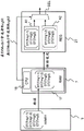
Fig. 2 illustrates a drive control device 4 applied to a portable information terminal device such as a tablet personal computer and a smartphone, which is an example of an electronic apparatus. In the portable information terminal device SYSTM, a panel module (PNL) including a display panel (LCD) 2 such as a dot matrix type liquid crystal display panel and a Touch Panel (TP) 3 capable of touch detection using a mutual capacitance method or a self-capacitance method is disposed on a surface of a housing.
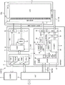
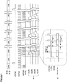
The panel module PNL is configured by a so-called In-Cell system In which, for example, as illustrated In fig. 3, a display panel 2 In which a plurality of display elements PXL are arranged In a matrix and a touch detection electrode ECR constituting a detection capacitance Ctp are integrally assembled with a touch panel 3 arranged In a matrix at a density lower than that of the display elements PXL. The In-Cell system has a TFT array substrate In which TFTs and pixel electrodes constituting the display elements PXL are arranged In a matrix on a glass substrate, for example, and is configured by stacking thereon a liquid crystal layer, a common electrode layer for the pixel electrodes, a color filter, touch detection electrodes constituting detection capacitors, a surface glass, and the like. In fig. 3, the display panel 10 and the touch panel 11 are illustrated as being separated from each other in the left-right direction for convenience, but actually overlap each other.
Although not particularly limited, according to fig. 3, the display panel 2 is provided with a thin film transistor Tr called a TFT disposed at each intersection of scanning electrodes G1 to G1000 and signal electrodes S1 to Sk (k is a positive integer) which are gate lines disposed to intersect each other, scanning electrodes G1 to G1000 corresponding to the gate of the thin film transistor Tr and signal electrodes S1 to Sk corresponding to the source of the thin film transistor Tr are provided, and a liquid crystal element and a storage capacitor (in the figure, the liquid crystal element and the storage capacitor are represented by 1 capacitor Cpx) which are subpixels are formed between the drain of the thin film transistor Tr and a common electrode VCOM. The row of pixels along each of scan electrodes G1-G1000 is referred to as a scan line or a display line. In the display control, the scanning electrodes G1 to G1000 are sequentially driven, and the thin film transistor Tr is turned on for each scanning electrode, whereby a current flows between the source and the drain, and at this time, the respective signal voltages (gradation voltages) applied to the source via the signal electrodes S1 to Sk are applied to the liquid crystal element Cpx, whereby the state of the liquid crystal is controlled. The panel module PNL includes a scanning circuit 1 that sequentially drives the scanning electrodes G1 to G1000.
In fig. 3, the touch panel 3 is not particularly limited, but the touch detection electrodes ECR are arranged in a matrix corresponding to a self-capacitance system in the capacitance type. The touch detection electrodes ECR are individually connected to the touch detection signal lines TRX1 to TRX20, and the opposite poles of the touch detection electrodes ECR form a floating capacitance and are commonly connected to the ground terminal GND of the circuit. Although not particularly limited, in fig. 3, the common electrode VCOM is divided into 20 parts in units of 50 display lines, and each of the divided common electrodes VCOM is shared with the corresponding touch detection signal lines TRX1 to TRX20, thereby reducing the thickness of the panel module PNL. For example, the floating capacitance of the touch detection electrode ECR is charged via the touch detection signal lines TRX1 to TRX 20. If a finger is present nearby, the floating capacitance increases. The charged electric charges are redistributed between the reference capacitance of the touch detection circuit, and the presence or absence of a touch can be detected based on the length of the discharge time of the redistributed electric charges. By using the touch panel 3 overlapping the display panel 2, when a touch operation is performed on the touch panel 3 in accordance with the screen display of the display panel 2, the operation can be discriminated from the touch coordinates obtained by the touch operation.
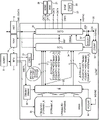
In fig. 2, the drive control device 4 includes a display controller (LCDD) 8 as a display control unit for performing display control of the display panel 2, a touch controller (TPC) 6 as a touch control unit for performing touch detection control of the touch panel 3, and a Microprocessor (MPU) 7 as an arithmetic control unit for performing arithmetic control. The display controller 8 and the microprocessor 7 interface with the host device (HST) 5. The host device 5 is configured by a communication circuit for mobile communication, proximity communication, or the like, and various peripheral devices, for example, centering on a host computer. The drive control device 4 is not particularly limited, but is formed on 1 semiconductor substrate such as single crystal silicon by a known CMOS integrated circuit manufacturing technique and is implemented as a monolithic semiconductor integrated circuit. Or may be implemented as a multi-chip semiconductor module product or the like.
The touch panel controller 6 includes, for example: a detection voltage output circuit (TxD) 10 for sequentially selecting the touch detection signal lines TRX1 to TRX20 to charge the floating capacitance of the touch detection electrode ECR thereof; a detection circuit (RxD) 11 that receives the charge of the touch detection electrode ECR from the selected touch detection signal line, redistributes the charge with the reference capacitance, and detects a discharge time of the redistributed charge; a RAM13 for temporarily storing data of the detection time; and a touch control circuit (TCNT) 14. The touch control circuit 14 controls selection of the touch detection signal lines TRX1 to TRX20 and output timing of the detection voltage by the detection voltage output circuit 10, and controls operation timing of the detection circuit 11 and write operation of the RAM13 in synchronization with the selection. When the detection data of the discharge time of the touch detection electrode ECR over the entire surface of the touch panel 3 is stored in the RAM13, the touch control circuit 14 sends the detection data to the microprocessor 7. The microprocessor 7 determines the presence or absence of touch based on the detection data, calculates position coordinates of the touch position on the touch panel 2, and supplies the result to the host device 5. Regarding the touch detection operation using the detection voltage output circuit 10 and the detection circuit 11 by the touch control circuit 14, the touch control circuit 14 can perform the touch detection operation when the state signal DST output from the display controller 8 allows the touch detection operation during the non-display driving period.
The microprocessor 7 is not particularly limited, but a Central Processing Unit (CPU) 18 sequentially executes programs stored in a rewritable nonvolatile memory (PROM) 16 to perform data processing. The RAM17 is a work area of the CPU18, and is a timing counter (TMR) 15 and the like representatively shown as peripheral circuits of the CPU 18.
In fig. 2, the display controller 8 includes, for example, a scanning line Selection Circuit (SCND) 20, a signal line drive circuit (SIGD) 21, a FIFO memory (FIFO memory) 22 accessed in a first-in first-out format, a line latch circuit (LTCH) 23, a power supply circuit (PWR) 24, a main interface circuit (SYSIF) 25, and a display control circuit (LCNT) 26 as a control circuit for controlling the entire display controller 8, and performs display control of the display panel 2 and instruction of a touch detection operation for the touch controller 6 in synchronization with an internal synchronization signal.
Fig. 2 illustrates the reference clock signal SCK, the display line clock signal LCK, the internal frame synchronization signal IVSYNC, and the internal horizontal synchronization signal IHSYNC as the internal synchronization signals. The main interface circuit 25 inputs display data from the host device 5 in synchronization with the frame synchronization signal VSYNC and the horizontal synchronization signal HSYNC, outputs the internal frame synchronization signal IVSYNC in synchronization with the period of the frame synchronization signal, and also outputs the reference clock signal SCK which is the oscillation clock signal of the clock generator 28 and the display line clock signal CK obtained by dividing the frequency thereof. The clock generator 28 always performs an oscillation operation by the power-on reset of the drive control device 4, and accordingly, the reference clock signal SCK and the display line clock signal CK also always perform clock change. The internal frame synchronization signal IVSYNC specifies a display frame period in the internal operation of the display controller 8. The internal frame synchronization signal IVSYNC has a period corresponding to a display frame period, and although not particularly limited, has a frequency of 60Hz, and 1 period is 16 msec. The frequency of the reference clock signal SCK is fixed. The display line clock signal LCK is a clock signal synchronized with the period of switching the display lines, and is at the position of the reference clock signal for display operation. The display line clock signal LCK has a frequency higher than the frequency of the horizontal synchronization signal HSYNC supplied from the outside of the drive control device 4, and details will be described later, but this frequency can be variable, that is, the frequency division ratio with respect to the reference clock signal SCK is variable. The internal horizontal synchronization signal IHSYNC is outputted from the display control circuit 26 together with other control signals, is a clock signal that changes in synchronization with the period of switching display lines during driving the display lines, and has the same frequency as the display line clock signal LCK.
The host interface circuit 25 receives a display command and display data from the host device 5. The received display data is sequentially stored in the FIFO memory 22 so as to absorb the difference between the supply rate of the display data and the display operation speed, and sequentially read out so as to catch up with the display timing, and transferred to the row latch circuit 23. The signal line drive circuit 21 outputs the gradation voltages in parallel to the plurality of signal electrodes of the display panel 2 in accordance with the display data latched in the row latch circuit 23. Here, the FIFO memory 22 does not have a storage capacitance capable of storing display data for 1 frame. The writing of display data into the FIFO memory 22 is performed in synchronization with the frame synchronization signal VSYNC and the horizontal synchronization signal HSYNC, and the reading is performed in synchronization with the display line clock signal LCK.
The scanning line selection circuit 20 outputs, for example, scanning line selection clock signals GCK1 to GCK4 and shift data Dsft to the scanning circuit 1 of the panel module PNL in order to sequentially select the scanning lines of the display elements, that is, the scanning electrodes G1 to G1000. The scan circuit 1 is not particularly limited, but includes a shift register for shifting the shift data Dsft from the first stage to the final stage in accordance with changes in the scan line selection clock signals GCK1 to GCK 4. The shift register includes 1000 stages of latch stages corresponding to the number of scan electrodes G1 to G1000, each of the latch stages is composed of a master-slave latch circuit, and each of the master-slave latch circuits receives the scan line selection clock signals GCK1 to GCK4 to perform a master-slave latch operation, and determines an output of the latch stage in synchronization with a change in the scan line selection clock signal GCK 4. That is, each latch stage sends latch data to the next stage for a predetermined period in synchronization with a change in the scan line selection clock signal GCK 4. The output of each latch stage is input to a gate driver, and the gate driver drives the corresponding scan electrode to a selection level with an output corresponding to the shift data Dsft. Thus, the thin film transistor is turned on in units of scanning electrodes, and at this time, the signal line driver circuit 21 applies a signal voltage to the display element via the signal electrodes S1 to Sk for each horizontal scanning period based on the display data latched in the row latch circuit 23. Therefore, the display element is display-driven in units of display lines in synchronization with the scanning drive of the scanning electrode in units of frame periods. The signal voltage (gradation voltage) and the like output from the signal line drive circuit 21 are generated by the power supply circuit 24.
The display control circuit 26 performs the above-described display control and the overall control of the display controller 8 such as an instruction to the touch controller 6 based on a display command supplied from the host device 5, control data set in the registers 27 and 28, and the like. CNT1 is a control signal for the scan line selection circuit 20, CNT2 is a drive control signal for the signal line drive circuit 21, CNT3 is a latch control signal for the row latch circuit 23, CNT4 is an access control signal for the FIFO memory 22, and CNT5 is an input/output control signal for the main interface circuit 25 and a frequency control signal for the clock pulse generator 28.
First frame mode and second frame mode
The display control circuit 26 further generates the non-display driving period LHB and the display driving period DISP in a period sandwiched by a blank period of both the first and last of the display frame period FLM, for example, the leading and trailing porches BCKP and FRNTP and the blank BLNK as illustrated in fig. 4. The display frame period FLM means a period of 1 cycle of the internal frame synchronization signal IVSYNC. The generation modes of the non-display driving period LHB and the display driving period DISP are set to two modes, i.e., a first frame mode FMode1 and a second frame mode FMode 2. The first frame mode FMode1 is an operation mode as follows: a non-display driving period LHB and a display driving period DISP are alternately generated a plurality of times in a period sandwiched between two blank periods at the head and the tail of a display frame period FLM, touch detection control is instructed to a touch control section in the non-display driving period, and display control is performed for each display driving period. As is apparent from the drawing, in the first frame mode FMode1, since the display frame period FLM is allocated to the plurality of non-display driving periods LHB, the frequencies of the internal horizontal synchronization signal IHSYNC and the display line clock signal LCK are higher than the frequency of the external horizontal synchronization signal HSYNC, as compared with the case of the second frame mode. Therefore, when the display data is written into the FIFO memory 22 in synchronization with the external horizontal synchronizing signal HSYNC (see fig. 13), the FIFO memory 22 must be read out at a speed faster than the writing speed in the first frame mode FMode1 (see fig. 14).
The second frame mode FMode2 is an operation mode as follows: a non-display driving period LHB and one display driving period DISP subsequent thereto are generated in a period sandwiched between two blank periods at the head and the tail of a display frame period FLM, and a touch detection control is not instructed to a touch control section in the non-display driving period, and a display control is performed in the display driving period. In the second frame mode FMode2, the frequency of the internal horizontal synchronization signal IHSYNC and the frequency of the display line clock signal LCK need only be slightly higher than the frequency of the external horizontal synchronization signal HSYNC, because the non-display driving period LHB is a minute period in the display frame period FLM. Therefore, when the display data is written into the FIFO memory 22 in synchronization with the external horizontal synchronization signal HSYNC (see fig. 13), the FIFO memory 22 can be read out at a speed slightly higher than the writing speed in the second frame mode FMode2 (see fig. 15).
Frequency of display line clock signal LCK is different according to frame mode
The display control circuit 26 controls the frequency of the display line clock signal LCK according to the frame mode. That is, the display control circuit 26 outputs the display line clock signal LCK of the first period Tmg1-1 (see fig. 16) to the clock pulse generator 28 in the first frame mode FMode1, and outputs the display line clock signal LCK of the second period Tmg1-2 (see fig. 17) longer than the first period Tmg1-1 in the second frame mode. The frequency control of the internal horizontal synchronization signal IHSYNC and the display line clock signal LCK is not particularly limited, but can be realized by controlling the frequency division ratio with respect to the reference clock signal SCK.
As described above, the scanning line driving circuit 20 changes the scanning line selection clock signals GCK1 to GCK4 in pulses in synchronization with the display line clock signal LCK, and the signal line driving circuit 21 changes the display driving signals S1 to Sk in synchronization with the display line clock signal LCK. That is, the output timing of the signal voltage to the signal electrodes S1 to Sk and the change timing of the scan line selection clock signals GCK1 to GCK4 are each synchronized with the clock change of the display line clock signal LCK. At this time, the scan line driving circuit 20 generates the scan line selection clock signal GCK4 so that the first intervals (Tmg 2 to Tmg 3) from the timing of switching the outputs of the display driving signals S1 to Sk to the pulse change of the scan line non-selection of the scan line selection clock signal GCK4 become equal in both the case where the cycle of displaying the line clock signal LCK is the first cycle Tmg1-1 as illustrated in fig. 16 and the case where the cycle is the second cycle Tmg1-2 as illustrated in fig. 17. Specifically, as illustrated in fig. 16 and 17, the first interval is defined as a difference between the third interval Tmg3 and the second interval Tmg 2. That is, in the scanning line driving circuit 20, the scanning line selection clock signal GCK4 is changed in a pulse (falling change) for non-selection of a scanning line at a timing when the second interval Tmg2 has elapsed since the start of the pulse change of the display line clock signal LCK. In the signal line drive circuit 21, the output of the display drive signal is switched at the timing when the third interval Tmg3 has elapsed since the start of the pulse change of the display line clock signal LCK. The second interval Tmg2 and the third interval Tmg3 can be controlled as the time from the start of the change of the rising pulse of the display line clock signal LCK to the start of counting the number of changes of the reference clock signal SCK and the time until the count value reaches a predetermined value.
In which of the first frame mode and the second frame mode, that is, even if the clock cycle of the display line clock signal LCK differs depending on the type of the frame mode, the driving time of the display element by the display driving signal switched in synchronization with the change of the display line clock signal is fixed at the first interval. If the driving time of the display element changes according to the frame mode, even if the same signal voltage is used, the amount of charge of the electric charge accumulated in the display element varies, and display unevenness such as color unevenness occurs. Therefore, even if the clock period of the display line clock signal is different depending on the type of the frame mode, there is no risk of display unevenness occurring.
The start timing of the display period differs between display frames in the first frame mode
In the first frame mode FMode1, the start timing of the display driving period DISP and the start timing of the non-display driving period LHB subsequent thereto are changed in units of display frame periods for each of the plurality of display frame periods. In the second frame mode FMode2, the display driving period DISP is not divided by the non-display driving period LHB in the display frame period FLM or the start timings of the non-display driving period LHB and the display driving period DISP in the display frame period FLM are not changed for each display frame period.
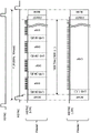
The following is illustrated in fig. 5: in the first frame mode FMode1, the start timing of the display driving period DISP and the start timing of the non-display driving period LHB are changed in units of a plurality of (n) display frame periods for each of the display frame periods. FMode1_0 indicates the difference in the start timings by indicating the division of the arrangement of the non-display driving period LHB and the display driving period DISP in the first display frame period by the clock number Tline of the display line clock LCK. The subscripts attached to the display driving period DISP and the non-display driving period LHB mean the order of arrangement of the periods, "display" means performing a display operation, and "touch" means performing a touch detection operation. Here, the clock number Tline of the display driving period DISP is substantially 100, and the display operation is performed during this period, and the clock number Tline of the non-display driving period LHB is 50, and the touch detection operation is performed during this period. The next display frame period is denoted by FMode1_ 1. The difference from FMode1_0 is that: the clock number Tline of the first display driving period DISP-1 is increased to 100+ i and the clock number Tline of the last display driving period DISP-10 is decreased to 100-i. The (n + 1) th last display frame period is denoted by FMode1_ n. The difference from FMode1_0 is that: the clock number Tline of the first display driving period DISP-1 is increased to 100+ N (N = i × N), and the clock number Tline of the last display driving period DISP-10 is decreased to 100-N. In this way, in the operation modes FMode1_0 to FMode1_ n for each display frame period in the first frame mode FMode1, the start timings of the display driving period DISP and the non-display driving period LHB are shifted by the clock number i (Tline) one by one, and in each mode, the display driving period DISP is 10 times, the non-display driving period LHB is 9 times, and the last timing of each operation mode is held at 1500 Tline which is fixed. Although not particularly limited, the touch detection operation using the non-display driving period LHB is performed in such a manner that the entire surface of the touch panel 3 is scanned 1 time in each of the operation modes FMode1_0 to FMode1_ n in the first frame mode FMode 1. Therefore, touch determination such as touch coordinate calculation based on the entire-surface scanning detection operation of the touch panel can be performed for 16msec per display frame period. The characters i and n each mean an appropriate integer, and i × n is preferably smaller than the number of display lines in one display driving period DISP.
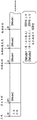
Fig. 6 illustrates the configuration of the display driving period DISP and the non-display driving period LHB of the display frame period FLM in the second frame mode FMode 2. Similarly to fig. 5, the division of the display driving period DISP and the non-display driving period LHB is represented by the clock number Tline of the display line clock LCK. "display" means performing a display operation, and "none" means suppressing a touch detection operation. Here, the clock number Tline of the display driving period DISP is 1450, during which the display operation is performed, and the clock number Tline of the non-display driving period LHB is 50, during which the touch detection operation is not performed.
As is apparent from fig. 5, in the first frame mode FMode1, the boundary position of the display driving period DISP and the non-display driving period LHB changes in each of the plurality of display frame periods FLM, and therefore, flicker can be prevented in the display screen. The second frame mode FMode2 has one display driving period DISP, and the display driving period DISP is not divided by a non-display driving period in the middle of the display driving period, and therefore, flicker is not originally generated in the display screen during the display period. Further, control in consideration of the fact that the start timing of the display driving period in the second frame mode FMode2 does not coincide with the start timing of the display driving period in the first frame mode FMode1 which changes sequentially between a plurality of display frames is not necessary at all, and therefore, control of the frame mode as a whole is simplified.
First display mode and second display mode
As is clear from the description of fig. 5 and 6, in the first frame mode FMode1, the DISP performs the display operation during the display driving period and the LHB performs the touch detection operation during the non-display driving period. In contrast, in the second frame mode FMode2, the DISP performs the display operation during the display driving period, but the LHB does not perform the touch detection operation during the non-display driving period. Therefore, in the case where the touch detection frequency is low, in the aspect of using only the second frame mode for low power consumption, it is not possible to determine whether or not a new touch is present in order to return to the first frame mode FMode1, and therefore, in this case, it is necessary to mix the second frame mode in the first frame mode at a ratio of 1 time out of the multiple frame periods. Accordingly, the microprocessor 7 changes the use method of the control data of the first frame mode FMode1 and the control data of the second frame mode FMode2 in the display control circuit 26 based on the touch detection result of the touch controller 6. The manner of the method of using the control data of the first frame mode FMode1 and the control data of the second frame mode FMode2 is not particularly limited, but is two types of the first display mode DMode1 and the second display mode DMode 2.
Fig. 9 illustrates the use modes of the frame modes FMode1 and FMode2 when the first display mode DMode1 is designated. The first display mode DMode1 is an operation mode in which the first frame mode FMode1 is continuous in units of a plurality of display frame periods FLM. In the example of fig. 9, the first frame patterns in units of n = 23 operation modes FMode1_0, FMode1_1, and FMode1_2 in fig. 5 are made continuous. In the first display mode DMode1, the DISP performs a display operation during the display driving period and the LHB repeats a touch detection operation during the non-display driving period for each frame. That is, touch determination such as touch coordinate calculation based on touch detection can be performed for each display frame period at intervals of 16 msec.
Fig. 8 illustrates a manner of using the frame mode when the second display mode DMode2 is designated. The second display mode DMode2 is an operation mode in which the following operations are repeated: the second frame mode FMode2 in units of the plurality of display frame periods FLM is performed during a part of the display frames thereof, and the first frame mode FMode1 is performed during one display frame thereof during the last display frame. In the example of fig. 8, the second frame mode corresponding to the two operation modes FMode2_0 and FMode2_1 in fig. 6 and the first frame mode corresponding to the last operation mode FMode1_2 when n =2 in fig. 5 are repeated as a unit. In the second display mode DMode2, a touch detection operation is performed in which the non-display drive period LHB is used at a rate of 1 display frame period in the 3-display frame period FLM. That is, touch determination such as touch coordinate calculation by touch detection is performed at 48msec intervals, which is a display frame period corresponding to 3 frames. Accordingly, it is ensured that the second display mode DMode2 with low power consumption can be restored to the first display mode DMode1 as needed.
Concrete control modes of display mode and frame mode
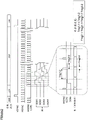
Fig. 1 shows an example of the display control circuit 26 that supports the first display mode and the second display mode. The display control circuit 26 has a Frame Counter (FCOUNT) 30, a line counter (lcoount) 31, an interval counter (icoount) 37, a start timing register 32, first control logic (SEL) 33, second control logic (TLog) 34, third Control Logic (CLOG) 35, a display mode register 36, and a clock control register 27.
The start timing register 32 is provided with a plurality of settings DT (FMode 1_ 0) to DT (FMode 1_ n) as fifth control data of the first frame mode FMode1 and sixth control data DT (FMode 2) as control data of the second frame mode FMode2 so as to be rewritable. The plurality of settings DT (FMode 1_ 0) to DT (FMode 1_ n) of the fifth control data and the sixth control data DT (FMode 2) are held in the nonvolatile memory 9 in the system, and the microprocessor 7 initially sets the plurality of settings DT (FMode 1_ 0) to DT (FMode 1_ n) of the fifth control data and the sixth control data DT (FMode 2) in the start timing register 32 from the nonvolatile memory 9 by a process of system reset or power-on reset.
The clock control register 27 is provided with first control data DT (Tmg 1-1) specifying the first cycle Tmg1-1, second control data DT (Tmg 1-2) specifying the second cycle Tmg1-2, third control data DT (Tmg 2) specifying the second interval Tmg2, and fourth control data DT (Tmg 3) specifying the third interval Tmg3 so as to be rewritable. The first to fourth control data DT (Tmg 1-1), DT (Tmg 1-2), DT (Tmg 2), and DT (Tmg 3) are retained by the nonvolatile memory 9 on the system, and the microprocessor 7 initially sets the first to fourth control data DT (Tmg 1-1), DT (Tmg 1-2), DT (Tmg 2), and DT (Tmg 3) in the start timing register 32 from the nonvolatile memory 9 by a process of system reset or power-on reset.
The first control data DT (Tmg 1-1) and the second control data DT (Tmg 1-2) are not particularly limited, but are frequency division number data of the reference clock signal SCK. The third control data DT (Tmg 2) and the fourth control data DT (Tmg 3) each specifying an interval are not particularly limited, but are count value data to be compared with the count value of the reference clock signal of the interval counter 37.
The fifth control data DT (FMode 1_ 0) -DT (FMode 1_ n) are data for defining operation modes of FMode1_ 0-FMode 1_ n at start timings of a display drive period DISP and a non-display drive period LHB in units of display frame periods among a plurality of display frame periods in correspondence with the first frame mode FMode1, and as described in fig. 5, have data for each of a period number, a difference in display operation ("display")/touch detection ("touch"), and a clock number of a period indicated by Tline, of each of the display drive periods and the non-display drive period LHB in each of the operation modes FMode1_ 0-FMode 1_ n.
The sixth control data DT (FMode 2) is data for specifying the start timing of the display driving period DISP in units of display frame periods among a plurality of display frame periods in accordance with the second frame mode FMode2, and has data indicating each of the period number of the display driving period, the difference between display operation ("display")/touch detection suppression ("no"), and the number of clocks of the period indicated by Tline in the operation mode FMode2, as described with reference to fig. 6.
In the mode register 36, the microprocessor 7 is provided with display mode data of the first display mode DMode1 or the second display mode DMode2 in a changeable manner using the mode setting signal MSET. The operation using the setting mode data of the microprocessor 7 is performed based on the control flow illustrated in fig. 10. That is, after power-on (S1), the second display mode DMode2 is first set, and determination is made as to whether or not a touch operation has been performed at a frequency specified by the mode, and the display mode is continued until the touch operation is determined (S2). When the touch operation is determined, the display mode is changed to the first display mode DMode1, and whether or not the touch operation is performed is determined by the touch detection operation for each display frame (S3). The microprocessor 7 starts the timer counter 15 in response to a change to the first display mode, resets the timer counter 15 when a touch operation is determined before a fixed period of time-out elapses, and resumes the timer operation from the beginning, and changes the display mode to the second display mode DMode2 in response to a time-out of the timer counter 15 when a touch operation cannot be determined before the fixed period elapses. The same control operation is repeated below. The workflow realized by the above control flow is, for example, as shown in fig. 7.
The first control logic 33 selects data of a desired setting from among the settings of the fifth control data DT (FMode 1_ 0) to DT (FMode 1_ n) and the second control data DT (FMode 2) for each display frame period in accordance with the display mode set in the mode register 36 and the count value of the frame counter 30. For example, to facilitate understanding, n =2 is set in accordance with the examples of fig. 8 and 9, and the frame counter 30 counts the internal frame synchronization signal IVSYNC so as to wrap around from the initial value 0 to 2. In this case, in the first display mode DMode1, the first control logic 33 selects the control data DT (FMode 1_ 0) of the first frame mode FMode1 when FCOUNT =0, selects the control data DT (FMode 1_ 1) of the first frame mode FMode1 when FCOUNT =1, and selects the control data DT (FMode 1_ 2) of the first frame mode FMode1 when FCOUNT = 2. This selection corresponds to fig. 9. In the second display mode DMode2, the first control logic 33 selects the control data DT (FMode 2_ 0) of the second frame mode FMode2 when FCOUNT =0, selects the control data DT (FMode 2_ 1) of the second frame mode FMode2 when FCOUNT =1, and selects the control data DT (FMode 2_ 2) of the second frame mode FMode2 when FCOUNT = 2. This selection corresponds to fig. 8.
The second control logic 34 sequentially generates the state signal DST at the start timing of each of the display drive period DISP and the non-display drive period LHB defined in the display frame period in accordance with the count value of the line counter 31 in each display frame period based on the count value reaching the control data selected by the first control logic 33. The line counter 31 counts the display line clock signal LCK, and the count value is reset for each display frame period by the internal frame synchronization signal IVSYNC. The logic for generating the state signal DST of the second control logic 34 is as described in fig. 11 with respect to the control data selected in the first display mode DMode 1. The logic for generating the state signal DST of the control logic 34 for the control data selected in the second display mode DMode2 is shown in fig. 12, for example. Although not particularly limited, the code d0d1 whose DST is 2 bits, d0 indicate the display operation with H (e.g., logical value 1), suppress the display operation with L (e.g., logical value 0), d1 indicate the touch detection operation with H, and suppress the touch detection operation with L. Further, the second control logic outputs a mode decision signal DISmd indicating whether the control of the first frame mode FMode1 is currently performed or the control of the second frame mode FMode2 is currently performed according to the control data selected by the first control logic 33.
The generation logic illustrated in fig. 11 corresponds to fig. 9, and the display drive period DISP performing the display operation and the non-display drive period LHB performing the touch detection operation are alternately generated in each display frame period FLM. That is, in such a case that the frequency of performing the touch operation is high, the display operation and the touch detection operation are exclusively performed for each display frame period by the first display mode DMode 1.
The generation logic illustrated in fig. 12 corresponds to fig. 8, and in the first 2 of every three display frame periods, the display drive period DISP in which the display operation is performed and the non-display drive period LHB in which the touch detection operation is suppressed are alternately generated in each display frame period FLM, and the display drive period DISP in which the display operation is performed and the non-display drive period LHB in which the touch detection operation is performed are alternately generated in the last display frame period FLM. In such a case that the frequency of performing touch operations is high, the display operation and the touch detection operation are exclusively performed for each display frame period. That is, in such a case that the frequency of performing the touch operation is low, the display operation and the touch detection operation are exclusively performed only in the display frame period at the end of each of the plurality of display frame periods in the second display mode DMode 2.
The third control logic 35 supplies the command CMD and the command parameter CDATA from the host device 5 together with the state signal DST and the mode discrimination signal DISmd, and further supplies the count value of the interval counter 37. The interval counter 37 counts the reference clock signal SCK for each period of the display line clock signal LCK. The count value is a value that is plotted in a plurality of steps within a period in which the line clock signal LCK is to be displayed. The third control logic 35 generates the control signals CNT1, CNT2, CNT3, CNT4, CNT5, and the internal horizontal synchronization signal IHSYNC using the count value of the interval counter 37, the state signal DST, the mode discrimination signal DISmd, the decoding result of the command CMD, and the command parameter CDATA. The control signals CNT1, CNT2, CNT3, CNT4, and CNT5 are generated in synchronization with the reference clock signal SCK, the display line clock signal LCK, and the internal frame synchronization signal IVSYNC according to their control functions.
The third control logic inputs the control data DT (Tmg 1-1) and DT (Tmg 1-2) set in the clock control register 27, recognizes which of the first frame pattern FMode1 and the second frame pattern FMode2 the current operation mode is based on the value of the mode discrimination signal discd, supplies the clock pulse generator 28 with a frequency control signal for controlling the display line clock signal LCK to the frequency of the cycle indicated by the control data DT (Tmg 1-1) when the mode discrimination signal discd indicates the first frame pattern, and supplies the clock pulse generator 28 with a frequency control signal for controlling the display line clock signal LCK to the frequency of the cycle indicated by the control data DT (Tmg 1-2) when the mode discrimination signal discd indicates the second frame pattern. The frequency control signal is contained in the control signal CNT 5. In this example, the control data is frequency division data for the reference clock signal SCK, thereby defining the clock frequency.
The third control logic 35 inputs the control data DT (Tmg 2) and DT (Tmg 3) set in the clock control register 27, and supplies the signal line drive circuit 21 with a timing signal in which the count value of the interval counter 37 matches the value of the control data DT (Tmg 3). Thus, the signal line drive circuit 21 switches the output of the signal voltage from the rise of the display row clock signal LCK through the interval Tmg3 as illustrated in fig. 16 and 17. The timing signal is contained in the control signal CNT 2.
Further, the third control logic 35 supplies a timing signal in which the count value of the interval counter 37 coincides with the value of the control data DT (Tmg 2) to the scan line selection circuit 20. The scanning line selection circuit 20 sequentially generates and outputs 4-phase scanning line selection clock signals GCK1 to GCK4 at a predetermined pulse width in synchronization with the display line clock signal LCK. For example, as illustrated in fig. 16 and 17, each of the scan line selection clock signals GCK1 to GCK4 rises sequentially with a delay of 1 cycle of the display line clock signal LCK, and falls at a timing at which the interval Tmg2 indicated by the timing signal has elapsed from the rise of the third cycle of the display line clock signal when falling in the third cycle of the display line clock signal LCK. The timing signal is contained in the control signal CNT 1.
The third control logic 35 controls driving of a new scan electrode by the scan line drive circuit 20, driving of a signal electrode by the signal line drive circuit 21, and a latch operation of new display data by the row latch circuit 23, in a period d0= H in which the state signal DST indicates the display drive period. Further, the control circuit 14 of the touch panel controller 6 to which the state signal DST is supplied performs the touch detection operation for the touch frame with d1= H during the non-display driving period in which the state signal DST is set to the state signal DST. In a period in which the state signal DST is d0= L in the non-display driving period, the third control logic 35 stops the driving of the new scan electrode by the scan line driving circuit 20, the driving of the signal electrode by the signal line driving circuit 21, the latch operation of the new display data by the row latch circuit 23, and the like, and stops the display operation in this period. Further, the control circuit 14 of the touch panel controller 6 to which the state signal DST is supplied performs the touch detection operation for the touch frame with d1= H in the non-display period of the state signal DST, and suppresses the touch detection operation for the touch frame with d1= L.
Although the access control of the FIFO memory 22 is performed such that the FIFO memory 22 is not emptied of data during the display driving period DISP, the display data transfer rate from the host device 5 is slower than the display speed, and therefore, in order to ensure that the FIFO memory 22 is not emptied of data during the display driving period DISP, the writing operation of the display data into the FIFO memory 22 is performed also during the non-display driving period LHB. In order to ensure that the FIFO memory 22 does not become empty in the display driving period DISP, the first period Tmg1-1 is a period for ensuring that the FIFO memory 22 in which display data is written in the display frame period in the first frame mode FMode1 does not become empty due to an intermittent and faster-than-writing reading operation in the display driving period. The second period Tmg1-2 is a period for ensuring that the FIFO memory 22 in which display data is written in the display frame period in the second frame mode FMode2 does not become empty due to a continuous read operation at a speed faster than the write operation in the display driving period DISP.
The first to third control logics 33, 34, 35 may be hard-wired logics or may be program processing circuits whose logical operations are determined by a software program such as firmware. The former wins out in terms of high speed of processing, and the latter wins out in terms of versatility or flexible correspondence.
Fig. 18 illustrates a method of setting the control data DT (Tmg 1-1), DT (Tmg 1-2), DT (Tmg 2), and DT (Tmg 3) in the clock control register 27. At the time of power-on reset or system reset, the CPU transfers control data DT (Tmg 1-1), DT (Tmg 1-2), DT (Tmg 2) and DT (Tmg 3) from the nonvolatile memory device 89 to the RAM17, initially sets DT (Tmg 2) and DT (Tmg 3) in the memory areas a2 and A3 of the clock control register 27, sets control data DT (Tmg 1-1) in the area a1 in accordance with the designation of the first display mode DMode1, and sets control data DT (Tmg 1-2) in the area a1 in accordance with the designation of the second display mode DMode 2. Alternatively, as shown in fig. 19, the initial setting of the control data DT (Tmg 1-1), DT (Tmg 1-2), DT (Tmg 2) and DT (Tmg 3) to the memory areas a1, a2, A3 and a4 of the clock control register 27 is completed at the time of reset, the control data DT (Tmg 1-1) of the area a1 may be selected by the selector SEL in accordance with the designation of the first display mode DMode1, and the control data DT (Tmg 1-2) of the area a2 may be selected in accordance with the designation of the second display mode DMode 2. Further, as shown in fig. 20, control data DT (Tmg 1-1), DT (Tmg 2) and DT (Tmg 3) used in the first display mode DMode1 may be initially set in the storage area a1 of the clock control register 27, control data DT (Tmg 1-2), DT (Tmg 2) and DT (Tmg 3) used in the second display mode DMode2 may be initially set in the storage area a2 of the clock control register 27, and control data DT (Tmg 1-1), DT (Tmg 2) and DT (Tmg 3) of the area a1 may be selected by the selector SEL according to the designation of the first display mode DMode1, and control data DT (Tmg 1-2), DT (Tmg 2) and DT (Tmg 3) of the area a2 may be selected according to the designation of the second display mode DMode 2.
According to the drive control device 4 described above, the following operational effects are provided.
(1) In the first frame mode FMode1, the start timing of the display driving period DISP and the start timing of the non-display driving period LHB are changed in units of the display frame period FLM, and therefore, it is possible to suppress an undesirable luminance difference due to non-display from being seen at a fixed position in the display frame FLM or a phenomenon of flicker due to the difference. The second frame mode FMode2 has one display driving period DISP, and the display driving period DISP is not divided by a non-display driving period in the middle of the display driving period, and therefore, flicker is not originally generated in the display screen during the display period. Further, since there is no need to perform control in consideration of the fact that the start timing of the display driving period in the second frame mode FMode2 does not coincide with the start timing of the display driving period in the first frame mode FMode1 which changes sequentially between a plurality of display frames, the control of the frame mode as a whole is simplified.
(2) Since the method of using or combining the first frame pattern and the second frame pattern is changed as in the first display mode DMode1 and the second display mode DMode2 based on the touch detection result, it becomes easy to deal with the display driving period DISP and the non-display driving period LHB starting at a timing that meets the requirements of the system using the drive control device 4. For example, when a display operation is performed at a speed higher than the transfer rate of display data supplied from the host device when the frame buffer memory is not prepared, even if the touch detection operation is not performed, it is necessary to provide a non-display period for storing display data to be displayed next in the FIFO memory, or to reduce power consumption by lowering the touch detection frequency when a state where no touch detection is performed for a fixed period continues. In response to such a demand, it is easy to change the start timing of the display driving period DISP and the start timing of the non-display driving period LHB in the display frame period FLM depending on the touch detection result.
(3) As described with reference to fig. 5, since the control is performed such that the first display period is gradually increased by a predetermined period and the last display period is shortened by the predetermined period for each display frame period FLM using the control data of the first frame mode FMode1, the control is facilitated such that the start timings of the display drive period DISP and the non-display drive period LHB are different for each display frame period FLM.
(4) By using the first frame mode FMode1 in which the DISP allows the display operation during the display driving and the LHB allows the touch detection operation during the non-display driving, noise generated by the operation of one side does not affect the operation of the other side between the touch detection operation and the display operation.
(5) Since the FIFO memory 22 smaller than the data size of the display frame can be used, it is possible to contribute to downsizing of the drive control device as compared with the case of loading the frame buffer.
The invention made by the present inventors has been specifically described above based on the embodiments, but the invention is not limited thereto, and it goes without saying that various modifications can be made without departing from the scope of the invention.
Another example of the first display mode DMode1 is shown in fig. 21. In fig. 9, the start timings of the display drive period and the non-display drive period are changed for every 1 display frame, but in the present invention, the start timings of the display drive period and the non-display drive period may be changed for every plural display frames, for example, for every two display frames as shown in fig. 23. In this case, for example, the count clock signal of the counter 30 may be a clock signal having a period 2 times that of the internal frame synchronization signal IVSYNC.
Fig. 22 and 23 show another example of the second interval and the third interval. In the case of fig. 16 and 17, when the period for displaying the row clock signal LCK in the first frame mode is the first period Tmg1-1, and when the period for displaying the row clock signal LCK in the second frame mode is the second period Tmg1-2, which is longer than the first period, the second interval Tmg2 and the third interval Tmg3 are set to the same value. The present invention is not limited thereto, and the second interval Tmg2-1 and the third interval Tmg3-1 may be set when the cycle of the row clock signal LCK displayed in the first frame mode FMode1 is the first cycle Tmg1-1 as shown in fig. 22, and the second interval Tmg2-2 and the third interval Tmg3-2 may be set when the cycle of the row clock signal LCK displayed in the second frame mode FMode2 is the second cycle Tmg1-2 as shown in fig. 23. As a precondition thereof, the relationship of "Tmg 2-1" - "Tmg 3-1" = "Tmg 2-2" - "Tmg 3-2" is maintained. At this time, the third control data are DT (Tmg 2-1) and DT (Tmg 2-2), and the fourth control data are DT (Tmg 3) and DT (Tmg 3-2). The operation and effect are the same as those in fig. 16 and 17, but the number of interval setting data increases.
The buffer memory is not limited to the FIFO memory 22, and may be a RAM, or a frame buffer memory made of a RAM.
The manner of shifting the start timing of the display drive period and the non-display drive period in the first frame mode FMode1 is not limited to the method of defining each period by the number of clocks of the horizontal synchronization clock as in fig. 5, and the start timing of each period may be defined by a time or a clock count value or by a mathematical expression, and may be changed as appropriate.
The first non-display driving period LHB in the second frame mode may be a part of the trailing edge, and the boundary with the trailing edge BCKP may not be clear. It is sufficient that the start timing of the next display driving period is clear.
The control logic of the display control unit is not limited to the logic described in fig. 1, 11, 12, and the like, and can be changed as appropriate. The method of using the coefficient value of the reference clock signal for interval control is not limited to the method, and control using other time information and the like may be used. The values of i and j in fig. 5 and 6 may be determined as appropriate. The values of n and m are not limited to 2, and may be determined as appropriate. Of course, the increment value of the frame counter 30 can be variably set.
Further, the display panel to be driven may be an electroluminescence panel or the like. The structure of the display panel as a driving object of the present invention is not limited to fig. 3. The drive control device may be configured by mounting the touch controller 6, the microprocessor 7, and the display controller 8, which are each formed of a different semiconductor chip, on a circuit board. The present invention can be applied not only to portable information terminals such as tablet computers and smart phones, but also to other information terminal devices and the like.
Description of reference numerals
1 Portable information terminal device
2 display panel (LCD)
3 Touch Panel (TP)
4 display control device
5 main device
6 touch controller (TPC) as touch control part
Microprocessor (MPU) as the second control unit
Display controller (LCDD) as display control part 8
10 drive circuit (TxD)
11 detection circuit (RxD)
12 analog-to-digital conversion circuit (ADC)
13 RAM
14 touch control circuit (TCNT)
15 timing counter (TMR)
16 nonvolatile memory (PROM)
18 Central Processing Unit (CPU)
20 scanning line Selection Circuit (SCND)
21 Signal line drive circuit (SIGD)
22 FIFO memory (FIFOMRY)
23 line latch circuit (LTCH)
24 Power supply circuit (PWR)
25 Main interface circuit (SYSIF)
26 display control circuit (LCNT)
27 clock control register
SCK reference clock signal
LCK display line clock signal
IVSYNC internal frame synchronization signal
IHSYNC internal horizontal synchronization signal
CNT1 drive control signal
CNT2 drive control signal
CNT3 latch control signal
CNT4 access control signals
CNT5 input/output control signal
FLM display frame period
DISP display driving period
LHB non-display drive period
BCKP back porch
FRTP front edge
BLNK blanking period
FMode1 first frame mode
FMode2 second frame mode
DT (FMode 1_ 0) -DT (FMode 1_ n) fifth control data
DT (FMode 2) sixth control data
DMmode1 first display mode
DMmode2 second display mode
Tmg1-1 first cycle
Tmg1-2 second cycle
Tmg 2-Tmg 3 first spacing
Tmg2 second spacing
Tmg3 third Interval
DT (Tmg 1-1) first control data
DT (Tmg 1-2) second control data
DT (Tmg 2) third control data
DT (Tmg 3) fourth control data
30 Frame Counter (FCOUNT)
31 Line Counter (LCOUNT)
32 start timing register
33 first control logic (SEL)
34 second control logic (TLOG)
35 third Control Logic (CLOG)
36 mode register
37 Interval Counter (ICOUNT)
DST status signal
Constituent bits of d0, d1 status signals
A disc frame pattern recognition signal.