CN107112172B - Solder sheet, solder, fuse unit, fuse element, protective element, short-circuit element, and switching element - Google Patents
Solder sheet, solder, fuse unit, fuse element, protective element, short-circuit element, and switching element Download PDFInfo
- Publication number
- CN107112172B CN107112172B CN201580059143.2A CN201580059143A CN107112172B CN 107112172 B CN107112172 B CN 107112172B CN 201580059143 A CN201580059143 A CN 201580059143A CN 107112172 B CN107112172 B CN 107112172B
- Authority
- CN
- China
- Prior art keywords
- flux
- conductor
- electrode
- fusible conductor
- sheet
- Prior art date
- Legal status (The legal status is an assumption and is not a legal conclusion. Google has not performed a legal analysis and makes no representation as to the accuracy of the status listed.)
- Active
Links
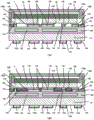
Images


Classifications
-
- H—ELECTRICITY
- H01—ELECTRIC ELEMENTS
- H01H—ELECTRIC SWITCHES; RELAYS; SELECTORS; EMERGENCY PROTECTIVE DEVICES
- H01H37/00—Thermally-actuated switches
- H01H37/74—Switches in which only the opening movement or only the closing movement of a contact is effected by heating or cooling
- H01H37/76—Contact member actuated by melting of fusible material, actuated due to burning of combustible material or due to explosion of explosive material
-
- H—ELECTRICITY
- H01—ELECTRIC ELEMENTS
- H01H—ELECTRIC SWITCHES; RELAYS; SELECTORS; EMERGENCY PROTECTIVE DEVICES
- H01H85/00—Protective devices in which the current flows through a part of fusible material and this current is interrupted by displacement of the fusible material when this current becomes excessive
- H01H85/02—Details
- H01H85/04—Fuses, i.e. expendable parts of the protective device, e.g. cartridges
- H01H85/041—Fuses, i.e. expendable parts of the protective device, e.g. cartridges characterised by the type
- H01H85/044—General constructions or structure of low voltage fuses, i.e. below 1000 V, or of fuses where the applicable voltage is not specified
- H01H85/0445—General constructions or structure of low voltage fuses, i.e. below 1000 V, or of fuses where the applicable voltage is not specified fast or slow type
-
- H—ELECTRICITY
- H01—ELECTRIC ELEMENTS
- H01H—ELECTRIC SWITCHES; RELAYS; SELECTORS; EMERGENCY PROTECTIVE DEVICES
- H01H85/00—Protective devices in which the current flows through a part of fusible material and this current is interrupted by displacement of the fusible material when this current becomes excessive
- H01H85/02—Details
- H01H85/04—Fuses, i.e. expendable parts of the protective device, e.g. cartridges
- H01H85/05—Component parts thereof
- H01H85/165—Casings
Abstract
The flux is appropriately retained in the fusible conductor, while achieving both an improvement in the rating of the fuse element and the like and a quick fusing property. The fuse unit 1 includes a fusible conductor 6 and a solder piece 5 in which solder 7 is impregnated into an insulator, the solder piece 5 is mounted on the fusible conductor 6 and/or under the fusible conductor 6, and the fusible conductor 6 is fused by an overcurrent flowing through the fusible conductor 6. Alternatively, the fuse unit 1 has a fusible conductor 6, and a flux 9 containing an insulator sheet that contains a flowing body or semi-flowing body of the insulator sheet that retains a liquid is coated on the fusible conductor 6 and/or below the fusible conductor 6.
Description
Technical Field
The present invention relates to a fuse unit (fuse element) which is attached to a current path and which interrupts the current path by self-heating when a current exceeding a rated value flows or by heat generation and fusion of a heating element, and particularly relates to a fuse unit having excellent quick-break characteristics, a fuse element, a protective element, a short-circuit element, a switching element, and a flux sheet (flux) and a flux used for them.
The present application claims priority based on japanese patent application No. 2014-229359, filed 11/2014 in japan, which is incorporated herein by reference.
Background
Conventionally, a fuse unit is used which fuses due to self-heating when a current exceeding a rated current flows, and interrupts the current path. As the fuse unit, for example, a clip-fixed fuse in which solder is sealed in a glass tube, a chip fuse in which an Ag electrode is printed on a surface of a ceramic substrate, a screw-fixed fuse in which a part of a copper electrode is thinned and incorporated in a plastic case, an insertion-type fuse, or the like is widely used.
Prior art documents
Patent document
Patent document 1: japanese patent laid-open publication No. 2011-82064.
Disclosure of Invention
Problems to be solved by the invention
However, the conventional fuse unit described above has a problem that surface mounting by reflow is not possible, the current rating is low, and quick-break performance is deteriorated if the rating is increased due to an increase in size.
In the case of a quick-break fuse element for reflow mounting, it is generally preferable that the fuse unit is a high-melting-point solder containing lead and having a melting point of 300 ℃ or higher so as not to be melted by the heat of reflow. However, the use of lead-containing solder is only limitedly recognized in RoHS directive and the like, and it is considered that the demand for lead-free solder will increase in the future.
That is, as the fuse unit, it is required to be capable of surface mounting by reflow and excellent in mountability to the fuse element; the rated value is improved so as to correspond to large current; the fuse has a quick fusing property of quickly cutting off a current path when a rated overcurrent is exceeded.
Accordingly, an object of the present invention is to provide a fuse unit, a fuse element, a protection element, a short-circuit element, and a switching element, which can be surface-mounted and can achieve both of an improvement in rating of the fuse element and a quick fusing property, and a solder pad and a solder used for them.
Means for solving the problems
In order to solve the above-mentioned problems, a solder piece according to the present invention is mounted on a fusible conductor of a fuse element, wherein a solder is impregnated into an insulator, and a specific gravity of the insulator is equal to or less than a specific gravity of the fusible conductor.
The flux according to the present invention is applied to the fusible conductor of the fuse element or to the fusible conductor, and is a fluid or semi-fluid to which an insulator sheet having liquid retentivity is added and which has a specific gravity equal to or lower than that of the fusible conductor.
Further, a fuse unit according to the present invention includes: a fusible conductor; and a flux sheet for dipping the flux into an insulator having a specific gravity equal to or lower than that of the fusible conductor, and mounting the flux sheet on the fusible conductor and/or under the fusible conductor.
Further, a fuse unit according to the present invention includes: a fusible conductor; and adding a flux of a fluid or semi-fluid of an insulator sheet having a specific gravity equal to or lower than that of the fusible conductor and having liquid retentivity, and applying the flux onto and/or under the fusible conductor.
Further, a fuse element according to the present invention includes: a fusible conductor; and a flux piece for dipping the flux into an insulator having a specific gravity equal to or lower than that of the fusible conductor, and mounting the flux piece on the fusible conductor and/or under the fusible conductor, wherein the fusible conductor is fused by an overcurrent flowing through the fusible conductor.
The fuse element according to the present invention includes a fusible conductor, and a flux containing a fluid or semi-fluid of an insulator sheet having a specific gravity equal to or lower than that of the fusible conductor and having liquid retentivity is applied to the fusible conductor and/or below the fusible conductor, and the fusible conductor is fused by an overcurrent flowing through the fusible conductor.
In addition, the protection element according to the present invention includes: an insulating substrate; a heating element formed on or in the insulating substrate; 1 st and 2 nd electrodes formed on the insulating substrate; a 3 rd electrode electrically connected to the heating element; a fusible conductor connected across from the 1 st electrode to the 2 nd electrode via the 3 rd electrode; and a flux piece for dipping the flux into the insulator having a specific gravity equal to or less than that of the soluble conductor, wherein the flux piece is mounted on the soluble conductor and/or under the soluble conductor, and the soluble conductor is fused by heat generated by energization of the heating element, thereby blocking the electrodes between the 1 st and 2 nd electrodes.
In addition, the protection element according to the present invention includes: an insulating substrate; a heating element formed on or in the insulating substrate; 1 st and 2 nd electrodes formed on the insulating substrate; a 3 rd electrode electrically connected to the heating element; and a fusible conductor connected across from the 1 st electrode to the 2 nd electrode via the 3 rd electrode, wherein a flux containing a fluid or semi-fluid of an insulator sheet having a specific gravity equal to or lower than that of the fusible conductor and having liquid retentivity is applied on the fusible conductor and/or below the fusible conductor, and the fusible conductor is fused by heat generated by energization of the heating element to block the gap between the 1 st and 2 nd electrodes.
Further, a short-circuit element according to the present invention includes: an insulating substrate; a heating element formed on or in the insulating substrate; 1 st and 2 nd electrodes formed on the insulating substrate in proximity thereto; a 3 rd electrode electrically connected to the heating element; a fusible conductor connected across from the 1 st electrode to the 3 rd electrode; and a flux piece for dipping flux into the insulator having a specific gravity equal to or less than that of the soluble conductor, wherein the flux piece is mounted on the soluble conductor and/or under the soluble conductor, and the soluble conductor is fused by heat generated by energization of the heating element, thereby performing short-circuiting between the 1 st and 2 nd electrodes and blocking between the 1 st and 3 rd electrodes.
Further, a short-circuit element according to the present invention includes: an insulating substrate; a heating element formed on or in the insulating substrate; 1 st and 2 nd electrodes formed on the insulating substrate in proximity thereto; a 3 rd electrode electrically connected to the heating element; and a fusible conductor connected across from the 1 st electrode to the 3 rd electrode, wherein a flux containing a fluid or semi-fluid of an insulator sheet having a specific gravity equal to or lower than that of the fusible conductor and having liquid retentivity is applied on the fusible conductor and/or under the fusible conductor, and the fusible conductor is fused by heat generated by energization of the heating element, thereby performing short-circuiting between the 1 st and 2 nd electrodes and blocking between the 1 st and 3 rd electrodes.
Further, a switching element according to the present invention includes: an insulating substrate; 1 st and 2 nd heating elements formed on or in the insulating substrate; 1 st and 2 nd electrodes formed on the insulating substrate in proximity thereto; a 3 rd electrode formed adjacent to the 1 st electrode and electrically connected to the 1 st heating element; a 1 st fusible conductor connected across from the 1 st electrode to the 3 rd electrode; a 4 th electrode electrically connected to the 2 nd heating element and formed adjacent to the 2 nd electrode; a 5 th electrode formed adjacent to the 4 th electrode; a 2 nd fusible conductor connected from the 2 nd electrode through the 4 th electrode and across to the 5 th electrode; and a flux piece for dipping flux into the insulator having a specific gravity equal to or less than that of the 1 st and 2 nd soluble conductors, wherein the flux piece is mounted on the 1 st and 2 nd soluble conductors and/or under the 1 st and 2 nd soluble conductors, the 2 nd soluble conductor is fused by heat generated by energization of the 2 nd heating element, the 2 nd and 5 th electrodes are cut off, the 1 st soluble conductor is fused by heat generated by energization of the 1 st heating element, and the 1 st and 2 nd electrodes are short-circuited.
Further, a switching element according to the present invention includes: an insulating substrate; 1 st and 2 nd heating elements formed on or in the insulating substrate; 1 st and 2 nd electrodes formed on the insulating substrate in proximity thereto; a 3 rd electrode formed adjacent to the 1 st electrode and electrically connected to the 1 st heating element; a 1 st fusible conductor connected across from the 1 st electrode to the 3 rd electrode; a 4 th electrode electrically connected to the 2 nd heating element and formed adjacent to the 2 nd electrode; a 5 th electrode formed adjacent to the 4 th electrode; and a 2 nd fusible conductor connected from the 2 nd electrode to the 5 th electrode via the 4 th electrode, wherein a flux of a fluid or semi-fluid containing an insulator sheet having a specific gravity equal to or lower than that of the 1 st and 2 nd fusible conductors is applied on the 1 st and 2 nd fusible conductors and/or under the 1 st and 2 nd fusible conductors, the 2 nd fusible conductor is fused by heat generated by energization of the 2 nd heating element, the 2 nd and 5 th electrodes are cut, and the 1 st fusible conductor is fused by heat generated by energization of the 1 st heating element, thereby short-circuiting the 1 st and 2 nd electrodes.
Effects of the invention
The flux sheet according to the present invention is configured to hold the flux on the fusible conductor and/or under the fusible conductor by impregnating the flux into the insulator, thereby suppressing flux flowing out and unevenness.
Further, the flux according to the present invention contains the insulator sheet having liquid retainability, and thus can retain the flux on the fusible conductor and/or under the fusible conductor, and can suppress flux flowing out or unevenness.
In the fuse unit according to the present invention, the flux is impregnated into the insulator, whereby the flux can be held on the fusible conductor and/or under the fusible conductor, and the flux can be prevented from flowing out or being unevenly distributed.
In the fuse unit according to the present invention, the flux is held on the fusible conductor and/or under the fusible conductor by including the insulator sheet having liquid retainability in the flux, and the flux can be prevented from flowing out or being unevenly distributed.
In the fuse element according to the present invention, the flux is impregnated into the insulator, whereby the flux can be held on the fusible conductor and/or under the fusible conductor, and the flux can be prevented from flowing out or being unevenly distributed.
In the fuse element according to the present invention, the flux is held on the fusible conductor and/or under the fusible conductor by including the insulator sheet having liquid retainability in the flux, and the flux can be prevented from flowing out or being unevenly distributed.
In the protective element according to the present invention, the flux is impregnated into the insulator, whereby the flux can be held on the fusible conductor and/or under the fusible conductor, and the flux can be prevented from flowing out or being unevenly distributed.
In the protective element according to the present invention, the flux is held on the fusible conductor and/or under the fusible conductor by including the insulator sheet having liquid retainability in the flux, and the flux can be prevented from flowing out or being unevenly distributed.
In the short-circuit element according to the present invention, the flux is impregnated into the insulator, whereby the flux can be held above and/or below the fusible conductor, and the flux can be prevented from flowing out or being unevenly distributed.
In the short-circuit element according to the present invention, the flux is held on the fusible conductor and/or under the fusible conductor by including the insulator sheet having liquid retainability in the flux, and the flux is prevented from flowing out or being unevenly distributed.
In the switching element according to the present invention, the flux is impregnated into the insulator, whereby the flux can be held above and/or below the fusible conductor, and the flux can be prevented from flowing out or being unevenly distributed.
In the switching element according to the present invention, the flux is held on the fusible conductor and/or under the fusible conductor by including the insulator sheet having liquid retainability in the flux, and the flux is prevented from flowing out or being unevenly distributed.
Drawings
Fig. 1 is a sectional view of a fuse unit to which the present invention is applied, fig. 1 (a) is a sectional view illustrating a case where a solder piece is provided on a soluble conductor, fig. 1 (B) is a sectional view illustrating a case where a solder piece is provided under a soluble conductor, and fig. 1 (C) is a sectional view illustrating a case where a solder piece is provided on each of upper and lower sides of a soluble conductor.
Fig. 2 is a plan view of a fuse unit to which the present invention is applied.
Fig. 3 (a) is a sectional view showing an example of a flux sheet to which the present invention is applied, fig. 3 (B) is a sectional view showing a modification of the flux sheet, and fig. 3 (C) is a sectional view showing another modification of the flux sheet.
Fig. 4 (a) is a plan view showing a case where a solder piece is elliptical as a modified example of the fuse unit to which the present invention is applied, and fig. 4 (B) is a plan view showing a case where the solder piece is circular as a modified example of the fuse unit to which the present invention is applied.
Fig. 5 is a cross-sectional view showing a modification of the fuse unit to which the present invention is applied, fig. 5 (a) is a cross-sectional view illustrating a case where a flux containing an insulator sheet is applied to a soluble conductor, fig. 5 (B) is a cross-sectional view illustrating a case where a flux containing an insulator sheet is applied to a lower portion of a soluble conductor, and fig. 5 (C) is a cross-sectional view illustrating a case where a flux containing an insulator sheet is applied to upper and lower portions of a soluble conductor, respectively.
Fig. 6 (a) is a plan view showing a case where a flux containing an insulator sheet is applied in an elliptical shape as a modification of the fuse unit to which the present invention is applied, and fig. 6 (B) is a plan view showing a case where a flux containing an insulator sheet is applied in a circular shape as a modification of the fuse unit to which the present invention is applied.
Fig. 7 is a sectional view showing a fuse element to which the present invention is applied, fig. 7 (a) is a sectional view illustrating a case where a solder piece is mounted on a fusible conductor, and fig. 7 (B) is a sectional view illustrating a case where a solder piece is mounted on each of the fusible conductor and the fusible conductor.
Fig. 8 is a plan view showing a fuse element to which the present invention is applied, with a cover member removed.
Fig. 9 is a cross-sectional view showing a state in which a fusible conductor of a fuse element to which the present invention is applied is melted.
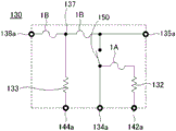
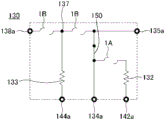
Fig. 10 (a) is a circuit diagram before the fusible conductor of the fuse element to which the present invention is applied is blown, and fig. 10 (B) is a circuit diagram after the fusible conductor of the fuse element to which the present invention is applied is blown.
Fig. 11 is a sectional view showing a modification of the fuse element to which the present invention is applied, fig. 11 (a) is a sectional view for explaining a case where a solder piece is mounted on a soluble conductor, and fig. 11 (B) is a sectional view for explaining a case where a solder piece is mounted on each of the soluble conductor and the soluble conductor.
Fig. 12 is a cross-sectional view showing another modification of the fuse element to which the present invention is applied, fig. 12 (a) is a cross-sectional view illustrating a case where a flux containing an insulator sheet is applied to a soluble conductor, and fig. 12 (B) is a cross-sectional view illustrating a case where a flux containing an insulator sheet is applied to each of the upper and lower soluble conductors.
Fig. 13 is a sectional view of a protective element to which the present invention is applied, fig. 13 (a) is a sectional view illustrating a case where a solder chip is mounted on a soluble conductor, and fig. 13 (B) is a sectional view illustrating a case where a solder chip is mounted on a soluble conductor and a solder chip is mounted under a soluble conductor, respectively.
Fig. 14 is a plan view showing a protection element to which the present invention is applied by removing a cover member, and fig. 14 (B) is a circuit diagram before a fusible conductor of the protection element to which the present invention is applied is fused.
Fig. 15 is a sectional view showing a state where a fusible conductor of a protection element to which the present invention is applied is melted.
Fig. 16 is a plan view showing the cap member removed in a state where the fusible conductor of the protection element to which the present invention is applied is blown, and fig. 16 (B) is a circuit diagram after the fusible conductor of the protection element to which the present invention is applied is blown.
Fig. 17 is a sectional view showing a modified example of the protective element to which the present invention is applied, fig. 17 (a) is a sectional view for explaining a case where a flux chip is mounted on a soluble conductor, and fig. 17 (B) is a sectional view for explaining a case where a flux chip is mounted on each of the soluble conductor and the soluble conductor.
Fig. 18 is a sectional view showing another modification of the protective element to which the present invention is applied, fig. 18 (a) is a sectional view illustrating a case where a flux containing an insulator sheet is applied to a soluble conductor, and fig. 18 (B) is a sectional view illustrating a case where a flux containing an insulator sheet is applied to each of the upper and lower soluble conductors.
Fig. 19 is a plan view showing a short-circuit element to which the present invention is applied, with a cover member removed.
Fig. 20 is a sectional view of a short-circuit element to which the present invention is applied, fig. 20 (a) is a sectional view illustrating a case where a solder chip is mounted on a soluble conductor, and fig. 20 (B) is a sectional view illustrating a case where a solder chip is mounted on a soluble conductor and a solder chip is mounted under a soluble conductor, respectively.
Fig. 21 is a sectional view showing a state where a fusible conductor of a short-circuit element to which the present invention is applied is melted.
Fig. 22 (a) is a circuit diagram before the fusible conductor of the short-circuit element to which the present invention is applied is blown, and fig. 22 (B) is a circuit diagram after the fusible conductor of the short-circuit element to which the present invention is applied is blown.
Fig. 23 is a sectional view showing a modified example of the short-circuit element to which the present invention is applied, fig. 23 (a) is a sectional view for explaining a case where a flux chip is mounted on a soluble conductor, and fig. 23 (B) is a sectional view for explaining a case where a flux chip is mounted on each of the soluble conductor and the soluble conductor.
Fig. 24 is a cross-sectional view showing another modification of the short-circuit device to which the present invention is applied, fig. 24 (a) is a cross-sectional view illustrating a case where a flux containing an insulator sheet is applied to a soluble conductor, and fig. 24 (B) is a cross-sectional view illustrating a case where a flux containing an insulator sheet is applied to each of the upper and lower soluble conductors.
Fig. 25 is a plan view showing another modification of the short-circuit element to which the present invention is applied.
Fig. 26 is a cross-sectional view showing another modification of the short-circuit element to which the present invention is applied, fig. 26 (a) is a cross-sectional view for explaining a case where a solder piece is mounted on a soluble conductor, and fig. 26 (B) is a cross-sectional view for explaining a case where a solder piece is mounted on each of the soluble conductor and the soluble conductor.
Fig. 27 is a cross-sectional view showing another modification of the short-circuit element to which the present invention is applied, fig. 27 (a) is a cross-sectional view for explaining a case where a solder piece is mounted on each of two fusible conductors, and fig. 27 (B) is a cross-sectional view for explaining a case where a solder piece is mounted on each of two fusible conductors and under each of two fusible conductors.
Fig. 28 is a cross-sectional view showing another modification of the short-circuit device to which the present invention is applied, fig. 28 (a) is a cross-sectional view for explaining a case where a solder piece is mounted on a soluble conductor, and fig. 28 (B) is a cross-sectional view for explaining a case where a solder piece is mounted on each of the soluble conductor and the soluble conductor.
Fig. 29 is a cross-sectional view showing another modification of the short-circuit element to which the present invention is applied, fig. 29 (a) is a cross-sectional view for explaining a case where a solder piece is mounted on each of two fusible conductors, and fig. 29 (B) is a cross-sectional view for explaining a case where a solder piece is mounted on each of two fusible conductors and under each of two fusible conductors.
Fig. 30 is a cross-sectional view showing another modification of the short-circuit device to which the present invention is applied, fig. 30 (a) is a cross-sectional view illustrating a case where a flux containing an insulator sheet is applied to a soluble conductor, and fig. 30 (B) is a cross-sectional view illustrating a case where a flux containing an insulator sheet is applied to each of the upper and lower soluble conductors.
Fig. 31 is a plan view showing a switching element to which the present invention is applied with a cover member removed.
Fig. 32 is a sectional view of a switching element to which the present invention is applied, fig. 32 (a) is a sectional view illustrating a case where a solder chip is mounted on a fusible conductor, and fig. 32 (B) is a sectional view illustrating a case where a solder chip is mounted on a fusible conductor and a solder chip is mounted under a fusible conductor, respectively.
Fig. 33 is a circuit diagram before a fusible conductor of a switching element to which the present invention is applied is blown.
Fig. 34 is a circuit diagram after a fusible conductor of a switching element to which the present invention is applied is blown.
Fig. 35 is a sectional view showing a state in which a fusible conductor of a switching element to which the present invention is applied is melted.
Fig. 36 is a plan view of the switching element to which the present invention is applied, with the cover member removed, showing a state in which the 2 nd fusible conductor is melted faster than the 1 st fusible conductor.
Fig. 37 is a plan view of a switching element to which the present invention is applied, with a cover member removed, and illustrates a state in which both the 1 st fusible conductor and the 2 nd fusible conductor are melted.
Fig. 38 is a sectional view showing a modified example of the switching element to which the present invention is applied, fig. 38 (a) is a sectional view for explaining a case where a solder piece is mounted on a fusible conductor, and fig. 38 (B) is a sectional view for explaining a case where a solder piece is mounted on each of the fusible conductor and the fusible conductor.
Fig. 39 is a sectional view showing another modification of the switching element to which the present invention is applied, fig. 39 (a) is a sectional view illustrating a case where a flux containing an insulator sheet is collectively applied to two fusible conductors, and fig. 39 (B) is a sectional view illustrating a case where a flux containing an insulator sheet is collectively applied to two fusible conductors and below two fusible conductors, respectively.
Fig. 40 is a sectional view showing another modification of the switching element to which the present invention is applied, fig. 40 (a) is a sectional view for explaining a case where a solder piece is individually mounted on each of two fusible conductors, and fig. 40 (B) is a sectional view for explaining a case where a solder piece is individually mounted on each of two fusible conductors and under each of two fusible conductors.
Fig. 41 is a sectional view showing another modification of the switching element to which the present invention is applied, fig. 41 (a) is a sectional view for explaining a case where a solder piece is individually mounted on each of two fusible conductors, and fig. 41 (B) is a sectional view for explaining a case where a solder piece is individually mounted on each of two fusible conductors and under each of two fusible conductors.
Fig. 42 is a cross-sectional view showing another modification of the switching element to which the present invention is applied, fig. 42 (a) is a cross-sectional view illustrating a case where a flux containing an insulator sheet is applied to each of two soluble conductors, and fig. 42 (B) is a cross-sectional view illustrating a case where a flux containing an insulator sheet is applied to each of two soluble conductors and below two soluble conductors.
Detailed Description
Hereinafter, a fuse unit, a fuse element, a protective element, a short-circuit element, and a switching element to which the present invention is applied, and a solder piece and solder used for these will be described in detail with reference to the drawings. The present invention is not limited to the following embodiments, and it is apparent that various modifications can be made without departing from the scope of the present invention. The drawings are schematic, and the proportions of the dimensions and the like may be different from those in reality. Specific dimensions and the like should be determined with reference to the following description. It is to be noted that even the drawings include portions having different dimensional relationships or ratios from each other.
[ fuse Unit ]
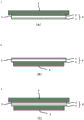
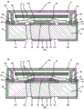
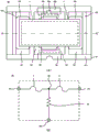
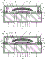
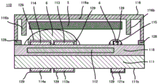
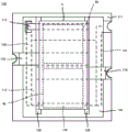
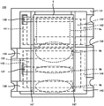
First, a fuse unit to which the present invention is applied will be described. The fuse unit 1 to which the present invention is applied is also used for a fuse element, a protection element, a short-circuit element, and a switching element described later, and is fused by self-heating (joule heat) or fused by heating of a heating element when a current exceeding a rated value is applied. The fuse unit 1 is a high melting point solder containing lead as a main component or a member in which 3 or more metal layers having different melting points are laminated. For example, in the case of a metal laminate having 3 or more layers having different melting points, as shown in fig. 1 (a), 1 (B), and 1 (C), the solder sheet 5 has a high-melting-point metal layer 2, a low-melting-point metal layer 3 having a lower melting point than the high-melting-point metal layer 2, and is formed in a substantially rectangular plate shape as shown in fig. 2, for example. The high melting point metal layer 2 and the low melting point metal layer 3 constitute a fusible conductor 6.
[ fusible conductor ]
For example, Ag, Cu, or an alloy containing Ag or Cu as a main component is suitably used for the high-melting-point metal layer 2, and has a high melting point that does not melt even when the fuse unit 1 is mounted on an insulating substrate in a reflow furnace.
For example, Sn or an alloy containing Sn as a main component, which is generally called "lead-free solder", is suitably used for the low melting point metal layer 3. The melting point of the low-melting-point metal layer 3 does not necessarily need to be higher than the temperature of the reflow furnace, and may be about 200 ℃.
The fuse unit 1 is formed by laminating 3 or more metal layers having different melting points, and thus has excellent mountability to an insulating substrate of a fuse element, a protection element, a short-circuit element, and a switching element, and also can improve mountability to an external circuit substrate of each element using the fuse unit 1. In addition, the fuse unit 1 can achieve an improvement in rating and quick fusing property in each element.
That is, even when the fuse unit 1 is exposed to a high-temperature environment of the melting point or higher of the low-melting-point metal layer 3 for a short time by an external heat source such as a reflow furnace, the fuse unit 1 is provided with the high-melting-point metal layer 2, and can prevent the fuse unit from being fused or deformed, and prevent the initial disconnection, the initial short circuit, or the degradation of fusing characteristics due to the rated fluctuation. Therefore, the fuse unit 1 can efficiently mount each element such as a fuse element on an insulating substrate or each element such as a fuse element on an external circuit substrate by reflow mounting, and can improve mountability.
Further, since the fuse unit 1 is configured by laminating the high melting point metal layer 2 having a low resistance, the conductor resistance can be significantly reduced as compared with a conventional fusible conductor using a lead-based high melting point solder. Further, by laminating the low melting point metal layer 3 and the high melting point metal layer 2, the melting temperature of the fuse unit 1 can be reduced to about 300 to 400 ℃, and the current rating can be remarkably improved as compared with a conventional chip fuse or the like having the same size and comprising a dumbbell-shaped copper foil unit having a melting point of 1085 ℃. Further, the fuse can be made thinner than a conventional chip fuse having the same current rating, and is excellent in quick fusing property.
[ flux sheet ]
In order to prevent oxidation of the high melting point metal layer 2 or the low melting point metal layer 3 of the soluble conductor 6, remove an oxide at the time of fusing, and improve solder fluidity, the fuse unit 1 is mounted with a flux sheet 5 over the entire outermost layer of the soluble conductor 6, as shown in fig. 2.
The solder piece 5 may be mounted under the fusible conductor 6 as shown in fig. 1 (B), that is, may be configured to contact the lower surface of the fusible conductor 6, in addition to being mounted on the fusible conductor 6 as shown in fig. 1 (a). When the solder piece 5 is mounted on the soluble conductor 6, it is necessary to secure a connection margin on the lower surface of the soluble conductor 6 when the fuse unit 1 is connected to the substrate of each element with the fuse unit facing downward. Therefore, the solder sheet 5 is preferably smaller in area than the lower surface of the soluble conductor 6, and may be a sheet-like body having an opening at the connection portion.
In addition to the solder pieces described with reference to fig. 1 (a) and 1 (B), the solder pieces 5 may be mounted on the fusible conductors 6 and under the fusible conductors 6, respectively, as shown in fig. 1 (C). By mounting the flux chip 5 on each of the upper and lower surfaces of the soluble conductor 6, it is expected that the oxide at the time of fusing can be removed more stably and the solder fluidity can be improved. Note that the upper and lower portions of the fusible conductor 6 of the solder chip 5 shown in fig. 1 (C) are the same as those described with reference to fig. 1 (a) and 1 (B), and therefore, the description thereof is omitted.
As shown in fig. 3 (a), 3 (B), and 3 (C), the flux sheet 5 is obtained by immersing and holding the flux 7 in a fluid or semi-fluid state in the sheet-like support 8, for example, by immersing the flux 7 in a nonwoven fabric or a mesh-like state, or by disposing a nonwoven fabric or a mesh-like state on the flux 7 applied to the outermost layer of the fuse unit 1, and immersing the flux 7. The flux sheet 5 can hold the flux 7 of a fluid or semi-fluid by a support 8 having liquid retainability.
Here, since the flux chip 5 is mounted on the fusible conductor 6 and/or under the fusible conductor 6 and used, the supporting body 8 uses an insulator so that the electrical characteristics are not affected by the fusion of the fusible conductor 6 or the like. As a material forming the support 8, various materials can be used depending on the structure thereof, and for example, an insulator such as resin or glass is suitable.
As an example of a specific structure, the flux sheet 5 is a member in which the flux 7 is impregnated in the porous support 8 in fig. 3 (a). The porous structure may be a structure having many holes penetrating in the vertical direction of the sheet as shown in fig. 3 (a), or a sponge-like structure. That is, by providing the flux chip 5 as a structure having many voids such as a porous body or a sponge, the liquid retainability is improved, and the flux 7 can be retained at a desired position on the fusible conductor 6 and/or below the fusible conductor 6.
In fig. 3 (B), the flux sheet 5 is formed by impregnating the flux 7 into a support 8, which is a nonwoven fabric or a mesh-like material. The texture is a fibrous structure as shown in fig. 3 (B). That is, the flux chip 5 can hold the flux 7 at a desired position on the fusible conductor 6 and/or under the fusible conductor 6 by improving the liquid holding property with the fibrous structure.
In fig. 3 (C), the flux sheet 5 is formed by mixing and drying a needle-like or short-fiber-like support 8 and flux 7. The needle-like shape and the short-fiber shape are described in detail in the description of the flux to be described later. The flux sheet 5 has a needle-like or short-fiber structure, and can improve liquid holding properties and hold the flux 7 at a desired position on the fusible conductor 6 and/or below the fusible conductor 6.
Here, various insulators having liquid retentivity that retain the flux 7 can be used for the support body 8, but the flux 7 needs to be retained on the fusible conductor 6 at least up to the mounting temperature of the wire unit 1 or each component using it. Therefore, the support 8 needs to have heat resistance enough to maintain its shape, and can be made of a material that deforms or melts at a temperature exceeding the mounting temperature of the fuse unit 1 or the elements using the fuse unit to have fluidity. That is, at a temperature at which the fusible conductor 6 is fused, such as exceeding the mounting temperature, it is not necessary to hold the flux 7 on the fusible conductor 6, and therefore the supporting body 8 melts and flows together with the flux 7. By melting or having fluidity of the support 8, the support 8 is not left when the fusible conductor 6 is melted, and the insulating property can be improved.
More specifically, a material that deforms or melts at a temperature of 300 ℃ or higher and has fluidity is preferably used for the support body 8.
The specific gravity of the support 8 is preferably equal to or less than the specific gravity of the soluble conductor 6. This is because the support body 8 needs to be made light to converge the fusible conductors 6 when they are fused. That is, if the specific gravity of the support 8 is larger than that of the soluble conductor 6, the support 8 presses the soluble conductor, and therefore the soluble conductor is less likely to be gathered, and the fusing characteristics as the fuse unit 1 may be deteriorated.
In the volume of the fusible conductor 6, the low melting point metal layer 3 occupies most of the volume, and therefore, the specific gravity of the support 8 is preferably set to be equal to or less than the specific gravity of the low melting point metal layer 3, and more specifically, the specific gravity is preferably set to 5g/cm3The following materials.
As shown in fig. 2, the solder pellet 5 has an area larger than the surface area of the fusible conductor 6. Thus, the fusible conductor 6 is completely covered with the solder piece 5, and even when the volume expands due to melting, rapid fusing due to the removal of oxidation of the solder 7 and the improvement of wettability can be reliably achieved. As shown in fig. 1 (B) and 1 (C), when the flux chip 5 is mounted on the lower surface of the soluble conductor 6, the area is smaller than the surface area of the soluble conductor 6. Thus, the lower surface of the fusible conductor 6 is covered with the solder piece 5, and a connection margin of each element to the substrate can be secured.
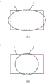
As shown in fig. 4 (a) and 4 (B), the flux chip 5 may have a circular or elliptical shape. Such a solder sheet 5 can be formed into a circular or elliptical shape by punching or the like of a sheet having a sufficiently larger surface area than the fusible conductor 6.
When the solder piece 5 is formed in a circular or elliptical shape, it is preferable that at least the diameter of the circle or ellipse is larger than the short side of the rectangular fusible conductor 6. The position for mounting the flux chip 5 is preferably a position where the center of the circle or ellipse overlaps the fusion-cut portion of the soluble conductor 6.
By mounting the flux sheet 5 on the fusible conductor 6 and/or under the fusible conductor 6, it is possible to retain the flux over the entire surface of the fusible conductor 6 even in the heat treatment step when the fuse unit 1 is mounted, to improve the wettability of the fusible conductor 6 to the low-melting-point metal layer 3 (e.g., solder), to remove the oxide during melting of the low-melting-point metal layer 3, and to improve the quick fusing property using the corrosive action to the high-melting-point metal (e.g., Ag).
Further, even when the flux chip 5 is mounted on the fusible conductor 6 and/or under the fusible conductor 6 and an oxidation preventing film such as lead-free solder containing Sn as a main component is formed on the surface of the high melting point metal layer 2 of the outermost layer of the fusible conductor 6, the oxide of the oxidation preventing film can be removed, thereby effectively preventing the oxidation of the high melting point metal layer 2 and maintaining and improving the quick fusing property.
[ flux containing insulator sheet ]
In order to obtain substantially the same effect as that of the flux sheet 5, the flux 9 containing an insulator sheet, which is contained in the needle-like or short-fiber insulator sheet 10 mixed with the flux 7 of the fluid or semi-fluid, may be applied to the fusible conductor 6 and/or under the fusible conductor 6 without immersing the fluid or semi-fluid flux 7 in the sheet-like support 8.
As shown in fig. 5 (a), the flux 9 including an insulator sheet is composed of a fluid or semi-fluid flux 7 and an insulator sheet 10 of needle-like or short fibers.
The flux 7 may be the same as the flux impregnated into the flux sheet 5.
The insulator sheet 10 is an insulator of needle-like or short fibers. For example, glass fibers or a material obtained by finely dividing a nonwoven fabric into short fibers can be used for the insulator sheet 10. The insulator sheet 10 is formed to have a length within a range not affecting the fluidity of the flux 7, and is entangled with each other when mixed with the flux 7, or has a structure having a predetermined surface area so that the flux 7 can be held between each other by surface tension.
The shape of the insulator sheet 10 is not limited to the needle shape or the short fiber, and may have a hook-like structure, for example, and may be entangled with each other by the hook-like structure. The insulator sheet 10 is not limited to a single shape, and may be different in shape or length.
The flux 9 including the insulator sheet may be applied under the soluble conductor 6, that is, applied to the lower surface of the soluble conductor 6 as shown in fig. 5 (B), in addition to being applied on the soluble conductor 6 as shown in fig. 5 (a). In addition, when the flux 9 including the insulator sheet is applied to the fusible conductor 6, and when the fuse unit 1 is connected to the substrate of each element in a downward direction, it is necessary to secure a connection margin on the lower surface of the fusible conductor 6. Therefore, the flux 9 including the insulator sheet is preferably applied so as to be smaller than the area of the lower surface of the soluble conductor 6, and is preferably applied so as to avoid the connection portion.
The flux 9 including the insulator sheet may be applied on the soluble conductor 6 and under the soluble conductor 6 as shown in fig. 5 (C), in addition to the description of fig. 5 (a) and 5 (B). By applying the flux 9 containing the insulator sheet on the upper and lower sides of the soluble conductor 6, it is expected that the oxide at the time of fusing can be removed more stably and the fluidity of the solder can be improved. Note that the flux 9 including the insulator sheet shown in fig. 5 (C) is the same as the flux described with reference to fig. 5 (a) and 5 (B) above and below the soluble conductor 6, and therefore, the description thereof is omitted.
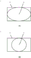
The flux 9 including the insulator sheet 10 can be applied to the soluble conductor 6 in a circular or elliptical shape as shown in fig. 6 (a) or 6 (B), thereby holding the flux 7 in the same manner as the flux sheet 5, simplifying the sheet manufacturing and sheet mounting steps as compared with the flux sheet 5, and being implemented without changing the previous manufacturing step of applying the flux to the soluble conductor.
In addition, the flux 9 containing the insulator sheet is more preferably applied in a rectangular shape over the fusible conductor 6 and/or over the entire surface below the fusible conductor 6, from the viewpoint of removing an oxide at the time of fusing and improving solder fluidity. However, it is needless to say that the flux 9 including the insulator sheet is not applied to the connection portion of each element under the soluble conductor 6, and a connection margin needs to be kept, which is the same as the case described with reference to fig. 1 (B) and 1 (C).
[ stacked Structure of fuse units ]
The fuse unit 1 can improve the resistance (pulse resistance) to surge of an abnormally high voltage instantaneously applied to an electric system in which each element such as a fuse element is incorporated, by forming the inner layer provided between the pair of high-melting-point metal layers 2 as the low-melting-point metal layer 3 and forming the outer layer as the high-melting-point metal layer 2. That is, with the fuse unit 1, the fusible conductor 6 cannot be blown, for example, in a case where a current of, for example, 100A flows for several megaseconds (msec). Here, since a large current flowing for a very short time flows on the surface layer of the conductor (skin effect), the fuse unit 1 is provided with the high-melting-point metal layer 2 such as Ag plating having a low resistance value as the outer layer of the fusible conductor 6, and therefore, the current applied by the surge is easily flowed, and the fuse unit can be prevented from being fused by the self-heating. Therefore, the fuse unit 1 can significantly improve the resistance to surge as compared with a conventional fuse made of a solder alloy.
In the fuse unit 1, the volume of the low melting point metal layer 3 of the fusible conductor 6 is preferably larger than the volume of the high melting point metal layer 2. By making the volume of the low melting point metal layer 3 large, the fuse unit 1 can efficiently perform the short-time fusing due to the erosion of the high melting point metal layer 2.
[ production method ]
The fuse unit 1 can be manufactured by forming the high melting point metal 2 on the surface of the low melting point metal layer 3 by using a plating technique to form the fusible conductor 6, and mounting the solder piece 5 on the fusible conductor 6 and/or under the fusible conductor 6.
The soluble conductor 6 can be efficiently manufactured by, for example, Ag plating on the surface of a long solder foil, and can be easily used by cutting the solder foil according to the size when used.
The fusible conductor 6 may be produced by bonding a low-melting-point metal foil constituting the low-melting-point metal layer 3 and a high-melting-point metal foil constituting the high-melting-point metal layer 2. The soluble conductor 6 can be manufactured by, for example, laminating and pressing (press) 2 pieces of rolled Cu foil or Ag foil with a similarly rolled solder foil constituting the low melting point metal layer 3 interposed therebetween. In this case, the low melting point metal foil is preferably selected to be softer than the high melting point metal foil. This makes it possible to absorb variations in thickness and to bond the low-melting-point metal foil and the high-melting-point metal foil without a gap. Since the low melting point metal foil is reduced in thickness by pressing, it is only necessary to set the thickness to be thick. When the low melting point metal foil protrudes from the end face of the soluble conductor by the pressing, the low melting point metal foil is preferably cut and finished into a shape.
The soluble conductor 6 can be formed by laminating the low melting point metal layer 3 and the high melting point metal layer 2 by a thin film forming technique using vapor deposition or the like or other known laminating technique.
In the case where one high-melting-point metal layer 2 is used as the outermost layer of the fusible conductor 6, an oxidation preventing film, not shown, may be formed on the surface of the outermost high-melting-point metal layer 2. The outermost high-melting-point metal layer 2 of the fusible conductor 6 is further covered with an oxidation-preventing film, and thus, for example, even when Cu plating or Cu foil is formed as the high-melting-point metal layer 2, oxidation of Cu can be prevented. Therefore, the soluble conductor 6 can be prevented from being fused for a long time due to oxidation of Cu, and can be fused in a short time.
The soluble conductor 6 can be formed using an inexpensive metal such as Cu, which is easily oxidized, as the high melting point metal layer 2, without using an expensive material such as Ag.
The oxidation preventing film of the high melting point metal can be made of the same material as the low melting point metal layer 3, and for example, lead-free solder containing Sn as a main component can be used. The oxidation preventing film can be formed by plating tin on the surface of the high melting point metal layer 2. The oxidation preventing film can be formed by Au plating or pre-solder.
Next, a process of mounting the flux chip 5 on the soluble conductor 6 will be described. First, the flux sheet 5 is prepared by dipping the flux 7 into the support 8 having an area sufficiently larger than that of the soluble conductor 6, heating the resultant in an oven or the like to dry and solidify the solvent portion of the flux 7, thereby preparing a mother sheet (mother sheet), and cutting the mother sheet into desired sizes. Further, the flux sheet 5 may be directly manufactured without manufacturing a master. In this case, the step of cutting out the flux sheet 5 can be omitted.
Next, the cut-out solder piece 5 is mounted on the soluble conductor 6 so as to completely cover and hide the soluble conductor 6. Further, as a fixing agent for temporarily fixing the flux chip 5 to the soluble conductor 6, a small amount of liquid flux 7 is dropped or applied, and the flux chip 5 is mounted on the soluble conductor 6 by being dried while being carried on the flux chip 5. When the solder piece 5 is mounted under the soluble conductor 6, the solder piece 5 having a smaller surface area than the lower surface of the soluble conductor 6 is mounted in a state where the lower surface of the soluble conductor 6 faces upward. Further, as a fixing agent for temporarily fixing the flux chip 5 under the soluble conductor 6, a small amount of liquid flux 7 is dropped or applied, and the flux chip 5 is mounted on the soluble conductor 6 by being dried while being carried on the flux chip 5. Further, in the case where the flux pieces 5 are mounted on the upper and lower fusible conductors 6 and 6, the flux pieces 5 may be mounted on one surface of each fusible conductor 6, but one or both of the two flux pieces 5 may be temporarily fixed, and the fixing agent may be dried by heating when bonding the cover members of the respective elements, which will be described later.
Another example in which the flux chip 5 is mounted on the soluble conductor 6 will be described. The support 8 corresponding to the size of the solder piece 5 is cut out from the mother support which is sufficiently larger than the area of the fusible conductor 6. Next, after the flux 7 is applied or dropped onto the soluble conductor 6, the cut support 8 is carried before the flux 7 is dried. The support 8 absorbs the flux 7 and is integrated with the flux 7 because of its liquid-retaining property. Thereafter, the solvent portion of the flux 7 is dried and solidified through a drying process, thereby forming the flux sheet 5. When the solder piece 5 is mounted under the soluble conductor 6, the support 8 cut out to have a smaller surface area than the lower surface of the soluble conductor 6 is carried after the flux 7 is applied or dropped onto the lower surface of the soluble conductor 6 in a state where the lower surface of the soluble conductor 6 is directed upward and before the flux is dried 7. The support 8 absorbs the flux 7 and is integrated with the flux 7 because of its liquid-retaining property. Thereafter, the solvent portion of the flux 7 is dried and solidified through the drying process, so that the flux piece 5 is formed on the lower surface of the soluble conductor 6.
By using this step, the step of manufacturing the solder sheet 5 in advance can be omitted, and the fuse unit 1 can be manufactured by simply carrying the support 8 after the ordinary step of applying the solder 7, without requiring a complicated manufacturing step.
An example of a case where the flux chip 5 is not mounted on the soluble conductor 6, that is, a case where the flux 9 including an insulator chip is used will be described. The flux 9 containing the insulator sheet on the soluble conductor 6 spreads by applying or dropping the flux 9 containing the insulator sheet having fluidity or semi-fluidity on the soluble conductor 6, and the configuration and the effect substantially equal to those of the flux sheet 5 can be obtained. In addition, when the flux 9 including the insulator sheet is applied under the soluble conductor 6, the flux 9 including the insulator sheet is applied or dropped onto the lower surface of the soluble conductor 6 in a state where the lower surface of the soluble conductor 6 faces upward, and the flux 9 including the insulator sheet spreads on the lower surface of the soluble conductor 6, whereby a structure and an effect substantially equivalent to those of the flux sheet 5 can be obtained.
By using this step, the step of manufacturing the solder sheet 5 in advance can be omitted, and the fuse unit 1 can be manufactured by applying the solder 9 containing the insulator sheet only in the same step as the ordinary step of applying the solder 7, without requiring a complicated manufacturing step.
Next, a fuse element, a protection element, a short-circuit element, and a switching element using the fuse unit 1 will be described. In the following description, each element using the fuse unit 1 will be described, but it is obvious that the fuse unit 1 and its modified examples may be used for each element. In the following, elements substantially identical to those described with reference to the fuse unit 1 are denoted by the same reference numerals, and description thereof is omitted.
[ fuse element (self-heating cutoff) ]
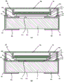
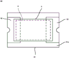
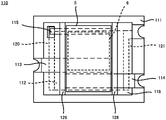
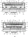
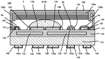
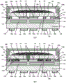
As shown in fig. 7 (a), a fuse element 80 to which the present invention is applied includes: an insulating substrate 81; a 1 st electrode 82 and a 2 nd electrode 83 provided on the insulating substrate 81; a fuse unit 1 which is installed between the 1 st and 2 nd electrodes 82, 83, and which cuts off a current path between the 1 st and 2 nd electrodes 82, 83 by applying a current exceeding a rated current and fusing by self-heating; and a cover member 89 covering the fuse unit 1 on the insulating substrate 81. The fuse unit 1 is constituted by a fusible conductor 6 and a solder piece 5 mounted on the fusible conductor 6 and/or below the fusible conductor 6.
The insulating substrate 81 is formed in a rectangular shape using an insulating member such as alumina, glass ceramic, mullite, or zirconia. In addition, a material for a printed wiring board such as an epoxy glass substrate or a phenol substrate may be used for the insulating substrate 81.
The 1 st and 2 nd electrodes 82 and 83 are formed on opposite ends of the insulating substrate 81. The 1 st and 2 nd electrodes 82 and 83 are formed by a conductive pattern such as Ag or Cu wiring, and a protective layer 86 such as Sn plating, Ni/Au plating, Ni/Pd/Au plating, or the like is provided on the surface as appropriate as a measure against oxidation. The 1 st and 2 nd electrodes 82 and 83 are continuous with the 1 st and 2 nd external connection electrodes 82a and 83a formed on the rear surface 81b from the front surface 81a of the insulating substrate 81 via a castellation (casting). The fuse element 80 is mounted on a current path of the circuit board via the 1 st and 2 nd external connection electrodes 82a and 83a formed on the rear surface 81 b.
The 1 st and 2 nd electrodes 82 and 83 are connected to the fusible conductor 6 of the fuse unit 1 via a connecting material 88 such as solder. As described above, since the fusible conductor 6 includes the high-melting-point metal layer 2, the fuse unit 1 has high mountability and can be easily connected by reflow soldering or the like after being mounted between the 1 st and 2 nd electrodes 82 and 83 via the connecting material 88.
[ fusible conductor ]
As the fusible conductor 6, a fusible conductor substantially equivalent to the fusible conductor described in the fuse unit 1 is used, and therefore, the description and the layer structure are omitted. The same applies to all the embodiments described below.
[ flux sheet ]
The fuse element 80 is mounted with a flux sheet 5 over the entire outermost layer on the soluble conductor 6, as shown in fig. 7 (a), in order to prevent oxidation of the high melting point metal layer 2 or the low melting point metal layer 3, remove oxides at the time of fusing, and improve solder fluidity. Since the solder sheet 5 is substantially the same as the solder sheet described in the fuse unit 1, the description and the internal structure are omitted. In addition, when the solder piece 5 is mounted on the fusible conductor 6, as shown in fig. 7 (B), the above-described case of the fuse unit 1 can be applied, and only an example in which the solder piece 5 is mounted on the fusible conductor 6 will be described, and detailed illustration and description will be omitted. The same applies to all the embodiments described below.
The flux sheet 5 is a sheet-shaped support 8 into which a fluid or semi-fluid flux 7 is impregnated and held, and the flux 7 is impregnated into a nonwoven fabric or a mesh, for example, or the flux 7 is impregnated by arranging a nonwoven fabric or a mesh on the flux 7 applied to the outermost layer of the soluble conductor 6.
As shown in fig. 8, the solder pellet 5 preferably has an area larger than the surface area of the fusible conductor 6. Thus, the fusible conductor 6 is completely covered with the solder piece 5, and even when the volume expands due to melting, oxidation removal by the solder 7 and rapid fusing due to improvement of wettability can be reliably achieved.
By mounting the solder piece 5 on the fusible conductor 6, the solder 7 can be held over the entire surface of the fusible conductor 6 even in the heat treatment step at the time of mounting the fuse unit 1 or at the time of mounting the fuse element 80, and when the fuse element 80 is actually used, the wettability of the low melting point metal layer 3 (e.g., solder) is improved, and the oxide during melting of the 1 st and 2 nd low melting point metals is removed, and the corrosive action on the high melting point metal (e.g., Ag) is used, whereby the quick fusing property can be improved.
Further, even when an oxidation preventing film such as a lead-free solder mainly containing Sn is formed on the surface of the high melting point metal layer 2 of the outermost layer of the soluble conductor 6 by disposing the flux chip 5, the oxide of the oxidation preventing film can be removed, so that the oxidation of the high melting point metal layer 2 can be effectively prevented, and the quick fusing property can be maintained and improved.
[ cover Member ]
The fuse element 80 is provided with a lid member 89 which protects the inside and prevents the melted fuse unit 1 from scattering, on a surface 81a of an insulating substrate 81 on which the fuse unit 1 is provided.
The lid member 89 can be formed of an insulating member such as various engineering plastics or ceramics. Since the fuse element 80 is covered with the cover member 89, even when self-heating cutoff is performed due to generation of arc discharge caused by overcurrent, the molten metal is captured by the cover member 89, and scattering to the surroundings can be prevented.
The cover member 89 has a protruding portion 89b extending from the top surface 89a toward the insulating substrate 81 to at least the side surface of the solder piece 5. Since the lid member 89 restricts the movement of the side surface of the flux chip 5 by the projection 89b, the position shift of the flux chip 5 can be prevented. That is, the projection 89b is provided at a position corresponding to the position at which the solder piece 5 is to be held, so as to have a size that maintains a predetermined gap with respect to the size of the solder piece 5. The protruding portion 89b may be a wall surface covering around the side surface of the flux pad 5, or may be a member partially protruding.
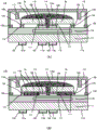
The lid member 89 is configured to have a predetermined space between the solder sheet 5 and the top surface 89 a. This is because, as shown in fig. 9, when the fusible conductor 6 is melted, the melted conductor is required to push up the gap for the solder piece 5.
Therefore, the lid member 89 is configured to: the height of the internal space of the cover member 89 (the height up to the top surface 89 a) is made larger than the sum of the height of the fused fusible conductor 6 on the surface 81a of the insulating substrate 81 (the height that becomes the highest among the fused conductors in the case of breaking into a plurality of fused conductors) and the thickness of the solder piece 5.
[ mounting state ]
Next, the mounting state of the fuse element 80 will be described. As shown in fig. 7, the fusible element 80 is mounted with the fusible conductor 6 separated from the surface 81a of the insulating substrate 81.
On the other hand, in a fuse element in which a fusible conductor or the like is formed on the surface of an insulating substrate by printing and the fusible conductor is in contact with the surface of the insulating substrate, a fusible metal of the fusible conductor adheres to the insulating substrate between electrodes 1 and 2, and leakage occurs. For example, in a fuse element in which a fusible conductor is formed by printing Ag paste on a ceramic substrate, the ceramic and Ag are sintered and cut into the fuse element, and the sintered fuse element remains between the 1 st and 2 nd electrodes. Therefore, a leakage current flows between the 1 st and 2 nd electrodes due to the residue, and the current path cannot be completely blocked.
Here, in the fuse element 80, the fusible conductor 6 is formed as a single body separately from the insulating substrate 81, and is mounted separately from the surface 81a of the insulating substrate 81. Therefore, the fuse element 80 is drawn to the 1 st and 2 nd electrodes 82 and 83 without causing the fusible metal to cut into the insulating substrate 81 even when the fusible conductor 6 is fused, and the 1 st and 2 nd electrodes 82 and 83 can be reliably insulated from each other.
The fuse element 80 can be connected to the 1 st and 2 nd electrodes 82 and 83 with the fusible conductor 6 by reflow soldering as described above, but in addition to this, the fuse element 80 may be connected to the 1 st and 2 nd electrodes 82 and 83 with the fusible conductor 6 by ultrasonic soldering.
Next, as shown in fig. 8, the fuse element 80 is mounted on the fusible conductor 6 so that the solder sheet 5 completely covers the hidden fusible conductor 6. Further, as a fixing agent for temporarily fixing the flux 5 to the soluble conductor 6, a small amount of liquid flux 7 is dropped or applied to carry the flux piece 5, thereby fixing the flux piece 5 to the soluble conductor 6.
Next, the lid member 89 is bonded to the insulating substrate 81 via the adhesive 84. The protruding portion 89b of the cover member 89 has a predetermined gap with respect to the mounting position of the flux chip 5, and therefore does not interfere with the flux chip 5.
[ Circuit diagram ]
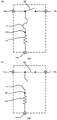
Such a fuse element 80 has a circuit configuration shown in fig. 10 (a). The fuse element 80 is mounted on an external circuit via the 1 st and 2 nd external connection electrodes 82a and 83a, and is incorporated in a current path of the external circuit. The fuse element 80 does not blow even by self-heating while a predetermined rated current flows through the fusible conductor 6. When the fuse element 80 is energized with an overcurrent exceeding the rated current, the fusible conductor 6 is fused by self-heating, and cuts off the interval between the 1 st and 2 nd electrodes 82 and 83, thereby cutting off the current path of the external circuit (fig. 10B).
At this time, since the fusible conductor 6 is laminated with the low-melting-point metal layer 3 having a lower melting point than the high-melting-point metal layer 2 as described above, the fuse element 80 starts to erode the high-melting-point metal layer 2 by self-heating due to overcurrent. Therefore, the fuse element 80 can be melted at a temperature lower than the melting temperature of the high-melting-point metal layer 2 by the action of the low-melting-point metal layer 3 of the fusible conductor 6 on the high-melting-point metal layer 2, and can be melted quickly.
Further, as shown in fig. 9, the molten metal of the soluble conductor 6 is left-right opened by the physical drawing action of the 1 st and 2 nd electrodes 82 and 83, and thus the current path between the 1 st and 2 nd electrodes 82 and 83 can be quickly and reliably cut off.
[ production method ]
The manufacturing method of the fuse element 80 can be the manufacturing method of the fuse unit 1 described above. Thus, the explanation of the manufacturing method related to the fuse unit 1 is omitted.
First, Ag or Cu wiring or the like is patterned by screen printing or the like on the 1 st and 2 nd electrodes 82 and 83, respectively, at opposite ends of the insulating substrate 81, and a protective layer 86 of Sn, Ni/Au, Ni/Pd/Au or the like is formed on the surface by electroplating as appropriate as a countermeasure against oxidation and electrode corrosion, thereby manufacturing a base portion.
Next, on the front surface 81a side of the insulating substrate 81, a connecting material 88 such as solder paste is applied to the 1 st and 2 nd electrodes 82 and 83, and the fusible conductor 6 portion of the fuse unit 1 is connected to the 1 st and 2 nd electrodes 82 and 83. Thus, the fusible conductor 6, which is the fuse unit 1, is mounted on the 1 st and 2 nd electrodes 82 and 83.
Next, the adhesive 84 is applied to the surface 81a side of the insulating substrate 81 in a predetermined range, and then the lid member 89 is adhered to cover the fuse unit 1, thereby completing the fuse element 80.
Here, as for the method of mounting the fuse unit 1 in the fuse element 80, the manufacturing process of the fuse unit 1 may be divided and employed inside the manufacturing process of the fuse element 80.
Specifically, before the solder piece 5 of the fuse unit 1 is bonded to the soluble conductor 6, or before the solder 9 containing an insulator sheet is applied to the surface of the soluble conductor 6, after the individual soluble conductor 6 is mounted on the 1 st and 2 nd electrodes 82 and 83 and connected, the solder piece 5 may be temporarily fixed to the soluble conductor 6 with a fixing agent such as a solder 7, or after the individual soluble conductor 6 is mounted on the 1 st and 2 nd electrodes 82 and 83 and connected, the solder 9 containing an insulator sheet may be applied. In this case, the flux sheet 5 can be fixed while the adhesive 84 is cured by heating in the step of bonding the cover member 89.
By adopting the method for manufacturing the fuse unit 1 in the method for manufacturing the fuse element 80, it is possible to integrate the manufacturing process of the fuse element 80 and the manufacturing process of the fuse unit 1 without manufacturing the fuse unit 1 in advance, and therefore, improvement in productivity can be expected.
Note that, even when the method for manufacturing the fuse unit 1 is adopted as the method for manufacturing the fuse element 80, the step of bonding the lid member 89 is finally unnecessary.
[ modification 1 of fuse element ]
Next, modification 1 of the fuse element 80 will be described. As shown in fig. 11 (a), the fuse element 80 may be one in which the solder piece 5 is replaced with a solder piece 85 a. The fuse element 80 shown in fig. 11 (a) is not particularly modified in portions other than the solder bumps 85 a.
The flux sheet 85a is formed by immersing and holding the flux 7 in a fluid or semi-fluid state in the sheet-like support 8, for example, by immersing the flux 7 in a nonwoven fabric or a mesh-like state, or by disposing a nonwoven fabric or a mesh-like state on the flux 7 applied to the outermost layer of the soluble conductor 6 and immersing the flux 7. The flux sheet 85a can hold the flux 7 of the fluid or semi-fluid by the support 8 having liquid retainability.
When the structure shown in modification 1 of the fuse element 80 is used, the fuse element 80 can be manufactured by mounting and connecting the single soluble conductor 6 to the 1 st and 2 nd electrodes 82 and 83, applying or dropping the flux 7 of the fluid or semi-fluid to the soluble conductor 6, and then mounting the sheet-like support 8 on the flux 7 in the manufacturing method of the fuse element 80 described above.
In addition, when the structure shown in modification 1 of the fuse element 80 is used, the solder piece 85a can be mounted under the soluble conductor 6 as shown in fig. 11 (B). It is needless to describe that the solder piece 85a may be mounted only under the fusible conductor 6.
[ modification 2 of fuse element ]
Next, a modification of the fuse element 80 will be described. As shown in fig. 12 (a), the fuse element 80 may be one in which the solder sheet 5 is replaced with solder 85b containing an insulator sheet. The fuse element 80 shown in fig. 12 (a) is not particularly modified in portions other than the solder 85b containing the insulator sheet.
The flux 85b containing the insulator sheet is contained in the insulator sheet 10 of needle-like or short fiber mixed with the flux 7 of the fluid or semi-fluid and applied to the soluble conductor 6 without immersing the fluid or semi-fluid flux 7 in the sheet-like support 8. The flux 85b including the insulator sheet can hold the fluid or semi-fluid flux 7 on the soluble conductor 6 by the insulator sheet 10 having liquid retainability.
When the structure shown in modification 2 of the fuse element 80 is used, the fuse element 80 can be manufactured by mounting and connecting the individual fusible conductors 6 to the 1 st and 2 nd electrodes 82 and 83, and then applying the flux 9 containing the insulator sheet, which is contained by mixing the needle-shaped or short-fiber insulator sheet 10, to the fusible conductors 6 in the above-described method for manufacturing the fuse element 80.
In addition, when the structure shown in modification 2 of the fuse element 80 is used, as shown in fig. 12 (B), the flux 85B containing the insulator sheet can be applied under the soluble conductor 6. It is needless to say that the flux 85b including the insulator sheet may be applied only under the fusible conductor 6.
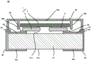
[ protective element (heating block and self-heating block by heating element) ]
Next, a protection element using the fuse unit 1 will be described. In the following description, the same components as those of the fuse unit 1 and the fuse element 80 are denoted by the same reference numerals, and the details thereof are omitted.
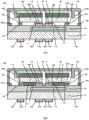
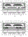
As shown in fig. 13 (a) and 14 (a), a protection element 90 to which the present invention is applied includes: an insulating substrate 91; a heating element 93 laminated on the insulating substrate 91 and covered with the insulating member 92; a 1 st electrode 94 and a 2 nd electrode 95 formed at both ends of the insulating substrate 91; a heating element extraction electrode 96 laminated on the insulating substrate 91 so as to overlap the heating element 93 and electrically connected to the heating element 93; a fuse unit 1 having both ends connected to the 1 st and 2 nd electrodes 94 and 95, respectively, and a central portion connected to a heating element extraction electrode 96; and a cover member 97 covering the fuse unit 1 on the insulating substrate 91. The fuse unit 1 is composed of a fusible conductor 6 and a solder piece 5 mounted on the fusible conductor 6 and/or under the fusible conductor 6. Fig. 13 (B) illustrates the solder piece 5 mounted under the soluble conductor 6.
The insulating substrate 91 is formed in a rectangular shape using an insulating member such as alumina, glass ceramic, mullite, or zirconia, as in the insulating substrate 81. In addition, a material for a printed wiring board such as an epoxy glass substrate or a phenol substrate may be used for the insulating substrate 91.
The 1 st and 2 nd electrodes 94 and 95 are formed at opposite ends of the insulating substrate 91. The 1 st and 2 nd electrodes 94 and 95 are formed by conductive patterns such as Ag or Cu wirings. The 1 st and 2 nd electrodes 94 and 95 are continuous with the 1 st and 2 nd external connection electrodes 94a and 95a formed on the rear surface 91b from the front surface 91a of the insulating substrate 91 via the castellation structure. The protection element 90 is incorporated in a part of a current path formed on the circuit board by connecting the 1 st and 2 nd external connection electrodes 94b and 95b formed on the rear surface 91b to connection electrodes provided on the circuit board on which the protection element 90 is mounted.
The heating element 93 is a conductive member that generates heat when energized, and is made of, for example, nichrome, W, Mo, Ru, or a material containing these. The heating element 93 can be formed by mixing a powder of these alloys, compositions, or compounds with a resin binder or the like to form a paste-like mixture, patterning the paste on the insulating substrate 91 by a screen printing technique, and then firing the paste.
In the protection element 90, the heating element 93 is covered with the insulating member 92, and the heating element extraction electrode 96 is formed so as to face the heating element 93 through the insulating member 92. The fusible conductor 6 of the fuse unit 1 is connected to the heating element-drawing electrode 96, and thus the heating element 93 is overlapped with the fusible conductor 6 via the insulating member 92 and the heating element-drawing electrode 96. The insulating member 92 is provided to protect and insulate the heating element 93 and to transmit the heat efficiency of the heating element 93 to the soluble conductor 6, and is made of, for example, a glass layer.
The heating element 93 may be formed inside the insulating member 92 laminated on the insulating substrate 91. The heating element 93 may be formed on the back surface 91b opposite to the surface of the insulating substrate 91 on which the 1 st and 2 nd electrodes 94 and 95 are formed, or may be formed adjacent to the 1 st and 2 nd electrodes 94 and 95 on the surface 91a of the insulating substrate 91. The heating element 93 may be formed inside the insulating substrate 91.
The heating element 93 has one end connected to the heating element extraction electrode 96 and the other end connected to the heating element electrode 99. The heating element-drawing electrode 96 has: a lower portion 96a formed on the surface 91a of the insulating substrate 91 and connected to the heating element 93; and an upper portion 96b laminated on the insulating member 92 so as to face the heating element 93 and connected to the fusible conductor 6 of the fuse unit 1. Thus, the heating element 93 is electrically connected to the soluble conductor 6 of the fuse unit 1 via the heating element extraction electrode 96. Further, the heating element extraction electrode 96 is disposed to face the heating element 93 via the insulating member 92, and thus the soluble conductor 6 can be melted and easily aggregated.
The heating element electrode 99 is formed on the front surface 91a of the insulating substrate 91 and is continuous with the heating element feeding electrode 99a formed on the rear surface 91b of the insulating substrate 91 via a castellated structure.
The protection element 90 extends from the 1 st electrode 94 to the 2 nd electrode 95 via the heating element lead-out electrode 96, and is connected to the fusible conductor 6 of the fuse unit 1. The fusible conductor 6 is mounted on the 1 st and 2 nd electrodes 94 and 95 and the heating element-drawing electrode 96 via a connecting material 100 such as solder, and can be easily connected by reflow soldering or the like.
As described above, since the fusible conductor 6 includes the high-melting-point metal layer 2, the fuse unit 1 has high mountability and can be easily connected by reflow soldering or the like after being mounted on the 1 st and 2 nd electrodes 94 and 95 and the heating element-drawing electrode 96 via the connecting material 100.
The 1 st and 2 nd electrodes 94 and 95, the heating element-drawing electrode 96 and the heating element electrode 99 are formed by, for example, a conductive pattern of Ag, Cu or the like, and a protective layer 98 such as Sn plating, Ni/Au plating, Ni/Pd plating or Ni/Pd/Au plating is formed on the surface as appropriate. This prevents oxidation of the surface and suppresses corrosion of the 1 st and 2 nd electrodes 94 and 95 and the heating element lead-out electrode 96 by the connecting material 100 such as the low melting point metal layer 3 of the fusible conductor 6 or the connecting solder of the fusible conductor 6.
Further, the 1 st and 2 nd electrodes 94 and 95 are formed with an outflow prevention portion 102 made of an insulating material such as glass for preventing the outflow of the fused conductor of the fusible conductor 6 or the connecting material 100 of the fuse unit 1.
The protection element 90 is connected to the heating element extraction electrode 96 via the soluble conductor 6, and constitutes a part of a current path to the heating element 93. Therefore, in the protection element 90, when the soluble conductor 6 is melted and disconnected from the external circuit, the current path to the heating element 93 is also disconnected, and therefore, the heat generation can be stopped.
[ flux sheet ]
In the protective element 90, a flux sheet 5 is mounted on the entire outermost layer of the soluble conductor 6 as shown in fig. 14 (a) in order to prevent oxidation of the high melting point metal layer 2 or the low melting point metal layer 3, remove oxides at the time of fusing, and improve solder fluidity. The flux sheet 5 is a sheet-like support 8 in which a fluid or semi-fluid flux 7 is impregnated and held, and the flux 7 is impregnated in a nonwoven fabric or a mesh-like material, for example.
The solder pellet 5 preferably has an area larger than the surface area of the fusible conductor 6. Even when the fusible conductor 6 is completely covered with the solder piece 5 and expands in volume due to melting, the oxide removal by the solder 7 and the rapid fusing by the improvement of wettability can be reliably achieved.
By disposing the flux sheet 5, the flux 7 can be held over the entire surface of the soluble conductor 6 even in the heat treatment step when the fuse unit 1 is mounted or when the protective element 90 is mounted, and when the protective element 90 is actually used, the wettability of the low melting point metal layer 3 (e.g., solder) can be improved, and the rapid fusing property can be improved by removing the oxide during melting of the 1 st and 2 nd low melting point metals and utilizing the corrosive action on the high melting point metal (e.g., Ag).
Further, even when an oxidation preventing film such as lead-free solder mainly containing Sn is formed on the surface of the outermost high melting point metal layer 2 by disposing the flux chip 5, the oxide of the oxidation preventing film can be removed, oxidation of the high melting point metal layer 2 can be effectively prevented, and the quick fusing property can be maintained and improved.
As shown in fig. 13 (B), the flux sheet 5 may be mounted under the soluble conductor 6. Further, it is not necessary to describe the configuration in which the solder piece 5 is mounted only under the fusible conductor 6.
[ cover Member ]
The fuse element 90 is provided with a cover member 97 that protects the inside and prevents the melted fuse unit 1 from scattering, on a surface 91a of the insulating substrate 91 on which the fuse unit 1 is provided.
The lid member 97 can be formed of an insulating member such as various engineering plastics or ceramics. Since the fuse element 90 is covered with the cover member 97, even when self-heating cutoff is performed due to generation of arc discharge caused by overcurrent, the molten metal is captured by the cover member 97, and scattering to the surroundings can be prevented.
The cover member 97 has a protrusion 97b extending from the top surface 97a toward the insulating substrate 81 to at least the side surface of the flux pad 5. Since the cover member 97 restricts the movement of the side surface of the flux chip 5 by the projection 97b, the position shift of the flux chip 5 can be prevented. That is, the projection 97b is provided at a position corresponding to the position at which the flux sheet 5 is to be held, in a size that maintains a predetermined gap with respect to the size of the flux sheet 5. The protrusion 97b may be a wall surface covering around the side surface of the flux chip 5, or may be a member partially protruding.
The lid member 97 is configured to have a predetermined space between the flux sheet 5 and the top surface 97 a. This is because, as shown in fig. 15, when the fusible conductor 6 is melted, the melted conductor is required to push up the gap for the solder piece 5.
Therefore, the lid member 97 is configured to: the height of the internal space of the cover member 97 (the height up to the top surface 97 a) is made larger than the sum of the height of the fused fusible conductor 6 on the surface 91a of the insulating substrate 91 (the height that becomes the highest among the fused conductors in the case of breaking into a plurality of fused conductors) and the thickness of the solder piece 5.
[ mounting state ]
Next, the mounting state of the fuse unit 1 will be described. As shown in fig. 13 (a) and 15, the fusible conductor 6 is mounted on the fuse element 90 so as to be separated from the surface 91a of the insulating substrate 91.
On the other hand, in a fuse element in which a fusible conductor such as a fusible conductor is formed by printing on the surface of an insulating substrate and the fusible conductor is in contact with the surface of the insulating substrate, the fusible metal of the fusible conductor adheres to the insulating substrate between the 1 st and 2 nd electrodes, and leakage occurs. For example, in a fuse element in which a fusible conductor is formed by printing Ag paste on a ceramic substrate, the ceramic and Ag are sintered and cut into the fuse element, and the sintered fuse element remains between the 1 st and 2 nd electrodes. Therefore, the residual material flows a leakage current between the 1 st and 2 nd electrodes, and the current path cannot be completely blocked.
Here, in the fuse element 90, the fusible conductor 6 is formed as a single body separately from the insulating substrate 91, and is mounted separately from the surface 91a of the insulating substrate 91. Therefore, the fuse element 90 is drawn to the 1 st and 2 nd electrodes 94 and 95 and the heating element-drawing electrode 96 without causing the fusible metal to cut into the insulating substrate 91 even when the fusible conductor 6 is fused, and the 1 st and 2 nd electrodes 94 and 95 can be reliably insulated from each other.
In addition, the fusible conductor 6 can be connected to the 1 st and 2 nd electrodes 94 and 95 and the heating element-drawing electrode 96 by reflow soldering in the fuse unit 1 as described above, but the fusible conductor 6 can be connected to the 1 st and 2 nd electrodes 94 and 95 and the heating element-drawing electrode 96 by ultrasonic soldering in the fuse unit 1.
Next, the mounting state of the solder sheet 5 will be described. As shown in fig. 13 (a), the fuse element 90 is mounted on the fusible conductor 6 so that the solder sheet 5 completely covers and hides the fusible conductor 6. Further, as a fixing agent temporarily fixed to the soluble conductor 6, a small amount of liquid flux 7 is dropped or applied to carry the flux chip 5, thereby fixing the flux chip 5 to the soluble conductor 6.
Next, the lid member 97 is bonded to the insulating substrate 91 via the adhesive 103. The protruding portion 97b of the cover member 97 does not interfere with the flux sheet 5 because it has a predetermined gap with respect to the mounting position of the flux sheet 5.
[ Circuit diagram and fusing Process ]
The protection element 90 to which the present invention is applied has a circuit configuration as shown in fig. 14 (B). That is, the protection element 90 has a circuit configuration including the fusible conductor 6 connected in series between the 1 st and 2 nd external connection terminals 94a and 95a via the heating element extraction electrode 96, and the heating element 93 which generates heat by passing current through the heating element extraction electrode 96 serving as a connection point of the fusible conductor 6 to melt the fusible conductor 6. In the protective element 90, the 1 st and 2 nd electrodes 94 and 95 and the heating element electrode 99 are connected to the external circuit board through the 1 st and 2 nd external connection terminals 94a and 95a and the heating element power supply terminal 99a, respectively. In the protection element 90, the fusible conductor 6 of the fuse unit 1 is thereby connected in series to the current path of the external circuit via the 1 st and 2 nd electrodes 94 and 95, and the heating element 93 is connected to the current control element provided in the external circuit via the heating element electrode 99.
When the protection element 90 having such a circuit configuration has a current path that requires the interruption of an external circuit, the heating element 93 is energized by a current control element provided in the external circuit. As a result, the protection element 90 melts the soluble conductor 6 incorporated in the current path of the external circuit by the heat generated by the heating element 93, and as shown in fig. 16 (a) and 16 (B), the melted conductor of the soluble conductor 6 is attracted to the heating element lead-out electrode 96 and the 1 st and 2 nd electrodes 94 and 95 having high wettability, and the soluble conductor 6 is melted. Thus, the fuse unit 1 can reliably fuse the 1 st electrode 94 to the heating element-drawing electrodes 96 to 2 nd electrode 95 (fig. 16B), and can cut off the current path of the external circuit. Further, the fusible conductor 6 is fused, and the power supply to the heating element 93 is also stopped.
At this time, in the fuse unit 1, since the fusible conductor 6 is formed by laminating the low-melting-point metal layer 3 having a lower melting point than the high-melting-point metal layer 2 as described above, the high-melting-point metal layer 2 starts to be eroded by self-heating due to overcurrent. Thus, the fuse unit 1 melts the high-melting-point metal layer 2 at a temperature lower than the melting temperature by the corrosive action of the low-melting-point metal layer 3 of the fusible conductor 6 on the high-melting-point metal layer 2, and can be melted quickly.
[ production method ]
The manufacturing method of the protection element 90 can use the manufacturing method of the fuse unit 1 and the manufacturing method of the fuse element 80 described above. In the following, as a method for manufacturing the protection element 90, only a portion where the fuse unit 1 is mounted on the insulating substrate 91 will be described, and detailed description of other steps will be omitted.
First, on the surface 91a side of the insulating substrate 91, the 1 st and 2 nd electrodes 94 and 95 and the heating element lead-out electrode 96 are coated with a connecting material 100 such as solder paste, and the fusible conductor 6 portion of the fuse unit 1 is connected to the 1 st and 2 nd electrodes 94 and 95 and the heating element lead-out electrode 96. Thus, the fusible conductor 6 of the fuse unit 1 is mounted on the 1 st and 2 nd electrodes 94 and 95 and the heating element-drawing electrode 96.
Next, the adhesive 103 is applied to a predetermined range on the surface 91a side of the insulating substrate 91, and then the lid member 97 is adhered to cover the fuse unit 1, thereby completing the protection element 90.
Here, as a method of mounting the fuse unit 1 in the protection element 90, the manufacturing process of the fuse unit 1 may be divided and employed inside the manufacturing process of the protection element 90.
Specifically, before the solder piece 5 of the fuse unit 1 is bonded to the soluble conductor 6, or before the solder 9 containing the insulator piece is applied to the surface of the soluble conductor 6, after the individual soluble conductor 6 is mounted on the 1 st and 2 nd electrodes 94 and 95 and the heating element lead-out electrode 96 and connected, the solder piece 5 may be bonded to the soluble conductor 6 with a fixing agent such as solder 7 for temporary fixation, or after the individual soluble conductor 6 is mounted on the 1 st and 2 nd electrodes 82 and 83 and connected, the solder 9 containing the insulator piece may be applied.
By adopting the method for manufacturing the protection element 90 in the method for manufacturing the fuse unit 1, it is possible to integrate the manufacturing process of the fuse unit 1 and the manufacturing process of the protection element 90 without manufacturing the fuse unit 1 in advance, and thus improvement in productivity can be expected.
Even when the method for manufacturing the fuse unit 1 is used in the method for manufacturing the protection element 90, the process for bonding the cover member 97 is not described in detail.
[ modification 1 of protective element ]
Next, modification 1 of the protection element 90 will be described. As shown in fig. 17 (a), the protective element 90 may be formed by replacing the solder piece 5 with a solder piece 104 a. The protective element 90 shown in fig. 17 (a) is not particularly modified in portions other than the flux chip 104 a.
The flux sheet 104a is formed by immersing and holding the flux 7 in a fluid or semi-fluid state in the sheet-like support 8, for example, by immersing the flux 7 in a nonwoven fabric or a mesh-like state, or by disposing a nonwoven fabric or a mesh-like state on the flux 7 applied to the outermost layer of the soluble conductor 6 and immersing the flux 7. The flux sheet 104a can hold the flux 7 of the fluid or semi-fluid by the support 8 having liquid retainability.
When the structure shown in modification 1 of the protective element 90 is used, the structure can be manufactured by mounting and connecting the soluble conductor 6 alone on the 1 st and 2 nd electrodes 94 and 95 and the heating element lead-out electrode 96 in the above-described method for manufacturing the protective element 90, applying or dropping the flux 7 of the fluid or semi-fluid to the soluble conductor 6, and mounting the sheet-like support 8 on the flux 7.
In addition, when the structure shown in modification 1 of the protective element 90 is used, the flux chip 104a can be mounted under the soluble conductor 6 as shown in fig. 17 (B). Further, it is not necessary to describe the configuration in which the solder piece 104a is mounted only under the fusible conductor 6.
[ modification 2 of protective element ]
Next, modification 2 of the protection element 90 will be described. As shown in fig. 18 (a), the protective element 90 may be formed by replacing the flux sheet 5 with flux 104b containing an insulator sheet. The protective element 90 shown in fig. 18 (a) is not particularly modified in portions other than the flux 104b including the insulator sheet.
The flux 104b containing the insulator sheet is obtained by mixing the needle-shaped or short-fiber insulator sheet 10 with the fluid or semi-fluid flux 7, applying the mixture to the soluble conductor 6, and drying the mixture, without immersing the fluid or semi-fluid flux 7 in the sheet-shaped support 8. The flux 104b including the insulator sheet can hold the fluid or semi-fluid flux 7 on the soluble conductor 6 by the insulator sheet 10 having liquid retainability.
When the structure shown in modification 2 of the protective element 90 is used, the structure can be manufactured by mounting the soluble conductor 6 alone on the 1 st and 2 nd electrodes 94 and 95 and the heating element lead-out electrode 96 and then applying the flux 104b containing the insulator sheet, which is obtained by kneading the needle-like or short-fiber insulator sheet 10, to the soluble conductor 6 in the above-described method for manufacturing the protective element 90.
In addition, when the structure shown in modification 2 of the protective element 90 is used, as shown in fig. 18 (B), the flux 104B containing the insulator sheet can be applied under the soluble conductor 6. Further, it is not necessary to describe that the flux 104b including the insulator sheet is applied only under the fusible conductor 6.
[ modification 3 of protective element ]
The protective element 90 does not necessarily have to cover the heating element 93 with the insulating member 92, and the heating element 93 may be provided inside the insulating substrate 91. The material of the insulating substrate 91 is a material having excellent thermal conductivity, and the heating element 93 can be heated similarly to the case of the insulating member 92 via a glass layer or the like.
[ modification 4 of protective element ]
In the protective element 90, the heating element 93 may be provided on the rear surface 91b side of the insulating substrate 91, in addition to the heating element 93 being formed on the front surface 91a side of the insulating substrate 91 as described above. By forming the heating element 93 on the rear surface 91b of the insulating substrate 91, it is possible to form the heating element in a simpler process than in the insulating substrate 91. In this case, it is preferable to form the insulating member 92 on the heating element 93 in terms of protection of the resistor or ensuring insulation at the time of mounting.
[ short-circuit element (short-circuit by heat-generating body) ]
Next, a short-circuit element using the fuse unit 1 will be described. Fig. 19 shows a plan view of the short-circuit element 110, and fig. 20 (a) shows a cross-sectional view of the short-circuit element 110. The short-circuit element 110 includes: an insulating substrate 111; a heating element 112 provided on the insulating substrate 111; a 1 st electrode 113 and a 2 nd electrode 114 provided adjacent to each other on an insulating substrate 111; a 3 rd electrode 115 provided adjacent to the 1 st electrode 113 and electrically connected to the heating element 112; a fuse unit 1 which is provided between the 1 st and 3 rd electrodes 113 and 115 to form a current path, melts the current path between the 1 st and 3 rd electrodes 113 and 115 by heating from the heating element 112, and short-circuits the 1 st and 2 nd electrodes 113 and 114 via a melt conductor; and a cover member 116 covering the fuse unit 1 on the insulating substrate 91. The fuse unit 1 is composed of a fusible conductor 6 and a solder piece 5 mounted on the fusible conductor 6 and/or under the fusible conductor 6. Fig. 20 (B) illustrates the solder piece 5 mounted under the soluble conductor 6.
The insulating substrate 111 is formed in a substantially rectangular shape using an insulating member such as alumina, glass ceramic, mullite, or zirconia. In addition, although a material for a printed wiring board such as an epoxy glass substrate or a phenol substrate may be used for the insulating substrate 111, it is necessary to keep track of the temperature at which the fuse is blown.
The heating element 112 is covered with an insulating member 118 on the insulating substrate 111. Further, 1 st to 3 rd electrodes 113 to 115 are formed on the insulating member 118. The insulating member 118 is provided to efficiently transmit heat of the heating element 112 to the 1 st to 3 rd electrodes 113 to 115, and is formed of, for example, a glass layer. The heating element 112 can easily condense the melt conductor by heating the 1 st to 3 rd electrodes 113 to 115.
The 1 st to 3 rd electrodes 113 to 115 are formed by a conductive pattern such as Ag or Cu wiring. The 1 st electrode 113 is formed adjacent to the 2 nd electrode 114 on one side, and is insulated. A 3 rd electrode 115 is formed on the other side of the 1 st electrode 113. The 1 st electrode 113 and the 3 rd electrode 115 are electrically connected to the fusible conductor 6 of the fuse unit 1, and constitute a current path of the short-circuit element 110. The 1 st electrode 113 is connected to a 1 st external connection terminal 113a provided on the rear surface 111b of the insulating substrate 111 via a castellation structure facing the side surface of the insulating substrate 111. The 2 nd electrode 114 is connected to a 2 nd external connection terminal 114a provided on the rear surface 111b of the insulating substrate 111 via a serration structure facing the side surface of the insulating substrate 111.
The 3 rd electrode 115 is connected to the heating element 112 via a heating element extraction electrode 120 provided on the insulating substrate 111 or the insulating member 118. The heating element 112 is connected to a heating element power supply terminal 121a provided on the rear surface 111b of the insulating substrate 111 via a tooth structure facing the heating element electrode 121 and the side edge of the insulating substrate 111.
The 1 st and 3 rd electrodes 113 and 115 are connected to the fusible conductor 6 of the fuse unit 1 via a connecting material 117 such as solder. As described above, since the fusible conductor 6 includes the high-melting-point metal layer 2, the fuse unit 1 has excellent mountability and can be easily connected by reflow soldering or the like after being mounted between the 1 st and 3 rd electrodes 113 and 115 via the connecting material 117. The fuse unit 1 may be connected to the 1 st and 3 rd electrodes 113 and 115 by using the low melting point metal layer 3 provided at the lowermost layer of the soluble conductor 6 as a connecting material.
The 1 st to 3 rd electrodes 113, 114, 115 can be formed using a general electrode material such as Cu or Ag, but it is preferable to form a protective layer 129 such as Ni/Au plating, Ni/Pd/Au plating or the like on at least the surfaces of the 1 st and 2 nd electrodes 113, 114 by a known plating treatment. This prevents oxidation of the 1 st and 2 nd electrodes 113 and 114, and reliably holds the melt conductor. In addition, when the short-circuit element 110 is mounted by reflow, the solder connecting the fusible conductors 6 of the fuse unit 1 or the 1 st or 2 nd low-melting-point metal layers 3 and 4 forming the outer layers of the fusible conductors 6 of the fuse unit 1 are melted, whereby the 1 st electrode 113 can be prevented from being corroded (solder corrosion).
Further, the 1 st to 3 rd electrodes 113 to 115 are formed with anti-flowing-out portions 126 made of an insulating material such as glass for preventing the fused conductor of the fusible conductor 6 and the connecting material 117 of the fuse unit 1 from flowing out.
[ flux sheet ]
In the short-circuit element 110, a flux sheet 5 is mounted on the entire outermost layer of the soluble conductor 6 as shown in fig. 19 in order to prevent oxidation of the high-melting-point metal layer 2 or the low-melting-point metal layer 3, remove oxides at the time of fusing, and improve solder fluidity. The flux sheet 5 is a sheet-like support 8 in which a fluid or semi-fluid flux 7 is impregnated and held, and the flux 7 is impregnated in a nonwoven fabric or a mesh-like material, for example.
The solder pellet 5 preferably has an area larger than the surface area of the fusible conductor 6. Even when the fusible conductor 6 is completely covered with the solder piece 5 and expands in volume due to melting, the oxide removal by the solder 7 and the rapid fusing by the improvement of wettability can be reliably achieved.
By disposing the flux sheet 5, the flux 7 can be held over the entire surface of the soluble conductor 6 even in the heat treatment step when the fuse unit 1 is mounted or when the short-circuit element 110 is mounted, and when the short-circuit element 110 is actually used, the wettability of the low-melting-point metal layer 3 (e.g., solder) can be improved, and the rapid fusing property can be improved by removing the oxide during melting of the low-melting-point metal and using the corrosive action on the high-melting-point metal (e.g., Ag).
Further, even when an oxidation preventing film such as a lead-free solder mainly containing Sn is formed on the surface of the high melting point metal layer 2 of the outermost layer of the soluble conductor 6 by disposing the flux chip 5, the oxide of the oxidation preventing film can be removed, so that the oxidation of the high melting point metal layer 2 can be effectively prevented, and the quick fusing property can be maintained and improved.
As shown in fig. 20 (B), the flux sheet 5 may be mounted under the soluble conductor 6. Further, it is not necessary to describe the configuration in which the solder piece 5 is mounted only under the fusible conductor 6.
[ cover Member ]
The short-circuiting element 110 is provided with a cover member 116 which protects the inside and prevents the melted fuse unit 1 from scattering, on the surface 111a of the insulating substrate 111 on which the fuse unit 1 is provided.
The cover member 116 can be formed of an insulating member such as various engineering plastics or ceramics. Since the fuse unit 1 is covered with the cover member 116, the short-circuit element 110 can prevent the molten metal from being scattered to the surroundings by being captured by the cover member 116 even when the self-heating cutoff is performed due to the generation of arc discharge caused by overcurrent.
The cover member 116 has a protrusion 116b extending from the top surface 116a toward the insulating substrate 111 at least to the side surface of the flux pad 5. The cover member 116 restricts the movement of the side surface of the flux chip 5 by the projection 116b, and thus can prevent the displacement of the flux chip 5. That is, the projection 116b is provided at a position corresponding to the position at which the solder piece 5 is to be held, in a size that maintains a predetermined gap with respect to the size of the solder piece 5. The protrusion 116b may be a wall surface covering around the side surface of the flux chip 5, or may be a member partially protruding.
The lid member 116 is configured to have a predetermined gap between the flux sheet 5 and the top surface 116 a. This is because, as shown in fig. 21, when the fusible conductor 6 is melted, the melted conductor is required to push up the gap for the solder piece 5.
Therefore, the lid member 116 is configured to: the height of the internal space of the cover member 116 (the height up to the top surface 116 a) is made larger than the sum of the height of the fused fusible conductor 6 on the surface 111a of the insulating substrate 111 (the height that becomes the highest among the fused conductors in the case of breaking into a plurality of fused conductors) and the thickness of the solder piece 5.
[ short-circuit element circuit ]
The short-circuit element 110 as described above has a circuit configuration as shown in fig. 22 (a) and 22 (B). That is, in the short-circuit element 110, the 1 st electrode 113 and the 2 nd electrode 114 are insulated in a normal state (fig. 22 (a)), and when the soluble conductor 6 melts due to heat generation of the heating element 112, a switch 123 short-circuited via the molten conductor is configured (fig. 22 (B)). Further, the 1 st external connection terminal 113a and the 2 nd external connection terminal 114a constitute both terminals of the switch 123. The soluble conductor 6 is connected to the heating element 112 via the 3 rd electrode 115 and the heating element-drawing electrode 120.
When the short-circuit element 110 is incorporated in an electronic device or the like, the terminals 113a and 114a of the switch 123 are connected to a current path of the electronic device, and the current path is turned on, the switch 123 is short-circuited to form a current path of the electronic component.
For example, in the short-circuit element 110, the electronic component provided on the current path of the electronic component is connected in parallel to the terminals 113a and 114a of the switch 123, and when an abnormality occurs in the parallel-connected electronic component, electric power is supplied between the heating element power supply terminal 121a and the 1 st external connection terminal 113a, and the heating element 112 is energized to generate heat. When the soluble conductor 6 melts down by the heat, the molten conductor is condensed on the 1 st and 2 nd electrodes 113 and 114 as shown in fig. 21. Since the 1 st and 2 nd electrodes 113 and 114 are formed adjacent to each other, the fused conductors aggregated on the 1 st and 2 nd electrodes 113 and 114 are joined to each other, whereby the 1 st and 2 nd electrodes 113 and 114 are short-circuited. That is, the short-circuiting element 110 has a short circuit between both terminals of the switch 123 (fig. 22B), and forms a bypass current path for bypassing the electronic component causing the abnormality. Further, since the fusible conductor 6 is fused to fuse the 1 st and 3 rd electrodes 113 and 115, the power supply to the heating element 112 is also stopped.
[ production method ]
As the method for manufacturing the short-circuit element 110, the method for manufacturing the fuse unit 1 and the methods for manufacturing the fuse element 80 and the protection element 90 described above can be used. In the following, as a method for manufacturing the short-circuit element 110, only a portion where the fuse unit 1 is mounted on the insulating substrate 111 will be described, and detailed description of other steps will be omitted.
First, on the surface 111a side of the insulating substrate 111, a connecting material 117 such as solder paste is applied to the 1 st and 3 rd electrodes 113 and 115, and the fusible conductor 6 portion of the fuse unit 1 is connected between the 1 st and 3 rd electrodes 113 and 115. Thereby, the fusible conductor 6 of the fuse unit 1 is mounted on the 1 st and 3 rd electrodes 113 and 115.
Next, the adhesive 128 is applied to the surface 111a side of the insulating substrate 111 in a predetermined range, and then the lid member 116 is adhered with the adhesive 128 to cover the fuse unit 1, thereby completing the short-circuit element 110. The protrusion 116b of the cover member 116 has a predetermined gap with respect to the mounting position of the flux chip 5, and therefore does not interfere with the flux chip 5.
Here, as for the method of mounting the fuse unit 1 in the short-circuit element 110, the manufacturing process of the fuse unit 1 may be divided and employed inside the manufacturing process of the short-circuit element 110.
Specifically, before the solder sheet 5 of the fuse unit 1 is bonded to the soluble conductor 6, the soluble conductor 6 alone may be mounted on the 1 st and 3 rd electrodes 113 and 115 and connected, and the solder sheet 5 may be bonded to the soluble conductor 6 using a fixing agent such as solder 7 for temporary fixation. As another example, the fusible conductor 6 alone may be mounted on the 1 st and 3 rd electrodes 113 and 115 and connected, and the flux 9 including the insulator sheet may be applied on the fusible conductor 6 and dried. As another example, the individual soluble conductor 6 may be mounted on the 1 st and 3 rd electrodes 113 and 115 and connected, the flux 7 may be dropped or applied onto the soluble conductor 6, the support 8 having liquid retentivity may be placed on the flux 7 before the flux 7 is dried to absorb the flux 7, and then the flux 7 may be dried.
By adopting the method for manufacturing the short-circuit element 110 in the method for manufacturing the fuse unit 1, it is possible to integrate the manufacturing process of the fuse unit 1 and the manufacturing process of the short-circuit element 110 without manufacturing the fuse unit 1 in advance, and thus improvement in productivity can be expected.
Even when the method for manufacturing the fuse unit 1 is used in the method for manufacturing the short-circuit element 110, the process for bonding the cover member 116 is not described in detail.
[ modification 1 of short-circuiting device ]
Next, modification 1 of the short-circuit element 110 will be described. As shown in fig. 23 (a), the short-circuiting element 110 may be one in which the pad 5 is replaced with a pad 119 a. The short-circuiting element 110 shown in fig. 23 (a) is not particularly modified in portions other than the solder piece 119 a.
The flux piece 119a is formed by immersing and holding the flux 7 in a fluid or semi-fluid state in the sheet-like support 8, for example, by immersing the flux 7 in a nonwoven fabric or a mesh-like state, or by disposing a nonwoven fabric or a mesh-like state on the flux 7 applied to the outermost layer of the soluble conductor 6 and immersing the flux 7. The flux piece 119a can hold the flux 7 of the fluid or semi-fluid by the support 8 having liquid retainability.
When the structure shown in modification 1 of the short-circuit element 110 is used, the structure can be manufactured by mounting and connecting the single soluble conductor 6 to the 1 st and 3 rd electrodes 113 and 115, applying or dropping the flux 7 of the fluid or semi-fluid to the soluble conductor 6, and then mounting the sheet-like support 8 on the flux 7 in the method for manufacturing the short-circuit element 110 described above.
As shown in fig. 23 (B), a solder piece 119a may be mounted under the soluble conductor 6. Further, it is not necessary to describe any more to mount the solder piece 119a only under the fusible conductor 6.
[ modification 2 of short-circuiting device ]
Next, a modified example 2 of the short-circuit element 110 will be described. As shown in fig. 24 (a), the short-circuiting element 110 may be formed by replacing the flux chip 5 with a flux 119b containing an insulator chip. The short-circuiting element 110 shown in fig. 24 (a) is not particularly modified in the portion other than the flux 119b including the insulator sheet.
The flux 119b including an insulator sheet is applied to the soluble conductor 6 by uniformly mixing the needle-shaped or short-fiber insulator sheet 10 with the flux 7 of the fluid or semi-fluid without immersing the fluid or semi-fluid flux 7 in the sheet-shaped support 8. In the flux 119b including an insulator sheet, the fluid or semi-fluid flux 7 can be held on the soluble conductor 6 by the insulator sheet 10 having liquid retainability.
When the structure shown in modification 2 of the short-circuit element 110 is used, the short-circuit element 110 can be manufactured by mounting the soluble conductor 6 alone on the 1 st and 3 rd electrodes 113 and 115 and then applying the flux 119b containing the insulator sheet, which is obtained by kneading the needle-shaped or short-fiber insulator sheet 10, to the soluble conductor 6 in the method for manufacturing the short-circuit element 110 described above.
As shown in fig. 24 (B), a flux 119B containing an insulator sheet may be applied under the soluble conductor 6. It is needless to say that the flux 119b including the insulator sheet may be applied only under the fusible conductor 6.
[ modification 3 of short-circuiting device ]
The short-circuit element 110 does not necessarily have to cover the heating element 112 with the insulating member 118, and the heating element 112 may be provided inside the insulating substrate 111. The material of the insulating substrate 111 is a material having excellent thermal conductivity, and the heating element 112 can be heated similarly to the case of the insulating member 118 via a glass layer or the like.
[ modification 4 of short-circuiting device ]
In addition, in the short-circuiting element 110, the heating element 112 may be formed on the insulating substrate 111 on the side of the surface on which the 1 st to 3 rd electrodes 113 to 115 are formed, or the heating element 112 may be provided on the surface of the insulating substrate 111 opposite to the surface on which the 1 st to 3 rd electrodes 113 to 115 are formed. The heating element 112 can be formed in a simpler process than in the insulating substrate 111 by forming it on the rear surface 111b of the insulating substrate 111. In this case, it is preferable to form the insulating member 118 on the heating element 112 in terms of protection of the resistor or ensuring insulation at the time of mounting.
[ modification 5 of short-circuiting device ]
Further, the short-circuiting element 110 may be formed such that the heating element 112 is provided on the surface of the insulating substrate 111 on which the 1 st to 3 rd electrodes 113 to 115 are formed and is provided together with the 1 st to 3 rd electrodes 113 to 115. The heating element 112 can be formed in a simpler process than in the insulating substrate 111 by forming it on the surface of the insulating substrate 111. In this case, too, it is preferable to form the insulating member 118 on the heating element 112.
[ modification 6 of short-circuiting device ]
As shown in fig. 25 and 26 (a), the shorting element 110 may have a 4 th electrode 124 adjacent to the 2 nd electrode 114 and a 2 nd fusible conductor 6b mounted between the 2 nd and 4 th electrodes 114 and 124. The 2 nd fusible conductor 6b has the same structure as the fusible conductor 6. Note that, in modification 6 of the short-circuit element 110 and thereafter, the fusible conductor 6 is illustrated and described as the 1 st fusible conductor 6a for the purpose of distinguishing from the 2 nd fusible conductor 6 b.
[ flux sheet ]
In the short-circuit element 110, as shown in fig. 25 and 26 (a), a flux chip 5 is mounted on the entire outermost layer of the 1 st soluble conductor 6a and the 2 nd soluble conductor 6b in order to prevent oxidation of the high melting point metal layer 2 or the low melting point metal layer 3, remove oxides at the time of fusing, and improve solder fluidity. The flux sheet 5 is a sheet-like support 8 in which a fluid or semi-fluid flux 7 is impregnated and held, and the flux 7 is impregnated in a nonwoven fabric or a mesh-like material, for example.
The solder piece 5 preferably has an area larger than the total surface area of the 1 st fusible conductor 6a and the 2 nd fusible conductor 6 b. Accordingly, even when the 1 st soluble conductor 6a and the 2 nd soluble conductor 6b are completely covered with the solder piece 5 and expand in volume due to melting, the oxide removal by the solder 7 and the rapid fusing by the improvement of wettability can be reliably achieved.
By disposing the flux sheet 5, the flux 7 can be held over the entire surfaces of the 1 st soluble conductor 6a and the 2 nd soluble conductor 6b even in the heat treatment step when the fuse unit 1 is mounted or when the short-circuit element 110 is mounted, and when the short-circuit element 110 is actually used, the wettability of the low-melting-point metal layer 3 (e.g., solder) can be improved, and the rapid fusing property can be improved by removing the oxide during melting of the 1 st and 2 nd low-melting-point metals and using the corrosive action on the high-melting-point metal (e.g., Ag).
Further, even when an oxidation preventing film such as a lead-free solder mainly containing Sn is formed on the surface of the high melting point metal layer 2 of the outermost layer of the 1 st soluble conductor 6a and the 2 nd soluble conductor 6b by disposing the flux chip 5, the oxide of the oxidation preventing film can be removed, the oxidation of the high melting point metal layer 2 can be effectively prevented, and the quick fusing property can be maintained and improved.
As shown in fig. 26 (B), the solder chip 5 may be mounted under the 1 st soluble conductor 6a and the 2 nd soluble conductor 6B. It is needless to describe that the solder piece 5 may be mounted only under the 1 st soluble conductor 6a and the 2 nd soluble conductor 6 b.
[ modification 7 of short-circuiting device ]
As shown in fig. 27 (a), the short-circuiting element 110 may be mounted on each of the 1 st and 2 nd fusible conductors 6a and 6b by dividing the solder piece 5.
As shown in fig. 27 (B), the solder pieces 5 may be mounted under the 1 st soluble conductor 6a and the 2 nd soluble conductor 6B, respectively. It is needless to say that the solder pieces 5 may be individually mounted only under the 1 st soluble conductor 6a and the 2 nd soluble conductor 6 b.
[ modification 8 of short-circuiting device ]
As shown in fig. 28 (a), the short-circuiting element 110 may be configured such that after the flux 7 is applied to each of the 1 st soluble conductor 6a and the 2 nd soluble conductor 6b, the holding member 8 made of a nonwoven fabric or a mesh is mounted on the 1 st soluble conductor 6a and the 2 nd soluble conductor 6 b.
As shown in fig. 28 (B), the solder chip 5 may be mounted under the 1 st soluble conductor 6a and the 2 nd soluble conductor 6B. It is needless to describe that the solder piece 5 may be mounted only under the 1 st soluble conductor 6a and the 2 nd soluble conductor 6 b.
[ modification 9 of short-circuiting device ]
As shown in fig. 29 (a), the short-circuiting element 110 may be configured such that after the flux 7 is applied to each of the 1 st soluble conductor 6a and the 2 nd soluble conductor 6b, the holding body 8 made of a nonwoven fabric or a mesh is divided in correspondence with the 1 st soluble conductor 6a and the 2 nd soluble conductor 6b, and is individually supported on the 1 st soluble conductor 6a and the 2 nd soluble conductor 6 b.
As shown in fig. 29 (B), the solder pieces 5 may be mounted individually under the 1 st soluble conductor 6a and the 2 nd soluble conductor 6B. It is needless to say that the solder pieces 5 may be individually mounted only under the 1 st soluble conductor 6a and the 2 nd soluble conductor 6 b.
[ modification 10 of short-circuiting device ]
As shown in fig. 30 (a), the short-circuiting device 110 may be configured such that the flux 119b containing the insulator sheet of the insulator sheet 10 is uniformly mixed with the flux 7 of the convective or semi-conductive body applied to the 1 st fusible conductor 6a and the 2 nd fusible conductor 6 b.
As shown in fig. 30 (B), the flux 119B containing the insulator sheet may be applied to the 1 st soluble conductor 6a and the 2 nd soluble conductor 6B, respectively. It is needless to say that the flux 119b containing the insulator sheet may be applied individually only under the 1 st soluble conductor 6a and the 2 nd soluble conductor 6 b.
In the short-circuit element 110 shown in fig. 26 to 30, the 1 st and 2 nd electrodes 113 and 114 preferably have larger areas than the 3 rd and 4 th electrodes 115 and 124. Thus, the short-circuiting element 110 can cause more of the fused conductor to be condensed on the 1 st and 2 nd electrodes 113 and 114, and can reliably short-circuit between the 1 st and 2 nd electrodes 113 and 114.
[ switching element ]
Next, a switching element using the fuse unit 1 will be described. Fig. 31 shows a plan view of the switching element 130 and fig. 32 (a) shows a cross-sectional view of the switching element 130. The switching element 130 includes: an insulating substrate 131; a 1 st heating element 132 and a 2 nd heating element 133 provided on the insulating substrate 131; a 1 st electrode 134 and a 2 nd electrode 135 provided adjacent to each other on the insulating substrate 131; a 3 rd electrode 136 provided adjacent to the 1 st electrode 134 and electrically connected to the 1 st heating element 132; a 4 th electrode 137 provided adjacent to the 2 nd electrode 135 and electrically connected to the 2 nd heating element 133; a 5 th electrode 138 provided adjacent to the 4 th electrode 137; a 1 st soluble conductor 6a which constitutes a current path by being provided between the 1 st and 3 rd electrodes 134, 136, and fuses the current path between the 1 st and 3 rd electrodes 134, 136 by heating from the 1 st heating element 132; a 2 nd fusible conductor 6b provided from the 2 nd electrode 135 to the 5 th electrode 138 via the 4 th electrode 137, and fusing a current path between the 2 nd, 4 th, and 5 th electrodes 135, 137, and 138 by heating from the 2 nd heating element 133; a solder piece 5 mounted on the 1 st soluble conductor 6a and the 2 nd soluble conductor 6 b; and a lid member 139 for protecting the inside on the insulating substrate 131. The fuse unit 1 includes the 1 st and 2 nd fusible conductors 6a and 6b and the solder piece 5 mounted on the 1 st and 2 nd fusible conductors 6a and 6b and/or under the 1 st and 2 nd fusible conductors 6a and 6 b. Fig. 32 (B) illustrates the solder piece 5 mounted under the 1 st fusible conductor 6a and the 2 nd fusible conductor 6B.
The insulating substrate 131 is formed in a rectangular shape using an insulating member such as alumina, glass ceramic, mullite, or zirconia. The insulating substrate 131 may be made of a material for a printed wiring board such as an epoxy glass substrate or a phenol substrate.
The 1 st and 2 nd heating elements 132 and 133 are conductive members that generate heat when energized, similarly to the heating element 93 described above, and can be formed similarly to the heating element 93. The 1 st fusible conductor 6a and the 2 nd fusible conductor 6b have the same configuration as the above-described fusible conductor 6.
The 1 st and 2 nd heating elements 132 and 133 are covered with the insulating member 140 on the insulating substrate 131. The 1 st and 3 rd electrodes 134 and 136 are formed on the insulating member 140 covering the 1 st heating element 132, and the 2 nd, 4 th and 5 th electrodes 135, 137 and 138 are formed on the insulating member 140 covering the 2 nd heating element 133. The 1 st electrode 134 is formed adjacent to the 2 nd electrode 135 on one side and is insulated. A 3 rd electrode 136 is formed on the other side of the 1 st electrode 134. The 1 st electrode 134 and the 3 rd electrode 135 are electrically connected to the 1 st fusible conductor 6a, and constitute a current short-circuit path of the switching element 130. The 1 st electrode 134 is connected to the 1 st external connection terminal 134a provided on the rear surface 131b of the insulating substrate 131 via a castellation structure facing the side surface of the insulating substrate 131.
The 3 rd electrode 136 is connected to the 1 st heating element 132 via a 1 st heating element extraction electrode 141 provided on the insulating substrate 131 or the insulating member 140. The 1 st heating element 132 is connected to a 1 st heating element power supply terminal 142a provided on the rear surface 131b of the insulating substrate 131 via a tooth structure facing the 1 st heating element electrode 142 and the side edge of the insulating substrate 131.
A 4 th electrode 137 is formed on the other side of the 2 nd electrode 135 opposite to the side adjacent to the 1 st electrode 134. Further, a 5 th electrode 138 is formed on the 4 th electrode 137 on the side opposite to the side adjacent to the 2 nd electrode 135. The 2 nd electrode 135, the 4 th electrode 137, and the 5 th electrode 138 are connected to the 2 nd fusible conductor 6 b. The 2 nd electrode 135 is connected to the 2 nd external connection terminal 135a provided on the rear surface 131b of the insulating substrate 131 via a serration structure facing the side surface of the insulating substrate 131.
The 4 th electrode 137 is connected to the 2 nd heating element 133 via a 2 nd heating element extraction electrode 143 provided on the insulating substrate 131 or the insulating member 140. The 2 nd heating element 133 is connected to a 2 nd heating element power supply terminal 144a provided on the rear surface 131b of the insulating substrate 131 via a tooth structure facing the 2 nd heating element electrode 144 and the side edge of the insulating substrate 131.
Further, the 5 th electrode 138 is connected to a 5 th external connection terminal 138a provided on the rear surface of the insulating substrate 131 via a castellated structure facing the side surface of the insulating substrate 131.
In the switching element 130, the 1 st fusible conductor 6a is connected across from the 1 st electrode 134 to the 3 rd electrode 136, and the 2 nd fusible conductor 6b is connected across from the 2 nd electrode 135 to the 5 th electrode 138 via the 4 th electrode 137. The 1 st and 2 nd soluble conductors 6a and 6b are excellent in mountability because they have high-melting-point metal layer 2 to improve resistance to a high-temperature environment, similarly to the above soluble conductor 6, and can be easily connected by reflow soldering or the like after being mounted on the 1 st to 5 th electrodes 134 to 138 via a connecting material 145 such as solder.
The 1 st to 5 th electrodes 134 to 138 can be formed using a general electrode material such as Cu or Ag, but it is preferable to form a protective layer 149 such as Ni/Au plating, Ni/Pd/Au plating, or the like on at least the surfaces of the 1 st and 2 nd electrodes 134 and 135 by a known plating treatment. This prevents oxidation of the 1 st and 2 nd electrodes 134 and 135, and reliably holds the melt conductor. In addition, when the switching element 130 is reflow-mounted, the solder connecting the 1 st and 2 nd soluble conductors 6a and 6b or the low melting point metal forming the outer layers of the 1 st and 2 nd soluble conductors 6a and 6b is melted, whereby the erosion (solder corrosion) of the 1 st and 2 nd electrodes 134 and 135 can be prevented.
Further, the 1 st to 5 th electrodes 134 to 138 are formed with anti-flowing-out portions 147 made of an insulating material such as glass for preventing the flow-out of the fused conductors of the 1 st and 2 nd fusible conductors 6a and 6b or the connecting materials 145 of the 1 st and 2 nd fusible conductors 6a and 6 b.
[ flux sheet ]
In the switching element 130, a flux sheet 5 is mounted on the entire outermost layer of the 1 st and 2 nd soluble conductors 6a and 6b as shown in fig. 31 and 32 (a) in order to prevent oxidation of the high melting point metal layer 2 or the low melting point metal layer 3, remove oxides at the time of fusing, and improve solder fluidity. The flux sheet 5 is a sheet-like support 8 in which a fluid or semi-fluid flux 7 is impregnated and held, and the flux 7 is impregnated in a nonwoven fabric or a mesh-like material, for example.
The solder sheet 5 preferably has an area larger than the total surface area of the 1 st and 2 nd fusible conductors 6a and 6 b. Accordingly, even when the 1 st and 2 nd soluble conductors 6a and 6b are completely covered with the solder piece 5 and expand in volume due to melting, the oxide removal by the solder 7 and the rapid fusing by the improvement of wettability can be reliably achieved.
By disposing the flux sheet 5, the flux 7 can be held over the entire surfaces of the 1 st and 2 nd soluble conductors 6a and 6b even in the heat treatment step when the fuse unit 1 is mounted or when the switching element 130 is mounted, and when the switching element 130 is actually used, the wettability of the low melting point metal layer 3 (e.g., solder) can be improved, and the rapid fusing property can be improved by removing the oxide during melting of the 1 st and 2 nd low melting point metals and using the corrosive action against the high melting point metal (e.g., Ag).
Further, even when an oxidation preventing film such as a lead-free solder mainly containing Sn is formed on the surface of the high melting point metal layer 2 of the outermost layer of the 1 st and 2 nd soluble conductors 6a and 6b by disposing the flux chip 5, the oxide of the oxidation preventing film can be removed, the oxidation of the high melting point metal layer 2 can be effectively prevented, and the quick fusing property can be maintained and improved.
As shown in fig. 32 (B), the solder chip 5 may be mounted under the 1 st soluble conductor 6a and the 2 nd soluble conductor 6B. It is needless to describe that the solder piece 5 may be mounted only under the 1 st soluble conductor 6a and the 2 nd soluble conductor 6 b.
[ cover Member ]
The switching element 130 is provided with a cover member 139 that protects the inside and prevents the melted fuse unit 1 from scattering, on the surface 131a of the insulating substrate 131 on which the fuse unit 1 is provided.
The lid member 139 can be formed of an insulating member such as various engineering plastics or ceramics. Since the fuse unit 1 is covered with the cover member 139, even when the self-heating cutoff is performed due to the generation of arc discharge caused by overcurrent, the molten metal such as the 1 st and 2 nd fusible conductors 6a and 6b is captured by the cover member 139, and the scattering to the surroundings can be prevented.
Further, the cover member 139 has a protrusion 139b extending from the top surface 139a toward the insulating substrate 131 to at least the side surface of the flux chip 5. The cover member 139 restricts the movement of the side surface of the flux chip 5 by the projection 139b, and therefore, the position deviation of the flux chip 5 can be prevented. That is, the projection 139b is provided at a position corresponding to the position at which the flux sheet 5 is to be held, in a size that maintains a predetermined gap with respect to the size of the flux sheet 5. The protrusion 139b may be a wall surface covering around the side surface of the flux chip 5, or may be a member partially protruding.
The lid member 139 is configured to have a predetermined gap between the flux sheet 5 and the top surface 139 a. This is because, as shown in fig. 35, when the 1 st and 2 nd fusible conductors 6a and 6b are melted, the melted conductor is required to push up the gap for the solder piece 5.
Therefore, the lid member 139 is configured to: the height of the internal space of the cover member 139 (up to the top surface 139 a) is made larger than the sum of the height of the fused 1 st and 2 nd fusible conductors 6a and 6b on the surface 131a of the insulating substrate 131 (the height that becomes the highest among the fused conductors in the case of breaking into a plurality of fused conductors) and the thickness of the solder piece 5.
[ switching element circuit ]
The switching element 130 as described above has a circuit configuration as shown in fig. 33. That is, in the switching element 130, the 1 st electrode 134 and the 2 nd electrode 135 are insulated in a normal state, and when the 1 st and 2 nd soluble conductors 6a and 6b are fused by heat generation of the 1 st and 2 nd heating elements 132 and 133, the switch 150 is configured to be short-circuited through the fused conductors. Further, the 1 st external connection terminal 134a and the 2 nd external connection terminal 135a constitute both terminals of the switch 150.
The 1 st soluble conductor 6a is connected to the 1 st heating element 132 via the 3 rd electrode 136 and the 1 st heating element-drawing electrode 141. The 2 nd fusible conductor 6b is connected to the 2 nd heating element 133 via the 4 th electrode 137 and the 2 nd heating element-drawing electrode 143, and further connected to the 2 nd heating element power supply terminal 144a via the 2 nd heating element electrode 144. That is, the 2 nd fusible conductor 6b and the 2 nd electrode 135, the 4 th electrode 137, and the 5 th electrode 138 connected to the 2 nd fusible conductor 6b function as a protective element for conducting the electrical connection between the 2 nd electrode 135 and the 5 th electrode 138 via the 2 nd fusible conductor 6b and blocking the electrical connection between the 2 nd electrode 135 and the 5 th electrode 138 by fusing the 2 nd fusible conductor 6b before the switching element 130 operates.
Further, when the switching element 130 is energized from the 2 nd heating element power supply terminal 144a to the 2 nd heating element 133, the 2 nd soluble conductor 6b is melted by the heat generation of the 2 nd heating element 133 and condensed to the 2 nd, 4 th and 5 th electrodes 135, 137 and 138, respectively, as shown in fig. 34. Thereby interrupting the current path through the 2 nd electrode 135 and the 5 th electrode 138 connected via the 2 nd fusible conductor 6 b. In addition, when the 1 st heating element 132 is energized from the 1 st heating element power supply terminal 142a, the 1 st soluble conductor 6a melts due to the heat generation of the 1 st heating element 132, and is condensed to the 1 st and 3 rd electrodes 134 and 136, respectively, in the switching element 130. Thus, as shown in fig. 35, the switching element 130 causes the fused conductors of the 1 st and 2 nd fusible conductors 6a and 6b condensed on the 1 st electrode 134 and the 2 nd electrode 135 to join with each other, thereby short-circuiting the insulated 1 st electrode 134 and the insulated 2 nd electrode 135. That is, the switching element 130 short-circuits the switch 150, and can switch the current path extending between the 2 nd and 5 th electrodes 135 and 138 to the current path extending between the 1 st and 2 nd electrodes 134 and 135.
At this time, since the 1 st and 2 nd soluble conductors 6a and 6b are stacked with the low melting point metal layer 3 having a lower melting point than the high melting point metal layer 2 as described above, the high melting point metal layer 2 starts to be corroded by the heat generated by the 1 st and 2 nd heating elements 132 and 133. Therefore, the 1 st and 2 nd fusible conductors 6a and 6b can be melted at a temperature lower than the melting temperature of the high-melting-point metal layer 2 by the corrosive action of the low-melting-point metal layer 3 on the high-melting-point metal layer 2, and can be melted quickly.
Further, the current to the 1 st heating element 132 is stopped because the 1 st soluble conductor 6a is fused and the interval between the 1 st and 3 rd electrodes 134 and 136 is cut, and the current to the 2 nd heating element 133 is stopped because the 2 nd soluble conductor 6b is fused and the interval between the 2 nd and 4 th electrodes 135 and 137 and the interval between the 4 th and 5 th electrodes 137 and 138 is cut.
[ 2 nd Prior melting of fusible conductor ]
Here, in the switching element 130 used in a protection circuit of a lithium ion battery or the like, the 2 nd soluble conductor 6b is preferably fused earlier than the 1 st soluble conductor 6 a. This is because if the short circuit is performed first, there is a risk of a short-circuit accident of the battery cell. Since the 1 st heating element 132 and the 2 nd heating element 133 generate heat, respectively, the switching element 130 heats the 2 nd heating element 133 first as the timing of energization, and thereafter heats the 1 st heating element 132 to melt the 2 nd fusible conductor 6b earlier than the 1 st fusible conductor 6a as shown in fig. 36, and as shown in fig. 37, the fusible conductors of the 1 st and 2 nd fusible conductors 6a and 6b can be reliably condensed and joined to the 1 st and 2 nd electrodes 134 and 135 to short-circuit the 1 st and 2 nd electrodes 134 and 135.
In addition, switching element 130 may also be configured by forming 2 nd fusible conductor 6b with a narrower width than 1 st fusible conductor 6a such that 2 nd fusible conductor 6b blows before 1 st fusible conductor 6 a. Since the 2 nd fusible conductor 6b can be formed with a narrow width, the fusing time can be shortened, and therefore the 2 nd fusible conductor 6b can be fused earlier than the 1 st fusible conductor 6 a.
In addition, the switching element 130 used in the case of switching of the backup (backup) circuit is instead preferably configured to melt the 1 st fusible conductor 6a earlier than the 2 nd fusible conductor 6 b. This is because there is a risk of system shutdown if truncation is performed first.
[ electrode area ]
In the switching element 130, the area of the 1 st electrode 134 is preferably larger than that of the 3 rd electrode 136, and the area of the 2 nd electrode 135 is preferably larger than that of the 4 th and 5 th electrodes 137 and 138. Since the amount of the fused conductor held increases in proportion to the electrode area, by forming the 1 st and 2 nd electrodes 134 and 135 to have a larger area than the 3 rd, 4 th and 5 th electrodes 136, 137 and 138, more fused conductor can be condensed on the 1 st and 2 nd electrodes 134 and 135, and the 1 st and 2 nd electrodes 134 and 135 can be reliably short-circuited.
[ production method ]
As the method for manufacturing the switching element 130, the methods for manufacturing the fuse unit 1, the fuse element 80, the protection element 90, and the short-circuit element 110 described above can be used. In the following, as a method of manufacturing the switching element 130, only a portion where the fuse unit 1 is mounted on the insulating substrate 131 will be described, and detailed description of other steps will be omitted.
First, a connecting material 145 such as solder paste is applied to the 1 st to 5 th electrodes 134 to 138 on the surface 131a side of the insulating substrate 131, and the 1 st and 2 nd soluble conductors 6a and 6b of the fuse unit 1 are connected to the 1 st to 5 th electrodes 134 to 138. Thus, the 1 st and 2 nd fusible conductors 6a and 6b of the fuse unit 1 are appropriately mounted on the 1 st to 5 th electrodes 134 to 138.
Next, the adhesive 151 is applied to the surface 131a side of the insulating substrate 131 in a predetermined range, and then the lid member 139 is adhered to cover the fuse unit 1, thereby completing the switching element 130. The protrusion 139b of the cover member 139 does not interfere with the flux sheet 5 because it has a predetermined gap with respect to the mounting position of the flux sheet 5.
Here, as for the method of mounting the fuse unit 1 in the switching element 130, the manufacturing process of the fuse unit 1 may be divided and employed inside the manufacturing process of the switching element 130.
Specifically, before the solder piece 5 of the fuse unit 1 is bonded to the soluble conductor 6, the individual 1 st and 2 nd soluble conductors 6a and 6b may be mounted on the 1 st to 5 th electrodes 134 to 138, respectively, and connected, and the solder piece 5 may be temporarily fixed to the 1 st and 2 nd soluble conductors 6a and 6b using a fixing agent such as solder 7. As another example, the individual 1 st and 2 nd soluble conductors 6a and 6b may be mounted on the 1 st to 5 th electrodes 134 to 138, respectively, and connected, and the flux 9 including an insulator sheet may be applied to the 1 st and 2 nd soluble conductors 6a and 6b and dried. As another example, the 1 st and 2 nd soluble conductors 6a and 6b may be individually mounted on the 1 st to 5 th electrodes 134 to 138 and connected, the flux 7 may be dropped or applied onto the 1 st and 2 nd soluble conductors 6a and 6b, the support 8 having liquid retentivity may be placed on the flux 7 before the flux 7 is dried, the flux 7 may be absorbed, and then the flux 7 may be dried.
By adopting the method for manufacturing the fuse unit 1 in the method for manufacturing the switching element 130, it is possible to integrate the manufacturing process of the fuse unit 1 and the manufacturing process of the switching element 130 without manufacturing the fuse unit 1 in advance, and thus improvement in productivity can be expected.
Note that, even when the method for manufacturing the fuse unit 1 is used in the method for manufacturing the switching element 130, the process of bonding the lid member 139 is not described in detail at the end.
[ modification 1 of switching element ]
Next, modification 1 of the switching element 130 will be described. As shown in fig. 38 (a), the switching element 130 may be one in which the solder piece 5 is replaced with a solder piece 148 a. The switching element 130 shown in fig. 38 (a) is not particularly modified in portions other than the flux chip 148 a.
The flux piece 148a is formed by immersing and holding the flux 7 in a fluid or semi-fluid state in the sheet-like support 8, and is formed by immersing the flux 7 in a nonwoven fabric or a mesh-like state, or by disposing a nonwoven fabric or a mesh-like state on the flux 7 applied to the outermost layer of the 1 st or 2 nd soluble conductor 6a or 6b, and immersing the flux 7. The flux piece 148a can hold the flux 7 of the fluid or semi-fluid by the support 8 having liquid retainability.
When the structure shown in modification 1 of the switching element 130 is used, the switching element 130 can be manufactured by mounting and connecting the 1 st and 2 nd soluble conductors 6a and 6b on the 1 st to 5 th electrodes 134 to 138 individually, applying or dropping the flux 7 of the fluid or semi-fluid to the 1 st and 2 nd soluble conductors 6a and 6b, and mounting the sheet-like support 8 on the flux 7 in the above-described manufacturing method of the switching element 130.
As shown in fig. 38 (B), the solder piece 148a may be mounted under the 1 st soluble conductor 6a and the 2 nd soluble conductor 6B. It is needless to describe that the solder piece 148a may be mounted only under the 1 st soluble conductor 6a and the 2 nd soluble conductor 6 b.
[ modification 2 of switching element ]
Next, modification 2 of the switching element 130 will be described. As shown in fig. 39 (a), the switching element 130 may be one in which the flux sheet 5 is replaced with flux 148b containing an insulator sheet. The switching element 130 shown in fig. 39 (a) is not particularly modified in portions other than the flux 148b including the insulator sheet.
The flux 148b containing the insulator sheet is not impregnated with the fluid or semi-fluid flux 7 in the sheet-like support 8, but the needle-like or short-fiber insulator sheet 10 is mixed with the fluid or semi-fluid flux 7 and applied to the 1 st and 2 nd soluble conductors 6a and 6 b. The flux 148b including the insulator sheet can hold the flux 7 in a fluid or semi-fluid state on the 1 st and 2 nd soluble conductors 6a and 6b by the insulator sheet 10 having liquid retainability.
When the structure shown in modification 2 of the switching element 130 is used, the switching element 130 can be manufactured by mounting the 1 st and 2 nd soluble conductors 6a and 6b on the 1 st to 5 th electrodes 134 to 138 individually and then applying the flux 148b containing the insulator sheet, which is obtained by kneading the needle-shaped or short-fiber insulator sheet 10, to the 1 st and 2 nd soluble conductors 6a and 6b in the above-described manufacturing method of the switching element 130.
As shown in fig. 39 (B), a flux 148B containing an insulator sheet may be applied under the 1 st soluble conductor 6a and the 2 nd soluble conductor 6B. It is needless to say that the flux 148b containing the insulator sheet may be applied only under the 1 st soluble conductor 6a and the 2 nd soluble conductor 6 b.
[ modification 3 of switching element ]
The switching element 130 does not necessarily have to have the insulating member 140 covering the 1 st and 2 nd heating elements 132 and 133, and the 1 st and 2 nd heating elements 132 and 133 may be provided inside the insulating substrate 131. The insulating substrate 131 is made of a material having excellent thermal conductivity, so that the 1 st and 2 nd heating elements 132 and 133 can be heated as much as the insulating member 140 via a glass layer or the like.
[ modification 4 of switching element ]
In the switching element 130, the 1 st and 2 nd heating elements 132 and 133 may be provided on the back surface 131b of the insulating substrate 131 opposite to the surface on which the 1 st to 5 th electrodes 134, 135, 136, 137 and 138 are formed. The 1 st and 2 nd heating elements 132 and 133 can be formed in a simpler process than those formed in the insulating substrate 131 by forming them on the rear surface 131b of the insulating substrate 131. In this case, it is preferable to form the insulating member 140 on the 1 st and 2 nd heating elements 132 and 133 in terms of protection of the resistor or ensuring insulation at the time of mounting.
[ modification 5 of switching element ]
As shown in fig. 40 (a), the switching element 130 may be configured to mount the solder bumps 5 individually so as to correspond to the 1 st fusible conductor 6a and the 2 nd fusible conductor 6b, respectively.
As shown in fig. 40 (B), the solder pieces 5 may be mounted individually under the 1 st soluble conductor 6a and the 2 nd soluble conductor 6B. It is needless to say that the solder pieces 5 may be individually mounted only under the 1 st soluble conductor 6a and the 2 nd soluble conductor 6 b.
[ modification 6 of switching element ]
As shown in fig. 41 (a), when the solder pieces 5 are provided individually so as to correspond to the 1 st fusible conductor 6a and the 2 nd fusible conductor 6b, the holding bodies 8 having liquid holding properties may be divided and mounted on the 1 st fusible conductor 6a and the 2 nd fusible conductor 6b so as to correspond to each other before dropping or applying the flux 7 of the fluid or semi-fluid onto the 1 st fusible conductor 6a and the 2 nd fusible conductor 6b, respectively, and drying the flux 7. After the flux 7 is dried, the flux is divided into flux pieces 5 in the same manner as in fig. 40.
As shown in fig. 41 (B), the solder pieces 5 may be mounted individually under the 1 st soluble conductor 6a and the 2 nd soluble conductor 6B. It is needless to say that the solder pieces 5 may be individually mounted only under the 1 st fusible conductor 6a and the 2 nd fusible conductor 6 b.
[ modification 7 of switching element ]
As shown in fig. 42 (a), the switching element 130 may apply the flux 148c containing the insulator sheet, which is obtained by mixing the flux 7 of the fluid or semi-fluid into the insulator sheet 10, to the 1 st soluble conductor 6a and the 2 nd soluble conductor 6 b.
As shown in fig. 42 (B), the flux 148c containing an insulator sheet may be applied to the lower side of each of the 1 st soluble conductor 6a and the 2 nd soluble conductor 6B. It is needless to say that the flux 148c including the insulator sheet may be applied to only the 1 st soluble conductor 6a and the 2 nd soluble conductor 6b individually.
Description of the reference symbols
1a fuse unit; 2a high melting point metal layer; 3a low melting point metal layer; 5, welding flux pieces; 6a fusible conductor; 7, welding flux; 8 holding body; 9a flux containing an insulator sheet; 10 an insulator sheet; 80 a fuse element; 81 an insulating substrate; 81a surface; 81b back side; 82, a 1 st electrode; 83a 2 nd electrode; 84 an adhesive; 85a flux chip (modification); 85b a flux containing an insulator sheet; 86 a protective layer; 88 connecting material (solder paste); 89a cover part; 89a top surface; 89b a protrusion; 90 a protective element; 91 an insulating substrate; 91a surface; 91b back side; 92 an insulating member; 93 a heating element; 94, the 1 st electrode; 94a 1 st external connection terminal; 95a 2 nd electrode; 95a No. 2 external connection terminal; 96 heater leading-out electrode; 96a lower layer portion; 96b upper layer portion; 97a cover member; 97a top surface; 97b projecting part; 98 a protective layer; 99 heater electrodes; 99a heating element power supply terminal; 100 connecting material (solder paste); 102 an anti-outflow part; 103 an adhesive; 104a flux sheet (modification); 104b a flux containing an insulator sheet (modified example); 110 a short-circuit element; 111 an insulating substrate; 111b back side; 112 heating element; 113a 1 st electrode; 113a 1 st external connection terminal; 114a 2 nd electrode; 114a 2 nd external connection terminal; 115, a 3 rd electrode; 118 an insulating member; 116a cover member; 116a top surface; 116b a protrusion; 117 connecting material (solder paste); 119a flux sheet (modification); 119b a flux containing an insulator sheet (modified example); 120 heating element leading-out electrode; 121a heating element electrode; 121a heating element power supply terminal; 123 switches; 124, a 4 th electrode; 126 a flow-out preventing portion; 128 an adhesive; 129 a protective layer; 130 a switching element; 131 an insulating substrate; 131b back side; 132 the 1 st heating element; 133 the 2 nd heating element; 134a 1 st electrode; 134a 1 st external connection terminal; 135, 2 nd electrode; 135a 2 nd external connection terminal; 136 a 3 rd electrode; 137 a 4 th electrode; 138a 5 th electrode; 138a 5 th external connection terminal; 139a cover member; 139a top surface; 139b a protrusion; 140 an insulating member; 141 heater electrodes; 142a heating element-drawing electrode; 142a heating element power supply terminal; 145 connecting material (solder paste); 147 a flow-out preventing part; 148a flux sheet (modification); 148b flux containing an insulator sheet (modification); 148c flux containing an insulator sheet (modification); 149 protective layer; 150 of a switch; 151 adhesive.
Claims (44)
1. A flux sheet to be mounted on a soluble conductor of a fuse element, wherein the flux is impregnated into an insulator having a specific gravity equal to or lower than that of the soluble conductor,
the insulator is porous.
2. The flux sheet of claim 1, wherein the porous structure is a cloth-like fiber.
3. The flux sheet of claim 2, wherein the cloth-like fibers are glass fibers.
4. The flux sheet according to any one of claims 1 to 3, wherein the flux is impregnated into the insulator, the solvent is partially dried and solidified, and then cut into a desired size.
5. The flux pad of any one of claims 1 to 3, wherein the insulator is circular or elliptical.
6. The flux sheet as defined in any one of claims 1 to 3,
the solder piece is mounted on the fusible conductor of the fuse element and/or under the fusible conductor,
the insulator deforms or melts at a temperature exceeding the mounting temperature of the fuse element, and has fluidity.
7. The flux sheet as defined in claim 6, wherein said insulator is deformed or melted at a temperature of 300 ℃ or higher and has fluidity.
8. The flux sheet according to any one of claims 1 to 3, wherein the specific gravity of the insulator is 5g/cm3The following.
9. A solder applied on and/or under the fusible conductor of the fuse element, wherein,
is a fluid or semi-fluid to which an insulator sheet having liquid-retaining properties is added and which has a specific gravity equal to or lower than that of the soluble conductor,
the insulator sheet has a porous structure.
10. The welding flux as defined in claim 9, wherein said porous structure is a fiber.
11. The welding flux as defined in claim 10, wherein said fibers are glass fibers.
12. The welding flux as defined in any one of claims 9 to 11,
the solder is applied to the fusible conductor of the fuse element,
the insulator sheet is deformed or melted at a temperature exceeding the mounting temperature of the fuse element, and has fluidity.
13. The flux of claim 12, wherein the sheet of insulator deforms or melts and is flowable at temperatures above 300 ℃.
14. The method of any one of claims 9 to 11A flux, wherein the specific gravity of the insulator sheet is 5g/cm3The following.
15. A fuse unit has:
a fusible conductor; and
a flux sheet for impregnating the insulator having a specific gravity equal to or lower than that of the soluble conductor with flux,
the flux sheet is mounted on the fusible conductor and/or under the fusible conductor,
the insulator is porous.
16. The fuse unit of claim 15, wherein the porous structure is a cloth-like fiber.
17. The fuse unit of claim 15, wherein the area of the solder pellet is larger than the area of the fusible conductor.
18. The fuse unit according to any one of claims 15 to 17, wherein the insulator is deformed or melted at a temperature exceeding an installation temperature of the fuse unit and has fluidity.
19. The fuse unit of claim 18, wherein said insulator deforms or melts and is fluid at temperatures above 300 ℃.
20. The fuse unit according to any one of claims 15 to 17, wherein the insulator has a specific gravity of 5g/cm3The following.
21. A fuse unit has:
a fusible conductor; and
a flux which is a fluid or semi-fluid obtained by adding an insulator sheet having a specific gravity equal to or lower than that of the soluble conductor and having liquid retentivity,
applying said flux on and/or under said fusible conductor,
the insulator sheet has a porous structure.
22. The fuse unit of claim 21 wherein the porous structure is a fiber.
23. The fuse unit of claim 21, wherein the insulator sheet deforms or melts to have fluidity at a temperature exceeding a mounting temperature of the fuse unit.
24. The fuse unit of claim 23, wherein the insulator sheet deforms or melts and is fluid at a temperature of 300 ℃ or higher.
25. The fuse unit according to any one of claims 21 to 24, wherein the specific gravity of the insulator sheet is 5g/cm3The following.
26. A fuse element includes:
a fusible conductor; and
a flux sheet for impregnating the insulator having a specific gravity equal to or lower than that of the soluble conductor with flux,
the flux sheet is mounted on the fusible conductor and/or under the fusible conductor,
the fusible conductor is blown by an overcurrent flowing through the fusible conductor,
the insulator is porous.
27. The fuse element of claim 26 wherein the porous structure is a cloth-like fiber.
28. A fuse element having a fusible conductor,
applying a flux containing a fluid or semi-fluid of an insulator sheet having a specific gravity equal to or lower than that of the soluble conductor and liquid retentivity to the soluble conductor and/or below the soluble conductor,
the fusible conductor is blown by an overcurrent flowing through the fusible conductor,
the insulator sheet has a porous structure.
29. The fuse element of claim 28 wherein the porous structure is a fiber.
30. A protective element having:
an insulating substrate;
a heating element formed on or in the insulating substrate;
1 st and 2 nd electrodes formed on the insulating substrate;
a 3 rd electrode electrically connected to the heating element;
a fusible conductor connected from the 1 st electrode to the 2 nd electrode via the 3 rd electrode; and
a flux sheet for impregnating the insulator having a specific gravity equal to or lower than that of the soluble conductor with flux,
the flux sheet is mounted on the fusible conductor and/or under the fusible conductor,
fusing the fusible conductor by the heat generated by the heating element to block the electrodes between the 1 st and 2 nd electrodes,
the insulator is porous.
31. The protective member of claim 30 wherein said porous structure is a cloth-like fiber.
32. The protective element of claim 30,
a cover member for covering the fusible conductor and the solder piece is provided on the insulating substrate,
the height of the internal space of the cover member is higher than the sum of the height of the fusible conductor after melting and the thickness of the solder piece.
33. The protective member according to claim 32, wherein a projection for restricting movement of the flux sheet is provided in the inner space of the cover member.
34. The protective element according to any one of claims 30 to 33, wherein there are a plurality of the fusible conductors and a plurality of the solder bumps.
35. The protective element according to any one of claims 30 to 33, wherein the area of the solder pellet is larger than the area of the fusible conductor.
36. A protective element having:
an insulating substrate;
a heating element formed on or in the insulating substrate;
1 st and 2 nd electrodes formed on the insulating substrate;
a 3 rd electrode electrically connected to the heating element; and
a fusible conductor connected from the 1 st electrode to the 2 nd electrode through the 3 rd electrode,
applying a flux containing a fluid or semi-fluid of an insulator sheet having a specific gravity equal to or lower than that of the soluble conductor and having liquid retainability to the soluble conductor on the soluble conductor and/or below the soluble conductor,
fusing the fusible conductor by the heat generated by the heating element to block the electrodes between the 1 st and 2 nd electrodes,
the insulator sheet has a porous structure.
37. The protective member of claim 36 wherein said porous structure is a fiber.
38. A shorting element, comprising:
an insulating substrate;
a heating element formed on or in the insulating substrate;
1 st and 2 nd electrodes formed on the insulating substrate in proximity to each other;
a 3 rd electrode electrically connected to the heating element;
a fusible conductor connected across the 1 st electrode and the 3 rd electrode; and
a flux sheet for impregnating the insulator having a specific gravity equal to or lower than that of the soluble conductor with flux,
the flux sheet is mounted on the fusible conductor and/or under the fusible conductor,
fusing the fusible conductor by heat generated by energization of the heating element to short-circuit between the 1 st and 2 nd electrodes and cut off between the 1 st and 3 rd electrodes,
the insulator is porous.
39. The shorting element as recited in claim 38 wherein the porous structure is a cloth-like fiber.
40. A shorting element, comprising:
an insulating substrate;
a heating element formed on or in the insulating substrate;
1 st and 2 nd electrodes formed on the insulating substrate in proximity to each other;
a 3 rd electrode electrically connected to the heating element; and
a fusible conductor connected across the 1 st electrode and the 3 rd electrode,
applying a flux containing a fluid or semi-fluid of an insulator sheet having a specific gravity equal to or lower than that of the soluble conductor and having liquid retainability to the soluble conductor on the soluble conductor and/or below the soluble conductor,
fusing the fusible conductor by heat generated by energization of the heating element to short-circuit between the 1 st and 2 nd electrodes and cut off between the 1 st and 3 rd electrodes,
the insulator sheet has a porous structure.
41. The shorting element as recited in claim 40 wherein the porous structure is a fiber.
42. A switching element having:
an insulating substrate;
1 st and 2 nd heating elements formed on or in the insulating substrate;
1 st and 2 nd electrodes formed on the insulating substrate in proximity to each other;
a 3 rd electrode formed adjacent to the 1 st electrode and electrically connected to the 1 st heating element;
a 1 st fusible conductor connected across the 1 st electrode and the 3 rd electrode;
a 4 th electrode electrically connected to the 2 nd heating element and formed adjacent to the 2 nd electrode;
a 5 th electrode formed adjacent to the 4 th electrode;
a 2 nd fusible conductor connected from the 2 nd electrode to the 5 th electrode via the 4 th electrode; and
a flux sheet in which a flux is impregnated into an insulator having a specific gravity equal to or lower than that of the 1 st and 2 nd soluble conductors,
mounting the flux pad on the 1 st and 2 nd fusible conductors and/or under the 1 st and 2 nd fusible conductors,
fusing the 2 nd soluble conductor by the heat generated by the 2 nd heating element to block the gap between the 2 nd and 5 th electrodes,
the 1 st soluble conductor is fused by heat generated by energization of the 1 st heating element, and the 1 st and 2 nd electrodes are short-circuited.
43. A switching element having:
an insulating substrate;
1 st and 2 nd heating elements formed on or in the insulating substrate;
1 st and 2 nd electrodes formed on the insulating substrate in proximity to each other;
a 3 rd electrode formed adjacent to the 1 st electrode and electrically connected to the 1 st heating element;
a 1 st fusible conductor connected across the 1 st electrode and the 3 rd electrode;
a 4 th electrode electrically connected to the 2 nd heating element and formed adjacent to the 2 nd electrode;
a 5 th electrode formed adjacent to the 4 th electrode; and
a 2 nd fusible conductor connected from the 2 nd electrode to the 5 th electrode through the 4 th electrode,
applying a flux containing a fluid or semi-fluid of an insulator sheet having a specific gravity equal to or lower than that of the 1 st and 2 nd soluble conductors and having liquid retentivity on the 1 st and 2 nd soluble conductors and/or under the 1 st and 2 nd soluble conductors,
fusing the 2 nd soluble conductor by the heat generated by the 2 nd heating element to block the gap between the 2 nd and 5 th electrodes,
the 1 st soluble conductor is fused by heat generated by energization of the 1 st heating element, and the 1 st and 2 nd electrodes are short-circuited.
44. The switching element of claim 43 wherein said solder is applied to said 1 st and 2 nd fusible conductors, respectively.
Applications Claiming Priority (3)
| Application Number | Priority Date | Filing Date | Title |
|---|---|---|---|
| JP2014-229359 | 2014-11-11 | ||
| JP2014229359A JP6527323B2 (en) | 2014-11-11 | 2014-11-11 | Flux sheet, flux, fuse element, fuse element, protection element, short circuit element and switching element |
| PCT/JP2015/081028 WO2016076172A1 (en) | 2014-11-11 | 2015-11-04 | Flax sheet, flax, fuse element, fuse device, protective element, short-circuit element, and switching element |
Publications (2)
| Publication Number | Publication Date |
|---|---|
| CN107112172A CN107112172A (en) | 2017-08-29 |
| CN107112172B true CN107112172B (en) | 2020-03-10 |
Family
ID=55954262
Family Applications (1)
| Application Number | Title | Priority Date | Filing Date |
|---|---|---|---|
| CN201580059143.2A Active CN107112172B (en) | 2014-11-11 | 2015-11-04 | Solder sheet, solder, fuse unit, fuse element, protective element, short-circuit element, and switching element |
Country Status (5)
| Country | Link |
|---|---|
| JP (1) | JP6527323B2 (en) |
| KR (2) | KR20170065593A (en) |
| CN (1) | CN107112172B (en) |
| TW (1) | TWI674940B (en) |
| WO (1) | WO2016076172A1 (en) |
Families Citing this family (3)
| Publication number | Priority date | Publication date | Assignee | Title |
|---|---|---|---|---|
| CN108630834B (en) * | 2017-03-20 | 2021-09-07 | 陈葆萱 | Composite protection element and battery pack |
| TWI690108B (en) * | 2017-04-06 | 2020-04-01 | 陳葆萱 | Protection element and battery pack |
| JP7433796B2 (en) * | 2019-07-24 | 2024-02-20 | デクセリアルズ株式会社 | protection element |
Citations (1)
| Publication number | Priority date | Publication date | Assignee | Title |
|---|---|---|---|---|
| CN102686015A (en) * | 2011-02-04 | 2012-09-19 | 株式会社电装 | Electronic control device including interrupt wire |
Family Cites Families (8)
| Publication number | Priority date | Publication date | Assignee | Title |
|---|---|---|---|---|
| JP4015244B2 (en) * | 1997-10-23 | 2007-11-28 | 内橋エステック株式会社 | Alloy type temperature fuse manufacturing method |
| JP2000076971A (en) * | 1998-09-01 | 2000-03-14 | Uchihashi Estec Co Ltd | Alloy type thermal fuse |
| JP4435653B2 (en) * | 2004-08-31 | 2010-03-24 | 株式会社クラベ | Planar thermal fuse |
| JP4740005B2 (en) * | 2005-03-28 | 2011-08-03 | 株式会社クラベ | Surface temperature detector |
| JP5306139B2 (en) | 2009-10-08 | 2013-10-02 | 北陸電気工業株式会社 | Chip fuse |
| JP5807969B2 (en) * | 2012-11-07 | 2015-11-10 | エヌイーシー ショット コンポーネンツ株式会社 | Flux composition for protective element and circuit protective element using the same |
| JP6161967B2 (en) * | 2013-02-12 | 2017-07-12 | デクセリアルズ株式会社 | Short circuit element and circuit using the same |
| JP6151550B2 (en) * | 2013-04-25 | 2017-06-21 | デクセリアルズ株式会社 | Protective element |
-
2014
- 2014-11-11 JP JP2014229359A patent/JP6527323B2/en active Active
-
2015
- 2015-11-04 KR KR1020177011365A patent/KR20170065593A/en active Application Filing
- 2015-11-04 TW TW104136255A patent/TWI674940B/en active
- 2015-11-04 KR KR1020197003492A patent/KR102327075B1/en active IP Right Grant
- 2015-11-04 CN CN201580059143.2A patent/CN107112172B/en active Active
- 2015-11-04 WO PCT/JP2015/081028 patent/WO2016076172A1/en active Application Filing
Patent Citations (1)
| Publication number | Priority date | Publication date | Assignee | Title |
|---|---|---|---|---|
| CN102686015A (en) * | 2011-02-04 | 2012-09-19 | 株式会社电装 | Electronic control device including interrupt wire |
Also Published As
| Publication number | Publication date |
|---|---|
| TWI674940B (en) | 2019-10-21 |
| KR20190015627A (en) | 2019-02-13 |
| KR20170065593A (en) | 2017-06-13 |
| JP2016095898A (en) | 2016-05-26 |
| TW201622868A (en) | 2016-07-01 |
| JP6527323B2 (en) | 2019-06-05 |
| KR102327075B1 (en) | 2021-11-16 |
| WO2016076172A1 (en) | 2016-05-19 |
| CN107112172A (en) | 2017-08-29 |
Similar Documents
| Publication | Publication Date | Title |
|---|---|---|
| CN105453211B (en) | Protection element and battery pack | |
| CN105051855B (en) | Fuse element and fuse-wire device | |
| CN107004538B (en) | The manufacturing method of fixing body, the installation method of temperature fuse device and temperature fuse device | |
| KR102523229B1 (en) | Protection element and mounted body | |
| CN106688073B (en) | Fuse element, fuse device and the built-in fuse device of heater | |
| TWI557765B (en) | A fuse element for a protective element, a circuit protection element, and a method of manufacturing the same | |
| CN106463312B (en) | Protection element and battery component | |
| CN107735849B (en) | Fuse unit, fuse element, protection element, short-circuit element, and switching element | |
| TWI726074B (en) | Breaking protective element | |
| TW201826654A (en) | Protection element | |
| CN107112172B (en) | Solder sheet, solder, fuse unit, fuse element, protective element, short-circuit element, and switching element | |
| KR102202901B1 (en) | Protective element | |
| CN109585218B (en) | Short-circuit element | |
| CN111527580B (en) | Fuse device | |
| KR102077450B1 (en) | Protection element and fuse element | |
| TWI676202B (en) | Protective component | |
| CN108780718A (en) | Protection element | |
| JP6577118B2 (en) | Fuse element, fuse element, protection element, short-circuit element, switching element | |
| JP4735874B2 (en) | Protective element | |
| WO2023167069A1 (en) | Protective element | |
| JP7040886B2 (en) | Protective element | |
| CN105745733A (en) | Short-circuiting element | |
| JP2024049240A (en) | PROTECTION ELEMENT AND METHOD FOR MANUFACTURING PROTECTION ELEMENT | |
| JP4735873B2 (en) | Protective element |
Legal Events
| Date | Code | Title | Description |
|---|---|---|---|
| PB01 | Publication | ||
| PB01 | Publication | ||
| SE01 | Entry into force of request for substantive examination | ||
| SE01 | Entry into force of request for substantive examination | ||
| GR01 | Patent grant | ||
| GR01 | Patent grant |