CN106901774B - Ultrasonic module, ultrasonic device, and control method of ultrasonic module - Google Patents
Ultrasonic module, ultrasonic device, and control method of ultrasonic module Download PDFInfo
- Publication number
- CN106901774B CN106901774B CN201610811724.3A CN201610811724A CN106901774B CN 106901774 B CN106901774 B CN 106901774B CN 201610811724 A CN201610811724 A CN 201610811724A CN 106901774 B CN106901774 B CN 106901774B
- Authority
- CN
- China
- Prior art keywords
- ultrasonic
- signal
- switching
- power supply
- unit
- Prior art date
- Legal status (The legal status is an assumption and is not a legal conclusion. Google has not performed a legal analysis and makes no representation as to the accuracy of the status listed.)
- Active
Links
- 238000000034 method Methods 0.000 title claims abstract description 74
- 230000003111 delayed effect Effects 0.000 claims abstract description 33
- 230000005540 biological transmission Effects 0.000 claims description 104
- 238000002604 ultrasonography Methods 0.000 claims description 11
- 230000008569 process Effects 0.000 description 56
- 239000000758 substrate Substances 0.000 description 26
- 239000000523 sample Substances 0.000 description 25
- 238000010586 diagram Methods 0.000 description 20
- 238000005259 measurement Methods 0.000 description 19
- 239000010408 film Substances 0.000 description 12
- 239000012528 membrane Substances 0.000 description 7
- 238000007789 sealing Methods 0.000 description 7
- 230000010363 phase shift Effects 0.000 description 6
- 230000002238 attenuated effect Effects 0.000 description 5
- 230000006870 function Effects 0.000 description 5
- 230000001360 synchronised effect Effects 0.000 description 4
- 239000004065 semiconductor Substances 0.000 description 3
- 229910004298 SiO 2 Inorganic materials 0.000 description 2
- 238000001514 detection method Methods 0.000 description 2
- 230000000694 effects Effects 0.000 description 2
- 230000006872 improvement Effects 0.000 description 2
- 238000000691 measurement method Methods 0.000 description 2
- 230000004048 modification Effects 0.000 description 2
- 238000012986 modification Methods 0.000 description 2
- GEIAQOFPUVMAGM-UHFFFAOYSA-N ZrO Inorganic materials [Zr]=O GEIAQOFPUVMAGM-UHFFFAOYSA-N 0.000 description 1
- 239000000654 additive Substances 0.000 description 1
- 230000000996 additive effect Effects 0.000 description 1
- 230000001934 delay Effects 0.000 description 1
- 238000006073 displacement reaction Methods 0.000 description 1
- 238000002592 echocardiography Methods 0.000 description 1
- 239000011159 matrix material Substances 0.000 description 1
- 229920001296 polysiloxane Polymers 0.000 description 1
- 239000002994 raw material Substances 0.000 description 1
- 230000009467 reduction Effects 0.000 description 1
- 230000000630 rising effect Effects 0.000 description 1
- 239000010409 thin film Substances 0.000 description 1
- 238000003325 tomography Methods 0.000 description 1
Images


Classifications
-
- A—HUMAN NECESSITIES
- A61—MEDICAL OR VETERINARY SCIENCE; HYGIENE
- A61B—DIAGNOSIS; SURGERY; IDENTIFICATION
- A61B8/00—Diagnosis using ultrasonic, sonic or infrasonic waves
-
- A—HUMAN NECESSITIES
- A61—MEDICAL OR VETERINARY SCIENCE; HYGIENE
- A61B—DIAGNOSIS; SURGERY; IDENTIFICATION
- A61B8/00—Diagnosis using ultrasonic, sonic or infrasonic waves
- A61B8/56—Details of data transmission or power supply
-
- A—HUMAN NECESSITIES
- A61—MEDICAL OR VETERINARY SCIENCE; HYGIENE
- A61B—DIAGNOSIS; SURGERY; IDENTIFICATION
- A61B8/00—Diagnosis using ultrasonic, sonic or infrasonic waves
- A61B8/44—Constructional features of the ultrasonic, sonic or infrasonic diagnostic device
-
- A—HUMAN NECESSITIES
- A61—MEDICAL OR VETERINARY SCIENCE; HYGIENE
- A61B—DIAGNOSIS; SURGERY; IDENTIFICATION
- A61B8/00—Diagnosis using ultrasonic, sonic or infrasonic waves
- A61B8/44—Constructional features of the ultrasonic, sonic or infrasonic diagnostic device
- A61B8/4444—Constructional features of the ultrasonic, sonic or infrasonic diagnostic device related to the probe
-
- A—HUMAN NECESSITIES
- A61—MEDICAL OR VETERINARY SCIENCE; HYGIENE
- A61B—DIAGNOSIS; SURGERY; IDENTIFICATION
- A61B8/00—Diagnosis using ultrasonic, sonic or infrasonic waves
- A61B8/52—Devices using data or image processing specially adapted for diagnosis using ultrasonic, sonic or infrasonic waves
- A61B8/5207—Devices using data or image processing specially adapted for diagnosis using ultrasonic, sonic or infrasonic waves involving processing of raw data to produce diagnostic data, e.g. for generating an image
-
- A—HUMAN NECESSITIES
- A61—MEDICAL OR VETERINARY SCIENCE; HYGIENE
- A61B—DIAGNOSIS; SURGERY; IDENTIFICATION
- A61B8/00—Diagnosis using ultrasonic, sonic or infrasonic waves
- A61B8/52—Devices using data or image processing specially adapted for diagnosis using ultrasonic, sonic or infrasonic waves
- A61B8/5269—Devices using data or image processing specially adapted for diagnosis using ultrasonic, sonic or infrasonic waves involving detection or reduction of artifacts
-
- A—HUMAN NECESSITIES
- A61—MEDICAL OR VETERINARY SCIENCE; HYGIENE
- A61B—DIAGNOSIS; SURGERY; IDENTIFICATION
- A61B8/00—Diagnosis using ultrasonic, sonic or infrasonic waves
- A61B8/54—Control of the diagnostic device
-
- G—PHYSICS
- G01—MEASURING; TESTING
- G01S—RADIO DIRECTION-FINDING; RADIO NAVIGATION; DETERMINING DISTANCE OR VELOCITY BY USE OF RADIO WAVES; LOCATING OR PRESENCE-DETECTING BY USE OF THE REFLECTION OR RERADIATION OF RADIO WAVES; ANALOGOUS ARRANGEMENTS USING OTHER WAVES
- G01S7/00—Details of systems according to groups G01S13/00, G01S15/00, G01S17/00
- G01S7/52—Details of systems according to groups G01S13/00, G01S15/00, G01S17/00 of systems according to group G01S15/00
- G01S7/52017—Details of systems according to groups G01S13/00, G01S15/00, G01S17/00 of systems according to group G01S15/00 particularly adapted to short-range imaging
- G01S7/52077—Details of systems according to groups G01S13/00, G01S15/00, G01S17/00 of systems according to group G01S15/00 particularly adapted to short-range imaging with means for elimination of unwanted signals, e.g. noise or interference
-
- G—PHYSICS
- G01—MEASURING; TESTING
- G01S—RADIO DIRECTION-FINDING; RADIO NAVIGATION; DETERMINING DISTANCE OR VELOCITY BY USE OF RADIO WAVES; LOCATING OR PRESENCE-DETECTING BY USE OF THE REFLECTION OR RERADIATION OF RADIO WAVES; ANALOGOUS ARRANGEMENTS USING OTHER WAVES
- G01S7/00—Details of systems according to groups G01S13/00, G01S15/00, G01S17/00
- G01S7/52—Details of systems according to groups G01S13/00, G01S15/00, G01S17/00 of systems according to group G01S15/00
- G01S7/52017—Details of systems according to groups G01S13/00, G01S15/00, G01S17/00 of systems according to group G01S15/00 particularly adapted to short-range imaging
- G01S7/52079—Constructional features
- G01S7/5208—Constructional features with integration of processing functions inside probe or scanhead
-
- G—PHYSICS
- G01—MEASURING; TESTING
- G01S—RADIO DIRECTION-FINDING; RADIO NAVIGATION; DETERMINING DISTANCE OR VELOCITY BY USE OF RADIO WAVES; LOCATING OR PRESENCE-DETECTING BY USE OF THE REFLECTION OR RERADIATION OF RADIO WAVES; ANALOGOUS ARRANGEMENTS USING OTHER WAVES
- G01S7/00—Details of systems according to groups G01S13/00, G01S15/00, G01S17/00
- G01S7/52—Details of systems according to groups G01S13/00, G01S15/00, G01S17/00 of systems according to group G01S15/00
- G01S7/52017—Details of systems according to groups G01S13/00, G01S15/00, G01S17/00 of systems according to group G01S15/00 particularly adapted to short-range imaging
- G01S7/52096—Details of systems according to groups G01S13/00, G01S15/00, G01S17/00 of systems according to group G01S15/00 particularly adapted to short-range imaging related to power management, e.g. saving power or prolonging life of electronic components
-
- A—HUMAN NECESSITIES
- A61—MEDICAL OR VETERINARY SCIENCE; HYGIENE
- A61B—DIAGNOSIS; SURGERY; IDENTIFICATION
- A61B8/00—Diagnosis using ultrasonic, sonic or infrasonic waves
- A61B8/44—Constructional features of the ultrasonic, sonic or infrasonic diagnostic device
- A61B8/4483—Constructional features of the ultrasonic, sonic or infrasonic diagnostic device characterised by features of the ultrasound transducer
- A61B8/4494—Constructional features of the ultrasonic, sonic or infrasonic diagnostic device characterised by features of the ultrasound transducer characterised by the arrangement of the transducer elements
Landscapes
- Health & Medical Sciences (AREA)
- Life Sciences & Earth Sciences (AREA)
- Engineering & Computer Science (AREA)
- Physics & Mathematics (AREA)
- Molecular Biology (AREA)
- Surgery (AREA)
- Nuclear Medicine, Radiotherapy & Molecular Imaging (AREA)
- Pathology (AREA)
- Radiology & Medical Imaging (AREA)
- Biomedical Technology (AREA)
- Heart & Thoracic Surgery (AREA)
- Medical Informatics (AREA)
- Veterinary Medicine (AREA)
- Biophysics (AREA)
- Animal Behavior & Ethology (AREA)
- General Health & Medical Sciences (AREA)
- Public Health (AREA)
- Computer Networks & Wireless Communication (AREA)
- General Physics & Mathematics (AREA)
- Radar, Positioning & Navigation (AREA)
- Remote Sensing (AREA)
- Computer Vision & Pattern Recognition (AREA)
- Ultra Sonic Daignosis Equipment (AREA)
- Gynecology & Obstetrics (AREA)
Abstract
本申请提供超声波模块、超声波装置以及超声波模块的控制方法。超声波模块具备:接收电路(23),接收来自于接收超声波的超声波器件(21)的接收信号并生成回波信号;开关电源(261)、(262),以规定的开关周期而被驱动,向接收电路(23)提供电力;以及整相加法电路(24),对第一回波信号和第二回波信号进行相加处理,该第一回波信号是在开关周期中的第一驱动定时驱动了接收电路(23)时所输出的信号,该第二回波信号是在比第一驱动定时延迟了开关电源(261)、(262)中的开关噪声的半周期的第二驱动定时驱动了接收电路(23)时所输出的信号。
The present application provides an ultrasonic module, an ultrasonic device, and a control method for the ultrasonic module. The ultrasonic module includes: a receiving circuit (23) that receives a received signal from an ultrasonic device (21) that receives ultrasonic waves and generates an echo signal; and switching power supplies (261), (262) that are driven at a predetermined switching cycle to A receiving circuit (23) provides power; and a phasing and summing circuit (24) performs addition processing on a first echo signal and a second echo signal, the first echo signal being the first drive in the switching cycle A signal outputted when the receiving circuit (23) is driven at timing, and the second echo signal is a second drive timing delayed by a half cycle of switching noise in the switching power supplies (261) and (262) from the first drive timing The signal output when the receiving circuit (23) is driven.
Description
关联申请的交叉引用Cross-references to related applications
于2015年9月9日提交的日本专利申请No.2015-177319的全部内容结合于此作为参考。The entire contents of Japanese Patent Application No. 2015-177319 filed on September 9, 2015 are incorporated herein by reference.
技术领域technical field
本发明涉及超声波模块、超声波装置以及超声波模块的控制方法。The invention relates to an ultrasonic module, an ultrasonic device and a control method of the ultrasonic module.
背景技术Background technique
现有技术中,已知有通过接收在生物体等目标物的内部所反射的超声波来生成目标物的内部断层的图像的超声波装置。近年来,为了实现装置的小型化,在这样的超声波装置中,采用了开关电源作为向超声波的接收电路提供电力的电源。Conventionally, an ultrasonic apparatus is known that generates an image of an internal tomography of a target by receiving ultrasonic waves reflected inside a target such as a living body. In recent years, in order to achieve downsizing of the apparatus, in such an ultrasonic apparatus, a switching power supply has been adopted as a power supply for supplying electric power to an ultrasonic wave receiving circuit.
但是,开关电源是通过半导体元件来高速地切换开关,因此,容易产生高频噪声(开关噪声)。在接收电路中处理超声波元件接收到的信号时,如果混入开关噪声,则会在图像中产生伪影(artifact)。However, in a switching power supply, a semiconductor element is used to switch switches at a high speed, and therefore, high-frequency noise (switching noise) is likely to be generated. When the signal received by the ultrasonic element is processed in the receiving circuit, if switching noise is mixed, an artifact will be generated in the image.
针对于此,提出了抑制开关电源的开关噪声的影响的构成(例如,参照专利文献1、2)。In view of this, a configuration for suppressing the influence of switching noise of a switching power supply has been proposed (for example, refer to
在专利文献1记载的超声波装置中,相对于开关电源的开关的定时(相位),错开用于取得从相同扫描线获得的多个回波信号的超声波的发送接收各自的定时,来进行超声波的发送接收。由此,在对各信号进行整相相加处理时,使开关噪声不在相同的时间相位叠加,从而抑制对内部断层图像(B模式图像)的伪影的增加。In the ultrasonic apparatus described in
此外,在专利文献2记载的超声波装置中,以互不相同的开关周期使多个开关电源动作,分散开关噪声,从而来抑制伪影的增加。In addition, in the ultrasonic apparatus described in
在先技术文献prior art literature
专利文献:Patent Literature:
专利文献1:日本专利特开2012-65694号公报Patent Document 1: Japanese Patent Laid-Open No. 2012-65694
专利文献2:日本专利特开2014-83155号公报Patent Document 2: Japanese Patent Laid-Open No. 2014-83155
但是,在上述专利文献1、2所示的现有构成中,通过分散开关噪声来降低伪影,而不是降低开关噪声本身。因此,有时还会局部地残留有粒状伪影,存在不能充分地降低伪影、无法获得高精度的测定结果的问题。However, in the conventional structures shown in the above-mentioned
发明内容SUMMARY OF THE INVENTION
本发明的目的在于,提供可获得高精度的超声波测定结果的超声波模块、超声波装置以及超声波模块的控制方法。An object of the present invention is to provide an ultrasonic module, an ultrasonic device, and an ultrasonic module control method that can obtain a high-accuracy ultrasonic measurement result.
本发明所涉及的一个适用例的超声波模块,其特征在于,具备:接收电路部,接收来自于接收超声波的超声波器件的信号,并生成处理信号;开关电源,以规定的开关周期而被驱动,用于向所述接收电路部提供电力;以及信号加法部,对第一处理信号和第二处理信号进行相加处理,所述第一处理信号是在所述开关周期中的第一驱动定时(drive timing)驱动了所述接收电路部时所输出的信号,所述第二处理信号是在比所述第一驱动定时延迟了所述开关电源中的开关噪声的半周期的第二驱动定时驱动了所述接收电路部时所输出的信号。An ultrasonic module according to an application example of the present invention is characterized by comprising: a receiving circuit unit that receives a signal from an ultrasonic device that receives ultrasonic waves and generates a processing signal; a switching power supply that is driven at a predetermined switching cycle, for supplying power to the receiving circuit section; and a signal adding section that performs addition processing on a first processing signal and a second processing signal, the first processing signal being the first drive timing in the switching cycle ( drive timing) a signal output when the receiving circuit unit is driven, and the second processing signal is driven at a second drive timing delayed by a half cycle of switching noise in the switching power supply from the first drive timing The signal outputted when the receiving circuit section is connected.
在本适用例中,对在开关电源的开关周期中的第一驱动定时驱动接收电路部时从该接收电路部输出的第一处理信号和在开关周期中的第二驱动定时驱动接收电路部时从该接收电路部输出的第二处理信号进行相加处理。这里,第二驱动定时是比第一驱动定时延迟了开关噪声的半周期的定时。为此,叠置于第一处理信号的开关噪声和叠置于第二处理信号的开关噪声错开半周期。因此,如果对这些第一处理信号和第二处理信号进行相加处理,则开关噪声之间彼此抵消,从而可以降低该开关噪声。也就是说,与现有技术那样地使开关噪声分散的构成相比,可以使开关噪声本身衰减,因此,可以获得高精度的超声波测定结果。In this application example, the first processing signal output from the receiving circuit portion when the receiving circuit portion is driven at the first driving timing in the switching cycle of the switching power supply and when the receiving circuit portion is driven at the second driving timing in the switching cycle The second processed signal output from the receiving circuit unit is subjected to addition processing. Here, the second driving timing is a timing delayed by a half cycle of the switching noise from the first driving timing. To this end, the switching noise superimposed on the first processed signal and the switching noise superimposed on the second processed signal are staggered by half cycles. Therefore, if the first processing signal and the second processing signal are added, the switching noise cancels each other out, so that the switching noise can be reduced. That is, compared with the configuration in which the switching noise is dispersed as in the prior art, since the switching noise itself can be attenuated, a highly accurate ultrasonic measurement result can be obtained.
优选地,在本适用例的超声波模块中,所述第二驱动定时是相对于所述开关电源的开关N阶谐波(switching Nth-order harmonic wave)的周期延迟了半周期的定时。Preferably, in the ultrasonic module of this application example, the second driving timing is a timing delayed by a half cycle with respect to a cycle of a switching N th -order harmonic wave of the switching power supply.
在本适用例中,将第二驱动定时设定为相对于开关电源的开关N阶(次)谐波的周期(相对于N阶(次)的开关噪声)延迟了半周期的定时。从开关电源产生的开关噪声从1阶(次)产生至N阶(次),其中,低阶的开关噪声为频带外,因此,例如可以容易地通过高通滤波器去除。另一方面,N阶的开关噪声无法通过高通滤波器去除,以叠置于第一处理信号、第二处理信号的状态残留了下来。这里,在本适用例中,使第二驱动定时延迟这样的N阶的开关噪声的半周期,因此,可以彼此抵消叠置于第一处理信号的N阶的开关噪声和叠置于第二处理信号的N阶的开关噪声。In this application example, the second drive timing is set to a timing delayed by a half cycle from the cycle of the switching N-order (order) harmonic of the switching power supply (relative to the N-order (order) switching noise). The switching noise generated from the switching power supply is generated from the 1st order (order) to the Nth order (order). Among them, the lower order switching noise is out of band, so it can be easily removed by, for example, a high-pass filter. On the other hand, the Nth-order switching noise cannot be removed by the high-pass filter, and remains in a state of being superimposed on the first processed signal and the second processed signal. Here, in this application example, the second drive timing is delayed by such a half cycle of the N-order switching noise, so that the N-order switching noise superimposed on the first processing signal and the second processing signal can be canceled with each other. The switching noise of the Nth order of the signal.
优选地,在本适用例的超声波模块中,所述超声波器件包括第一超声波接收部和不同于所述第一超声波接收部的第二超声波接收部,所述接收电路部包括:第一接收电路,接收来自于所述第一超声波接收部的信号,并输出所述第一处理信号;以及第二接收电路,接收来自于所述第二超声波接收部的信号,并输出所述第二处理信号,所述开关电源包括:第一开关电源,从所述第一驱动定时起按所述开关周期向所述第一接收电路提供电力;以及第二开关电源,从所述第二驱动定时起按所述开关周期向所述第二接收电路提供电力。Preferably, in the ultrasonic module of this application example, the ultrasonic device includes a first ultrasonic receiving part and a second ultrasonic receiving part different from the first ultrasonic receiving part, and the receiving circuit part includes: a first receiving circuit , receiving the signal from the first ultrasonic receiving part and outputting the first processed signal; and a second receiving circuit receiving the signal from the second ultrasonic receiving part and outputting the second processed signal , the switching power supply includes: a first switching power supply, which supplies power to the first receiving circuit in the switching cycle from the first driving timing; and a second switching power supply, which is pressed from the second driving timing. The switching cycles provide power to the second receiving circuit.
在本适用例中,接收电路部具有第一接收电路以及第二接收电路,来自设置于超声波器件的第一超声波接收部的接收信号被输入第一接收电路,来自于超声波器件的第二超声波接收部的接收信号被输入第二接收电路。此外,第一接收电路被第一开关电源所驱动,第二接收电路被第二开关电源所驱动。这里,第二开关电源在比第一开关电源驱动第一接收电路的第一驱动定时延迟了开关噪声的半周期的第二驱动定时驱动第二接收电路。即、第一开关电源的开关周期与第二开关电源的开关周期产生开关噪声的半周期的偏离。In this application example, the receiving circuit unit includes a first receiving circuit and a second receiving circuit, a received signal from the first ultrasonic receiving unit provided in the ultrasonic device is input to the first receiving circuit, and the second ultrasonic wave from the ultrasonic device receives The received signal of the part is input to the second receiving circuit. In addition, the first receiving circuit is driven by the first switching power supply, and the second receiving circuit is driven by the second switching power supply. Here, the second switching power supply drives the second receiving circuit at a second driving timing delayed by a half cycle of switching noise from the first driving timing at which the first switching power supply drives the first receiving circuit. That is, the switching period of the first switching power supply and the switching period of the second switching power supply generate a half-cycle deviation of the switching noise.
为此,和上述适用例同样地,相对于叠置于第一处理信号的开关噪声,叠置于第二处理信号的开关噪声也错开开关噪声的半周期,通过对它们进行相加处理,可以降低各开关噪声。For this reason, as in the above-mentioned application example, the switching noise superimposed on the second processing signal also shifts the half period of the switching noise with respect to the switching noise superimposed on the first processing signal. Reduce each switching noise.
此外,在本适用例中,通过控制第一开关电源以及第二开关电源的驱动定时,可以容易地实现开关噪声的降低,可以简化用于去除噪声的滤波器等的构成。因此,可以实现超声波模块的构成的简化。Furthermore, in this application example, by controlling the drive timings of the first switching power supply and the second switching power supply, switching noise can be easily reduced, and the configuration of a filter or the like for noise removal can be simplified. Therefore, simplification of the configuration of the ultrasonic module can be achieved.
优选地,在本适用例的超声波模块中,所述超声波器件沿一方向排列有多个超声波元件组,所述第一超声波接收部由位于沿所述一方向的奇数编号位置(第奇数个)的所述超声波元件组构成,所述第二超声波接收部由位于沿所述一方向的偶数编号位置(第偶数个)的所述超声波元件组构成。Preferably, in the ultrasonic module of this application example, the ultrasonic device is arranged with a plurality of ultrasonic element groups in one direction, and the first ultrasonic receiving portion is located at an odd-numbered position (odd-numbered) in the one direction. The ultrasonic element group is constituted by the second ultrasonic wave receiving portion, and the ultrasonic element group is located at an even-numbered position (even-numbered) in the one direction.
一般情况下,由多个超声波元件组接收被目标物反射的超声波时,相邻的超声波元件组的接收信号为类似的信号波形。另一方面,超声波元件组间的距离越远,超声波越是延迟传播,因此,超声波的接收定时也会延迟,在信号波形上产生差异。这里,在对超声波的处理信号进行相加处理时,在考虑延迟时间而使到各超声波元件组的接收定时为止的时间相移之后进行信号相加。为此,如上所述,在对来自于远离的超声波元件组的处理信号进行相加时,基于延迟时间的相移量增多,开关噪声的位置也会移动。在这种情况下,开关噪声也会分散,因此,伪影不会显著地出现。但是,开关位移无法充分减低,因此,会残留有噪声分量,无法实现充分的精度提高。Generally, when ultrasonic waves reflected by a target are received by a plurality of ultrasonic element groups, the received signals of adjacent ultrasonic element groups have similar signal waveforms. On the other hand, the longer the distance between the ultrasonic element groups, the more delayed the propagation of the ultrasonic waves. Therefore, the reception timing of the ultrasonic waves is also delayed, resulting in a difference in the signal waveform. Here, when the processing signal of the ultrasonic wave is added, the signal is added after shifting the time phase until the reception timing of each ultrasonic element group in consideration of the delay time. Therefore, as described above, when the processing signals from the distant ultrasonic element groups are added, the amount of phase shift based on the delay time increases, and the position of the switching noise also shifts. In this case, the switching noise is also dispersed, so artifacts do not appear significantly. However, since the switching displacement cannot be sufficiently reduced, noise components remain, and sufficient accuracy improvement cannot be achieved.
相对于此,在本适用例中,超声波器件具有沿一方向排列的多个超声波元件组,其中,奇数编号(第奇数个)的超声波元件组与第一接收电路连接,偶数编号(第偶数个)的超声波元件组与第二接收电路连接。因此,通过将基于来自于奇数编号的超声波元件组的接收信号的第一处理信号和基于来自于偶数编号的超声波元件组的接收信号的第二处理信号相加,从而将类似的信号彼此相加。由此,可以有效地降低开关噪声,能够提高超声波测定的测定精度。On the other hand, in this application example, the ultrasonic device includes a plurality of ultrasonic element groups arranged in one direction, wherein the odd-numbered (odd-numbered) ultrasonic element groups are connected to the first receiving circuit, and the even-numbered (even-numbered) ultrasonic element groups are connected to the first receiving circuit. ) of the ultrasonic element group is connected to the second receiving circuit. Therefore, similar signals are added to each other by adding the first processed signal based on the received signal from the odd-numbered ultrasonic element group and the second processed signal based on the received signal from the even-numbered ultrasonic element group . Thereby, the switching noise can be effectively reduced, and the measurement accuracy of the ultrasonic measurement can be improved.
优选地,在本适用例的超声波模块中,所述超声波器件沿一方向排列有多个超声波元件组,所述第一超声波接收部由沿所述一方向的所述多个超声波元件组中的、配置于所述一方向上的中心位置的一侧的所述超声波元件组构成,所述第二超声波接收部由沿所述一方向的所述多个超声波元件组中的、配置于所述一方向上的中心位置的另一侧的所述超声波元件组构成。Preferably, in the ultrasonic module of this application example, the ultrasonic device is arranged with a plurality of ultrasonic element groups in one direction, and the first ultrasonic receiving portion is composed of the ultrasonic element groups in the plurality of ultrasonic element groups in the one direction. the ultrasonic element group disposed on one side of the center position in the one direction, and the second ultrasonic receiving portion is composed of the ultrasonic element group disposed on the one side of the plurality of ultrasonic element groups along the one direction The ultrasonic element group on the other side of the upward center position is constituted.
在本适用例中,在一方向上排列的多个超声波元件组中的、位于一方向的中心位置的一侧的超声波元件组连接于第一接收电路,另一侧的超声波元件组连接于第二接收电路。在这样的构成中,可以实现超声波器件与各接收电路部的连接配线的简化。In this application example, among the plurality of ultrasonic element groups arranged in one direction, the ultrasonic element group on one side located at the center position in one direction is connected to the first receiving circuit, and the ultrasonic element group on the other side is connected to the second receiving circuit. receiving circuit. In such a configuration, the connection wiring between the ultrasonic device and each receiving circuit portion can be simplified.
优选地,在本适用例的超声波模块中,还具备时钟控制部,所述时钟控制部控制所述第一开关电源以及所述第二开关电源的驱动定时。Preferably, the ultrasonic module of this application example further includes a clock control unit that controls driving timings of the first switching power supply and the second switching power supply.
通常,从内置于开关电源中的时钟输出开关电源的开关周期。相对于此,在本适用例中,如上所述,需要将第一开关电源和第二开关电源错开开关噪声的半周期来使其驱动。在基于内置于各开关电源中的时钟进行控制时,需要将第一开关电源的时钟信号(时钟周期)输出至第二开关电源、且在第二开关电源中在与输入的时钟周期错开了半周期的定时使开关周期同步的时钟控制电路等的构成。相对于此,在本适用例中,通过另外设置的时钟控制部来控制第一开关电源以及第二开关电源的驱动定时。在这样的构成中,仅通过对第一开关电源以及第二开关电源指示驱动定时即可实现构成以及处理的简化。Generally, the switching period of the switching power supply is output from a clock built in the switching power supply. On the other hand, in this application example, as described above, it is necessary to drive the first switching power supply and the second switching power supply with a half cycle of switching noise shifted. When controlling based on the clock built into each switching power supply, it is necessary to output the clock signal (clock cycle) of the first switching power supply to the second switching power supply, and to offset the input clock cycle by half in the second switching power supply The timing of the cycle is a configuration of a clock control circuit or the like that synchronizes the switching cycle. On the other hand, in this application example, the driving timings of the first switching power supply and the second switching power supply are controlled by a separately provided clock control unit. In such a configuration, the configuration and processing can be simplified only by instructing the driving timing to the first switching power supply and the second switching power supply.
优选地,在本适用例的超声波模块中,所述超声波器件包括发送超声波的超声波发送部,所述超声波模块具有使所述超声波器件的超声波的发送处理以及接收处理同步实施的超声波控制部,所述超声波控制部在所述第一驱动定时使所述超声波器件的所述发送处理以及所述接收处理同步实施,使从所述接收电路部输出所述第一处理信号,并在所述第二驱动定时使所述超声波器件的所述发送处理以及所述接收处理同步实施,使从所述接收电路部输出所述第二处理信号。Preferably, in the ultrasonic module of this application example, the ultrasonic device includes an ultrasonic transmission unit that transmits ultrasonic waves, and the ultrasonic module includes an ultrasonic control unit that synchronizes transmission processing and reception processing of ultrasonic waves by the ultrasonic device, so The ultrasonic control unit synchronizes the transmission processing and the reception processing of the ultrasonic device at the first drive timing, and outputs the first processing signal from the reception circuit unit, and outputs the first processing signal at the second drive timing. The driving timing causes the transmission processing and the reception processing of the ultrasonic device to be performed in synchronization, and the second processing signal is output from the reception circuit unit.
在本适用例中,对在开关电源的开关周期中的第一驱动定时实施超声波的发送接收处理时所获得的第一处理信号和在开关周期中的第二驱动定时实施发送接收处理时所获得的第二处理信号进行相加处理。In this application example, the first processing signal obtained when the transmission and reception processing of ultrasonic waves is carried out at the first drive timing in the switching cycle of the switching power supply and the signal obtained when the transmission and reception processing is carried out at the second drive timing in the switching cycle The second processed signal is added.
例如,在开关周期中的第一驱动定时实施超声波的发送接收处理,从接收电路部取得一帧的第一处理信号。然后,在与开关周期中的第一驱动定时延迟了开关噪声的半周期的第二驱动定时实施超声波的发送接收处理,从接收电路部取得一帧的第二处理信号。并且,将这些第一处理信号和第二处理信号相加。在这样的情况下,以能够接收两帧的处理信号的时间来取得用于形成一帧的图像的处理信号。但是,和上述适用例同样,通过对各处理信号进行相加处理,可以降低开关噪声,能够获得高精度的测定结果,例如,可以基于这些处理信号形成高精度的图像。For example, the transmission and reception processing of ultrasonic waves is performed at the first drive timing in the switching cycle, and the first processing signal of one frame is acquired from the reception circuit unit. Then, ultrasonic transmission and reception processing is performed at a second drive timing delayed by a half cycle of switching noise from the first drive timing in the switching cycle, and a second processing signal of one frame is acquired from the reception circuit unit. And, these first processed signals and second processed signals are added. In such a case, the processing signal for forming an image of one frame is acquired at a time when the processing signal of two frames can be received. However, as in the above-mentioned application example, by adding processing signals to each other, switching noise can be reduced, and high-precision measurement results can be obtained. For example, high-precision images can be formed based on these processed signals.
此外,由于不需要多个开关电源、多个接收电路部,因此,可以实现构成的简化,实现超声波模块的小型化。In addition, since a plurality of switching power supplies and a plurality of receiving circuit units are not required, the configuration can be simplified and the size of the ultrasonic module can be reduced.
本发明所涉及的一个适用例的超声波装置,其特征在于,具备:接收电路部,接收来自于接收超声波的超声波器件的信号,并生成处理信号;开关电源,以规定的开关周期而被驱动,用于向所述接收电路部提供电力;信号加法部,对第一处理信号和第二处理信号进行相加处理,所述第一处理信号是在第一驱动定时驱动了所述接收电路部时所输出的信号,所述第二处理信号是在比所述第一驱动定时延迟了所述开关电源中的开关噪声的半周期的第二驱动定时驱动了所述接收电路部时所输出的信号;以及图像处理部,基于经所述信号加法部进行了相加处理后的信号,生成目标物的内部断层图像。An ultrasonic apparatus according to an application example of the present invention is characterized by comprising: a receiving circuit unit that receives a signal from an ultrasonic device that receives ultrasonic waves and generates a processing signal; a switching power supply that is driven at a predetermined switching cycle, for supplying power to the receiving circuit unit; and a signal adding unit that performs addition processing on a first processing signal and a second processing signal when the receiving circuit unit is driven at a first drive timing The outputted signal, the second processed signal is a signal outputted when the reception circuit unit is driven at a second drive timing delayed by a half cycle of switching noise in the switching power supply from the first drive timing and an image processing unit for generating an internal tomographic image of the object based on the signal added by the signal addition unit.
在本适用例中,具备:上述适用例的超声波模块;以及图像处理部,基于在该超声波模块的信号加法部中对第一处理信号和第二处理信号进行相加处理而得的信号(相加信号)来形成图像。This application example includes: the ultrasonic module according to the above-mentioned application example; and an image processing unit based on a signal (phase-phase) obtained by adding the first processed signal and the second processed signal in the signal addition unit of the ultrasonic module. signal) to form an image.
如上所述,在超声波模块中,即使在开关电源的开关噪声叠置于各处理信号上的情况下,也可以降低这些开关噪声。因此,通过基于降低了开关噪声的相加信号来形成图像,可以形成抑制了伪影的产生的、高精度的图像。As described above, in the ultrasonic module, even when the switching noise of the switching power supply is superimposed on each processing signal, these switching noises can be reduced. Therefore, by forming an image based on the addition signal with reduced switching noise, it is possible to form a high-precision image in which the generation of artifacts is suppressed.
本发明所涉及的一个适用例的超声波模块的控制方法,其特征在于,所述超声波模块具备:接收电路部,接收来自于接收超声波的超声波器件的信号,生并成处理信号;以及开关电源,以规定的开关周期而被驱动,用于向所述接收电路部提供电力,所述控制方法实施:在所述开关周期中的第一驱动定时驱动所述接收电路部,使从所述接收电路部输出第一处理信号的工序;在比所述第一驱动定时延迟了所述开关电源中的开关噪声的半周期的第二驱动定时驱动所述接收电路部,使从所述接收电路部输出第二处理信号的工序;以及对所述第一处理信号和所述第二处理信号进行相加处理的工序。A method for controlling an ultrasonic module according to an application example of the present invention is characterized in that the ultrasonic module includes: a receiving circuit unit that receives a signal from an ultrasonic device that receives ultrasonic waves, and generates and generates a processing signal; and a switching power supply, is driven at a predetermined switching cycle for supplying power to the receiving circuit unit, and the control method is implemented by driving the receiving circuit unit at a first driving timing in the switching cycle, so that the receiving circuit is driven from the receiving circuit. a step of outputting a first processed signal by the unit; driving the receiving circuit unit at a second driving timing delayed by a half cycle of switching noise in the switching power supply from the first driving timing, and causing the receiving circuit unit to output a signal from the receiving circuit unit a process of second processing a signal; and a process of adding processing to the first processed signal and the second processed signal.
在本适用例中,和上述适用例同样地,叠置于第一处理信号上的开关噪声和叠置于第二处理信号上的开关噪声错开了半周期,因此,通过将这些第一处理信号和第二处理信号相加,可以降低开关噪声。由此,可以获得高精度的超声波测定的测定结果。In this application example, as in the above-mentioned application example, the switching noise superimposed on the first processed signal and the switching noise superimposed on the second processed signal are shifted by half cycles. Therefore, by dividing these first processed signals Adding with the second processed signal can reduce switching noise. Thereby, the measurement result of the ultrasonic measurement with high precision can be obtained.
附图说明Description of drawings
图1是示出本发明的第一实施方式的超声波装置的概略构成的框图。FIG. 1 is a block diagram showing a schematic configuration of an ultrasonic apparatus according to a first embodiment of the present invention.
图2是示出第一实施方式的超声波器件的概略构成的截面图。2 is a cross-sectional view showing a schematic configuration of the ultrasonic device according to the first embodiment.
图3是示出第一实施方式的超声波器件中的元件基板的概略构成的俯视图。3 is a plan view showing a schematic configuration of an element substrate in the ultrasonic device of the first embodiment.
图4是示出接收电路部的第一接收电路及第二接收电路与超声波器件的各超声波元件组的连接关系的图。4 is a diagram showing the connection relationship between the first receiving circuit and the second receiving circuit of the receiving circuit unit and each ultrasonic element group of the ultrasonic device.
图5是示出现有的接收电路以及整相加法电路的图。FIG. 5 is a diagram showing a conventional receiving circuit and a phasing and adding circuit.
图6是示出基于通过图5处理后的相加信号而生成的目标物的内部断层图像的一个例子的图。FIG. 6 is a diagram showing an example of an internal tomographic image of an object generated based on the addition signal processed in FIG. 5 .
图7的(A)是示出第一实施方式中第一开关电源的开关周期的图、图7的(B)是示出第一回波信号的信号波形的图、图7的(C)是示出第二开关电源262的开关周期的图、图7的(D)是示出第二回波信号的信号波形的图、图7的(E)是示出相加信号的信号波形的图。7(A) is a diagram showing the switching cycle of the first switching power supply in the first embodiment, FIG. 7(B) is a diagram showing the signal waveform of the first echo signal, and FIG. 7(C) FIG. 7(D) is a diagram showing the signal waveform of the second echo signal, and FIG. 7(E) is a diagram showing the signal waveform of the addition signal. picture.
图8是示出第一实施方式中超声波装置的驱动方法的流程图。FIG. 8 is a flowchart showing a driving method of the ultrasonic device in the first embodiment.
图9是示出第二实施方式中的接收电路部的第一接收电路及第二接收电路与超声波器件的各超声波元件组的连接关系的图。9 is a diagram showing the connection relationship between the first receiving circuit and the second receiving circuit of the receiving circuit unit and each ultrasonic element group of the ultrasonic device in the second embodiment.
图10是示出第三实施方式中的超声波装置的概略构成的框图。FIG. 10 is a block diagram showing a schematic configuration of an ultrasonic apparatus in a third embodiment.
图11是示出第三实施方式中的超声波装置的驱动方法的流程图。11 is a flowchart showing a method of driving the ultrasonic device in the third embodiment.
图12的(A)~(D)是第三实施方式中的开关电源的开关周期、帧定时信号、超声波的发送定时信号、以及超声波的接收定时信号的时序图。(A) to (D) of FIG. 12 are timing charts of switching cycles of the switching power supply, frame timing signals, transmission timing signals of ultrasonic waves, and reception timing signals of ultrasonic waves in the third embodiment.
具体实施方式Detailed ways
(第一实施方式)(first embodiment)
下面,基于附图对本发明所涉及的第一实施方式进行说明。Next, a first embodiment according to the present invention will be described based on the drawings.
图1是示出本实施方式的超声波装置的概略构成的框图。FIG. 1 is a block diagram showing a schematic configuration of an ultrasonic apparatus according to the present embodiment.
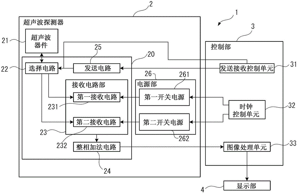
如图1所示,本实施方式的超声波装置1构成为包括超声波探测器2(超声波模块)、控制部3、和显示部4。需要注意的是,既可以采用超声波探测器2、控制部3和显示部4分别单独地构成的构成,也可以采用例如超声波探测器2、控制部3以及显示部4组装在壳体内而一体构成的构成。As shown in FIG. 1 , the
该超声波装置1从超声波探测器2的超声波器件21向生物体等目标物发送超声波,由超声波器件21接收被目标物的内部组织反射的超声波。然后,由接收电路23将超声波器件21接收到超声波时输出的接收信号处理为回波信号,并通过整相加法电路(phasingaddition circuit)24对该回波信号进行相加处理。于是,控制部3基于由整相加法电路相加处理后的相加信号,生成目标物的内部断层图像(B模式图像),并在显示部4显示。The
下面,对超声波装置1的各构成进行详细说明。Next, each configuration of the
(超声波探测器2的构成)(Configuration of Ultrasonic Probe 2)
如图1所示,超声波探测器2具备超声波器件21、发送接收部20(配线基板)、和电源部26。此外,在发送接收部20中设置有选择电路22、接收电路23、整相加法电路24、和发送电路25。As shown in FIG. 1 , the
(超声波器件的构成)(Constitution of Ultrasonic Device)
图2是示出本实施方式的超声波器件21的概略构成的截面图。FIG. 2 is a cross-sectional view showing a schematic configuration of the
图3是示出超声波器件21中的元件基板41的概略构成的俯视图。FIG. 3 is a plan view showing a schematic configuration of the
如图2所示,超声波器件21包括元件基板41、密封板42、声匹配层43、和声透镜44。As shown in FIG. 2 , the
如图2所示,元件基板41具备基板主体部411、设置于基板主体部411的密封板42侧的振动膜412、和层叠于振动膜412的压电元件413。元件基板41在如图3所示的从基板厚度方向看的俯视观察中,元件基板41的中央区域具备阵列区域Ar1,在该阵列区域Ar1中,多个超声波元件45呈矩阵状配置。As shown in FIG. 2 , the
基板主体部411例如是Si等的半导体基板。在基板主体部411的阵列区域Ar1内设置有与各个超声波元件45对应的开口部411A。此外,各开口部411A被设置于基板主体部411的背面41A侧(密封板42侧)的振动膜412堵住。The substrate
振动膜412例如由SiO2、SiO2和ZrO2的层叠体等构成,设置为覆盖基板主体部411的整个背面41A侧。该振动膜412的厚度尺寸为相对于基板主体部411足够小的厚度尺寸。The vibrating
并且,如图2所示,在堵住各开口部411A的振动膜412上,分别设置有作为下部电极414、压电膜415、以及上部电极416的层叠体的压电元件413。这里,由堵住开口部411A的振动膜412以及压电元件413构成一个超声波元件45。Further, as shown in FIG. 2 ,
在这样的超声波元件45中,通过在下部电极414与上部电极416之间施加规定周期的矩形波电压,可以使开口部411A的开口区域内的振动膜412振动,从而发出超声波。此外,如果由于从目标物反射的超声波而导致振动膜412振动,则在压电膜415的上下产生电位差。因此,通过检测下部电极414与上部电极416之间产生的所述电位差,可以检测出接收到的超声波。In such an
此外,在本实施方式中,如图3所示,在元件基板41的规定的阵列区域Ar1内,沿X方向(切片(スライス)方向)以及与X方向交差(本实施方式中为正交)的Y方向(扫描方向、本发明中的一个方向)配置多个上述那样的超声波元件45,从而构成超声波阵列46。Further, in this embodiment, as shown in FIG. 3 , in the predetermined array region Ar1 of the
这里,下部电极414沿X方向直线状形成。即、下部电极414跨沿X方向排列的多个超声波元件45而设置,并在阵列区域Ar1外的端子区域Ar2中构成第一电极垫414P。Here, the
另一方面,在阵列区域Ar1内的各压电元件413彼此间,上部电极416相互连接,其一部分引出至端子区域Ar2,构成第二电极垫416P。On the other hand, among the
在上述这样的构成中,由下部电极414所连接的沿X方向排列的超声波元件45构成一个超声波元件组45A,构成该超声波元件组45A沿Y方向排列多个的一维阵列结构的超声波阵列46。In the above configuration, one
密封板42接合于元件基板41的背面41A侧,用于增强元件基板41的强度。在与该元件基板41的阵列区域Ar1相对的区域中形成有与元件基板41的开口部411A对应的多个凹槽421。由此,在振动膜412中的由于超声波元件45而振动的区域内(开口部411A内),与元件基板41之间设置有规定尺寸的间隙,从而不会阻碍振动膜412的振动。此外,可以抑制来自于一个超声波元件45的背面波射入其它相邻的超声波元件45的不良情况(串扰)。The sealing
此外,如果振动膜412振动,则除了开口部411A侧(工作面41B侧)之外,密封板42侧(背面41A侧)也发出超声波作为背面波。该背面波被密封板42反射,再次通过间隙向振动膜412侧发射。此时,如果反射背面波和从振动膜412向工作面41B侧发出的超声波的相位错开,则超声波衰减。因此,在本实施方式中,设定各凹槽421的槽深度,以使间隙中的声程(声学距离(音響的な距離))为超声波的波长λ的四分之一(λ/4)的奇数倍。换言之,考虑从超声波元件45发出的超声波的波长λ来设定元件基板41、密封板42的各部的厚度尺寸。Further, when the vibrating
如图2所示,声匹配层43设置于元件基板41的工作面41B侧。具体而言,声匹配层43填充于元件基板41的开口部411A内,并且,从基板主体部411的工作面41B侧以规定的厚度尺寸而形成。As shown in FIG. 2 , the
声透镜44设置于声匹配层43上,其表面为超声波发送接收端面。The
这些声匹配层43、声透镜44将从超声波元件45发送的超声波高效地向目标物传播,此外,将在目标物内反射的超声波高效地向超声波元件45传播。为此,声匹配层43以及声透镜44被设定为元件基板41的超声波元件45的声阻抗与目标物的声阻抗的中间的声阻抗。在目标物是生物体的情况下,作为上述这样的声阻抗的原材料,例如可以列举出硅酮等。The
上述这样的超声波器件21配置于发送接收部20上,各电极垫414P、416P与设置于发送接收部20上的连接端子连接。这里,第二电极垫416P与基准电位电路连接,被设定为基准电位(例如0电位)。另一方面,第一电极垫414P所连接的连接端子与选择电路22连接。The
(发送接收部20以及电源部26的构成)(Configuration of the transmission/
下面,对设置于发送接收部20的选择电路22、接收电路23、向接收电路23等提供电力的电源部26、整相加法电路24以及发送电路25进行说明。此外,虽然省略了图示,但是,在发送接收部20中设置有开关电路等,该开关电路等具有在超声波的发送处理时进行钳位(クランプ),以使规定电压以上的信号不会进入接收电路23的功能。Next, the
选择电路22是切换连接于第一电极垫414P的各连接端子(驱动连接端子)与接收电路23及发送电路25的连接状态的开关电路。即、在进行从超声波器件21发送超声波的发送处理时,选择电路22连接各驱动连接端子和发送电路25。此外,在进行接收来自于目标物的超声波的接收处理时,选择电路22连接各驱动连接端子和接收电路23。The
接收电路23构成为包括第一接收电路231和第二接收电路232。The receiving
图4是示出接收电路23的各接收电路231、232与超声波器件21的各超声波元件组45A的连接关系的图。需要注意的是,在图4中,省略了选择电路22的图示。FIG. 4 is a diagram showing a connection relationship between each of the
如图1以及图4所示,接收电路23具备第一接收电路231和第二接收电路232。第一接收电路231与超声波器件21的沿扫描方向排列的超声波元件组45A中的奇数编号的超声波元件组45A电连接。此外,第二接收电路232与超声波器件21的沿扫描方向排列的超声波元件组45A中的偶数编号的超声波元件组45A电连接。As shown in FIGS. 1 and 4 , the receiving
第一接收电路231具备对应奇数编号的各超声波元件组45A而分别设置的多个接收部。这些接收部是基于从各超声波元件组45A输入的接收信号(模拟信号)生成回波信号(数字信号)的电路,具体而言,具备放大器23A、高通滤波器(HPF 23B)、和A/D转换器(A/D23C)。The
第二接收电路232也具有相同的构成,具备对应偶数编号的各超声波元件组45A而分别设置的多个接收部,这些接收部具备放大器23A、高通滤波器(HPF 23B)、和A/D转换器(A/D 23C)。The
通过第一接收电路231的各接收部处理后的各接收信号分别作为第一回波信号向整相加法电路24输出。在本实施方式中,该第一回波信号相当于本发明中的第一处理信号。Each received signal processed by each receiving unit of the
此外,通过第二接收电路232的各接收部处理后的各接收信号分别作为第二回波信号向整相加法电路24输出。在本实施方式中,该第二回波信号相当于本发明中的第二处理信号。In addition, each received signal processed by each receiving unit of the
此外,这些第一接收电路231以及第二接收电路232被从电源部26提供的电力所驱动。Further, these
具体而言,电源部26具备第一开关电源261以及第二开关电源262。这些第一开关电源261以及第二开关电源262分别具有相同的构成。即、这些第一开关电源261、第二开关电源262通过半导体开关元件的开通、关断控制,以该开通、关断的切换周期(开关周期)来稳定提供驱动电压。Specifically, the
但是,这样的开关电源261、262产生1阶至N阶周期的开关噪声。这里,频带外的低频噪声被HPF23B滤掉,但是,频带内的N阶的开关噪声并未被HPF23B滤掉而是残留了下来。因此,来自于由电源部26提供电力的各接收电路231、232的回波信号(第一回波信号、第二回波信号)上也叠置有该N阶的开关噪声。这样的开关噪声虽然越高阶(N阶)越小,但是,通过整相相加(phasing addition),开关噪声叠加(superimposition)而变大,产生伪影。However, such
这里,在本实施方式中,基于后述的控制部3的控制,第一开关电源261的驱动定时(第一驱动定时)与第二开关电源262的驱动定时(第二驱动定时)错开所述开关噪声的半周期。即、在根据第一驱动定时驱动了第一开关电源261之后,在延迟了开关噪声的半周期的第二驱动定时驱动第二开关电源262。Here, in the present embodiment, the driving timing (first driving timing) of the first
为此,叠置于从第二接收电路232输出的第二回波信号上的开关噪声相对于叠置于从第一接收电路231输出的第一回波信号上的开关噪声,也是延迟了开关噪声的半周期而叠置的。For this reason, the switching noise superimposed on the second echo signal output from the
整相加法电路24对从第一接收电路231输入的第一回波信号和从第二接收电路232输入的第二回波信号进行整相相加处理,并将相加信号向控制部3输出。此时,整相加法电路24根据深度方向上的测定位置(超声波反射位置)与各超声波元件组45A之间的距离、超声波的发送定时等,对回波信号的相位进行适当调整并相加来对各信号进行相加处理。即、在本实施方式中,整相加法电路24相当于本发明的信号加法部。The phasing and adding
这里,在超声波器件21附近的反射位置反射超声波时,从该反射位置连接至各超声波元件组45A的线段所成的角度大。即、在超声波器件21附近,各超声波元件组45A中的超声波的接收定时产生比较大的延迟。为此,在对回波信号(第一回波信号、第二回波信号)进行整相相加的情况下,在整相处理时,各回波信号的相移量也较大。这种情况下,即使如上所述在各回波信号上叠置有开关噪声,该开关噪声也会被分散,成为可以忽视开关噪声的影响的程度。Here, when an ultrasonic wave is reflected at a reflection position in the vicinity of the
另一方面,在距超声波器件21的距离远(规定值以上)的反射位置反射超声波时,从该反射位置连接至各超声波元件组45A的线段所成的角度小。这种情况下,各超声波元件组45A中的超声波的接收定时几乎为同时(几乎不会产生延迟)。为此,在对回波信号(第一回波信号、第二回波信号)进行整相相加的情况下,在整相处理时,各回波信号的相移量小,不会产生上述的开关噪声分散。On the other hand, when an ultrasonic wave is reflected at a reflection position far from the ultrasonic device 21 (a predetermined value or more), the angle formed by the line segment connecting each
图5是示出现有的接收电路以及整相加法电路的图。此外,图6是基于通过图5处理后的相加信号而生成的内部断层图像的一个例子。FIG. 5 is a diagram showing a conventional receiving circuit and a phasing and adding circuit. In addition, FIG. 6 is an example of an internal tomographic image generated based on the addition signal processed in FIG. 5 .
这里,在图5所示那样的现有的接收电路中,开关噪声叠置于与从接收电路部输出的各回波信号大致相同的位置上。在这种情况下,如果通过整相加法电路将各回波信号相加,则开关噪声相加,如图6所示,在内部断层图像上产生伪影A。Here, in the conventional receiving circuit as shown in FIG. 5 , the switching noise is superimposed on substantially the same position as each echo signal output from the receiving circuit unit. In this case, if the echo signals are added by the phasing and adding circuit, the switching noise is added, and as shown in FIG. 6 , an artifact A is generated on the internal tomographic image.
图7的(A)是示出本实施方式中的第一开关电源261的开关周期的图、(B)是示出第一回波信号的信号波形的图、(C)是示出第二开关电源262的开关周期的图、(D)是示出第二回波信号的信号波形的图、(E)是示出相加信号的信号波形的图。图7的(D)中的虚线表示第一回波信号。(A) of FIG. 7 is a diagram showing a switching cycle of the first
本实施方式中,如图7的(A)、(C)所示,在以开关周期T驱动第一开关电源261之后(第一驱动定时),在延迟了开关噪声的半周期的第二驱动定时,以和第一开关电源261相同的开关周期T驱动第二开关电源262。需要注意的是,在图7所示的例子中,是叠置开关3阶(3次)周期的开关噪声的例子。In the present embodiment, as shown in (A) and (C) of FIG. 7 , after the first
为此,如图7的(B)、(D)所示,相对于叠置于第一回波信号的开关噪声,叠置于第二回波信号的开关噪声也延迟半周期。For this reason, as shown in (B) and (D) of FIG. 7 , the switching noise superimposed on the second echo signal is also delayed by a half cycle with respect to the switching noise superimposed on the first echo signal.
为此,在整相加法电路24中,如果对第一回波信号和第二回波信号进行相加处理,则如图7的(E)所示,各开关噪声之间彼此抵消而衰减。Therefore, in the phasing and adding
发送电路25基于控制部3的控制,向超声波器件21的各超声波元件组45A输出驱动信号(脉冲信号)。由此,从各超声波元件组45A输出超声波。此时,通过依次使向各超声波元件组45A输出的驱动信号延迟,可以控制从超声波器件21发送的超声波的输出方向。The
(控制部3的构成)(Configuration of the control unit 3)
控制部3构成为包括存储器等存储部、CPU(Central Processing Unit:中央处理单元)等运算电路,通过读入并执行存储于存储器中的各种程序,从而控制部3如图1所示,作为发送接收控制单元31、时钟控制单元32以及图像处理单元33而发挥功能。The
例如,如果从操作单元(省略图示)输入意为实施超声波测定的操作信号,则发送接收控制单元31向选择电路22以及发送电路25输出驱动指令信号。For example, when an operation signal for performing ultrasonic measurement is input from an operation unit (not shown), the transmission/
时钟控制单元32向第一开关电源261以及第二开关电源262输出时钟信号。即、时钟控制单元32向第一开关电源261输出意为在第一驱动定时t1(参照图7)开始开关周期T的驱动的时钟信号。此外,时钟控制单元32向第二开关电源262输出意为在比第一驱动定时t1延迟了开关噪声的半周期tn的第二驱动定时t2开始开关周期T的驱动的时钟信号。The
图像处理单元33是本发明的图像处理部,其基于从整相加法电路24输入的各相加信号,生成内部断层图像。The
(超声波装置1的驱动方法)(Method of Driving Ultrasonic Device 1 )
下面,对使用了上述那样的超声波装置1的超声波测定方法(驱动方法)进行说明。Next, an ultrasonic measurement method (driving method) using the above-described
图8是示出本实施方式的超声波装置1的驱动方法的流程图。FIG. 8 is a flowchart showing a method of driving the
例如,如果从省略图示的操作单元向超声波装置1输入了意为开始超声波测定的操作信号,则控制部3的发送接收控制单元31生成驱动指令信号并向超声波探测器2输出(步骤S1)。For example, when an operation signal for starting ultrasonic measurement is input to the
超声波探测器2的选择电路22基于驱动指令信号,首先,连接各驱动连接端子(连接于各第一电极垫414P的连接端子)和发送电路25(步骤S2)。Based on the drive command signal, the
然后,发送电路25基于驱动指令信号对各超声波元件组45A施加驱动信号,使其发送超声波(步骤S3)。此时,通过延迟驱动信号来施加于超声波元件组45A,从而各超声波元件组45A的超声波的输出定时延迟,可以使超声波的输出方向沿扫描方向变化。即、可以使超声波对以超声波阵列46为中心的扇形的测定范围进行扫描。Then, the
此外,如果在步骤S1中从发送接收控制单元31向超声波探测器2输出驱动指令信号,则时钟控制单元32向第一开关电源261以及第二开关电源262输出时钟信号(步骤S4)。也就是说,如上所述,时钟控制单元32在第一驱动定时t1向第一开关电源261输出时钟信号,在比第一驱动定时t1延迟了开关噪声的半周期tn的第二驱动定时t2向第二开关电源262输出时钟信号。Further, when a drive command signal is output from the transmission/
需要注意的是,步骤S4的处理可以与步骤S1同时进行,如果是在后述的超声波接收处理(步骤S5)之前实施的话,可以是任何定时。It should be noted that the process of step S4 may be performed simultaneously with step S1, and any timing may be used if it is performed before the ultrasonic wave reception process (step S5) described later.
在步骤S3的超声波的发送处理之后,选择电路22基于来自于控制部3的驱动指令信号,连接各驱动连接端子和接收电路23。由此,如图4所示,沿扫描方向排列的奇数编号的超声波元件组45A与第一接收电路231连接,偶数编号的超声波元件组45A与第二接收电路232连接。即、奇数编号的超声波元件组45A构成本发明的第一超声波接收部,偶数编号的超声波元件组45A构成本发明的第二超声波接收部。After the ultrasonic wave transmission process in step S3 , the
然后,如果通过步骤S3发送的超声波被目标物的内部组织所反射,则该反射超声波被各超声波元件组45A接收,接收信号输入至接收电路23(第一接收电路231、第二接收电路232)(步骤S5)。Then, when the ultrasonic wave transmitted in step S3 is reflected by the internal tissue of the target, the reflected ultrasonic wave is received by each
然后,经第一接收电路231处理后的第一回波信号以及经第二接收电路232处理后的第二回波信号被输入至整相加法电路24,整相加法电路24对这些回波信号进行整相相加处理(步骤S6)。Then, the first echo signal processed by the
此时,通过步骤S4,从第一驱动定时t1起向第一接收电路231提供开关周期T的电力,从第二驱动定时t2起向第二接收电路232提供开关周期T的电力。因此,如图7的(B)、(D)所示,叠置于从第一接收电路231输出的第一回波信号上的开关噪声与叠置于从第二接收电路232输出的第二回波信号上的开关噪声在错开了该开关噪声的半周期的时机出现。At this time, in step S4, the power for the switching period T is supplied to the
因此,如图7的(E)所示,如果将这些回波信号相加,则输出开关噪声衰减后的相加信号。Therefore, as shown in (E) of FIG. 7 , when these echo signals are added, an added signal in which the switching noise is attenuated is output.
然后,如果由整相加法电路24实施整相相加处理,并将该相加信号输入至控制部3,则图像处理单元33基于该相加信号生成目标物的内部断层图像(步骤S7),并显示于显示部4(步骤S8)。Then, when the phasing and adding process is performed by the phasing and adding
需要注意的是,关于基于相加信号的图像生成处理,可以采用现有的方法,故在此省略说明。It should be noted that, regarding the image generation process based on the added signal, an existing method can be used, so the description is omitted here.
(本实施方式的作用效果)(Operation and effect of this embodiment)
在本实施方式的超声波装置1中,超声波探测器2(超声波模块)具备接收电路23,该接收电路23接收来自于接收超声波的超声波器件21的接收信号,生成回波信号。该接收电路23具备第一接收电路231以及第二接收电路232,第一接收电路231从第一驱动定时t1起按开关周期T被第一开关电源261驱动,输出第一回波信号。此外,第二接收电路232从比第一驱动定时延迟了开关噪声的半周期tn的第二驱动定时起按开关周期T被第二开关电源262驱动,输出第二回波信号。In the
为此,叠置于第一回波信号的开关噪声与叠置于第二回波信号的开关噪声错开该开关噪声的半周期tn。因此,如果通过整相加法电路24对这些第一回波信号以及第二回波信号进行相加处理,则开关噪声之间彼此抵消而衰减。由此,可以抑制相加信号中的开关噪声,能够实施高精度的超声波测定。For this reason, the switching noise superimposed on the first echo signal and the switching noise superimposed on the second echo signal are staggered by the half period tn of the switching noise. Therefore, when the first echo signal and the second echo signal are added by the phasing and adding
此外,超声波装置1的图像处理单元33基于这样的相加信号,生成图像。在这种情况下,所生成的图像中不会产生源于开关噪声的伪影,能够生成基于高精度的测定结果的目标物的内部断层图像。Further, the
此外,在本实施方式中,通过控制第一开关电源261以及第二开关电源262的驱动定时,可以容易地实现开关噪声的降低。因此,可以简化用于去除各回波信号中包含的噪声的滤波器等的构成,此外,在图像处理单元33中,也不需要进行用于去除开关噪声的滤波处理,还可以实现处理的简化。In addition, in the present embodiment, by controlling the driving timings of the first
在本实施方式的超声波探测器2中,超声波器件21具有沿扫描方向排列的多个超声波元件组45A,这些超声波元件组45A中的奇数编号的超声波元件组45A连接于第一接收电路231,偶数编号的超声波元件组45A连接于第二接收电路232。In the
一般而言,在离得远的超声波元件组45A之间,当接收在规定的反射位置反射的超声波时会产生延迟。这种情况下,在整相加法电路24的整相相加处理中,当整合该接收超声波的相位时,有时会相移量多。这种情况下,由于开关噪声也会相同程度地移动,因此,有时开关噪声的位置会相互错开而无法充分地衰减。针对于此,在本实施方式中,对相邻的超声波元件组45A彼此的回波信号进行相加处理,从而整相加法时的相移量小,可以有效地降低开关噪声。Generally, between the
在本实施方式中,控制部3具备指示各开关电源261、262的驱动定时t1、t2以及开关周期T的时钟控制单元32。In the present embodiment, the
通常,开关电源内置有时钟,其基于从该时钟输出的时钟周期而被驱动。但是,在这种情况下,需要将第一开关电源261的时钟周期输入第二开关电源262,并且,在第二开关电源262中,需要与和所输入的时钟周期错开了开关噪声的半周期tn的定时同步地进行驱动,从而电路构成和控制变得复杂。针对于此,在本实施方式中,通过控制部3的时钟控制单元32来控制第一开关电源261以及第二开关电源262的驱动定时,因此,只要对各第一开关电源261、第二开关电源262指示驱动定时即可,能够实现构成以及处理的简化。Generally, a switching power supply has a built-in clock and is driven based on a clock cycle output from the clock. However, in this case, it is necessary to input the clock cycle of the first
(第二实施方式)(Second Embodiment)
下面,对本发明所涉及的第二实施方式进行说明。Next, a second embodiment according to the present invention will be described.
在上述第一实施方式中,沿扫描方向排列的多个超声波元件组45A中,奇数编号的超声波元件组45A连接于第一接收电路231,偶数编号的超声波元件组45A连接于第二接收电路232。针对于此,在本实施方式中,不同点是,连接于第一接收电路231以及第二接收电路232的超声波元件组45A相对于扫描方向的中心分为一侧和另一侧。需要注意的是,在下面的说明中,对于已经说明了的构成和处理,标注相同的符号,省略或简化其说明。In the above-described first embodiment, among the plurality of
图9是示出接收电路23的第一接收电路231及第二接收电路232与超声波器件的各超声波元件组的连接状态的图。9 is a diagram showing a connection state of the
如图9所示,在本实施方式中,配置于超声波阵列46的扫描方向(Y方向)上的中心位置Y0的一侧(图9中的Y1侧)的各超声波元件组45A连接于第一接收电路231。此外,配置于中心位置Y0的另一侧(图9中的Y2侧)的各超声波元件组45A连接于第二接收电路232。即、配置于Y1侧的各超声波元件组45A构成本发明的第一超声波接收部,配置于Y2侧的各超声波元件组45A构成本发明的第二超声波接收部。As shown in FIG. 9 , in the present embodiment, each
需要说明的是,关于其它的构成,与上述第一实施方式相同。In addition, about other structures, it is the same as that of the said 1st Embodiment.
本实施方式中,在发送接收部20中实现各驱动连接端子与接收电路23的配线构成的简化。In this embodiment, the transmission/
(第三实施方式)(third embodiment)
下面,对本发明所涉及的第三实施方式进行说明。Next, a third embodiment according to the present invention will be described.
在上述第一实施方式中,接收电路23由第一接收电路231以及第二接收电路232构成,并与它们对应地设置第一开关电源261以及第二开关电源262,通过错开第一开关电源261和第二开关电源262的驱动定时(开关周期),从而抑制了开关噪声。针对于此,在第三实施方式中,则是由单一的接收电路部以及单一的开关电源构成,通过使信号取得定时延迟来降低开关噪声,这一点和上述第一实施方式不同。In the above-described first embodiment, the receiving
图10是示出第三实施方式的超声波装置1A的概略构成的框图。FIG. 10 is a block diagram showing a schematic configuration of an ultrasonic apparatus 1A according to the third embodiment.
如图10所示,本实施方式的超声波装置1A具备超声波探测器2A、控制部3A、和显示部4。As shown in FIG. 10 , the ultrasonic apparatus 1A of the present embodiment includes an
超声波探测器2A构成为包括和第一实施方式相同构成的超声波器件21、发送接收部20、和开关电源263。The
在发送接收部20中配置有选择电路22、接收电路233、整相加法电路24、和发送电路25。选择电路22、整相加法电路24、发送电路25具有和第一实施方式相同的构成。A
此外,接收电路233具有和第一接收电路231以及第二接收电路232相同的构成。该接收电路233在超声波的接收处理中通过选择电路22而与各超声波元件组45A的各第一电极垫414P所连接的各驱动连接端子电连接。并且,在接收电路233中具备多个可以分别处理来自于各超声波元件组45A的接收信号的接收部(放大器23A、HPF 23B、和A/D 23C)。In addition, the receiving
该接收电路233相当于本发明的接收电路部,被开关电源263提供的电力所驱动。开关电源263是和第一开关电源261、第二开关电源262相同的开关电源,以开关周期T来进行驱动,向接收电路233等提供电力。在本实施方式中,也是通过从控制部3A输入时钟信号,从而将该时钟信号的时钟周期作为开关周期来驱动开关电源263。The receiving
需要注意的是,在本实施方式中,也可以是开关电源263中内置有时钟的构成。在这种情况下,从开关电源263向控制部3A输入包含时钟周期的时钟信号。It should be noted that, in this embodiment, a clock may be built in the switching
控制部3A构成为包括存储器34、CPU(Central Processing Unit:中央处理单元)等运算电路,其通过读入并执行存储于存储器34中的各种程序,从而如图10所示,作为发送接收控制单元31A、时钟控制单元32以及图像处理单元33A而发挥功能。The
发送接收控制单元31A构成本发明中的超声波控制部,和第一实施方式同样,例如如果从操作单元(省略图示)输入了意为实施超声波测定的操作信号,则对选择电路22以及发送电路25输出驱动指令信号。此外,发送接收控制单元31A使超声波的发送处理和接收处理同步实施,取得1帧的图像对应的回波信号。The transmission/
这里,本实施方式的发送接收控制单元31A边错开定时,边多次实施取得所述1帧的图像对应的回波信号的超声波的发送接收处理。Here, the transmission/
即、发送接收控制单元31A交替实施:第一帧信号取得处理,与开关电源263的开关周期同步地获取对应各扫描方向的回波信号;以及第二帧信号取得处理,在相对于开关周期延迟了开关噪声的半周期tn的定时,获取对应各扫描方向的回波信号。That is, the transmission/
具体而言,发送接收控制单元31A作为定时输出单元311、发送指令单元312、和接收指令单元313而发挥功能。Specifically, the transmission/
定时输出单元311与开关电源263的开关周期同步地输出第一帧定时信号。第一帧定时信号是指示第一帧信号取得处理开始的定时信号。The
此外,定时输出单元311在从输出第一帧定时信号开始经过了规定的期间后,在相对于开关电源263的开关周期延迟了开关噪声的半周期tn的定时,输出第二帧定时信号。Furthermore,
进而,定时输出单元311在从输出第二帧定时信号开始经过了规定的期间后,与开关电源263的开关周期同步地输出第一帧定时信号。这样,定时输出单元311交替地输出第一帧定时信号和第二帧定时信号。Furthermore, the
需要说明的是,所述规定的期间是第一帧信号取得处理以及第二帧信号取得处理所涉及的时间,其根据扫描超声波的目标区域而设定。即、在使超声波扫描目标区域时,实施依次使各超声波元件组45A延迟驱动、将超声波向规定的发送方向发送的发送处理,并实施接收被目标物反射的超声波的接收处理。在上述的发送接收处理中,通过改变发送时的超声波元件组45A的驱动定时的延迟时间,从而改变超声波的发送方向,实施针对目标区域内的整个范围的反射超声波的接收处理。因此,第一帧信号取得处理以及第二帧信号取得处理所涉及的期间是到上述处理结束为止的期间。It should be noted that the predetermined period is the time involved in the first frame signal acquisition process and the second frame signal acquisition process, and is set according to the target area for scanning ultrasound. That is, when the ultrasonic wave scans the target area, the transmission processing of sequentially delaying the driving of each
发送指令单元312向超声波探测器2A输出意为发送超声波的发送指令。该发送指令中包含超声波的输出方向、即对各超声波元件组45A施加驱动信号时的延迟信息。超声波探测器2A的选择电路22在被输入了发送指令时,连接各驱动连接端子和发送电路25,从发送电路25向各超声波元件组45A输出驱动信号。The
接收指令单元313向超声波探测器2A输出意为接收超声波的接收指令。超声波探测器2A的选择电路22在被输入了接收指令时,连接各驱动连接端子和接收电路233。由此,从接收电路233向整相加法电路24输出接收信号,并从整相加法电路向控制部3输出相加信号。The
需要注意的是,关于发送接收控制单元31A的具体动作将在后面进行描述。It should be noted that the specific actions of the transmission and
图像处理单元33A将基于通过第一帧信号取得处理所取得的第一回波信号的第一相加信号和基于通过第二帧信号取得处理所取得的第二回波信号的第二相加信号相加,生成相加处理信号,并基于该相加处理信号,形成图像(内部断层图像)。The image processing unit 33A combines the first added signal based on the first echo signal acquired by the first frame signal acquisition process and the second added signal based on the second echo signal acquired by the second frame signal acquisition process The addition process generates an addition process signal, and based on the addition process signal, an image (internal tomographic image) is formed.
这里,在本实施方式中,通过第一帧信号取得处理所取得的各第一回波信号被整相加法电路24进行整相相加处理,并作为第一相加信号输出至控制部3A。第一相加信号适当地存储于控制部3A的存储器34中。Here, in the present embodiment, each first echo signal acquired by the first frame signal acquisition process is subjected to phasing and addition processing by the phasing and adding
第一相加信号是对各超声波元件组45A接收到在超声波反射位置反射的超声波时所输出的接收信号进行整相相加而得的信号。在对规定的目标区域沿超声波的发送方向进行扫描时,针对目标区域内的各超声波反射位置得到多个第一相加信号。The first addition signal is a signal obtained by phasing and adding the received signals output when each
需要注意的是,在该第一相加信号中,叠置于各第一回波信号上的开关噪声被叠加放大。即、第一相加信号为包括开关噪声的信号。在本实施方式中,第一相加信号相当于本发明中的第一处理信号。It should be noted that, in the first added signal, the switching noise superimposed on each of the first echo signals is superimposed and amplified. That is, the first added signal is a signal including switching noise. In this embodiment, the first added signal corresponds to the first processed signal in the present invention.
此外,通过第二帧信号取得处理所取得的第二回波信号也和第一回波信号同样地被整相加法电路24进行整相相加处理,并作为第二相加信号输出至控制部3A。在该第二相加信号中,第二回波信号的开关噪声被叠加放大。该开关噪声在相对于第一相加信号中的开关噪声延迟了该开关噪声的半周期tn的位置上出现。本实施方式中,第二相加信号相当于本发明中的第二处理信号。第二相加信号适当地存储于控制部3A的存储器34中。In addition, the second echo signal obtained by the second frame signal acquisition process is also subjected to the phasing and adding process by the phasing and adding
于是,图像处理单元33A读出存储于存储器34中的第一相加信号以及第二相加信号,并将这些第一相加信号以及第二相加信号相加,从而生成对应于一帧的内部断层图像的相加处理信号。此外,图像处理单元33A基于算出的相加处理信号,生成内部断层图像。此时,第一相加信号中包含的开关噪声与第二相加信号中包含的开关噪声由于相位错开半周期而彼此抵消、衰减。Then, the image processing unit 33A reads out the first added signal and the second added signal stored in the
即、在本实施方式中,图像处理单元33A作为本发明中的图像处理部以及信号加法部发挥功能。此外,通过本发明的超声波探测器2A以及控制部3A构成本发明的超声波模块。That is, in the present embodiment, the image processing unit 33A functions as an image processing unit and a signal addition unit in the present invention. In addition, the ultrasonic module of the present invention is constituted by the
如上所述,在本实施方式中,通过将对应两帧的图像的相加信号(第一相加信号以及第二相加信号)相加,从而生成对应一帧的图像的相加处理信号。As described above, in the present embodiment, the addition processing signal corresponding to the image of one frame is generated by adding the addition signals (the first addition signal and the second addition signal) corresponding to the images of two frames.
(超声波装置1A的驱动方法)(Method of Driving Ultrasonic Device 1A)
下面,对采用了上述那样的超声波装置1A的超声波测定方法(驱动方法)进行说明。Next, an ultrasonic measurement method (driving method) using the above-described ultrasonic apparatus 1A will be described.
图11是示出本实施方式的超声波装置1A的驱动方法的流程图。FIG. 11 is a flowchart showing a driving method of the ultrasonic device 1A according to the present embodiment.
图12是开关电源263的开关周期、帧定时信号、超声波的发送定时信号、以及超声波的接收定时信号的时序图。12 is a timing chart of the switching cycle of the switching
在超声波装置1A的超声波测定处理中,例如从省略图示的操作单元输入了意为开始超声波测定的操作信号时,控制部3A的发送接收控制单元31A通过时钟控制单元32向开关电源263输出时钟信号(步骤S21)。由此,如图12的(A)所示,以开关周期T来驱动开关电源263。In the ultrasonic measurement process of the ultrasonic apparatus 1A, for example, when an operation signal for starting ultrasonic measurement is input from an operation unit (not shown), the transmission/
接着,发送接收控制单元31A的定时输出单元311输出帧定时信号(步骤S22)。具体而言,如图12的(B)所示,定时输出单元311与开关周期同步地输出第一帧定时信号。此外,定时输出单元311在从第一帧定时信号的输出定时开始经过了第一帧信号取得处理所涉及的规定期间后,在与开关周期延迟了开关噪声的半周期tn的定时,输出第二帧定时信号。之后,定时输出单元311继续进行第一帧定时信号和第二帧定时信号的输出。Next, the
此外,发送接收控制单元31A判断是否输出了第一帧定时信号(步骤S23)。Further, the transmission and
在步骤S23中判断为否时,返回步骤S23,继续进行第一帧定时信号的检测。When it is determined as NO in step S23, the process returns to step S23, and the detection of the first frame timing signal is continued.
在步骤S23中判断为是时(图12中的定时t21),开始第一帧信号取得处理。When the determination is YES in step S23 (timing t21 in FIG. 12 ), the first frame signal acquisition process is started.
在该第一帧信号取得处理中,发送指令单元312与开关周期同步(与开关周期的上升沿同步)地输出发送指令信号。即、选择电路22连接各驱动连接端子和发送电路25,实施发送处理(步骤S24)。此外,如图12的(C)所示,发送指令单元312将发送定时信号与发送指令信号同时地输出。发送定时信号的输出期间是直至从超声波探测器2A向规定方向发送超声波结束为止的时间,例如从各超声波元件组45A输出1~3脉冲的超声波。In this first frame signal acquisition process, the
接着,如图12的(D)所示,接收指令单元313与发送定时信号的下降沿定时t22同步地向超声波探测器2A输出接收指令信号。即、选择电路22连接各驱动连接端子和接收电路233,实施接收处理(步骤S25)。此外,如图12的(D)所示,接收指令单元313将接收定时信号与接收指令信号同时地输出。接收定时信号的输出期间是可以通过超声波探测器2A接收来自于目标区域的反射超声波的期间。通过该步骤S25检测超声波的发送方向上的各深度的反射超声波,从接收电路233向整相加法电路24输出第一回波信号。由此,从整相加法电路24向控制部3A输出第一相加信号,该第一相加信号存储于存储器34。Next, as shown in (D) of FIG. 12 , the
然后,发送接收控制单元31A判断对于目标区域的超声波扫描是否结束(步骤S26)。需要注意的是,在步骤S26中,既可以判断对于针对目标区域所设定的所有方向的超声波的发送接收处理(步骤S24以及步骤S25)是否结束,也可以判断是否经过了针对第一帧信号取得处理所预先设定的时间。Then, the transmission/
在步骤S26中判断为否时,则返回步骤S24,如图12的定时t23、t24所示,继续进行和开关周期同步的超声波的发送接收处理。When the determination in step S26 is NO, the process returns to step S24, and as shown at timings t23 and t24 in FIG. 12 , the ultrasonic wave transmission and reception processing synchronized with the switching cycle is continued.
另一方面,在步骤S26中判断为是时,发送接收控制单元31A通过定时输出单元311判断是否输出了第二帧定时信号(步骤S27)。On the other hand, when the determination is YES in step S26, the transmission/
在步骤S27中判断为否时,则返回步骤S27,继续进行第二帧定时信号的输出检测。When it is judged as NO in step S27, the process returns to step S27, and the output detection of the second frame timing signal is continued.
在步骤S27中判断为是时(图12的定时t25),开始第二帧信号取得处理。When it is determined as YES in step S27 (timing t25 in FIG. 12 ), the second frame signal acquisition process is started.
在该第二帧信号取得处理中,发送指令单元312在相对于开关周期延迟了开关噪声的半周期tn的定时t25输出发送指令信号。即、实施发送处理(步骤S28)。此外,发送指令单元312和第一帧信号取得处理同样地将发送定时信号与发送指令信号同时地输出。In this second frame signal acquisition process, the
接着,如图12的(D)所示,接收指令单元313和发送定时信号的下降沿定时t26同步地向超声波探测器2A输出接收指令信号。即、实施接收处理(步骤S29)。并且,接收指令单元313和第一帧信号取得处理同样地将接收定时信号与接收指令信号同时地输出。通过该步骤S29,检测出超声波的发送方向上的各深度的反射超声波,并从接收电路233向整相加法电路24输出第二回波信号。由此,从整相加法电路24向控制部3A输出第二相加信号,该第二相加信号存储于存储器34。Next, as shown in (D) of FIG. 12 , the
然后,发送接收控制单元31A判断对于目标区域的超声波扫描是否结束(步骤S30)。需要注意的是,在步骤S30中,和步骤S26同样,既可以判断对于针对目标区域所设定的所有方向的超声波的发送接收处理(步骤S28以及步骤S29)是否结束,也可以判断是否经过了针对第二帧信号取得处理所预先设定的时间。Then, the transmission/
在步骤S30中判断为否时,则返回步骤S28,如图12的定时t27、t28所示,继续进行和开关周期同步的超声波的发送接收处理。When it is determined NO in step S30, the process returns to step S28, and as shown at timings t27 and t28 in FIG. 12, the ultrasonic wave transmission and reception processing synchronized with the switching cycle is continued.
另一方面,在步骤S30中判断为是时,图像处理单元33A分别读出存储于存储器34的第一相加信号和第二相加信号(步骤S31)。On the other hand, when YES is determined in step S30, the image processing unit 33A reads out the first added signal and the second added signal stored in the
然后,图像处理单元33A将这些第一相加信号和第二相加信号中的、超声波反射方向(发送方向)相同的信号彼此相加,生成相加处理信号(步骤S32)。这里,第一相加信号和第二相加信号均叠置有开关噪声,通过整相相加处理,成为该开关噪声叠加的信号。但是,第一相加信号中的开关噪声和第二相加信号中的开关噪声存在于错开半周期tn的位置上,因此,通过如上所述地对第一相加信号和第二相加信号进行相加处理,从而这些开关噪声彼此抵消而衰减。Then, the image processing unit 33A adds the signals having the same ultrasonic reflection direction (transmission direction) among the first and second added signals to each other to generate an addition processed signal (step S32 ). Here, both the first added signal and the second added signal are superimposed with switching noise, and through the phasing and addition processing, the switching noise superimposed signal becomes a signal. However, the switching noise in the first added signal and the switching noise in the second added signal exist at positions shifted by the half period tn. Therefore, by comparing the first added signal and the second added signal as described above The addition process is performed so that these switching noises cancel each other and are attenuated.
然后,图像处理单元33A基于在步骤S31中算出的各相加处理信号,生成目标物的内部断层图像,并在显示部4上显示(步骤S33)。Then, the image processing unit 33A generates an internal tomographic image of the object based on the respective addition processing signals calculated in step S31, and displays it on the display unit 4 (step S33).
此外,控制部3A判断是否继续进行通过超声波的内部断层图像的测定(步骤S34)。在步骤S34中判断为是时,则返回步骤S23。Further, the
(本实施方式的作用效果)(Operation and effect of this embodiment)
在本实施方式的超声波装置1A中,超声波探测器2A具备:超声波器件21;发送电路25,实施利用了超声波器件21的超声波的发送处理;以及接收电路233,对来自于超声波器件21的各超声波元件组45A的接收信号进行处理,并输出回波信号。该接收电路233被来自于开关电源263的电力所驱动,该开关电源263以规定的开关周期T而被驱动。In the ultrasonic apparatus 1A of the present embodiment, the
并且,控制部3A的发送接收控制单元31A与开关周期同步地实施超声波的发送接收处理。此时,由整相加法电路24对从接收电路233输出的第一回波信号进行整相相加处理,并作为第一相加信号存储于存储器34中。此外,控制部3A的发送接收控制单元31A在相对于开关周期延迟了开关噪声的半周期tn的定时实施超声波的发送接收处理。此时,由整相加法电路24对从接收电路233输出的第二回波信号进行整相相加处理,并作为第二相加信号向控制部3A输出。然后,图像处理单元33A对存储器34中存储的第一相加信号和第二相加信号进行相加处理,并将其作为相加处理信号输出。Then, the transmission/
在这样构成的超声波装置1A中,叠置于第一相加信号(第一回波信号)上的开关噪声和叠置于第二相加信号(第二回波信号)上的开关噪声错开开关噪声的半周期tn而出现。为此,如果将这些第一相加信号和第二相加信号相加,则彼此的开关噪声抵消,其结果是降低开关噪声。因此,和第一实施方式同样,可以获得高精度的超声波测定结果,能够生成针对目标物的高精度的内部断层图像。In the ultrasonic apparatus 1A configured in this way, the switching noise superimposed on the first added signal (first echo signal) and the switching noise superimposed on the second added signal (second echo signal) are shifted by switching. The half period tn of the noise appears. For this reason, when these first addition signals and second addition signals are added, the switching noise of each other is canceled, and as a result, the switching noise is reduced. Therefore, as in the first embodiment, a high-precision ultrasonic measurement result can be obtained, and a high-precision internal tomographic image of the target can be generated.
进而,和第一实施方式相比,可以通过单一的接收电路233以及单一的开关电源263有效地降低开关噪声,实现构成的简化。此外,不管是对于具有现有的接收电路和开关电源的超声波装置、还是对于上述,光是组装入发送接收控制单元31A、时钟控制单元32以及图像处理单元33A即可容易地实现开关噪声的降低。这样的发送接收控制单元31A、时钟控制单元32以及图像处理单元33A例如可以通过CPU等运算电路读入并执行存储于存储器34等存储单元中的程序来构成。因此,也可以通过例如将具有这些功能的应用程序软件安装于现有的超声波探测器2上而容易地实现。Furthermore, compared with the first embodiment, the switching noise can be effectively reduced by the
(变形例)(Variation)
需要说明的是,本发明并不限定于上述的各实施方式,能够实现本发明目的的范围内的变形、改良以及适当组合各实施方式等所得到的构成均包含于本发明中。It should be noted that the present invention is not limited to the above-described respective embodiments, and modifications, improvements, and configurations obtained by appropriately combining the respective embodiments within a range that can achieve the object of the present invention are included in the present invention.
例如,在上述第三实施方式中,构成为将第一相加信号作为本发明的第一处理信号、将第二相加信号作为本发明的第二处理信号、将图像处理单元33A作为本发明的信号加法部来将第一相加信号和第二相加信号相加。针对于此,例如也可以构成为,在超声波探测器2中设置存储第一回波信号以及第二回波信号的存储器,通过整相加法电路对这些第一回波信号以及第二回波信号进行整相相加处理,并向控制部3A输出。在这种情况下,第一回波信号成为本发明中的第一处理信号,第二回波信号成为本发明中的第二处理信号,整相加法电路24成为本发明中的信号加法部。即使在这样的情况下,叠置于各第一回波信号的开关噪声和叠置于第二回波信号的开关噪声也是错开该开关噪声的半周期tn。因此,通过对它们进行相加处理,可以有效地降低开关噪声。For example, in the third embodiment described above, the first added signal is used as the first processed signal of the present invention, the second added signal is used as the second processed signal of the present invention, and the image processing unit 33A is used as the present invention. to add the first added signal and the second added signal. For this purpose, for example, a memory for storing the first echo signal and the second echo signal may be provided in the
在上述第一实施方式中,通过控制部3A的时钟控制单元32对第一开关电源261以及第二开关电源262输出时钟信号,使第一开关电源261与第二开关电源262的驱动周期延迟开关噪声的半周期。相对于此,也可以如上所述,从第一开关电源261向第二开关电源262输出时钟信号,在第二开关电源262中,相对于输入的时钟信号的时钟周期延迟开关噪声的半周期来进行驱动。In the above-described first embodiment, the clock signal is output to the first
在第三实施方式中,示出了从时钟控制单元32向开关电源263输出时钟信号的例子,但是,例如也可以使用现有的内置有时钟的开关电源。在这种情况下,从开关电源向控制部3A输出时钟信号。由此,发送接收控制单元31A可以基于该输入的时钟信号的时钟周期(开关周期)来取得第一相加信号以及第二相加信号。In the third embodiment, the example in which the clock signal is output from the
在第三实施方式中,示出了实施第一帧信号取得处理和第二帧信号取得处理并对第一相加信号和第二相加信号进行相加处理的例子,但不限定于此。In the third embodiment, an example in which the first frame signal acquisition process and the second frame signal acquisition process are performed and the addition process is performed on the first added signal and the second added signal is shown, but the present invention is not limited to this.
例如,也可以实施与开关频率同步的第一帧信号取得处理、相对于开关频率延迟了开关噪声的半周期的第二帧信号取得处理、与开关频率同步的第三帧信号取得处理、以及相对于开关频率延迟了开关噪声的半周期的第四帧信号取得处理。在这种情况下,对在第一帧信号取得处理中取得的第一相加信号、在第二帧信号取得处理中取得的第二相加信号、在第三帧信号取得处理中取得的第三相加信号、以及在第四帧信号取得处理中取得的第四相加信号进行相加处理,生成相加处理信号。For example, the first frame signal acquisition process synchronized with the switching frequency, the second frame signal acquisition process delayed by a half cycle of the switching noise from the switching frequency, the third frame signal acquisition process synchronized with the switching frequency, and the relative The fourth frame signal acquisition processing is delayed by a half cycle of the switching noise from the switching frequency. In this case, the first added signal acquired in the first frame signal acquisition process, the second added signal acquired in the second frame signal acquisition process, and the first added signal acquired in the third frame signal acquisition process The three-phase addition signal and the fourth addition signal acquired in the fourth frame signal acquisition process are subjected to addition processing to generate an addition processed signal.
在上述各实施方式中,作为超声波器件21,例示了具备在振动膜412上层叠薄膜状的压电元件413来输出超声波的超声波器件21的构成,但不限定于此。作为超声波器件,例如也可以采用配置于体型(バルク型)的压电体的扫描方向来进行超声波的发送接收的构成等。此外,作为超声波器件21的构成,还可以例示任何构成,例如,也可以是在隔着间隙相对的一对电极间施加交流电压而使振动膜振动的超声波元件等。In each of the above-described embodiments, as the
此外,例示了沿扫描方向配置有超声波元件组45A的一维阵列结构,但也可以构成为各超声波元件45能够分别独立地驱动的二维阵列结构。In addition, the one-dimensional array structure in which the
此外,实施本发明时的具体结构既可以通过在能达到本发明目的的范围内适当组合上述各实施方式以及变形例来构成、也可以适当变更为其它结构等。In addition, the specific structure at the time of carrying out this invention may be comprised by combining suitably the above-mentioned each embodiment and modification in the range which can achieve the objective of this invention, and may be suitably changed to another structure, etc.
Claims (9)
Applications Claiming Priority (2)
| Application Number | Priority Date | Filing Date | Title |
|---|---|---|---|
| JP2015-177319 | 2015-09-09 | ||
| JP2015177319A JP6617488B2 (en) | 2015-09-09 | 2015-09-09 | Ultrasonic module, ultrasonic device, and control method of ultrasonic module |
Publications (2)
| Publication Number | Publication Date |
|---|---|
| CN106901774A CN106901774A (en) | 2017-06-30 |
| CN106901774B true CN106901774B (en) | 2020-11-20 |
Family
ID=58190951
Family Applications (1)
| Application Number | Title | Priority Date | Filing Date |
|---|---|---|---|
| CN201610811724.3A Active CN106901774B (en) | 2015-09-09 | 2016-09-08 | Ultrasonic module, ultrasonic device, and control method of ultrasonic module |
Country Status (3)
| Country | Link |
|---|---|
| US (1) | US10631832B2 (en) |
| JP (1) | JP6617488B2 (en) |
| CN (1) | CN106901774B (en) |
Families Citing this family (5)
| Publication number | Priority date | Publication date | Assignee | Title |
|---|---|---|---|---|
| TWI644526B (en) * | 2017-02-21 | 2018-12-11 | 佳世達科技股份有限公司 | Ultrasound system and noise eliminating method |
| JP7199904B2 (en) * | 2017-10-19 | 2023-01-06 | キヤノンメディカルシステムズ株式会社 | Ultrasound diagnostic equipment and ultrasound probe |
| JP7105172B2 (en) * | 2018-11-01 | 2022-07-22 | 富士フイルムヘルスケア株式会社 | Ultrasonic probe and ultrasonic diagnostic equipment |
| JP7803135B2 (en) * | 2022-01-20 | 2026-01-21 | セイコーエプソン株式会社 | Fluidic device and method for controlling the fluidic device |
| CN114985239B (en) * | 2022-05-30 | 2024-03-26 | 青岛海信医疗设备股份有限公司 | Ultrasonic anti-interference method and ultrasonic equipment |
Citations (3)
| Publication number | Priority date | Publication date | Assignee | Title |
|---|---|---|---|---|
| JP2012065694A (en) * | 2010-09-21 | 2012-04-05 | Toshiba Corp | Ultrasonic diagnostic apparatus |
| CN102821699A (en) * | 2011-01-27 | 2012-12-12 | 株式会社东芝 | Ultrasonic probe and ultrasound diagnostic apparatus |
| CN103431873A (en) * | 2013-03-08 | 2013-12-11 | 无锡祥生医学影像有限责任公司 | Ultrasonic fuse harmonic imaging system and method |
Family Cites Families (15)
| Publication number | Priority date | Publication date | Assignee | Title |
|---|---|---|---|---|
| JPS5481334A (en) * | 1977-12-12 | 1979-06-28 | Kawasaki Kasei Chem Ltd | Preparation of highly chlorinated copper phthalocyanine |
| JPH02164351A (en) * | 1988-12-16 | 1990-06-25 | Aloka Co Ltd | Signal receiver for ultrasonic diagnostic device |
| JP2770391B2 (en) * | 1989-03-31 | 1998-07-02 | 株式会社日立メディコ | Ultrasound imaging device |
| JPH04117953A (en) * | 1990-09-10 | 1992-04-17 | Hitachi Medical Corp | Receiving wave phasing circuit and ultrasonic image pickup device using the same |
| JPH05300889A (en) | 1992-04-27 | 1993-11-16 | T Berrine Howard | Artifact removing system, artifact removing method, and signal processor for cardiogram using them |
| JPH10201732A (en) * | 1997-01-17 | 1998-08-04 | Hitachi Medical Corp | Power supply unit and magnetic resonance imaging system using it |
| US6866631B2 (en) * | 2001-05-31 | 2005-03-15 | Zonare Medical Systems, Inc. | System for phase inversion ultrasonic imaging |
| JP4495430B2 (en) * | 2003-09-26 | 2010-07-07 | パナソニック株式会社 | Ultrasonic diagnostic equipment |
| CN102078204A (en) * | 2009-12-01 | 2011-06-01 | 深圳迈瑞生物医疗电子股份有限公司 | Ultrasonic imaging system and control method thereof and continuous wave Doppler processing device |
| WO2013137061A1 (en) * | 2012-03-15 | 2013-09-19 | 日立アロカメディカル株式会社 | Ultrasonic diagnostic device and noise reduction method |
| US9229897B2 (en) * | 2012-06-29 | 2016-01-05 | Intel Corporation | Embedded control channel for high speed serial interconnect |
| JP6089499B2 (en) * | 2012-08-28 | 2017-03-08 | セイコーエプソン株式会社 | Ultrasonic transducer device and probe, electronic device and ultrasonic diagnostic device |
| JP2014083155A (en) * | 2012-10-22 | 2014-05-12 | Toshiba Corp | Ultrasound diagnostic device |
| CN102908167B (en) * | 2012-10-25 | 2016-08-03 | 武汉超信电子工程有限公司 | The cloud imaging processing system of medical ultrasonic equipment and method thereof |
| JP6387814B2 (en) * | 2014-12-08 | 2018-09-12 | コニカミノルタ株式会社 | Ultrasound diagnostic imaging equipment |
-
2015
- 2015-09-09 JP JP2015177319A patent/JP6617488B2/en active Active
-
2016
- 2016-08-31 US US15/253,082 patent/US10631832B2/en active Active
- 2016-09-08 CN CN201610811724.3A patent/CN106901774B/en active Active
Patent Citations (3)
| Publication number | Priority date | Publication date | Assignee | Title |
|---|---|---|---|---|
| JP2012065694A (en) * | 2010-09-21 | 2012-04-05 | Toshiba Corp | Ultrasonic diagnostic apparatus |
| CN102821699A (en) * | 2011-01-27 | 2012-12-12 | 株式会社东芝 | Ultrasonic probe and ultrasound diagnostic apparatus |
| CN103431873A (en) * | 2013-03-08 | 2013-12-11 | 无锡祥生医学影像有限责任公司 | Ultrasonic fuse harmonic imaging system and method |
Also Published As
| Publication number | Publication date |
|---|---|
| JP6617488B2 (en) | 2019-12-11 |
| US20170065260A1 (en) | 2017-03-09 |
| CN106901774A (en) | 2017-06-30 |
| JP2017051403A (en) | 2017-03-16 |
| US10631832B2 (en) | 2020-04-28 |
Similar Documents
| Publication | Publication Date | Title |
|---|---|---|
| CN106901774B (en) | Ultrasonic module, ultrasonic device, and control method of ultrasonic module | |
| JP5659564B2 (en) | Ultrasonic probe and ultrasonic diagnostic apparatus | |
| CN105997137B (en) | Ultrasonic signal processing device, and ultrasonic diagnostic device | |
| CN102821699B (en) | Ultrasonic probe and ultrasound diagnostic apparatus | |
| JP5560928B2 (en) | Ultrasonic probe and ultrasonic diagnostic apparatus | |
| US10307137B2 (en) | Ultrasonic device as well as probe and electronic apparatus | |
| CN104337544B (en) | Ultrasonic measurement device, head unit, detector and image device | |
| EP2832295A1 (en) | Ultrasonic probe and ultrasonic diagnostic device comprising same | |
| US20120190986A1 (en) | Ultrasound probe and ultrasound diagnostic apparatus | |
| CN101160098B (en) | Ultrasonic diagnostic device | |
| WO2006006460A1 (en) | Ultrasonic imaging device | |
| KR20160069293A (en) | Probe, Ultrasound Imaging Apparatus, and Controlling Method of the Ultrasound Imaging Apparatus | |
| US9246077B2 (en) | Ultrasonic transducer device, head unit, probe, and ultrasonic imaging apparatus | |
| CN103415256A (en) | Ultrasonic probe and ultrasonic diagnostic device | |
| JP6601190B2 (en) | Piezoelectric module, ultrasonic module and electronic device | |
| CN104013421B (en) | Ultrasonic transducer device, head unit, detector and ultrasound imaging device | |
| JP6597063B2 (en) | Ultrasonic device, ultrasonic module, and ultrasonic measuring instrument | |
| JP5836197B2 (en) | Ultrasonic diagnostic apparatus and data processing method | |
| JP6186737B2 (en) | Ultrasonic measuring device, ultrasonic imaging device, and ultrasonic measuring method | |
| JP2004089357A (en) | Ultrasonic search unit, and ultrasonic diagnostic apparatus using the same | |
| JP7093884B1 (en) | Array type ultrasonic image device and ultrasonic image display method | |
| JP7020052B2 (en) | Ultrasound signal processing device, ultrasonic diagnostic device, ultrasonic signal processing method, and ultrasonic image display method | |
| JP7187165B2 (en) | Ultrasonic probe and ultrasonic diagnostic equipment | |
| WO2022230601A1 (en) | Ultrasonic diagnostic device and method for controlling ultrasonic diagnostic device | |
| JP2017063928A (en) | Ultrasonic measurement apparatus and ultrasonic probe |
Legal Events
| Date | Code | Title | Description |
|---|---|---|---|
| PB01 | Publication | ||
| PB01 | Publication | ||
| SE01 | Entry into force of request for substantive examination | ||
| SE01 | Entry into force of request for substantive examination | ||
| GR01 | Patent grant | ||
| GR01 | Patent grant |